fundamental study of solution …d-scholarship.pitt.edu/31262/26/minlin_jiang_2017.pdffundamental...
TRANSCRIPT
i
FUNDAMENTAL STUDY OF SOLUTION PROCESSED INORGANIC HYBRID THIN
FILM SOLAR CELLS
by
Minlin Jiang
Bachelor of Science, Jiangxi Normal University, 2000
Master of Science, Shanghai Jiaotong University, 2009
Master of Science, South Dakota State University, 2012
Submitted to the Graduate Faculty of
Swanson School of Engineering in partial fulfillment
of the requirements for the degree of
Doctor of Philosophy
University of Pittsburgh
2017
ii
UNIVERSITY OF PITTSBURGH
SWANSON SCHOOL OF ENGINEERING
This dissertation was presented
by
Minlin Jiang
It was defended on
February 17, 2017
and approved by
William E Stanchina, PhD, Professor
Department of Electrical and Computer Engineering
Hong Koo Kim, PhD, Professor
Department of Electrical and Computer Engineering
Kevin Chen, PhD, Professor
Department of Electrical and Computer Engineering
Paul Leu, PhD, Associate Professor
Department of Industrial Engineering
Dissertation Director: Guangyong Li, PhD, Associate Professor
Department of Electrical and Computer Engineering

iii
Copyright © by Minlin Jiang
2017
Copyright © by Minlin Jiang
2017
iv
Solar energy is inexhaustible. It’s effective and widespread utilization is the way to prevent the
Earth from being further polluted. Solar cell has been demonstrated to be the most promising
technology to produce electricity by absorbing sunlight, with crystal silicon (c-Si) solar cell
leading the market. However, significant amount of energy is required for manufacturing of crystal
silicon solar cells because of vacuum-based fabrication process and high consumption of raw
materials.
Solution processed thin film solar cells have been considered as promising alternatives to c-
Si solar cells because of the low-cost process and low consumption of raw materials. In this work,
two types of thin film solar cells (TFSCs), namely Cu2ZnSnS4 (CZTS) and CH3NH3PbI3
(MAPbI3) have been explored with a focus on the fabrication and characterization. In the case of
FUNDAMENTAL STUDY OF SOLUTION PROCESSED INORGANIC AND
HYBRID THIN FILM SOLAR CELLS
Minlin Jiang, PhD
University of Pittsburgh, 2017
v
CZTS TFSCs, a promising efficiency of 6.2% has been obtained by modifying a water-based
process previously developed. In the case of MAPbI3 TFSCs, an efficiency of 15.39% has been
achieved from a spin-coating process. By incorporating with Cl into MAPbI3 thin film, the
efficiency was significantly increased to 18.60%. To improve the stability of MAPbI3 TFSCs, a
device structure incorporating inorganic metal oxides as charge transport layers (CTLs) has been
developed. A promising result with a highly stable and a highly efficient perovskite solar cell was
obtained.
The mechanisms behind the improvement were revealed by open-circuit voltage decay
(OCVD) measurement, admittance spectroscopy (AS), temperature-dependent open-circuit
voltage (VOC), and Kelvin probe force microscopy (KPFM). By comparing the device properties
of CZTS solar cells and MAPbI3 solar cells, it was found that the interfaces of these two types of
solar cells were crucial in improving their efficiencies. Therefore, interface engineering should be
prioritized to further improve the efficiencies of these two PV technologies.
vi
TABLE OF CONTENTS
INTRODUCTION ........................................................................................................ 1
1.1 SOLUTION-PROCESSED THIN FILM SOLAR CELLS ............................. 4
1.1.1 Cu2ZnSnS4 (CZTS) .......................................................................................... 4
1.1.2 CH3NH3PbI3 (MAPbI3) ................................................................................... 6
1.2 MOTIVATION .................................................................................................... 9
1.3 CHARACTERIZATION METHODS ............................................................. 10
1.3.1 Open-Circuit Voltage Decay (OCVD) ......................................................... 10
1.3.2 Admittance Spectroscopy (AS) ..................................................................... 13
1.3.3 Temperature-Dependent Open-Circuit Voltage ......................................... 17
1.3.4 Kelvin Probe Force Microscopy (KPFM) ................................................... 19
EFFECTS OF SELENIUM VAPOR ANNEALING ON CZTS SOLAR CELLS 21
2.1 EXPERIMENTAL PROCEDURES ................................................................ 22
2.1.1 Materials ......................................................................................................... 22
2.1.2 CZTS Precursor Solution Preparation ........................................................ 23
2.1.3 CZTS Precursor Thin Film Preparation ..................................................... 23
2.1.4 CZTS Thin Film Preparation ....................................................................... 24
2.1.5 Device Fabrication ......................................................................................... 26
vii
2.2 RESULTS AND ANALYSIS ............................................................................ 26
EFFECTS OF CHLORINE DOPING ON MAPBI3 SOLAR CELL .................... 44
3.1 EXPERIMENTAL PROCEDURES ................................................................ 45
3.1.1 Synthesis of CH3NH3I (MAI) and CH3NH3Cl (MACl) .............................. 45
3.1.2 Fabrication of MAPbI3 Solar Cells .............................................................. 46
3.1.3 Characterization ............................................................................................ 47
3.2 RESULTS AND ANALYSIS ............................................................................ 48
CHLORINE-ASSISTED RECOVERY OF PERFORMANCE LOSS IN MAPBI3
PEROVSKITE SOLAR CELL MADE FROM LOW PURITY PBI2 ................................... 66
4.1 EXPERIMENTAL PROCEDURES ................................................................ 67
4.1.1 Fabrication of MAPbI3 Solar Cells using PbI2 with different purtities.... 67
4.2 RESULTS AND ANALYSIS ............................................................................ 67
IMPROVED STABILITY OF MAPBI3 SOLAR CELLS USING ALL
INORGANIC CHARGE TRANSPORT LAYERS (CTLS) ................................................... 79
5.1 EXPERIMENTAL PROCEDURES ................................................................ 81
5.1.1 Synthesis of ZnO Nanoparticles (NPs) ......................................................... 81
5.1.2 Preparation of Li-doped NiOx (Li:NiOx) sol-gel ........................................ 81
5.1.3 Fabrication of MAPbI3 solar cell with all inorganic CTLs ........................ 82
5.2 RESULTS AND ANALYSIS ............................................................................ 83
FUTURE WORK AND CONCLUSION ................................................................. 92
viii
6.1 FUTURE WORK ............................................................................................... 92
6.1.1 Interface Engineering of CZTS Solar Cells ................................................ 92
6.1.2 Interface Engineering of MAPbI3 Solar Cells ............................................. 93
6.1.3 Effects of impurities in MAPbI3 Solar Cells ............................................... 98
6.2 CONCLUSION .................................................................................................. 98
BIBLIOGRAPHY ..................................................................................................................... 101
ix
LIST OF TABLES
Table 2.1 Chemical composition of the final CZTS thin film. ..................................................... 28
Table 2.2 Averaged I-V parameters of CZTSSe solar cells. ......................................................... 40
Table 3.1 Elemental ratios of the perovskite solar cells. .............................................................. 50
Table 3.2 I-V parameters of the best perovskite solar cells. ......................................................... 55
Table 5.1 I-V parameters the champion perovskite solar cell with different device structures. ... 86
x
LIST OF FIGURES
Figure 1.1 Market share of different PV technology. ..................................................................... 3
Figure 1.2 (a) Schematic structure of CZTS solar cell and (b) band diagram of the CdS/CZTS
heterojunction (adopted from [8]). .................................................................................................. 5
Figure 1.3 (a,c) Schematic structure and (b,d) band diagram of the perovskite solar cells with
different structures (adopted from [20] [21]). ................................................................................. 8
Figure 1.4 Illumination from a sunlight simulator and measured values of Voc at different time
(adopted from [35]). ...................................................................................................................... 12
Figure 1.5 (a) Schematic of band bending with one deep trap state, (b) charge density variation
through the depletion region due to the trap state, and (c) in response to a changing bias, dV/dt,
changes in space charge density dρ/dt can occur at both xT and W, as indicated (adopted from
[37])............................................................................................................................................... 14
Figure 1.6 (a) Raw data of Admittance Spectroscopy for a CIGS device, (b) The Admittance
Spectroscopy data after applying Eq. (2.11), showing the characteristic (peak) frequencies at each
temperature, (c) Arrhenius plot of each peak (circles) and the linear fitting (line), (d) DLCP data
(circles) in comparison of admittance spectroscopy data (-fdC/df) data (solid line) (adopted from
[37])............................................................................................................................................... 16
Figure 1.7 Temperature dependence of the open circuit voltage (VOC) and its linear extrapolation
line to 0 K for the 15.2% efficient CIGS device (dashed line) and the 10.1% efficient CZTS device
(solid line), which helps to elucidate the dominant recombination process in the two types of
devices [40]. .................................................................................................................................. 19
Figure 1.8 Experimental set up and working principle of KPFM (amplitude modulation). ......... 20
Figure 2.1 Experimental setup and temperature profile of annealing. .......................................... 25
xi
Figure 2.2 Growth mechanisms of CZTS thin films..................................................................... 27
Figure 2.3 Surface (a~e) and cross section (f~j) SEM images of pre-annealed and annealed CZTS
thin films (a & f, Pre-annealed; b & g, Sample-0; c & h, Sample-10; d & i, Sample-20; and e & j,
Sample-30) (the scale bar is 1 μm). .............................................................................................. 29
Figure 2.4 XRD patterns of CZTS thin films. The standard XRD patterns for CZTSSe and CZTS
are shown above. ........................................................................................................................... 32
Figure 2.5 Raman spectra of pre-annealed and annealed CZTSSe thin films. ............................. 33
Figure 2.6 (ahν)2 of the annealed CZTS thin films as a function of hν. ....................................... 36
Figure 2.7 Experimental and calculated band gap energy versus Se/(S + Se) ratio. .................... 38
Figure 2.8 I-V parameters of CZTSSe solar cells. ........................................................................ 39
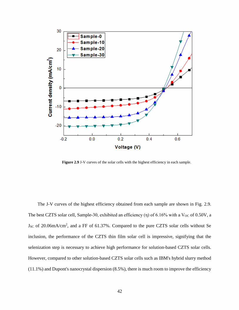
Figure 2.9 J-V curves of the solar cells with the highest efficiency in each sample. ................... 42
Figure 3.1 Schematic growth process for perovskite thin films using mixed halide sources and
method adopted from [79]. ........................................................................................................... 47
Figure 3.2 EDS spectra of the perovskite thin films. .................................................................... 49
Figure 3.3 Top-view SEM images of MAPbI3 and MAPb(I,Cl)3 thin films. ............................... 51
Figure 3.4 XRD patterns of MAPbI3 and MAPb(I,Cl)3 solar cells: (a) full range, (b) major peak at
(110) to calculate the crystal size. ................................................................................................. 53
Figure 3.5 I-V curves and parameters of MAPbI3 and MAPb(I,Cl)3 solar cells (the inset is the
efficiency distributions of 16 devices for each sample) measured at around 25℃under simulated
sunlight of 100 mW/cm2 (AM 1.5G)........................................................................................... 54
Figure 3.6 Topography AFM images (a and b), SP (c and d), and profiles of SP (e and f) of MAPbI3
(a, c, and e) and MAPb(I,Cl)3 (b, d, and f) thin films on ITO. ..................................................... 56
xii
Figure 3.7 Band alignment of devices for (a) MAPbI3 and (b)MAPb(I,Cl)3. ................................ 57
Figure 3.8 AFM images, KPFM images, and the profiles along the lines in (a) MAPbI3 and (b)
MAPb(I,Cl)3 thin films. ................................................................................................................ 59
Figure 3.9 Band diagrams around the GB in MAPbI3 and MAPb(I,Cl)3 thin films. .................... 61
Figure 3.10 The electron lifetime as a function of VOC. ............................................................... 62
Figure 3.11 Admittance spectroscopy of MAPbI3 and MAPb(I,Cl)3 solar cells: (a) Arrhenius plot
of the transition frequencies to derive the defect energy levels, (b) the distributions of the density
of the defects. ................................................................................................................................ 65
Figure 4.1 Averaged I-V curves and parameters of perovskite solar cells (10 devices for each
sample). ......................................................................................................................................... 69
Figure 4.2 SEM images of perovskite thin films deposited utilizing different purities of PbI2. (a)
99.999%, (b) 99%, and (c) 99%+Cl. (The scale bar is 1μm). ....................................................... 70
Figure 4.3 (a) XRD patterns, (b) major peak at (110), (c) transmittance, and (d) optical bandgap
energies of perovskite thin films utilizing different purities of PbI2. ............................................ 72
Figure 4.4 The electron lifetime derived from OCVD method as a function of VOC. .................. 73
Figure 4.5 Admittance spectroscopy of perovskite solar cell fabricated using low purity PbI2 with
Cl. (a) Capacitance spectra at different temperatures. (b) The derivative of the capacitance spectra
which show the transition frequency at each temperature. (c) Arrhenius plot of the transition
frequencies to derive the defect energy level. (d) The distribution of the density of the defect. .. 75
Figure 4.6 Arrhenius plots of the transition frequencies to derive the defect energy levels in
perovskite solar cells utilizing different purities of PbI2. .............................................................. 77
xiii
Figure 4.7 Defect density distributions of perovskite solar cell fabricated using different purities
of PbI2. ........................................................................................................................................... 78
Figure 5.1 Schematic device structures of (a) conventional, and (b) all inorganic CTLs perovskite
solar cells. ..................................................................................................................................... 82
Figure 5.2 AFM images of the surface of (a) Li:NiOx thin film, (b) ZnO NPs, and (c)perovskite
thin film. ........................................................................................................................................ 83
Figure 5.3 Thickness of (a) and (b) Li:NiOx thin film, (c) and (d) ZnO NPs deposited with 10 times
coating. .......................................................................................................................................... 84
Figure 5.4 J-V curves of the champion perovskite solar cell with different device structures. .... 85
Figure 5.5 Energy band diagrams of perovskite solar cells with different device structures of (a)
TiO2/spiro-OMeTAD, (b) Li:NiOx/unannealed ZnO NPs, (c) Li:NiOx/annealed ZnO NPs. ..... 87
Figure 5.6 Distributions of I–V parameters obtained from 28 perovskite solar cells with device
structure of Li:NiOx/annealed ZnO NPs. ...................................................................................... 88
Figure 5.7 Variation of the normalized I-V parameters of the perovskite solar cells with time stored
in air at room temperature without encapsulation......................................................................... 90
Figure 6.1 J-V curves of the champion perovskite solar cells with and without Al-doped ZnO NPs.
....................................................................................................................................................... 94
Figure 6.2 The statistical distributions of the Voc of perovskite solar cells with and without Al-
doped ZnO NPs. ............................................................................................................................ 96
Figure 6.3 Temperature dependence of the Voc and its linear extrapolation line to 0 K for
perovskite solar cells with and without Al-doped ZnO NPs, which helps to elucidate the dominant
recombination process in the two types of devices. ...................................................................... 97
1
INTRODUCTION
Pollution of the earth and shortage of energy sources have been the bottleneck of survival and
development for human being since the start of the 21st century. Therefore, lowering energy
consumption and protecting the environment have gradually gained attention from all over the
world. To keep sustainable development, governments, research institutes, and industries have
been fighting for the problems caused by the shortage of available energy sources. It is well known
that the best way is to exploit renewable energy resources. Solar energy is considered as the most
economic and effective among all available renewable energy resources. Solar energy is
inexhaustible and it has already been theoretically and experimentally proved that the earth would
not be polluted at all if solar energy was utilized effectively. To encourage and to promote the
direct utilization of solar energy, developed countries have been legislating and deploying solar
initiatives.
Joint Research Centre (Europe) predicted that energy directly harvested from sunlight would
be 20% of total energy consumption in 2050, and this value could be over 50% in 2100. Solar
energy will be widely utilized in industries, agriculture and daily life. Photovoltaic (PV) systems
have gained tremendous development due to intrinsic advantages as follows:
• Directly translate sunlight into electrical energy;
• Movable parts are dispensable when constructing PV systems;
• Lifetime is over 20 years without any maintenance.
2
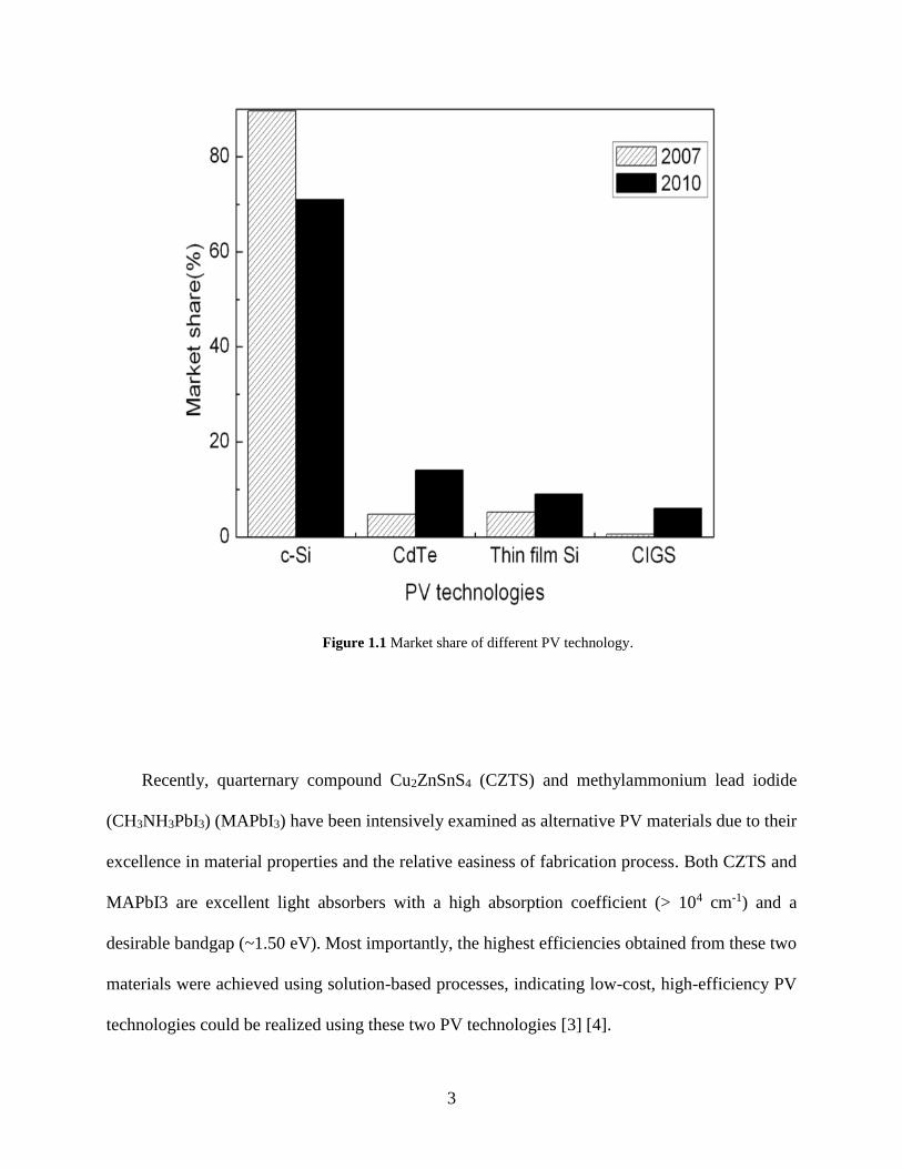
It was reported by Solarbuzz that 16.3 GW PV modules had been shipped to customers in
2010 with the lion’s share going to crystalline silicon (c-Si) technology (71%). However, market
share of thin film PV technologies has been increasing rapidly due to high cost and energy
consumption input in manufacturing c-Si PV of modules. There are three main thin film PV
technologies, CdTe, CuInxGa1-xS(Se)2 (CIGS), and thin film Si, which has gained 14%, 9%, and
6% of PV market share in 2010, respectively (Fig.1.1) [1]. Nevertheless, thin film Si solar cell has
been relatively underdeveloped due to low efficiency and instability from the Staebler–Wronski
effect. For the other two thin film technologies, there are restriction on usage of heavy metals such
as cadmium, limitations in supply for indium and tellurium, and resultant wide fluctuation in prices
of indium and tellurium. These render the combined production capacity of the existing CdTe and
CIGS technologies to lower than 100 GW per year, a small fraction of energy consumption, which
is expected to be 27 TW by 2050 [1, 2].
3
Figure 1.1 Market share of different PV technology.
Recently, quarternary compound Cu2ZnSnS4 (CZTS) and methylammonium lead iodide
(CH3NH3PbI3) (MAPbI3) have been intensively examined as alternative PV materials due to their
excellence in material properties and the relative easiness of fabrication process. Both CZTS and
MAPbI3 are excellent light absorbers with a high absorption coefficient (> 104 cm-1) and a
desirable bandgap (~1.50 eV). Most importantly, the highest efficiencies obtained from these two
materials were achieved using solution-based processes, indicating low-cost, high-efficiency PV
technologies could be realized using these two PV technologies [3] [4].
4
1.1 SOLUTION-PROCESSED THIN FILM SOLAR CELLS
1.1.1 Cu2ZnSnS4 (CZTS)
The first (I)2(II)(IV)(VI)4 solar cell was developed in 1977 by Wagner and Bridenbaugh [5]. A n-
type CdS thin film was evaporation-coated on vapor transportation-grown Cu2CdSnS4 single
crystal substrate to form the p-n junction. This device showed a short-circuit current density of 7.9
mA/cm2, an open-circuit voltage of 0.5 V, and a conversion efficiency of 1.6%. The authors
pointed out that a large series resistance limited the performance. In 1988, a heterojunction solar
cell with an open circuit voltage of 165 mV was achieved by depositing cadmium tin oxide on
CZTS thin film [6]. In 1997, the first CZTS TFSC with efficiency of 0.66% was realized by
Katagiri using electron beam deposition followed by sulfurization [7].
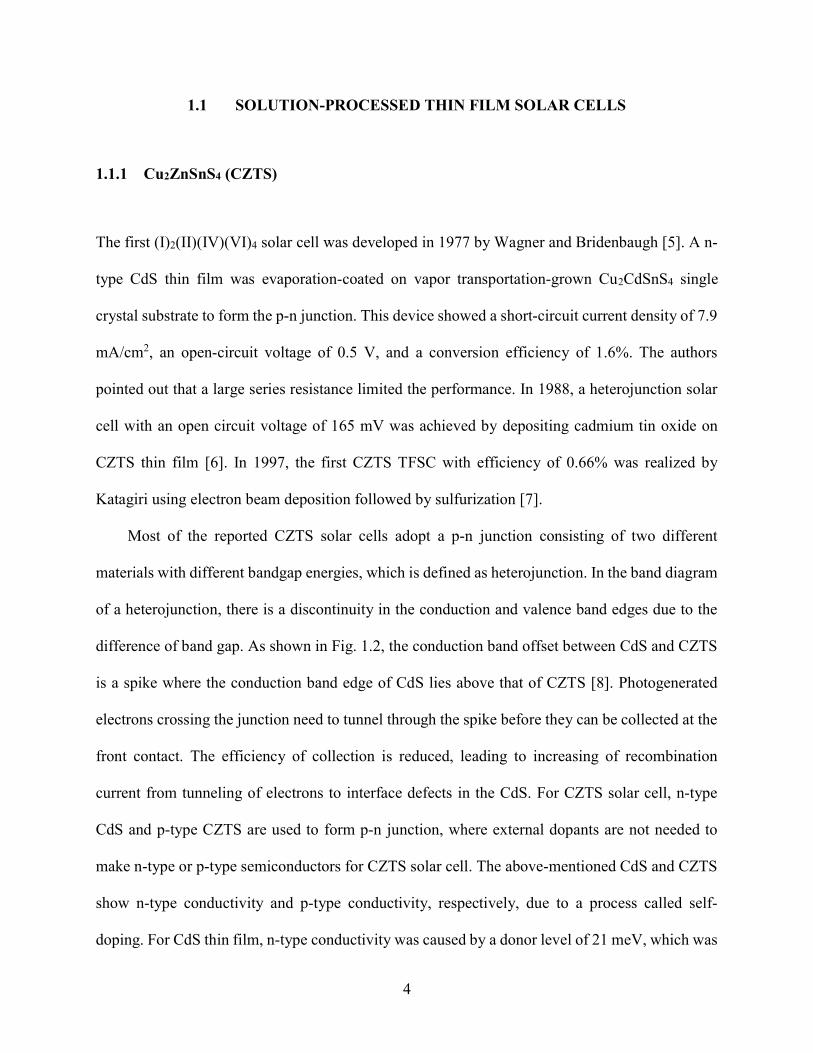
Most of the reported CZTS solar cells adopt a p-n junction consisting of two different
materials with different bandgap energies, which is defined as heterojunction. In the band diagram
of a heterojunction, there is a discontinuity in the conduction and valence band edges due to the
difference of band gap. As shown in Fig. 1.2, the conduction band offset between CdS and CZTS
is a spike where the conduction band edge of CdS lies above that of CZTS [8]. Photogenerated
electrons crossing the junction need to tunnel through the spike before they can be collected at the
front contact. The efficiency of collection is reduced, leading to increasing of recombination
current from tunneling of electrons to interface defects in the CdS. For CZTS solar cell, n-type
CdS and p-type CZTS are used to form p-n junction, where external dopants are not needed to
make n-type or p-type semiconductors for CZTS solar cell. The above-mentioned CdS and CZTS
show n-type conductivity and p-type conductivity, respectively, due to a process called self-
doping. For CdS thin film, n-type conductivity was caused by a donor level of 21 meV, which was
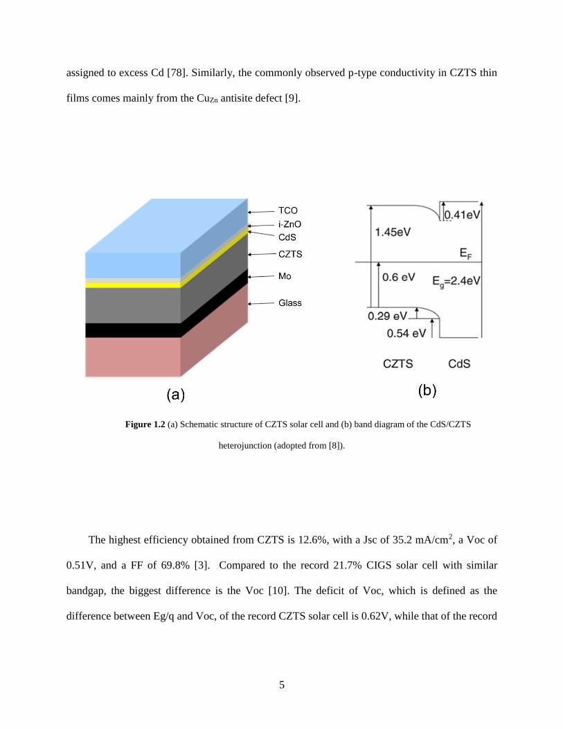
5
assigned to excess Cd [78]. Similarly, the commonly observed p-type conductivity in CZTS thin
films comes mainly from the CuZn antisite defect [9].
Figure 1.2 (a) Schematic structure of CZTS solar cell and (b) band diagram of the CdS/CZTS
heterojunction (adopted from [8]).
The highest efficiency obtained from CZTS is 12.6%, with a Jsc of 35.2 mA/cm2, a Voc of
0.51V, and a FF of 69.8% [3]. Compared to the record 21.7% CIGS solar cell with similar
bandgap, the biggest difference is the Voc [10]. The deficit of Voc, which is defined as the
difference between Eg/q and Voc, of the record CZTS solar cell is 0.62V, while that of the record
6
CIGS solar cell is 0.38V. Finding a way to improve the Voc of CZTS solar cells would
significantly increase the efficiency of CZTS solar cells.
The deficit of Voc is mainly affected by the recombination at interfaces of CdS/CZTS,
CZTS/Mo, and in the CZTS absorber layer. Polycrystalline CZTS thin film contains a large density
of intrinsic defects which is 1.0×1016 cm-3, while that of CIGS is 1.3×1014 cm-3 [11]. The large
defect density increases the density of trap states and recombination centers, resulting in the
following consequence:
• Diffusion lengths are much shorter than that of silicon wafer-based solar cells. To
increase absorption, either a strong optical absorber or multiple junctions must be used.
In the case of amorphous silicon solar cell where diffusion lengths are extremely short, p-
i-n structure is employed to extend the built-in electric field to aid carrier collection. In
the case of organic solar cell where diffusion lengths are even shorter, nanostructure and
bulk junction are employed to facilitate carrier collection.
• The presence of defect states in the band gap can limit the built-in voltage due to Fermi
level pinning. Also, the presence of defect states will lead to high dependence of minority
carrier lifetime and diffusion constant on carrier density.
• The presence of grain boundaries and other intrinsic defects increases the resistivity of
CZTS thin films, making the conductivity highly dependent on carrier density.
1.1.2 CH3NH3PbI3 (MAPbI3)
The first MAPbI3 solar cell with an efficiency of 3.81% was reported by T. Miyaska in 2009 [12].
Due to the dissolution of MAPbI3 in acetonitrile, the performance degraded quickly under
irradiation. Another nonpolar solvent, ethyl acetate, was adopted to prevent the dissolution in 2011
7
[13]. The performance of MAPbI3 solar cell was improved to 6.54%. It was mentioned that the
stability of the MAPbI3 solar cell under continued irradiation was approximately 10 min (about
80% degradation) because MAPbI3 quantum dots tends to be dissolved gradually into the redox
electrolyte. A solid hole transporting material (HTM), 2,2’,7,7’-tetrakis(N,N-di-
pmethoxyphenylamine)-9,9’-spirobifluorene (spiro-OMeTAD) was used to replace liquid
electrolyte in 2012 [14]. An efficiency of 9.7% was obtained. Furthermore, compared to the liquid
cell, the stability was remarkably improved. A sequential deposition method was developed to
deposit MAPbI3 in 2013 and a remarkable efficiency of 15.0% was achieved [15]. In the same
year, an evaporation deposition method was applied to fabricate MAPbI3 thin film [16]. The
efficiency was further improved to 15.4%. Since then, numerous groups have shifted their research
focuses to investigate MAPbI3 solar cells. The efficiency of perovskite solar cells has been
surprisingly rapidly improved from 3.8 % in 2009 [12] to 20.1% in 2015 [4]. This great advance
is mainly attributed to the rigorous efforts that worldwide research groups have been taking to
deposit high quality perovskite thin films [17-19]. The tremendous improvement can also be
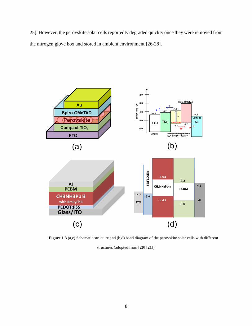
attributed to the two device structures developed for almost 20 years. One structure is based on
TiO2 as electron transport layer (ETL) and spiro-OMeTAD as hole transport layer (HTL) (Fig. 1.3
(a) and (b)) [20]. The other structure is based on organic ETL such as PCBM and organic HTL
such as poly(3,4-ethylenedioxythiophene) polystyrene sulfonate (PEDOT:PSS) and poly(3-
hexylthiophene-2,5-diyl) (P3HT) (Fig. 1.3 (c) and (d)) [21]. The perovskite thin film is deposited
in between as absorber layer to fabricate perovskite solar cells. Due to the high sensitivity of these
organic materials to moisture and oxygen, a nitrogen glove box with strict control on the
concentration of moisture and oxygen was usually used to fabricate perovskite solar cells [17, 22-
8
25]. However, the perovskite solar cells reportedly degraded quickly once they were removed from
the nitrogen glove box and stored in ambient environment [26-28].
Figure 1.3 (a,c) Schematic structure and (b,d) band diagram of the perovskite solar cells with different
structures (adopted from [20] [21]).
9
Although MAPbI3 TFSCs have evolved from the dye sensitized solar cell (DSSC) and
adopted a device structure similar to bi-layer organic solar cells, it has been found recently that
they work differently from organic solar cells [29]. The strong and abroad absorption spectrum,
the long diffusion length of minority carriers, the large two-carrier recombination rate, and the
polycrystalline structure observed in MAPbI3 thin films indicate that MAPbI3 TFSCs function
more like inorganic polycrystalline solar cells such as Cu(In,Ga)Se2 (CIGS) solar cells. The
diffusion length of CIGS thin film was estimated to be around 1μm [30]. Passivation of grain
boundaries (GBs) by sodium incorporation in polycrystalline CIGS thin film is recognized to be
one of the mechanisms for increasing the diffusion length. Similarly, it was observed that the
diffusion length of MAPbI3 solar cell was significantly increased by doping MAPbI3 thin films
with negligible amount of Cl. However, the mechanisms behind this improvement are unclear.
Admittance spectroscopy (AS) has been successfully employed to study the defect density of CIGS
and CZTS thin films [31, 32]. As mentioned earlier, polycrystalline CZTS thin film contains a
large density of intrinsic defects which is 1.0×1016 cm-3, while that of CIGS is 1.3×1014 cm-3 [11].
Similar fundamental studies should be conducted on MAPbI3 solar cells.
1.2 MOTIVATION
Most of the reported CZTS TFSCs were fabricated either by highly expensive vacuum-based
methods, or by highly toxic and flammable solvent-based methods. Fabrication process based on
low-cost nonvacuum-based methods and environmentally friendly chemicals such water is needed.
For MAPbI3 TFSCs, due to the high sensitivity of the organic charge transport layers to moisture
and oxygen, the ultimate advancement in the device stability of perovskite solar cells has yet to be
10
realized. Device structure with inorganic charge transport layers should be developed to improve
the stability of MAPbI3 TFSCs.
In addition, the research focus of CZTS and MAPbI3 TFSCs has been on development of new
fabrication methods. The working mechanisms of the devices have been rarely addressed in
literatures. Considering the solution-based method used to achieve more than 20% MAPbI3 solar
cells [4], it would be interesting to investigate the device properties of MAPbI3, such as carrier
lifetime and defect density. Not only fundamental studies on these fields are necessary to advance
the perovskite PV technologies, but also the results can be utilized as a guidance to improve the
performance of solution-processed CZTS solar cells.
1.3 CHARACTERIZATION METHODS
1.3.1 Open-Circuit Voltage Decay (OCVD)
The open-circuit voltage decay (OCVD) method was developed to measure the minority carrier
lifetime in solar cells [33]. This technique has certain advantages over frequency or steady-state-
based methods [33]. First, the lifetime as a function of VOC at high-voltage resolution can be
obtained continuously. Second, this technique does not require special treatment on samples,
which are kept undamaged during the measurement. Finally, the data processing is relatively
simple. To obtain minority carrier lifetime, only one first derivative is required.
The solar cell is initially under a constant illumination generated from a sunlight simulator
(Fig. 1.4). The VOC is continuously measured. Minority carriers are injected into the base region
during the illumination. Upon the blockage of the illumination, the VOC starts to decay due to the

11
recombination of minority carriers. To theoretically explain the mechanism, a p+-n junction, where
the conductivity of the p+-region is much greater than that of the n-region, is considered [34]. Let
pn be the hole density present in the n-region under thermal equilibrium conditions, and Δp be the
excess hole density injected due to the illumination in the n-region at the boundary of the junction
transition region. The total hole density at the junction boundary will be
𝑝 = 𝑝𝑛 + 𝛥𝑝. (2.1)
From the theory of the p-n junction, the hole density in the n-region at the junction boundary is
given by
𝑝 = 𝑝𝑛𝑒𝑞𝑉/𝑘𝑇, (2.2)
where V is the junction voltage. Combing 2.1 and 2.2, the junction voltage V can be obtained:
𝑉 = (𝑘𝑇
𝑞)𝑙𝑛(1 + (
𝛥𝑝
𝑝𝑛)). (2.3)
Assuming the excess carrier concentration, Δp, decays exponentially according to a single
effective lifetime, τe, namely,
𝛥𝑝 = 𝛥𝑝0𝑒−𝑡/𝜏𝑒, (2.4)
where 𝛥𝑝0 is the excess carrier density at the specific time when the illumination is blocked.
The junction voltage at t=0 (at the specific time when the illumination is blocked), V0, is
𝑉0 = (𝑘𝑇
𝑞)𝑙𝑛(1 + (
𝛥𝑝0
𝑝𝑛)). (2.5)
Combing 2.3 and 2.2, and 2.5, the junction voltage, or the VOC, as a function of time, t, can
be obtained from:
𝑉𝑜𝑐 = (𝑘𝑇
𝑞)𝑙𝑛(1 + (𝑒𝑞𝑉0/𝑘𝑇 − 1)𝑒−𝑡/𝜏𝑒). (2.6)
Usually 𝑞𝑉0 ≫ 𝑘𝑇 Eq. 2.6 can be simplified to
𝑉𝑜𝑐 = (𝑘𝑇
𝑞)𝑙𝑛(1 + 𝑒
𝑞𝑉0𝑘𝑇
−𝑡/𝜏𝑒). (2.7)
12
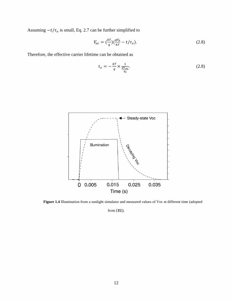
Assuming −𝑡/𝜏𝑒 is small, Eq. 2.7 can be further simplified to
𝑉𝑜𝑐 = (𝑘𝑇
𝑞)(
𝑞𝑉0
𝑘𝑇− 𝑡/𝜏𝑒). (2.8)
Therefore, the effective carrier lifetime can be obtained as
𝜏𝑒 = −𝑘𝑇
𝑞×
1𝑑𝑉𝑜𝑐
𝑑𝑡
. (2.8)
Figure 1.4 Illumination from a sunlight simulator and measured values of Voc at different time (adopted
from [35]).
13
1.3.2 Admittance Spectroscopy (AS)
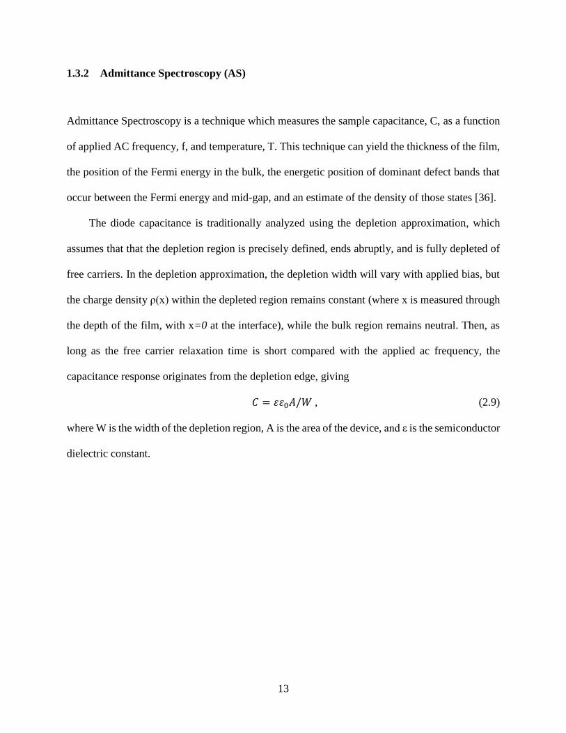
Admittance Spectroscopy is a technique which measures the sample capacitance, C, as a function
of applied AC frequency, f, and temperature, T. This technique can yield the thickness of the film,
the position of the Fermi energy in the bulk, the energetic position of dominant defect bands that
occur between the Fermi energy and mid-gap, and an estimate of the density of those states [36].
The diode capacitance is traditionally analyzed using the depletion approximation, which
assumes that that the depletion region is precisely defined, ends abruptly, and is fully depleted of
free carriers. In the depletion approximation, the depletion width will vary with applied bias, but
the charge density ρ(x) within the depleted region remains constant (where x is measured through
the depth of the film, with x=0 at the interface), while the bulk region remains neutral. Then, as
long as the free carrier relaxation time is short compared with the applied ac frequency, the
capacitance response originates from the depletion edge, giving
𝐶 = 𝜀𝜀0𝐴/𝑊 , (2.9)
where W is the width of the depletion region, A is the area of the device, and ε is the semiconductor
dielectric constant.
14
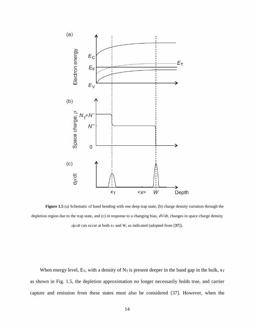
Figure 1.5 (a) Schematic of band bending with one deep trap state, (b) charge density variation through the
depletion region due to the trap state, and (c) in response to a changing bias, dV/dt, changes in space charge density
dρ/dt can occur at both xT and W, as indicated (adopted from [37]).
When energy level, ET, with a density of NT is present deeper in the band gap in the bulk, xT
as shown in Fig. 1.5, the depletion approximation no longer necessarily holds true, and carrier
capture and emission from these states must also be considered [37]. However, when the
15
temperature of the sample is too low, or the frequency applied is too high, there is no time for
carriers in the bulk to drift in and out of the depletion edge in response to the applied AC voltage.
Under this circumstance, the capacitance response will be that of the bulk dielectric,
𝐶 = 𝜀𝜀0𝐴/ℎ , (2.10)
where h is the distance between the top and back contacts. Increasing the temperature, T, or
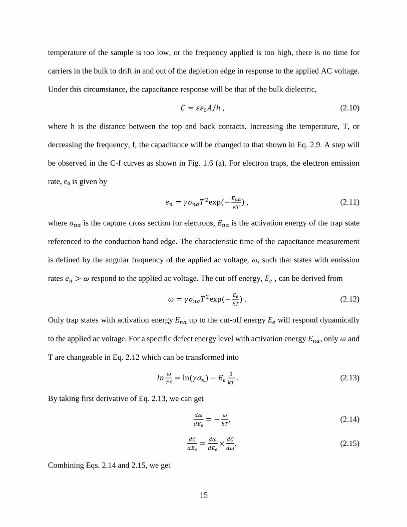
decreasing the frequency, f, the capacitance will be changed to that shown in Eq. 2.9. A step will
be observed in the C-f curves as shown in Fig. 1.6 (a). For electron traps, the electron emission
rate, en is given by
𝑒𝑛 = 𝛾𝜎𝑛𝑎𝑇2exp (−𝐸𝑛𝑎
𝑘𝑇) , (2.11)
where 𝜎𝑛𝑎 is the capture cross section for electrons, 𝐸𝑛𝑎 is the activation energy of the trap state
referenced to the conduction band edge. The characteristic time of the capacitance measurement
is defined by the angular frequency of the applied ac voltage, ω, such that states with emission
rates 𝑒𝑛 > 𝜔 respond to the applied ac voltage. The cut-off energy, 𝐸𝑒 , can be derived from
𝜔 = 𝛾𝜎𝑛𝑎𝑇2exp (−𝐸𝑒
𝑘𝑇) . (2.12)
Only trap states with activation energy 𝐸𝑛𝑎 up to the cut-off energy 𝐸𝑒 will respond dynamically
to the applied ac voltage. For a specific defect energy level with activation energy 𝐸𝑛𝑎, only 𝜔 and
T are changeable in Eq. 2.12 which can be transformed into
𝑙𝑛𝜔
𝑇2 = ln (𝛾𝜎𝑛) − 𝐸𝑒1
𝑘𝑇 . (2.13)
By taking first derivative of Eq. 2.13, we can get
𝑑𝜔
𝑑𝐸𝑒= −
𝜔
𝑘𝑇, (2.14)
𝑑𝐶
𝑑𝐸𝑒=
𝑑𝜔
𝑑𝐸𝑒×
𝑑𝐶
𝑑𝜔. (2.15)
Combining Eqs. 2.14 and 2.15, we get
16
𝑑𝐶
𝑑𝐸𝑒= −
𝜔
𝑘𝑇
𝑑𝐶
𝑑𝜔 . (2.16)
Figure 1.6 (a) Raw data of Admittance Spectroscopy for a CIGS device, (b) The Admittance Spectroscopy
data after applying Eq. (2.11), showing the characteristic (peak) frequencies at each temperature, (c) Arrhenius plot
of each peak (circles) and the linear fitting (line), (d) DLCP data (circles) in comparison of admittance spectroscopy
data (-fdC/df) data (solid line) (adopted from [37]).
17
By applying Eq. 2.16 to the admittance spectroscopy data shown in Fig. 2.3 (a), the
characteristic frequencies at each temperature can be obtained as shown in Fig. 1.6 (b). The (𝑙𝑛𝜔
𝑇2,
1
kT) data points from each peak can then be plotted on an Arrhenius plot as shown in Fig. 1.6 (c).
Using Eq. 2.13 to linearly fit the data, the slope then yields the activation energy Ena, while the
intercept can be used to derive the capture cross section σna. The trap density, Nt, versus Ee can
be obtained by rescaling the ω axis to Ee by the following equation:
𝑁𝑡 = −𝑉𝑏𝑖
𝑞𝑊
𝑑𝐶
𝑑𝜔
𝜔
𝑘𝑇 , (2.17)
where Vbi is the built-in voltage, W is the thickness of the intrinsic layer.
1.3.3 Temperature-Dependent Open-Circuit Voltage
As introduced earlier, both CZTS and MAPbI3 thin films are polycrystalline. The corresponding
PV devices are considered heterojuction solar cells since the p-n junctions in these devices form
between two different semiconductors. One diode model has been developed to describe and
analyze the J-V behaviors of these thin film solar cells [38, 39].
The forward current density of the heterojunction under illumination, J, is described by
𝐽 = 𝐽0 exp (𝑞𝑉
𝐴𝑘𝑇) − 𝐽𝑝ℎ , (2.18)
where 𝐽0 is the saturation current density of the diode, 𝐽𝑝ℎ is the photocurrent, 𝑉 is the applied
voltage, 𝐴 is the ideality factor, and 𝑘𝑇
𝑞 is the thermal voltage, a constant of 26 meV. 𝐽0 is caused
by the recombination process, which is highly temperature dependent. Therefore, 𝐽0 can be
described by
𝐽0 = 𝐽00exp (−𝐸𝑎
𝐴𝑘𝑇) , (2.19)
18
where 𝐽00 is the temperature dependent prefactor, while 𝐸𝑎 is the activation energy of the
recombination.
By combining Eq. 2.18 and 2.19, we get
𝐽 = 𝐽00exp (−𝐸𝑎
𝐴𝑘𝑇) exp (
𝑞𝑉
𝐴𝑘𝑇) − 𝐽𝑝ℎ . (2.20)
When the illuminated solar cell is short-circuited, the forward current density 𝐽 is named as short-
circuit current density, 𝐽𝑠𝑐, which is approximately equal to 𝐽𝑝ℎ:
𝐽𝑠𝑐 ≈ 𝐽𝑝ℎ . (2.21)
When the illuminated solar cell is open-circuited, the forward current density 𝐽 is zero, while the
voltage 𝑉 is named as open-circuit voltage, 𝑉𝑜𝑐, which can be expressed as:
𝑉𝑜𝑐 =𝐴𝑘𝑇
𝑞ln (
𝐽𝑝ℎ
𝐽0) . (2.22)
By combining Eq. 2.21 and 2.22, we get
𝑉𝑜𝑐 ≈𝐴𝑘𝑇
𝑞ln (
𝐽𝑠𝑐
𝐽0) . (2.23)
By combining Eq. 2.19 and 2.23, we get
𝑉𝑜𝑐 ≈𝐸𝑎
𝑞−
𝐴𝑘𝑇
𝑞ln (
𝐽00
𝐽𝑠𝑐) . (2.24)
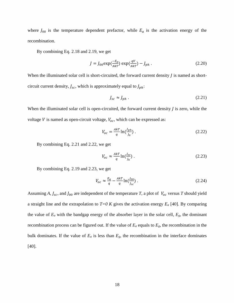
Assuming A, 𝐽𝑠𝑐, and 𝐽00 are independent of the temperature T, a plot of 𝑉𝑜𝑐 versus T should yield
a straight line and the extrapolation to T=0 K gives the activation energy Ea [40]. By comparing
the value of Ea with the bandgap energy of the absorber layer in the solar cell, Eg, the dominant
recombination process can be figured out. If the value of Ea equals to Eg, the recombination in the
bulk dominates. If the value of Ea is less than Eg, the recombination in the interface dominates
[40].
19
Figure 1.7 Temperature dependence of the open circuit voltage (VOC) and its linear extrapolation line to 0
K for the 15.2% efficient CIGS device (dashed line) and the 10.1% efficient CZTS device (solid line), which helps
to elucidate the dominant recombination process in the two types of devices [40].
1.3.4 Kelvin Probe Force Microscopy (KPFM)
KPFM is an advanced mode of atomic force microscopy (AFM) that can simultaneously measure
the local topography and SP distribution of samples with a lateral resolution in nano scales. Its
applications are widely found in semiconductor devices especially in solar cells [41-44]. In the
characterization of cross-sectional surfaces of solar cells, one of the most commonly used
techniques is to bias the solar cell with different DC voltages [44, 45]. As pointed out by Chen et
al., SP distribution within a cell under illumination in an open-circuit condition is equivalent to
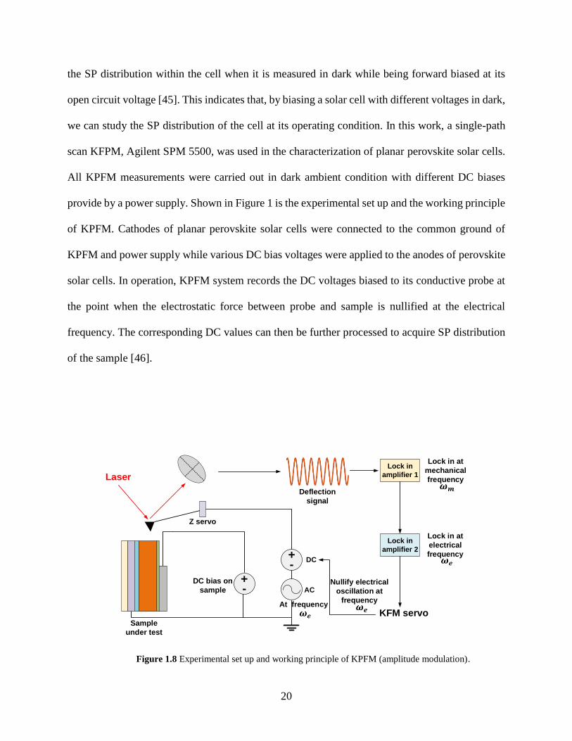
20
the SP distribution within the cell when it is measured in dark while being forward biased at its
open circuit voltage [45]. This indicates that, by biasing a solar cell with different voltages in dark,
we can study the SP distribution of the cell at its operating condition. In this work, a single-path
scan KFPM, Agilent SPM 5500, was used in the characterization of planar perovskite solar cells.
All KPFM measurements were carried out in dark ambient condition with different DC biases
provide by a power supply. Shown in Figure 1 is the experimental set up and the working principle
of KPFM. Cathodes of planar perovskite solar cells were connected to the common ground of
KPFM and power supply while various DC bias voltages were applied to the anodes of perovskite
solar cells. In operation, KPFM system records the DC voltages biased to its conductive probe at
the point when the electrostatic force between probe and sample is nullified at the electrical
frequency. The corresponding DC values can then be further processed to acquire SP distribution
of the sample [46].
Figure 1.8 Experimental set up and working principle of KPFM (amplitude modulation).
+-
+-
DC
AC
DC bias on
sample
Sample
under test
Laser
KFM servo
Z servo
Deflection
signal
Lock in
amplifier 1
Lock in
amplifier 2
Nullify electrical
oscillation at
frequency
Lock in at
mechanical
frequency
Lock in at
electrical
frequency
At frequency
21
EFFECTS OF SELENIUM VAPOR ANNEALING ON CZTS SOLAR CELLS
Kesterite Cu2ZnSn(S,Se)4, or CZTSSe, is one of the most promising materials for high-efficiency,
low-cost thin film solar cells. Efficiency of more than 12% has been reported for CZTSSe solar
cell using a hydrazine-based solution process [47]. Efficiency greater than 9% was also achieved
with CZTSSe solar cells using a coevaporation method [48]. Among various deposition techniques
for CZTSSe thin films, solution-based processes have attracted more attention than vacuum-based
methods because of their potential low cost. Significant progress has been achieved on CZTSSe
thin film solar cells using solution-based methods [49-53].
Yang et al. reported a CZTSSe solar cell, fabricated from a spin-coated hydrazine-based sol
gel, with an efficiency of 8.08% [53]. Here, a sol gel containing Cu2S, SnS2, Zn, and S was
prepared by mixing each constituent dissolved in hydrazine into final ratios of Zn/Sn = 1.2 and
Cu/(Zn + Sn) = 0.8. Additionally, Cao et al. reported a CZTSSe solar cell fabricated from a spin-
coated CZTSSe precursor ink, containing nanoparticles of Cu7S4, ZnS, and SnS dispersed in
hexanethiol [54]. The device showed an efficiency of 8.5%. Ki et al. reported an efficiency of 4.1%
from a CZTSSe solar cell fabricated using CZTSSe precursor solution [55]. The clear, light yellow
CZTSSe precursor solution contained Cu(CH3COO)2·H2O, ZnCl2, SnCl2·2H2O, and thiourea
dissolved in dimethyl sulfoxide. Most of the reported solution-based methods rely on non-aqueous
solvents such as hydrazine and organic solvents. In the case of hydrazine, toxicity and flammability
22
necessitates careful handling and extreme caution. For organic solvents, carbon is often left in the
CZTSSe thin film after annealing, a problem that degrades the solar cell’s performance.
We have recently developed a novel water-based, solution-processed method for Cu2ZnSnS4
(CZTS) thin film solar cells [56-58]. In this method, commercially available metal chlorides and
thiourea are dissolved in water to create a CZTS precursor solution which can be easily deposited
on substrates by spin-coating. The efficiency of the water-based, solution-processed CZTS solar
cell was low but promising, considering its environmental safety and potential low cost. The
performance of the water-based, solution-processed CZTS solar cell has been significantly
improved by introducing Se vapor into the annealing chamber [59].
To investigate the mechanisms behind the significant improvement brought by the
introduction of Se vapor, CZTSSe thin films and solar cells were obtained from CZTS precursor
thin films. These were deposited by a water-based method and annealed with Se vapor for varied
durations. The morphological, structural, compositional, and optical properties of CZTSSe thin
films were examined. The correlation of CZTSSe solar cell performance with different processing
conditions was also investigated.
2.1 EXPERIMENTAL PROCEDURES
2.1.1 Materials
Copper(II) chloride dihydrate (99.99%), zinc chloride (99.99%), tin(II) chloride dihydrate
(99.99%), thiourea (99.0%), selenium powder (99.99%), and ethanol (99.5%) were purchased
23
from Sigma Aldrich and used directly without further purification. Deionized water (DI-water) (16
MΩ) was produced in an in-house system.
2.1.2 CZTS Precursor Solution Preparation
The coating solution was prepared by dissolving copper(II) chloride dihydrate (1.12 mmol), zinc
chloride (0.75 mmol), tin(II) chloride dihydrate (0.75 mmol), and thiourea (6 mmol) into a mixture
solution containing DI-water (2 ml) and ethanol (1ml) at room temperature. A clear solution was
obtained after stirring at room temperature for 20 min.
2.1.3 CZTS Precursor Thin Film Preparation
The CZTS precursor solution was spin-coated on low alkaline glass substrates and Mo-coated low
alkaline glass substrates. The scanning electron microscopy (SEM) images, optical properties, and
Raman spectra of CZTS thin films were obtained from the samples deposited on low alkaline glass
substrates. X-ray diffraction (XRD) patterns and device fabrication were conducted using the
samples deposited on Mo-coated low alkaline glass substrates. Drying at 110 ℃ in air evaporated
the solvents in the as-coated films. Pre-annealing at 250 ℃ in a N2-filled tube furnace decomposed
CZTS precursors for generating metal sulfides (copper sulfide, zinc sulfide, and tin sulfide)
nanocrystals. The spin-coating and drying processes as well as pre-annealing were repeated several
times to deposit CZTS thin films with designated thickness.
24
2.1.4 CZTS Thin Film Preparation
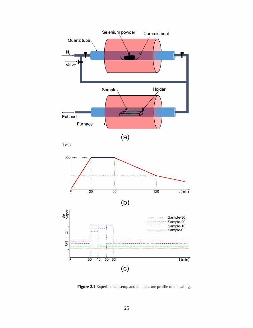
The pre-annealed CZTS precursor thin films were placed in a tube furnace. A ceramic box
containing Se powder was placed in a separate tube furnace to generate Se vapor; this vapor was
simultaneously transported by N2 flow to the annealing tube furnace (Fig. 2.1(a)). The temperature
of the tube furnace was raised to 550 ℃ to grow CZTS polycrystalline thin films (Fig. 2.1(b)). The
growth was allowed for 30 min as determined by our optimization tests. The amounts of Se
incorporated into the CZTS thin films were controlled by changing the time of introducing Se
vapor (Sample-0: no Se vapor was applied, Sample-10: Se vapor was applied for 10 min, Sample-
20: Se vapor was applied for 20 min, Sample-30: Se vapor was applied for 30 min) (Fig. 2.1(c)).
After cooling under the protection of N2, CZTS samples were immediately transferred to a
vacuum-connected dessicator for later use.
25
Figure 2.1 Experimental setup and temperature profile of annealing.
26
2.1.5 Device Fabrication
The CZTS devices were completed using a similar structure as conventional CIGS solar cells [60].
CdS, intrinsic ZnO (i-ZnO), indium-doped tin oxide (ITO), and Ag electrodes were sequentially
deposited on CZTS thin films. CdS was coated on the CZTS thin film by chemical bath deposition
(CBD). The CZTS samples were vertically inserted into a beaker containing aqueous solution of
CdI2 (1.4 mM), CS(NH2)2 (0.14 M), and NH4OH (1 M). The solution was heated to 60 ℃, and the
reaction was kept for 12 min. Samples were taken out and cleaned in DI-water. The coating
procedures needed to be repeated once to grow CdS thin film with a total thickness of 50 nm. RF
sputtering was then used to deposit 60 nm of i-ZnO and 200 nm of ITO. Electron beam evaporation
was applied to deposit the Ag electrode with a thickness of 200 nm through a shadow mask. Four
CZTS solar cells on each sample were fabricated after mechanical scribing.
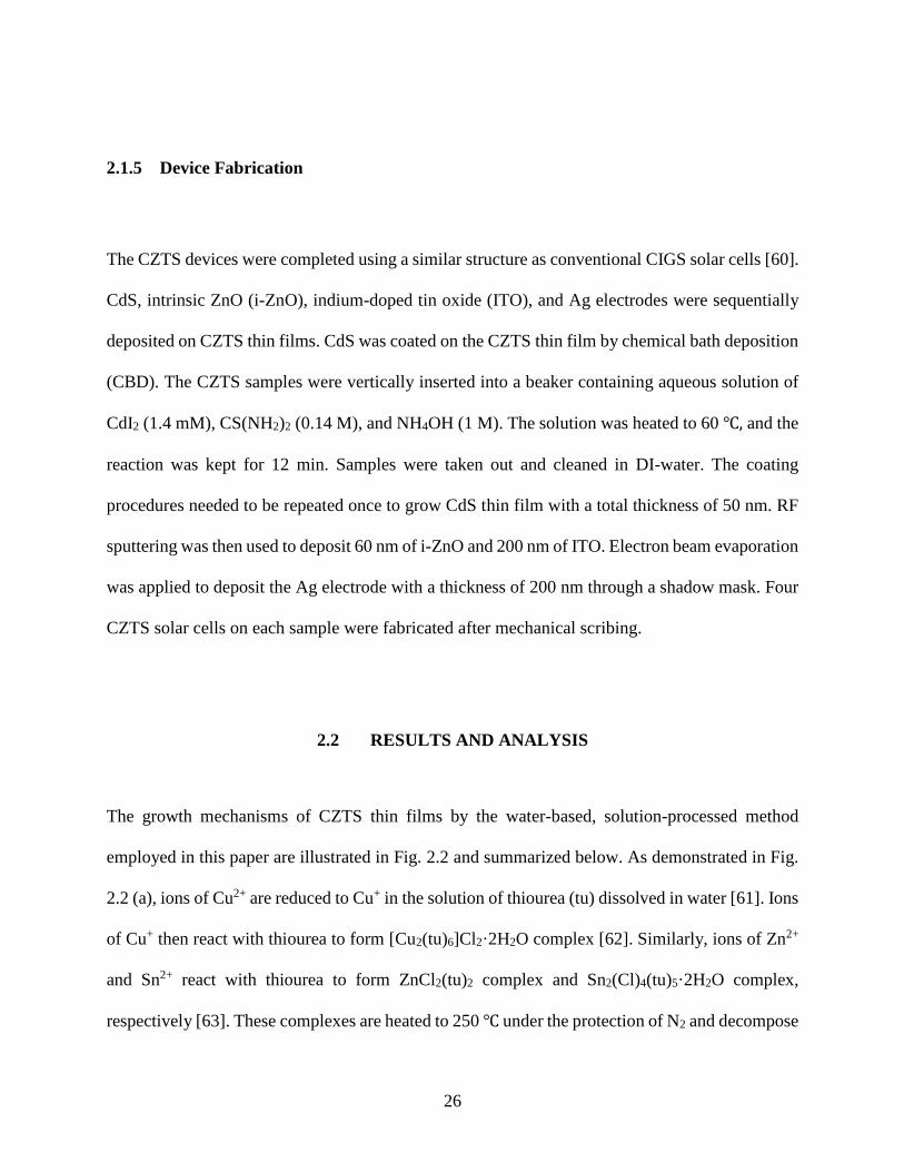
2.2 RESULTS AND ANALYSIS
The growth mechanisms of CZTS thin films by the water-based, solution-processed method
employed in this paper are illustrated in Fig. 2.2 and summarized below. As demonstrated in Fig.
2.2 (a), ions of Cu2+ are reduced to Cu+ in the solution of thiourea (tu) dissolved in water [61]. Ions
of Cu+ then react with thiourea to form [Cu2(tu)6]Cl2·2H2O complex [62]. Similarly, ions of Zn2+
and Sn2+ react with thiourea to form ZnCl2(tu)2 complex and Sn2(Cl)4(tu)5·2H2O complex,
respectively [63]. These complexes are heated to 250 ℃ under the protection of N2 and decompose
27
into volatile products such as COS, CS2, NH2CN, HNCS, NH3, HCN, HCl, SO2, and metal sulfide
nanoparticles. These volatile products are discharged from the samples with the flow of N2. Lastly,
samples mainly containing copper sulfide, zinc sulfide, and tin sulfide nanoparticles are annealed
at 550 ℃ in N2. These metal sulfide nanoparticles react to grow polycrystalline CZTS thin films
in the presence of Se vapor [64].
Figure 2.2 Growth mechanisms of CZTS thin films.
28
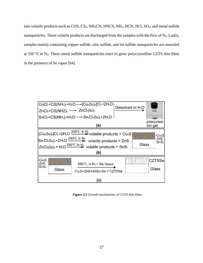
Table 2.1 Chemical composition of the final CZTS thin film.
Sample Cu/(Zn+Sn) Zn/Sn Se/(S+Se)
Pre-annealed 0.83 1.12 0
Sample-0 0.88 1.24 0
Sample-10 0.84 1.30 0.08
Sample-20 0.90 1.27 0.19
Sample-30 0.81 1.28 0.25
For the study on the influence of Se vapor feeding, four CZTS precursor thin film samples
(pre-annealed) were prepared. The compositions of the pre-annealed and annealed samples were
analyzed using EDX and summarized in Table 2.1. The elemental ratios in the pre-annealed sample
were carefully controlled by changing the concentrations of raw materials in the CZTS precursor
solution. Subsequently, the ratios of Cu/(Zn+Sn) and Zn/Sn were comparable to those reported in
highly performed CZTS solar cells [47, 48]. All annealed samples were copper-poor, zinc-rich,
which is beneficial to compress the formation of binary phases such as Cu2S, and to generate self-
doped p-type conductivity in CZTS thin films [65]. The ratios of Cu/(Zn+Sn) and Zn/Sn were
slightly increased compared to those of pre-annealed sample due to the loss of Sn. The depletion
of Sn was not severe because the annealing process was conducted in atmospheric pressure, which
helps to minimize the loss of Sn as suggested in literatures [66, 67]. The ratio of Se/(Se+S) was
increased by prolonging the Se vapor time during annealing, indicating more atoms of S were
replaced by those of Se in CZTS crystals grown with longer Se vapor introducing time. A generally
increasing trend in the loss of Sn was observed when the Se vapor introducing duration was
increased. This can be attributed to the increase of Se concentration as suggested by P. Salomé et
al. who reported that more Se incorporation into CZTS thin films promotes formation of Se
compounds and therefore promotes the evaporation of Sn over Zn [66].
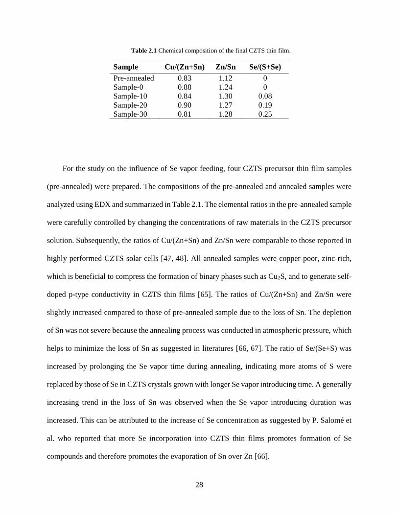
29
Figure 2.3 Surface (a~e) and cross section (f~j) SEM images of pre-annealed and annealed CZTS thin
films (a & f, Pre-annealed; b & g, Sample-0; c & h, Sample-10; d & i, Sample-20; and e & j, Sample-30) (the scale
bar is 1 μm).
30
To suppress the loss of Sn, it was suggested that the deposition of CZTS thin films should be
conducted at temperatures below 550 °C and a following annealing step should be applied in an
inert gas atmosphere to improve crystal quality [68]. Also, introducing vapor of SnS2 into the
annealing chamber was proven to be effective to reduce the loss of Sn [69]. However, it remains
unresolved to what extent the loss of Sn could be endured without detrimental effects on the
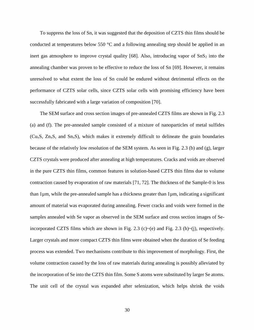
performance of CZTS solar cells, since CZTS solar cells with promising efficiency have been
successfully fabricated with a large variation of composition [70].
The SEM surface and cross section images of pre-annealed CZTS films are shown in Fig. 2.3
(a) and (f). The pre-annealed sample consisted of a mixture of nanoparticles of metal sulfides
(CuxS, ZnxS, and SnxS), which makes it extremely difficult to delineate the grain boundaries
because of the relatively low resolution of the SEM system. As seen in Fig. 2.3 (b) and (g), larger
CZTS crystals were produced after annealing at high temperatures. Cracks and voids are observed
in the pure CZTS thin films, common features in solution-based CZTS thin films due to volume
contraction caused by evaporation of raw materials [71, 72]. The thickness of the Sample-0 is less
than 1µm, while the pre-annealed sample has a thickness greater than 1µm, indicating a significant
amount of material was evaporated during annealing. Fewer cracks and voids were formed in the
samples annealed with Se vapor as observed in the SEM surface and cross section images of Se-
incorporated CZTS films which are shown in Fig. 2.3 (c)~(e) and Fig. 2.3 (h)~(j), respectively.
Larger crystals and more compact CZTS thin films were obtained when the duration of Se feeding
process was extended. Two mechanisms contribute to this improvement of morphology. First, the
volume contraction caused by the loss of raw materials during annealing is possibly alleviated by
the incorporation of Se into the CZTS thin film. Some S atoms were substituted by larger Se atoms.
The unit cell of the crystal was expanded after selenization, which helps shrink the voids
31
commonly encountered in solution-based deposition methods. Another explanation is that Se is a
better vapor-transport agent than S for this material system, which might have a more dramatic
effect on grain growth than the expansion of the unit cell. This hypothesis is supported by the
results reported by S. Riha et al. who deposited CZTS thin films by annealing pure CZTS
nanocrystals and Se-rich CZTS nanocrystals coated on substrates [73]. It was found that no
transport was observed during annealing for pure CZTS nanocrystal films; however, in some cases
of Se-rich CZTS films, material was completely transported off the substrate into the quartz tube.
These results indicate that introducing Se vapor into the annealing chamber helps enhance the
grain growth of CZTS thin films.
32
Figure 2.4 XRD patterns of CZTS thin films. The standard XRD patterns for CZTSSe and CZTS are
shown above.
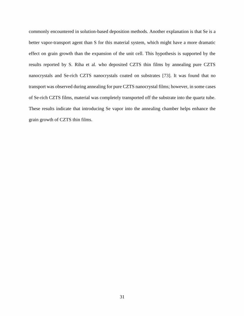
The XRD patterns of the samples together with the standard pattern of CZTSe (JCPDS 52-
0868) and CZTS (JCPDS 26-0575) are presented in Fig. 2.4. For sample-0, the diffraction peaks
can be indexed to those of kesterite CZTS which has a tetragonal structure with three major peaks
of (112), (204), and (312). The diffraction peaks of the samples annealed with Se vapor present
shift to lower values of 2θ and move closer to those of CZTSe. As the Se vapor introducing
duration was extended, more S atoms (1.84 Å) were replaced by larger Se atoms (1.98 Å), leading
to an increase in the lattice constant.
33
Figure 2.5 Raman spectra of pre-annealed and annealed CZTSSe thin films.
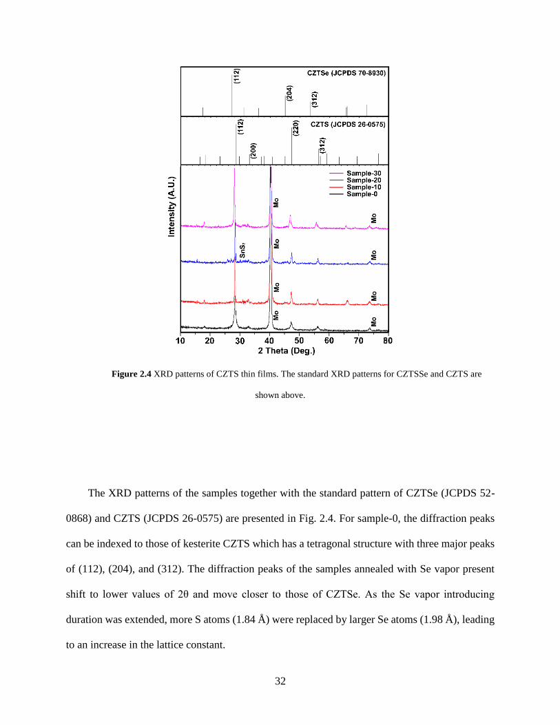
The Raman scattering spectra of pre-annealed samples and samples annealed with Se vapor
are plotted in Fig. 2.5. Pre-annealed samples exhibited a prominent peak at 318cm-1 that was
assigned to SnS2. This pattern is highly similar to what was observed for a multilayer of
Cu2S/SnS2/ZnS deposited using atomic layer deposition, indicating that the pre-annealed sample
mainly consists of a mixture of nanoparticles of metal sulfides as observed in the SEM images
[74]. After annealing in N2 at 550 °C for 30 min without Se vapor, the main peak shifted to 337
cm-1, and another peak at 287 cm-1 was also observed. However, peaks of some secondary phases
34
such as SnxS and CuxS were also observed as shown in Fig. 4.4 [75, 76]. A peak at 470 cm-1 in
Sample-20 can be assigned to CuxS [77]. This is associated with the fact that Sample-20 had the
highest ratio of Cu/(Zn+Sn); a high concentration of Cu resulted in phase precipitation in the form
of CuxS. For the annealed samples with Se vapor, two main peaks originated from CZTS, shifted
towards each other and following the same trend as reported for CZTS with an intermediate S/Se
ratio [78].
Secondary phases in CZTS thin films are detrimental to the performance of CZTS solar cells.
Firstly, secondary phases such as ZnS have a much larger band gap than CZTS. The large
difference in band gap will lead to a mismatch in energy levels of the valence band and conduction
band. Internal barriers between secondary phases and CZTS will be formed, which is expected to
degrade the performance of the PV device. Secondly, the density of grain boundaries will be
increased due to the segregation of secondary phases from the CZTS phase in the polycrystalline
thin film absorber layer. The recombination occurring at the grain boundaries is consequently
intensified, leading to degraded PV device parameters, such as short-circuit current density (JSC)
and fill factor (FF). Lastly, the presence of CuxS in CZTS thin films will facilitate the formation
of shorting paths in the absorber layer between the front contact and the back contact due to the
commonly observed high conductivity of CuxS [79]. As a result, the JSC will be significantly
decreased. Strategies have been proposed to eliminate secondary phases in CZTS thin films. The
first proposal is to strictly control the CZTS thin film composition. One study conducted on the
phase diagram of the Cu2S–ZnS–SnS2 system by I. Olekseyuk et al. revealed that CZTS only
existed in this system as a single phase over a very narrow range of composition varying no more
than ±1.5 % absolute from the stoichiometric values for each element [80]. Any large deviation
from the stoichiometric values will result in formation of secondary phases. This gives an
35
explanation to why the secondary phases were widely detected in CZTS thin films grown by
different methods. Since the elimination of secondary phases during growth of CZTS thin film is
extremely difficult, chemical routes have been developed to remove secondary phases after the
deposition of CZTS thin films. M. Bar et al. reported that the surface composition of CZTS thin
films was significantly altered after KCN etching was applied [79]. This alteration in composition
mainly comes from a preferred etching of Cu and, to a lesser degree, Sn. A less toxic chemical
approach based on HCl was developed to selectively etch Zn-rich secondary phases on the surface
of CZTS thin films [81]. This etching process demonstrated a significant impact on the
performance of the solar cells by increasing the JSC and decreasing the series resistance, RS. Similar
approaches are being explored for the CZTS thin films deposited using the same process as
reported in this work. Results will be reported elsewhere.
36
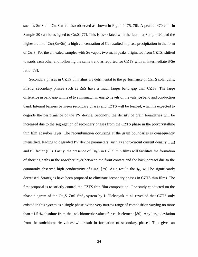
Figure 2.6 (ahν)2 of the annealed CZTS thin films as a function of hν.
The bandgaps were determined by linearly extrapolating (ahν)2 versus photon energy (hν)
(Fig. 2.6). Sample-0 had a bandgap of 1.47 eV, a value close to those reported in literatures
concerning pure CZTS thin films [82]. For three Se-included CZTS samples, the band gaps were
1.42, 1.34, and 1.28eV, respectively, showing a decreasing trend as the Se vapor introducing time
was lengthened. The narrowing of the bandgap partly originated from the enhancement of crystal
size when more Se atoms were incorporated into the CZTS thin film to facilitate the growth of
crystal. Nevertheless, to a large extent, the decrease of the bandgap was a result of the unit cell
expansion due to the substitution of S atoms in CZTS by Se atoms. Although no definite conclusion
37
has been made in literature about the effects of Se inclusion on the optical bandgap of CZTS thin
films and nanoparticles as presented earlier, further increasing the concentration of Se is expected
to reduce the bandgap of CZTS thin film. A value of ~1.5 eV has been reported on the bandgap of
pure CZTS thin films deposited by different methods. While discrepancies on the bandgap of pure
CZTSe thin films exist in literature, a value of ~1.0 eV has been widely recognized on the bandgap
of pure CZTSe thin films deposited by different methods [82, 83]. It was suggested that the
existence of some secondary phases such as ZnSe were the possible reason for the difference in
overall bandgap of CZTSe thin films. A simple model to determine the relationship between the
ratio of Se/(Se+S) and the bandgap of CZTS nanoparticle was adopted by H. Wei et al. from the
model developed by M. Bär et al. to derive the optical bandgap for penternary
Cu(In1−xGax)(SySe1−y)2 (CIGSSe) alloys from its Ga/(Ga+In) ratio as well as from its S/(S+S) ratio
[84, 85]. The model is extended to determine the optical bandgaps for penternary CZTSSe alloys,
𝐸𝑔𝐶𝑍𝑇𝑆𝑆𝑒, from its Se/(Se+S) ratio using the linear approximation between the bandgap of the pure
CZTS, 𝐸𝑔𝐶𝑍𝑇𝑆, and the bandgap of the pure CZTSe, 𝐸𝑔
𝐶𝑍𝑇𝑆𝑒:
𝐸𝑔𝐶𝑍𝑇𝑆𝑆𝑒(𝑥) = (1 − 𝑥)𝐸𝑔
𝐶𝑍𝑇𝑆 + 𝑥𝐸𝑔𝐶𝑍𝑇𝑆𝑒 − 𝑏𝑥(1 − 𝑥), (4.1)
which is corrected by the alloy specific “optical bowing constant” b. Assumption of a band gap
value of 1.5eV for CZTS and 1.0eV for CZTSe was applied in the calculation. The bandgaps
derived from the transmittance data were used to calculate the constant b which varied from 0.4 to
0.5. Therefore, different values of b (0.4 and 0.5) were applied in the calculation of the bandgaps
for CZTS with a Se/(Se+S) ratio changing from 0 to 1.
38
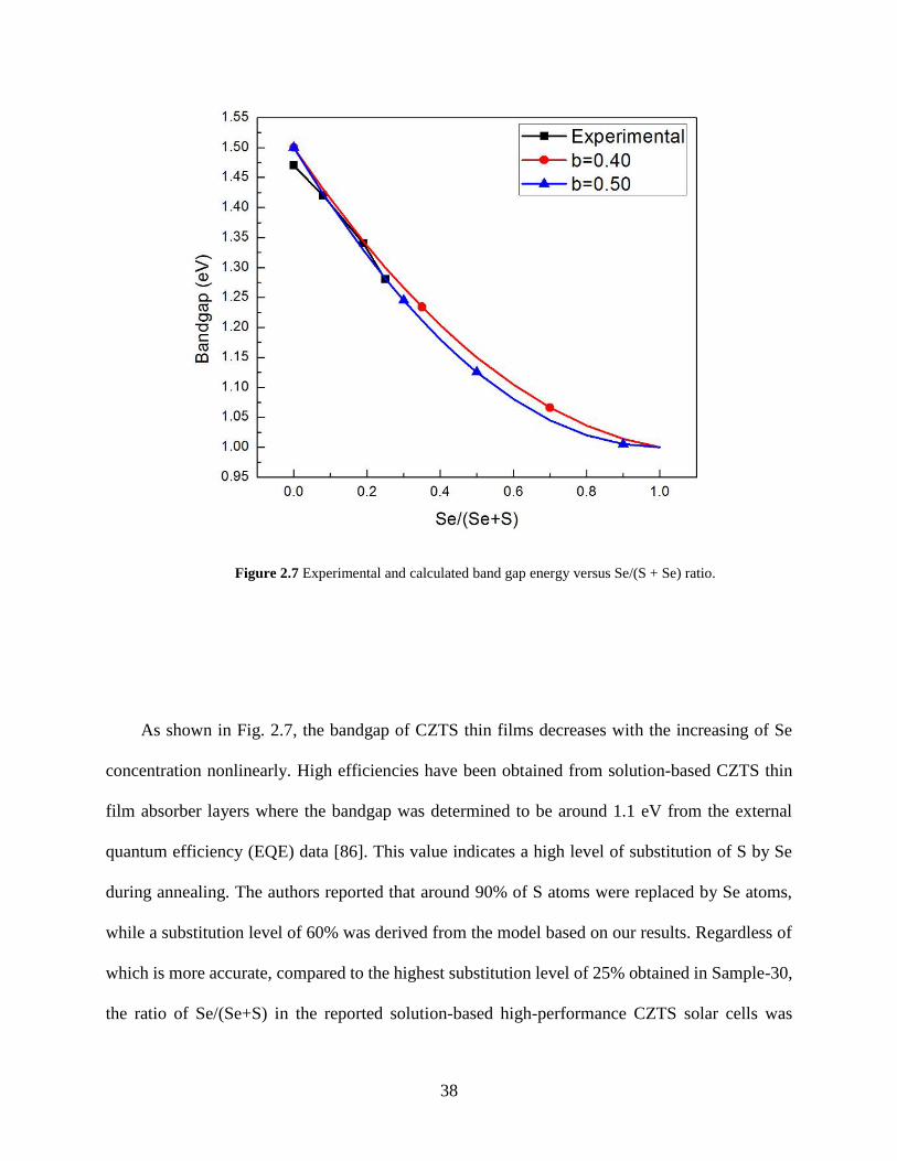
Figure 2.7 Experimental and calculated band gap energy versus Se/(S + Se) ratio.
As shown in Fig. 2.7, the bandgap of CZTS thin films decreases with the increasing of Se
concentration nonlinearly. High efficiencies have been obtained from solution-based CZTS thin
film absorber layers where the bandgap was determined to be around 1.1 eV from the external
quantum efficiency (EQE) data [86]. This value indicates a high level of substitution of S by Se
during annealing. The authors reported that around 90% of S atoms were replaced by Se atoms,
while a substitution level of 60% was derived from the model based on our results. Regardless of
which is more accurate, compared to the highest substitution level of 25% obtained in Sample-30,
the ratio of Se/(Se+S) in the reported solution-based high-performance CZTS solar cells was
39
undoubtedly higher, indicating that further incorporation of Se can be achieved by adjusting the
annealing process. The bandgap of CZTS thin films can be conveniently tuned, and the growth of
CZTS crystals will be enhanced, which is expected to improve the performance of CZTS thin film
solar cells.
Figure 2.8 I-V parameters of CZTSSe solar cells.
40
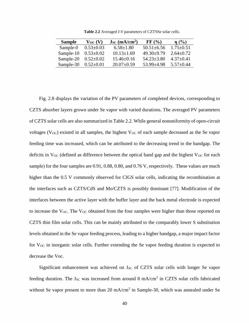
Table 2.2 Averaged I-V parameters of CZTSSe solar cells.
Sample VOC (V) JSC (mA/cm2) FF (%) η (%)
Sample-0 0.53±0.03 6.58±1.80 50.51±6.56 1.75±0.51
Sample-10 0.53±0.02 10.13±1.69 49.30±9.79 2.64±0.72
Sample-20 0.52±0.02 15.46±0.16 54.23±3.80 4.37±0.41
Sample-30 0.52±0.01 20.07±0.59 53.99±4.98 5.57±0.44
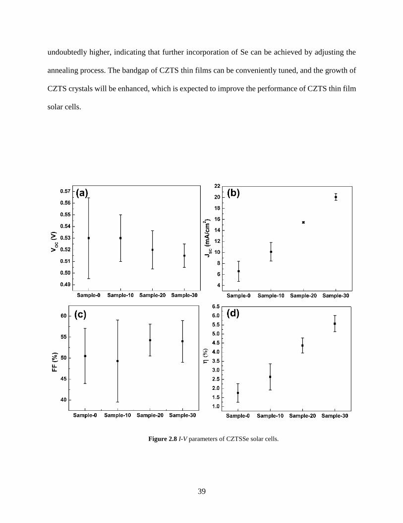
Fig. 2.8 displays the variation of the PV parameters of completed devices, corresponding to
CZTS absorber layers grown under Se vapor with varied durations. The averaged PV parameters
of CZTS solar cells are also summarized in Table 2.2. While general nonuniformity of open-circuit
voltages (VOC) existed in all samples, the highest VOC of each sample decreased as the Se vapor
feeding time was increased, which can be attributed to the decreasing trend in the bandgap. The
deficits in VOC (defined as difference between the optical band gap and the highest VOC for each
sample) for the four samples are 0.91, 0.88, 0.80, and 0.76 V, respectively. These values are much
higher than the 0.5 V commonly observed for CIGS solar cells, indicating the recombination at
the interfaces such as CZTS/CdS and Mo/CZTS is possibly dominant [77]. Modification of the
interfaces between the active layer with the buffer layer and the back metal electrode is expected
to increase the VOC. The VOC obtained from the four samples were higher than those reported on
CZTS thin film solar cells. This can be mainly attributed to the comparably lower S substitution
levels obtained in the Se vapor feeding process, leading to a higher bandgap, a major impact factor
for VOC in inorganic solar cells. Further extending the Se vapor feeding duration is expected to
decrease the Voc.
Significant enhancement was achieved on JSC of CZTS solar cells with longer Se vapor
feeding duration. The JSC was increased from around 8 mA/cm2 in CZTS solar cells fabricated
without Se vapor present to more than 20 mA/cm2 in Sample-30, which was annealed under Se
41
vapor for 30 min. Although the red shift of the onset wavelength and the higher absorption
coefficients seen in the absorbance of Sample-30 contributed to the increase of JSC, the
improvement on the optical properties alone is not likely to significantly boost the JSC. The
enhancement in crystal size and the passivation of the grain boundaries by Se-rich surfaces are
most likely the two critical driving forces for JSC. The former helps improve JSC in a way that the
recombination is reduced due to lower the density of grain boundaries associated with large grain
domains. The latter leads to a lower bandgap surface layer where the potential barriers are removed
for grain-grain carrier transport. Similar to the nonuniformity in VOC, the FF was also widely
distributed. This was partly caused by the nonuniformity of CdS deposited on CZTS thin film. The
size of the samples used in this work was 1''×1'', while the volume of the solution where CdS was
deposited was 150 ml. Upgrading of the CBD setup is expected to fabricate CZTS solar cells with
more uniform PV parameters. The highest FF of each sample increased with greater Se introducing
times. This is partly related to the series and shunting resistances since the electrical properties of
the CZTS thin films are highly dependent on the ratio of Se/(Se+S). Mainly due to the significant
improvement of JSC, the CZTS solar cells obtained from the CZTS thin films annealed with Se
vapor showed remarkably improved efficiencies.
42
Figure 2.9 J-V curves of the solar cells with the highest efficiency in each sample.
The J-V curves of the highest efficiency obtained from each sample are shown in Fig. 2.9.
The best CZTS solar cell, Sample-30, exhibited an efficiency (η) of 6.16% with a VOC of 0.50V, a
JSC of 20.06mA/cm2, and a FF of 61.37%. Compared to the pure CZTS solar cells without Se
inclusion, the performance of the CZTS thin film solar cell is impressive, signifying that the
selenization step is necessary to achieve high performance for solution-based CZTS solar cells.
However, compared to other solution-based CZTS solar cells such as IBM's hybrid slurry method
(11.1%) and Dupont's nanocrystal dispersion (8.5%), there is much room to improve the efficiency
43
[54, 86]. Three more issues could be readily addressed to further improve the efficiency of the
water-based, solution-processed CZTS solar cell. Firstly, diffusion of sodium from soda lime glass
was also found to profoundly affect grain size, crystal texture, and conductivity of CZTS thin films.
Replacing the low alkaline glass substrates used in this work with soda lime glass substrates may
further improve the performance of CZTS solar cells [87]. Secondly, the layers of CdS and ZnO
were prepared using process parameters optimized for CIGS solar cells [60]. Optimization of these
layers will possibly further improve the performance of CZTS solar cells. Lastly, while further
extending the Se vapor feeding duration could enhance the incorporation of Se into CZTS thin
films and presumably lead to higher efficiency, it is difficult to be realized at this stage because
the total annealing time of 30 min is the presently optimized. This must be done in conjunction
with the modification of other process parameters, such as lowering the annealing temperature and
increasing the Se vapor pressure. Corresponding experiments are under way and expected to
fabricate CZTS thin film solar cells with higher efficiencies.
44
EFFECTS OF CHLORINE DOPING ON MAPBI3 SOLAR CELL
Methylammonium lead halide perovskites have emerged as promising photovoltaic (PV) materials
because of their excellent optical properties such as high absorption coefficients for a broad range
of sunlight absorption. Also, the abundance of raw materials and the ability of being solution
processed make methylammonium lead halide perovskites more suitable for low cost PV
technologies. High power conversion efficiencies of more than 15% have been reported from both
mesoporous structure devices and planar structure devices. The planar structure devices are more
advantageous than the mesoporous structure devices because high temperature annealing
necessary for mesorporous structure is not required for planar structure devices. Thus, low
temperature processing, which is suitable for plastic solar cells, can be applied to fabricate
methylammonium lead halide perovskite solar cells. Conversion efficiency over10% has been
reported for methylammonium lead halide perovskite solar cell fabricated on plastic substrates.
So far, two processes have been developed to fabricate planar perovskite solar cells. The
first process is called one-step process where metal halide is mixed with methylammonium iodide
and the as-synthesized methylammonium lead halide perovskite is spin-coated on substrates. The
other process is called two-step process where metal halide is spin-coated on substrates and
methylammonium lead halide perovskite is formed by inserting the substrates into
methylammonium iodide solution. In one-step process, two metal halides, lead iodide (PbI2) and
lead chloride (PbCl2), have been commonly used to synthesize methylammonium lead halide
45
perovskites which are denoted as MAPbI3 and MAPb(I,Cl)3, respectively, with MAPb(I,Cl)3 solar
cells leading the performance due to its long diffusion length of carriers. Nevertheless, it is
extremely difficult to control the morphology of perovskite thin films because it is significantly
affected by the environment of one-step process. In two-step process, the morphology of
perovskite thin film is very uniform. However, PbI2 has been exclusively used because the
solubility of PbCl2 is extremely low. Therefore, the advantages associated with Cl incorporation
cannot be taken.
3.1 EXPERIMENTAL PROCEDURES
3.1.1 Synthesis of CH3NH3I (MAI) and CH3NH3Cl (MACl)
MAI and MACl were synthesized according to a reported procedure [88]. MAI was synthesized
by reacting 30 mL of methylamine (40 % in methanol, TCI) and 32.3 mL of hydroiodic acid (57
wt% in water, Aldrich) in an ice bath for 2 h with stirring. The precipitate was collected through
removing the solvents by a rotary evaporator. The as-obtained product was washed three times
with diethyl ether, and then recrystallized from a mixed solvent of diethyl ether and ethanol. After
filtration, the final MAI was collected and dried at 60 °C in a vacuum oven for 24 h. MACl was
synthesized by reacting 30 mL of methylamine (40 % in methanol, TCI) and 20.4 mL of
hydrochloric acid (37 wt% in water, Aldrich) in an ice bath for 2 h with stirring. The precipitation
and collection of MACl was carried out using as same procedures as used for MAI.
46
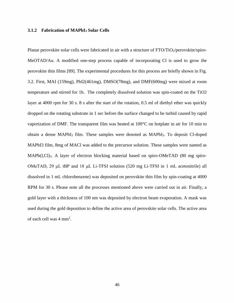
3.1.2 Fabrication of MAPbI3 Solar Cells
Planar perovskite solar cells were fabricated in air with a structure of FTO/TiO2/perovskite/spiro-
MeOTAD/Au. A modified one-step process capable of incorporating Cl is used to grow the
perovskite thin films [89]. The experimental procedures for this process are briefly shown in Fig.
3.2. First, MAI (159mg), PbI2(461mg), DMSO(78mg), and DMF(600mg) were mixed at room
temperature and stirred for 1h. The completely dissolved solution was spin-coated on the TiO2
layer at 4000 rpm for 30 s. 8 s after the start of the rotation, 0.5 ml of diethyl ether was quickly
dropped on the rotating substrate in 1 sec before the surface changed to be turbid caused by rapid
vaporization of DMF. The transparent film was heated at 100°C on hotplate in air for 10 min to
obtain a dense MAPbI3 film. These samples were denoted as MAPbI3. To deposit Cl-doped
MAPbI3 film, 8mg of MACl was added to the precursor solution. These samples were named as
MAPb(I,Cl)3. A layer of electron blocking material based on spiro-OMeTAD (80 mg spiro-
OMeTAD, 29 μL tBP and 18 μL Li-TFSI solution (520 mg Li-TFSI in 1 mL acetonitrile) all
dissolved in 1 mL chlorobenzene) was deposited on perovskite thin film by spin-coating at 4000
RPM for 30 s. Please note all the processes mentioned above were carried out in air. Finally, a
gold layer with a thickness of 100 nm was deposited by electron beam evaporation. A mask was
used during the gold deposition to define the active area of perovskite solar cells. The active area
of each cell was 4 mm2.
47
Figure 3.1 Schematic growth process for perovskite thin films using mixed halide sources and method
adopted from [89].
3.1.3 Characterization
A UV-visible spectrometer (Agilent 8453) was used to obtain the transmittance (T) of CZTS and
MAPbI3 thin films. SEM surface and cross section images of CZTS and MAPbI3 samples were
taken from a scanning electron microscope (Philips XL30-FEG). An electron beam with high
energy (10 keV~15 keV) was used on the CZTS samples and MAPbI3 thin films. The compositions
of the films were analyzed by an energy-dispersive X-ray (EDX) spectroscope (eumex
Instrumentebau GmbH SphinX 130), which attached to the SEM system. The energy of the
electron beam was raised to 30keV when recording EDX data captured by a Si(Li) detector. X-ray
48
diffraction (XRD) spectra were taken from an XRD system (PANalytical X’Pert Pro MRD)
equipped with a CuKα1 X-ray generator. The Raman spectra were recorded by a self-assembled
Raman spectrometer with a laser power of 150 mW at 532 nm. The monochromator (Acton
SP2500) had a 0.5nm single-pass spectrometer. The photon counter (Princeton Instruments Spec-
10) had a N2-cooled CCD array. Current−voltage responses were measured using an Agilent
4155C semiconductor parameter analyzer under airmass 1.5 global (AM1.5G) 1 sun (100
mW/cm2.) illumination which was calibrated using a light intensity meter. The voltage was swept
from -0.1 V to 1.1 V at a rate of 10 mV/s with a step of 10 mV/step. For the hysteresis investigation,
the voltage was swept from either from -0.1 V to 1.1 V (forward bias) or from 1.1 V to -0.1 V
(reverse bias) at a rate of 10 mV/s with a step of 10 mV/step. KPFM measurement was carried out
using Agilent 5500 AFM with MAC III mode. The conductive AFM tip (Veeco SCM-PIT, k=2.8
N/m, coated with Pt/Ir) was simultaneously excited by mechanical drive at its resonant frequency
(75 kHz), and by electrical drive around 10 kHz.
3.2 RESULTS AND ANALYSIS
The content of Cl has been checked by energy-dispersive X-ray spectroscopy (EDS). The EDS
spectra of MAPb(I,Cl)3 and MAPbI3 thin films are shown in Fig. 3.2. The weight ratios of Pb, I,
and Cl derived from the EDS spectra are summarized in Table 3.1. The weight ratios of Cl in
MAPb(I,Cl)3 and MAPbI3 thin films are same. This indicates that the concentration of Cl in
MAPb(I,Cl)3 should be lower than the detection limit of the EDS system because no Cl has been
intentionally added to the so-called MAPbI3 thin film.
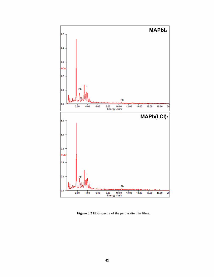
49
Figure 3.2 EDS spectra of the perovskite thin films.
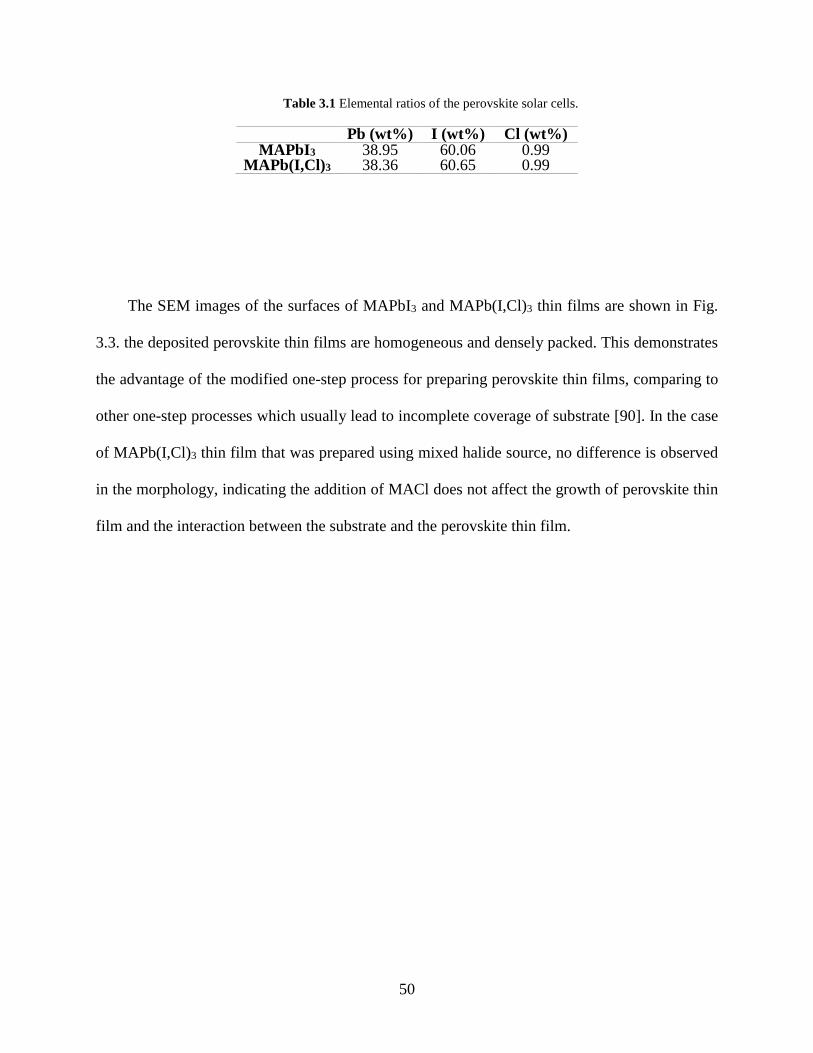
50
Table 3.1 Elemental ratios of the perovskite solar cells.
Pb (wt%) I (wt%) Cl (wt%) MAPbI3 38.95 60.06 0.99
MAPb(I,Cl)3 38.36 60.65 0.99
The SEM images of the surfaces of MAPbI3 and MAPb(I,Cl)3 thin films are shown in Fig.
3.3. the deposited perovskite thin films are homogeneous and densely packed. This demonstrates
the advantage of the modified one-step process for preparing perovskite thin films, comparing to
other one-step processes which usually lead to incomplete coverage of substrate [90]. In the case
of MAPb(I,Cl)3 thin film that was prepared using mixed halide source, no difference is observed
in the morphology, indicating the addition of MACl does not affect the growth of perovskite thin
film and the interaction between the substrate and the perovskite thin film.
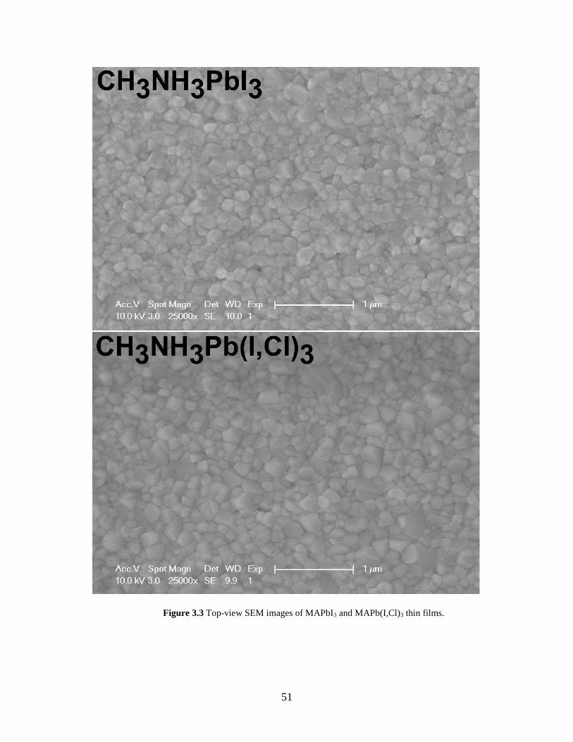
51
Figure 3.3 Top-view SEM images of MAPbI3 and MAPb(I,Cl)3 thin films.
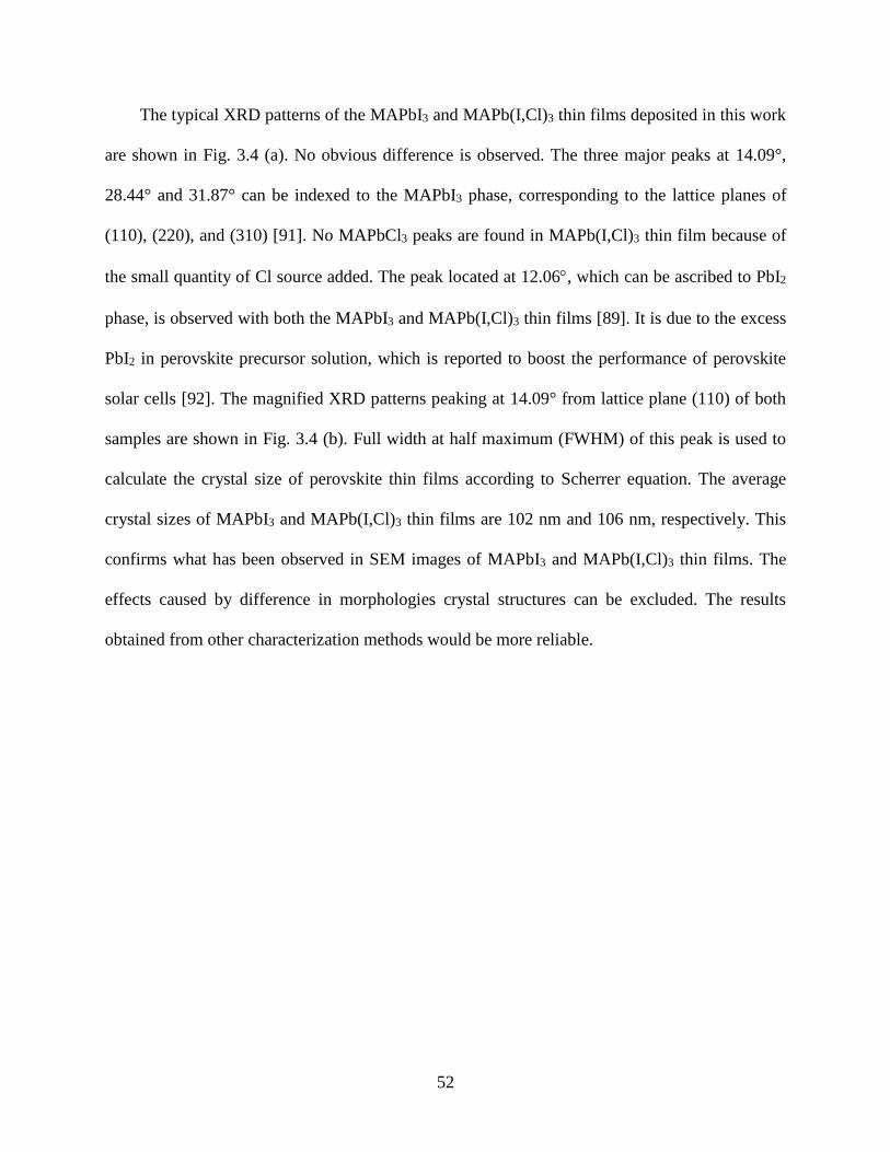
52
The typical XRD patterns of the MAPbI3 and MAPb(I,Cl)3 thin films deposited in this work
are shown in Fig. 3.4 (a). No obvious difference is observed. The three major peaks at 14.09°,
28.44° and 31.87° can be indexed to the MAPbI3 phase, corresponding to the lattice planes of
(110), (220), and (310) [91]. No MAPbCl3 peaks are found in MAPb(I,Cl)3 thin film because of
the small quantity of Cl source added. The peak located at 12.06, which can be ascribed to PbI2
phase, is observed with both the MAPbI3 and MAPb(I,Cl)3 thin films [89]. It is due to the excess
PbI2 in perovskite precursor solution, which is reported to boost the performance of perovskite
solar cells [92]. The magnified XRD patterns peaking at 14.09° from lattice plane (110) of both
samples are shown in Fig. 3.4 (b). Full width at half maximum (FWHM) of this peak is used to
calculate the crystal size of perovskite thin films according to Scherrer equation. The average
crystal sizes of MAPbI3 and MAPb(I,Cl)3 thin films are 102 nm and 106 nm, respectively. This
confirms what has been observed in SEM images of MAPbI3 and MAPb(I,Cl)3 thin films. The
effects caused by difference in morphologies crystal structures can be excluded. The results
obtained from other characterization methods would be more reliable.
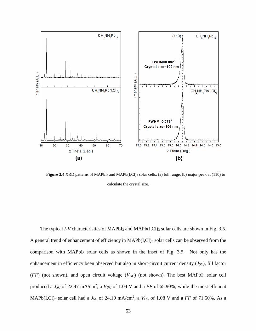
53
Figure 3.4 XRD patterns of MAPbI3 and MAPb(I,Cl)3 solar cells: (a) full range, (b) major peak at (110) to
calculate the crystal size.
The typical I-V characteristics of MAPbI3 and MAPb(I,Cl)3 solar cells are shown in Fig. 3.5.
A general trend of enhancement of efficiency in MAPb(I,Cl)3 solar cells can be observed from the
comparison with MAPbI3 solar cells as shown in the inset of Fig. 3.5. Not only has the
enhancement in efficiency been observed but also in short-circuit current density (JSC), fill factor
(FF) (not shown), and open circuit voltage (VOC) (not shown). The best MAPbI3 solar cell
produced a JSC of 22.47 mA/cm2, a VOC of 1.04 V and a FF of 65.90%, while the most efficient
MAPb(I,Cl)3 solar cell had a JSC of 24.10 mA/cm2, a VOC of 1.08 V and a FF of 71.50%. As a
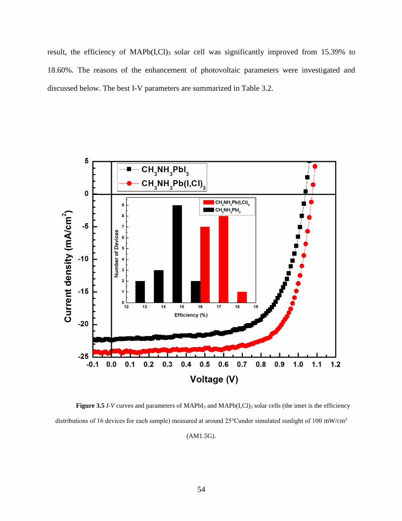
54
result, the efficiency of MAPb(I,Cl)3 solar cell was significantly improved from 15.39% to
18.60%. The reasons of the enhancement of photovoltaic parameters were investigated and
discussed below. The best I-V parameters are summarized in Table 3.2.
Figure 3.5 I-V curves and parameters of MAPbI3 and MAPb(I,Cl)3 solar cells (the inset is the efficiency
distributions of 16 devices for each sample) measured at around 25℃under simulated sunlight of 100 mW/cm2
(AM1.5G).
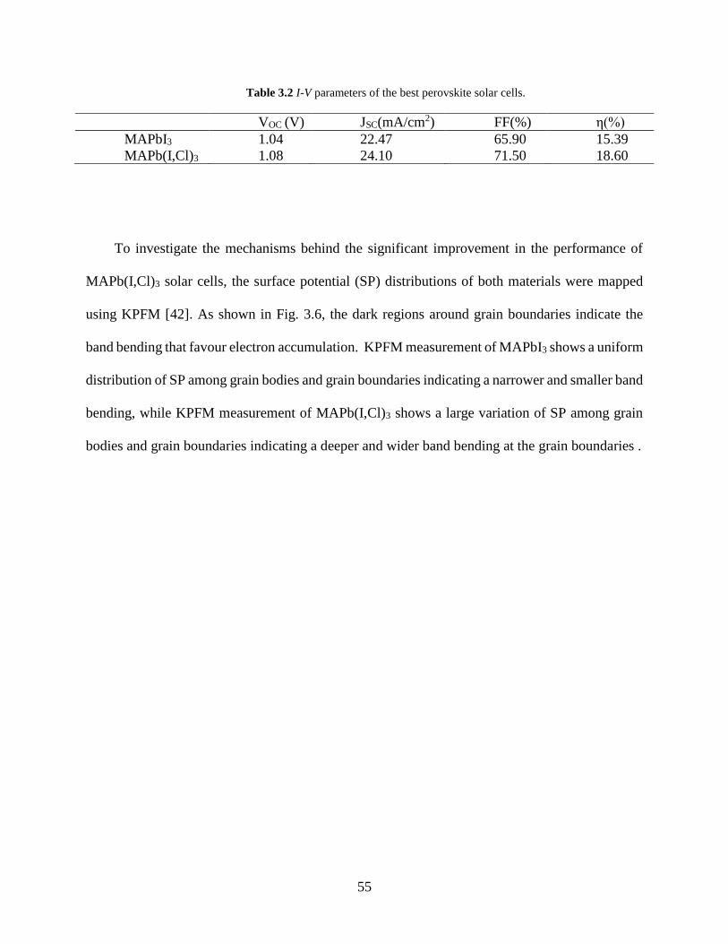
55
Table 3.2 I-V parameters of the best perovskite solar cells.
VOC (V) JSC(mA/cm2) FF(%) η(%)
MAPbI3 1.04 22.47 65.90 15.39
MAPb(I,Cl)3 1.08 24.10 71.50 18.60
To investigate the mechanisms behind the significant improvement in the performance of
MAPb(I,Cl)3 solar cells, the surface potential (SP) distributions of both materials were mapped
using KPFM [42]. As shown in Fig. 3.6, the dark regions around grain boundaries indicate the
band bending that favour electron accumulation. KPFM measurement of MAPbI3 shows a uniform
distribution of SP among grain bodies and grain boundaries indicating a narrower and smaller band
bending, while KPFM measurement of MAPb(I,Cl)3 shows a large variation of SP among grain
bodies and grain boundaries indicating a deeper and wider band bending at the grain boundaries .
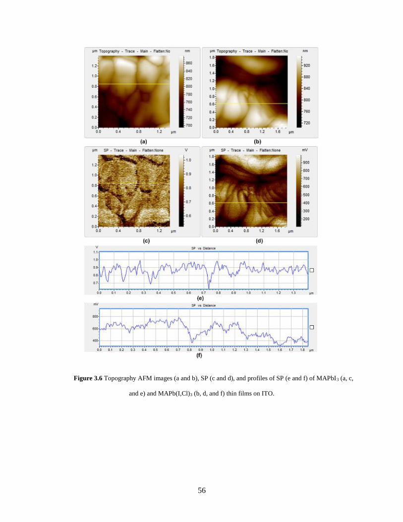
56
Figure 3.6 Topography AFM images (a and b), SP (c and d), and profiles of SP (e and f) of MAPbI3 (a, c,
and e) and MAPb(I,Cl)3 (b, d, and f) thin films on ITO.
57
MAPbI3 was found to be a p-type material [93], thus a single p-n heterojunction should be
formed at the cathode side of the device (Fig. 3.7 (a)). For this single p-n heterojunction, an
electron blocking layer is needed on the anode side. The charge collection efficiency is higher on
the junction side (cathode) but lower on the anode side because only diffusion contributes to the
charger transport on the anode side. The observation of wider and deeper band bending at the
grain boundaries of MAPb(I,Cl)3 from KPFM measurements indicates that electron accumulation
is enhanced at the grain boundaries thus bring the Fermi level closer to the center band to make
MAPb(I,Cl)3 less p-type. Such Fermi level shift results in a p-i-n heterojunction in the device (Fig.
3.7 (b)), first speculated in mesoporous MAPb(I,Cl)3 solar cells [94] and later observed in planar
MAPb(I,Cl)3 solar cells by electron beam-induced current study [95]. The p-i-n heterojunction
facilitates the charge collection on both sides because both drift and diffusion contribute to the
charge transport. In addition, the junction on the anode side provides a blocking barrier to prevent
electrons reaching the anode, thus to reduce recombination loss.
Figure 3.7 Band alignment of devices for (a) MAPbI3 and (b)MAPb(I,Cl)3.
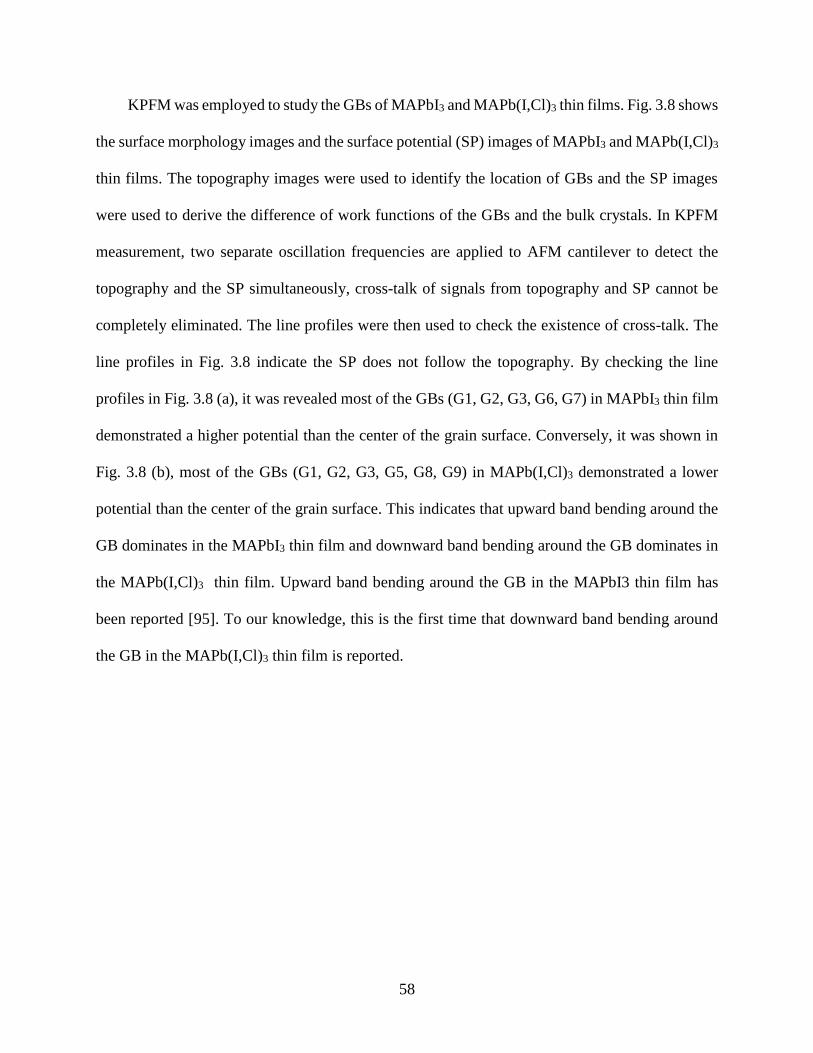
58
KPFM was employed to study the GBs of MAPbI3 and MAPb(I,Cl)3 thin films. Fig. 3.8 shows
the surface morphology images and the surface potential (SP) images of MAPbI3 and MAPb(I,Cl)3
thin films. The topography images were used to identify the location of GBs and the SP images
were used to derive the difference of work functions of the GBs and the bulk crystals. In KPFM
measurement, two separate oscillation frequencies are applied to AFM cantilever to detect the
topography and the SP simultaneously, cross-talk of signals from topography and SP cannot be
completely eliminated. The line profiles were then used to check the existence of cross-talk. The
line profiles in Fig. 3.8 indicate the SP does not follow the topography. By checking the line
profiles in Fig. 3.8 (a), it was revealed most of the GBs (G1, G2, G3, G6, G7) in MAPbI3 thin film
demonstrated a higher potential than the center of the grain surface. Conversely, it was shown in
Fig. 3.8 (b), most of the GBs (G1, G2, G3, G5, G8, G9) in MAPb(I,Cl)3 demonstrated a lower
potential than the center of the grain surface. This indicates that upward band bending around the
GB dominates in the MAPbI3 thin film and downward band bending around the GB dominates in
the MAPb(I,Cl)3 thin film. Upward band bending around the GB in the MAPbI3 thin film has
been reported [95]. To our knowledge, this is the first time that downward band bending around
the GB in the MAPb(I,Cl)3 thin film is reported.
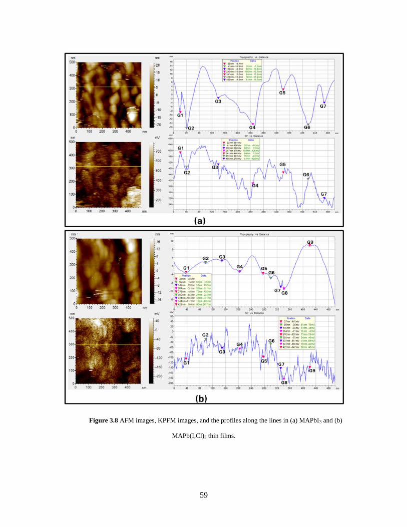
59
Figure 3.8 AFM images, KPFM images, and the profiles along the lines in (a) MAPbI3 and (b)
MAPb(I,Cl)3 thin films.
60
The band diagrams around the GB in MAPbI3 and MAPb(I,Cl)3 thin films are plotted in Fig.
3.9 with an assumption that the GB and the grain have same bandgap values. It has been reported
MAPbI3 thin film shows p-type conductivity [96]. The incorporation of a small amount of Cl atoms
into MAPbI3 thin film does not likely reverse the conductivity type because Cl and I belong to the
same halogen group. Therefore, the transport behavior of electrons (minority carriers) in MAPbI3
and MAPb(I,Cl)3 thin films significantly affects the performance of perovskite solar cells. The
potential barrier due to the upward band bending at GB in MAPbI3 thin film repels electrons and
attracts holes. The electrons will have to be transported to the cathode through the grain bulk where
majority holes (majority carriers) have a high concentration, resulting in higher recombination
rate. On the contrary, the potential barrier due to the downward band bending at GB in
MAPb(I,Cl)3 thin film repels holes and attracts electrons. The electrons will be transported to the
cathode through both the grain bulk and GB where majority holes (majority carriers) are depleted,
resulting in a higher collection area and a lower recombination rate. This will again benefit the
diffusion length and the performance of solar cells such as VOC and FF. Considering the low
concentration of Cl allowed to be incorporated into MAPbI3 thin film, the properties of bulk grains
should not change significantly. As observed in the KPFM measurement, the properties of the GBs
in MAPbI3 thin film have been significantly affected, which could be attributed to the
accumulation of Cl atoms in the GBs as sodium atoms do in CIGS thin films[97]. This would be
verified by high definition element mapping technique such as TEM, which is ongoing in our
research.
61
Figure 3.9 Band diagrams around the GB in MAPbI3 and MAPb(I,Cl)3 thin films.
The measurement of electron lifetime can be applied to quantify the extent of electron
recombination in perovskite solar cells [33]. The dependence of electron lifetime on the VOC for
planar perovskite solar cells fabricated with single and mixed halide source is shown in Fig. 3.10.
It clearly demonstrates that the electron lifetime of the MAPb(I,Cl)3 solar cells is longer than that
of the MAPbI3 solar cell. This suggests that the electrons in MAPb(I,Cl)3 thin film can survive
longer and demonstrate a longer diffusion length as reported in literatures [98, 99].
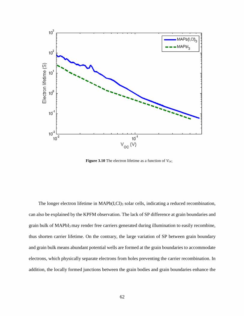
62
Figure 3.10 The electron lifetime as a function of VOC.
The longer electron lifetime in MAPb(I,Cl)3 solar cells, indicating a reduced recombination,
can also be explained by the KPFM observation. The lack of SP difference at grain boundaries and
grain bulk of MAPbI3 may render free carriers generated during illumination to easily recombine,
thus shorten carrier lifetime. On the contrary, the large variation of SP between grain boundary
and grain bulk means abundant potential wells are formed at the grain boundaries to accommodate
electrons, which physically separate electrons from holes preventing the carrier recombination. In
addition, the locally formed junctions between the grain bodies and grain boundaries enhance the
63
dissociation of excitons and further suppress recombination. As a result, carrier life time is greatly
improved in MAPb(I,Cl)3 solar cells.
The AS technique has been well established to investigate the defect levels of thin film
solar cells such as CIGS and CdTe [100-102]. It has been rarely applied to perovskite solar cells.
So far, only two groups have addressed the defect density of MAPbI3 solar cells using AS
technique. In 2014, Dalal et al. found two defect levels in MAPbI3 solar cell. One is 0.24 eV and
the other is 0.65 eV above the valence band with a peak density value of 3×10¹⁶/(cm3·eV) [103].
In the same year, Yang et al. revealed a deep defect state of 0.17 eV above the valence band with
a peak density value of 2×10¹⁷/(cm3·eV) [104]. The cause of the difference in defect levels and
densities is not clear. They might be attributed to the difference in MAPbI3 thin films because the
deposition method for MAPbI3 thin film used by one group is different from the method used by
the other group. To investigate the mechanisms behind the significant improvement in the
MAPb(I,Cl)3 solar cell, we applied the AS method to MAPbI3 and MAPb(I,Cl)3 solar cells
fabricated by the exactly same procedures. As discussed earlier, the resultant MAPbI3 and
MAPb(I,Cl)3 thin films were highly similar in morphology and crystal structure. The results
obtained from AS method, as shown in Fig. 3.11, should be more reliable to reveal the origin of
the significant performance improvement observed in MAPb(I,Cl)3 solar cells. The defect levels
of MAPbI3 and MAPb(I,Cl)3 solar cells derived from Arrhenius plot, as shown in Fig. 3.11 (a), are
0.214 eV and 0.208 eV, respectively. The difference of 6 meV could come from the measurement
error. The energy distributions of the defects are shown in Fig. 3.11 (b). For MAPbI3 solar cell,
the defect density peaks at 7.2×10¹⁷/(cm3·eV), while the peak defect density of MAPb(I,Cl)3 solar
cell is reduced to 3.8×10¹⁷/(cm3·eV). The spans of defect states can be fitted as a Gaussian
distribution (the solid lines). The integrated defect density of MAPbI3 solar cell is 4.68×1016 cm-3
64
and that of MAPb(I,Cl)3 solar cell is reduced to 2.34×1016 cm-3. A reduced defect density has been
experimentally observed in MAPb(I,Cl)3 solar cells. The result is in good agreement with what has
been proposed in the electron lifetime measurement: Cl helps to passivate the defects in
MAPb(I,Cl)3 solar cells, leading to a lower defect density and higher electron lifetime. Thus,
OCVD and AS jointly demonstrate that Cl plays an extremely important role in suppressing the
defect in perovskite devices. Further investigation is required and under way to understand the
origin of this defect and why Cl is able to suppress the formation of defect when depositing
perovskite thin films.
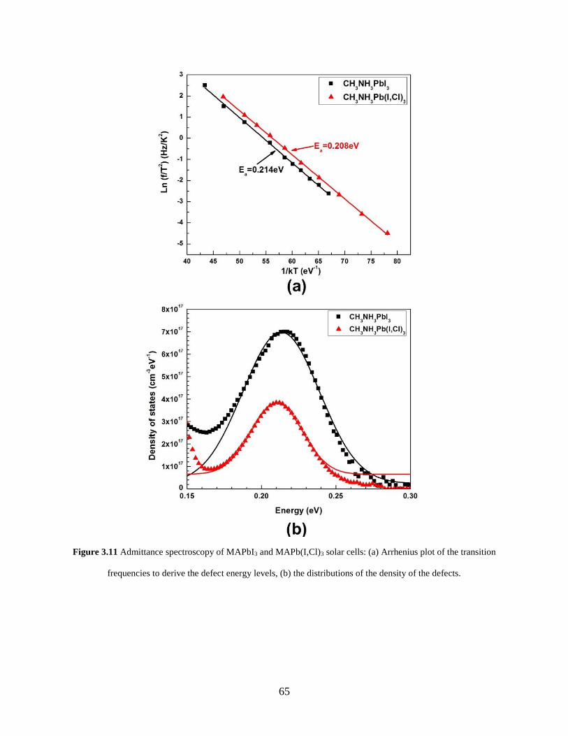
65
Figure 3.11 Admittance spectroscopy of MAPbI3 and MAPb(I,Cl)3 solar cells: (a) Arrhenius plot of the transition
frequencies to derive the defect energy levels, (b) the distributions of the density of the defects.
66
CHLORINE-ASSISTED RECOVERY OF PERFORMANCE LOSS IN MAPBI3
PEROVSKITE SOLAR CELL MADE FROM LOW PURITY PBI2
High purity (9~11N) silicon has been required to manufacture integrated circuits and was
traditionally used to fabricate photovoltaic (PV) devices [105, 106]. Due to the nature of low
density of sunlight, large area of PV devices is needed to generate applicable electricity [107]. The
high cost and shortage of high purity silicon, however, limit the deployment of PV devices.
Comparatively low purity silicon such as solar-grade (5~6N) silicon has been developed and
currently widely used in the PV industry [108]. Nevertheless, the impurities in low purity silicon
are known to reduce minority carrier diffusion length in silicon-based PV devices [109, 110],
leading to degraded solar-to-electricity conversion efficiency [111-113]. Several methods, such as
external and internal gettering, have been approved to be capable of improving the quality of low
purity silicon, especially for minority carrier lifetime [105, 114, 115].
Organic-inorganic hybrid perovskite solar cell has recently become an intensively explored
topic in PV field because of its high performance and potentially low manufacturing cost.
Significant efforts have been focused on developing high quality perovskite thin films and
improving the stability of perovskite solar cells. To this date, lead sources such PbI2 and PbCl2
with a purity of 99.999% (5N), have been widely in fabricating highly efficient perovskite solar
cells [116], which is the major concern regarding the mass deployment of perovskite solar cells,
not to mention the high cost and the adverse impact on the environment associated with the
67
purifying process [117]. Recently, the purity of raw materials, which is known to significantly
affect the performance of both organic [118] and inorganic [119] solar cells, as well as silicon-
based solar cells, has been investigated for perovskite solar cells [120]. It was found that perovskite
solar cells using highly pure (5N) PbI2 showed an efficiency of 16.4%, which was higher than that
of perovskite solar cells with low purity (2N) PbI2 by 30–40%, indicating highly pure PbI2 is
indispensable for highly efficient perovskite solar cells.
4.1 EXPERIMENTAL PROCEDURES
4.1.1 Fabrication of MAPbI3 Solar Cells using PbI2 with different purtities
Planar perovskite solar cells were fabricated in air with a structure of FTO/TiO2/perovskite/spiro-
MeOTAD/Au. A modified one-step process capable of incorporating Cl is used to grow the
perovskite thin films [89]. PbI2 with different purities (99% and 99.999%) were purchased from
Sigma Aldrich and were used without further processing. The experimental procedures described
in 3.1.2 were employed to deposit MAPbI3 thin films and fabricate MAPbI3 solar cells.
4.2 RESULTS AND ANALYSIS
In this work, the effects of Cl on perovskite solar cells fabricated using high and low purity PbI2
were investigated. The averaged I–V curves of these devices fabricated using the same
experimental procedures are shown in Fig. 4.1. As shown in the inserted table in Fig. 4.1, the
68
averaged performance parameters, including VOC, JSC, FF, and efficiency (Eff.), are significantly
affected by the purity of PbI2. The perovskite solar cell with high purity PbI2 exhibited a high
efficiency of 16.39 % with a JSC of 23.46 mA/cm2, VOC of 1.07 V, and FF of 65.31%, while that
with low purity PbI2 had a comparatively low efficiency of 14.16% with a JSC of 21.94 mA/cm2,
VOC of 1.04 V, and FF of 62.07 %. This agrees well with what has been reported in literature [120].
Excitingly, the efficiency of perovskite solar cell with low purity PbI2 was significantly boosted to
16.58% after a small amount of Cl source was added. The lost efficiency in low purity perovskite
solar cells is fully recovered when Cl is added. The resulted efficiency is even slightly higher than
that obtained from high purity perovskite solar cells. This indicates that, besides the costly way of
increasing the purity of raw materials, Cl doping could provide a cost-effective way to further
improve the performance of perovskite solar cells.
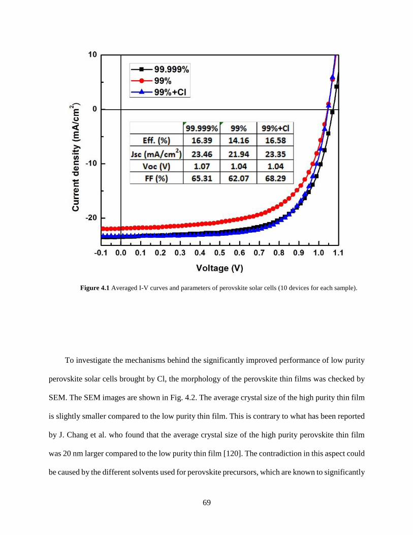
69
Figure 4.1 Averaged I-V curves and parameters of perovskite solar cells (10 devices for each sample).
To investigate the mechanisms behind the significantly improved performance of low purity
perovskite solar cells brought by Cl, the morphology of the perovskite thin films was checked by
SEM. The SEM images are shown in Fig. 4.2. The average crystal size of the high purity thin film
is slightly smaller compared to the low purity thin film. This is contrary to what has been reported
by J. Chang et al. who found that the average crystal size of the high purity perovskite thin film
was 20 nm larger compared to the low purity thin film [120]. The contradiction in this aspect could
be caused by the different solvents used for perovskite precursors, which are known to significantly
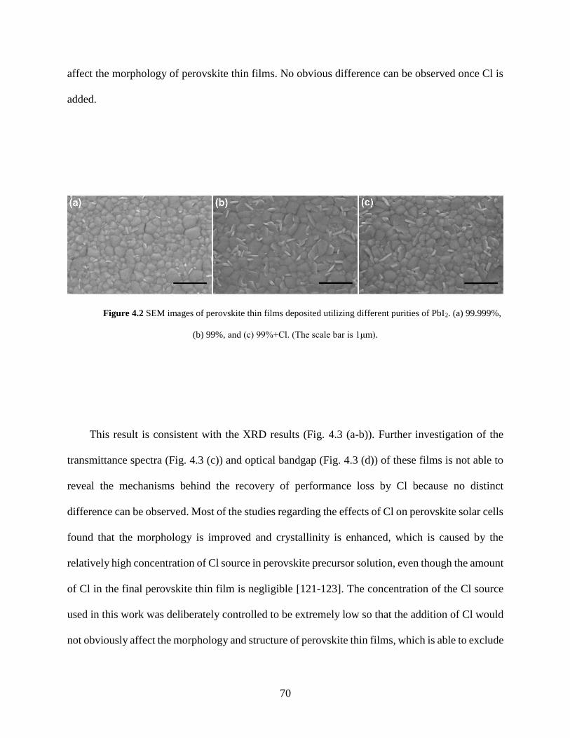
70
affect the morphology of perovskite thin films. No obvious difference can be observed once Cl is
added.
Figure 4.2 SEM images of perovskite thin films deposited utilizing different purities of PbI2. (a) 99.999%,
(b) 99%, and (c) 99%+Cl. (The scale bar is 1μm).
This result is consistent with the XRD results (Fig. 4.3 (a-b)). Further investigation of the
transmittance spectra (Fig. 4.3 (c)) and optical bandgap (Fig. 4.3 (d)) of these films is not able to
reveal the mechanisms behind the recovery of performance loss by Cl because no distinct
difference can be observed. Most of the studies regarding the effects of Cl on perovskite solar cells
found that the morphology is improved and crystallinity is enhanced, which is caused by the
relatively high concentration of Cl source in perovskite precursor solution, even though the amount
of Cl in the final perovskite thin film is negligible [121-123]. The concentration of the Cl source
used in this work was deliberately controlled to be extremely low so that the addition of Cl would
not obviously affect the morphology and structure of perovskite thin films, which is able to exclude

71
the effects of morphology and structure when investigating the mechanisms behind the Cl-assisted
recovery of performance loss in low purity MAPbI3 solar cells.
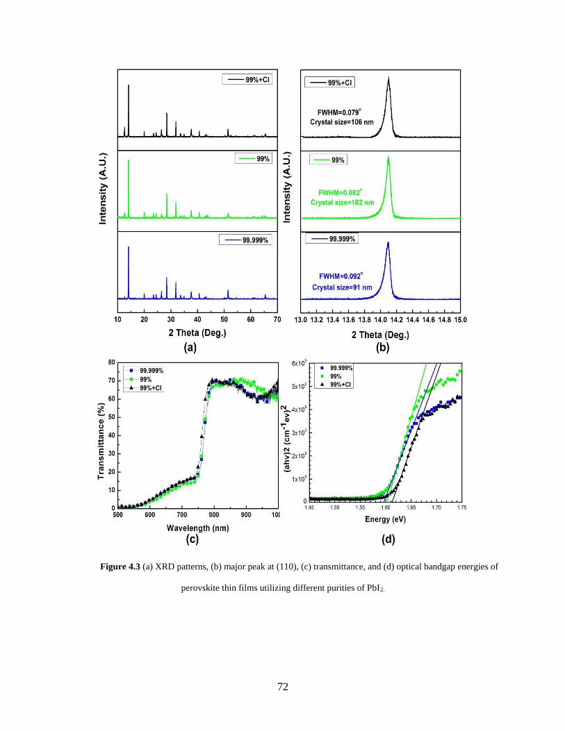
72
Figure 4.3 (a) XRD patterns, (b) major peak at (110), (c) transmittance, and (d) optical bandgap energies of
perovskite thin films utilizing different purities of PbI2.
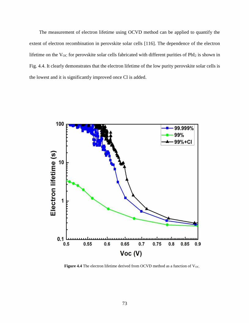
73
The measurement of electron lifetime using OCVD method can be applied to quantify the
extent of electron recombination in perovskite solar cells [116]. The dependence of the electron
lifetime on the VOC for perovskite solar cells fabricated with different purities of PbI2 is shown in
Fig. 4.4. It clearly demonstrates that the electron lifetime of the low purity perovskite solar cells is
the lowest and it is significantly improved once Cl is added.
Figure 4.4 The electron lifetime derived from OCVD method as a function of VOC.
74
It is well known that low purity absorber materials in solar cells usually demonstrate high
defect density caused by the high impurity concentration, leading to a decreased carrier lifetime,
and therefore reduced conversion efficiency [124-127]. Admittance spectroscopy (AS) is widely
applied to derive the distribution of defect density and the energy levels of the defects in the
bandgap by measuring the capacitance of the solar cell at different temperatures [103, 128, 129].
Fig. 4.5 (a) shows the capacitance spectra of perovskite solar cell fabricated using low purity PbI2
with Cl (99%+Cl) obtained at different temperatures (T=150 K to 296 K) in the dark with the
frequency ranging from 102 to 106 Hz. Steps are observed in each capacitance spectrum at different
temperatures. The transition frequency, where the capacitance step lies, can be found by taking the
derivative of the capacitance spectra as shown in Fig. 4.5 (b). The energy levels of the defects can
be obtained by linearly fitting the Arrhenius plot of the transition frequencies as illustrated in Fig.
4.5 (c). The energy level of the defect in perovskite solar cell fabricated using low purity PbI2 with
Cl is fitted to be 208.48 meV above the valence band, which is close to the energy levels of the
defects in other samples (Fig. 4.6). The defect levels revealed in this work are different from the
defect level of 167 meV found by Duan et al., which can be ascribed to the iodine interstitials [104,
130]. Samiee et al. found a defect level of 240 meV [103]. The origin of these two defects is not
clear, which could be the impurities of the raw materials of perovskite thin films. The defect
densities as a function of energy at different temperatures can be deduced from the differentiated
capacitance spectra as shown in Fig. 4.5 (d).
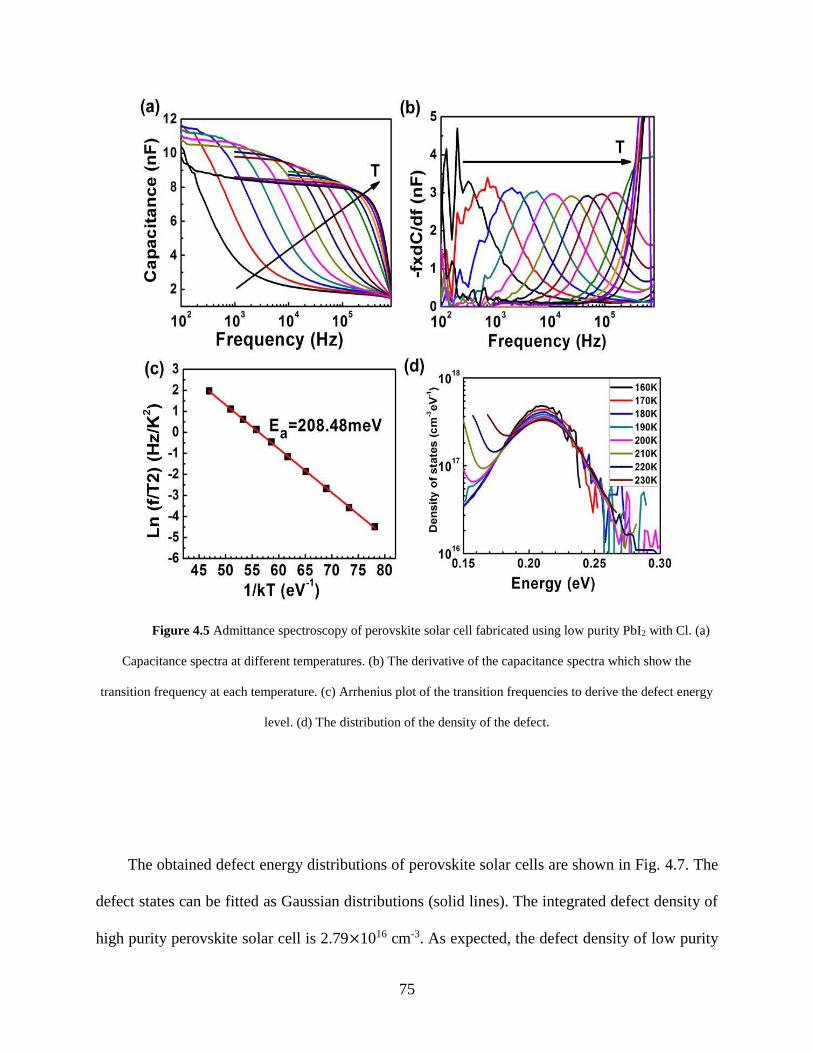
75
Figure 4.5 Admittance spectroscopy of perovskite solar cell fabricated using low purity PbI2 with Cl. (a)
Capacitance spectra at different temperatures. (b) The derivative of the capacitance spectra which show the
transition frequency at each temperature. (c) Arrhenius plot of the transition frequencies to derive the defect energy
level. (d) The distribution of the density of the defect.
The obtained defect energy distributions of perovskite solar cells are shown in Fig. 4.7. The
defect states can be fitted as Gaussian distributions (solid lines). The integrated defect density of
high purity perovskite solar cell is 2.79×1016 cm-3. As expected, the defect density of low purity
76
sample is higher (4.68×1016 cm-3). Surprisingly, the defect density is reduced to 2.34×1016 cm-3
once Cl is added to low purity sample. Besides the effects of Cl on morphology and crystal
structure as mentioned above, another reported effect is the longer carrier lifetime in Cl-
incorporated perovskite thin film revealed by photoluminescence (PL) spectroscopy [121, 131]. It
is often assumed that this longer carrier lifetime is attributed to reduced defect density [132], which
has never been experimentally approved for perovskite solar cells. This is the first time that
reduced defect density is experimentally observed in Cl-incorporated perovskite solar cells. The
result is in good agreement with what has been observed in the electron lifetime measurement: Cl
helps to passivate the defects in low purity perovskite solar cells, leading to a lower defect density
and higher electron lifetime.
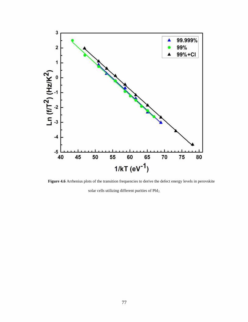
77
Figure 4.6 Arrhenius plots of the transition frequencies to derive the defect energy levels in perovskite
solar cells utilizing different purities of PbI2.
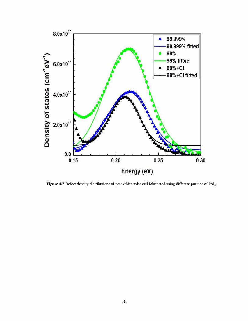
78
Figure 4.7 Defect density distributions of perovskite solar cell fabricated using different purities of PbI2.
79
IMPROVED STABILITY OF MAPBI3 SOLAR CELLS USING ALL INORGANIC
CHARGE TRANSPORT LAYERS (CTLS)
Methylammonium lead halide perovskites (abbreviated as perovskite) have been proved as
promising photovoltaic (PV) materials due to their excellent photoelectric properties [93].
Moreover, the abundant raw materials and the solution process capability make perovskite suitable
for low cost PV technologies similarly as Cu(In,Ga)(S,Se)2 (CIGS) and Cu2ZnSn(S,Se)4 (CZTS)
for low cost PV technologies [57, 59, 87, 133]. The efficiency of perovskite solar cells has been
rapidly improved from 3.8 % in 2009 [12] to 20.1% in 2015 [1]. This great advancement is mainly
attributed to the numerous efforts that have been taken to deposit high quality perovskite thin films
by many research groups [17-19]. The tremendous improvement can also be attributed to the two
photovoltaic (PV) device structures developed for almost 20 years. One structure is based on TiO2
as an electron transport layer (ETL) and 2,20,7,70-tetrakis(N,N-di-4-methoxyphenylamino)-9,90-
spirobifluorene (spiro-OMeTAD) as a hole transport layer (HTL). The other structure is based on
the organic ETL such as PCBM and organic HTL such as poly(3,4-ethylenedioxythiophene)
polystyrene sulfonate (PEDOT:PSS) and poly(3-hexylthiophene-2,5-diyl) (P3HT). The perovskite
thin film is deposited as an absorber layer to fabricate perovskite solar cells. Due to the high
sensitivity of these organic materials to moisture and oxygen, a nitrogen glove box with a strict
control of the moisture and oxygen levels was usually used to fabricate perovskite solar cells [17,
80
22-25]. However, the perovskite solar cells degrade rapidly once they are removed from the
nitrogen glove box and stored in ambient environment [26-28].
It was reported that perovskite thin films were comparatively stable in ambient
environment with low humidity [134]. The rapid degradation of perovskite solar cells was mainly
caused by the instability of the organic charge transport layers (CTLs) [135, 136]. Encapsulation
of perovskite solar cells was reported to be able to improve the stability of perovskite solar cells
[137]. However, encapsulation is usually a final process step for fabrication of perovskite solar
cells. The perovskite solar cell could have already degraded before being encapsulated. Another
reported approach to improve the stability of perovskite solar cells was to use NiOx thin film as
HTL to replace those organic ones [138, 139]. Nevertheless, the remained organic ETL such as
PCBM still significantly affect the stability of perovskite solar cells [135, 136]. The ultimate
advancement in the device stability of perovskite solar cells has yet to be realized.
Here, solution-processed inorganic thin films, lithium (Li)-doped NiOx (Li:NiOx) and ZnO
nanoparticles (NPs), were deposited as the HTL and ETL, respectively, to fabricate highly stable,
highly performed planar perovskite solar cells. The devices were intentionally kept and tested in
ambient environment without encapsulation to focus on the efficiency and stability. The
employment of all inorganic thin films as CTLs has significantly improved the stability of
perovskite solar cells compared to that of conventional perovskite solar cell structure with TiO2 as
the ETL and spiro-MeOTAD as the HTL. This study provides an excellent device structure for
making highly stable and efficient perovskite solar cells.
81
5.1 EXPERIMENTAL PROCEDURES
5.1.1 Synthesis of ZnO Nanoparticles (NPs)
ZnO NPs were synthesized according to a reported procedure [140]. Zinc acetate dihydrate
(molecular weight: 219.51) (2.95 g, 13.4 mmol) was dissolved in 125 ml methanol with stirring at
65 ℃. A solution of potassium hydroxide (molecular weight: 56.11) (1.48 g, 23 mmol) in 65 ml
methanol was then added dropwise over a period of 15 min to the zinc acetate dehydrate solution.
The reaction mixture was stirred for 2.5h at 65 ℃ . After cooling to room temperature, the
supernatant was decanted and the precipitate was washed twice with methanol (20 ml). n-butanol
(70 ml), methanol (5 ml) and chloroform (5 ml) were added to disperse the precipitate and produce
a ZnO NPs solution with a concentration of 6 mg/ml. Before use, the ZnO NPs solution was filtered
through a 0.45 µm PVDF syringe filter.
5.1.2 Preparation of Li-doped NiOx (Li:NiOx) sol-gel
Li:NiOx sol-gel solution was prepared according to a reported procedure [141]. Nickel acetate
tetrahydrate (Ni(COOCH3)2·4H2O, 746.52mg) was dissolved in 2-methoxyethanol (2ME) (10 ml),
and 0.1 ml hydrochloric acid (HCl) was added as catalyst. Lithium acetate monohydrate
(LiCH3COO·H2O, 29.94 mg) was used as the dopant. The solution was stirred in water bath at 60
℃for 1 h and then aged for 24 h at room temperature.
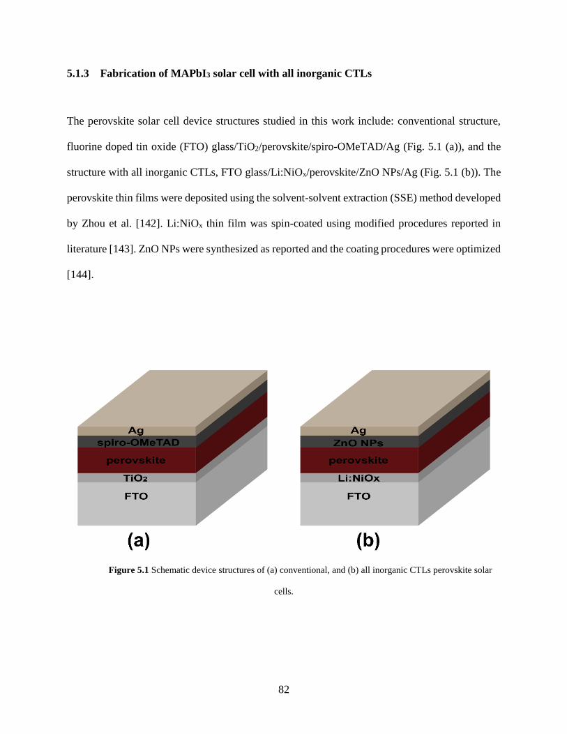
82
5.1.3 Fabrication of MAPbI3 solar cell with all inorganic CTLs
The perovskite solar cell device structures studied in this work include: conventional structure,
fluorine doped tin oxide (FTO) glass/TiO2/perovskite/spiro-OMeTAD/Ag (Fig. 5.1 (a)), and the
structure with all inorganic CTLs, FTO glass/Li:NiOx/perovskite/ZnO NPs/Ag (Fig. 5.1 (b)). The
perovskite thin films were deposited using the solvent-solvent extraction (SSE) method developed
by Zhou et al. [142]. Li:NiOx thin film was spin-coated using modified procedures reported in
literature [143]. ZnO NPs were synthesized as reported and the coating procedures were optimized
[144].
Figure 5.1 Schematic device structures of (a) conventional, and (b) all inorganic CTLs perovskite solar
cells.
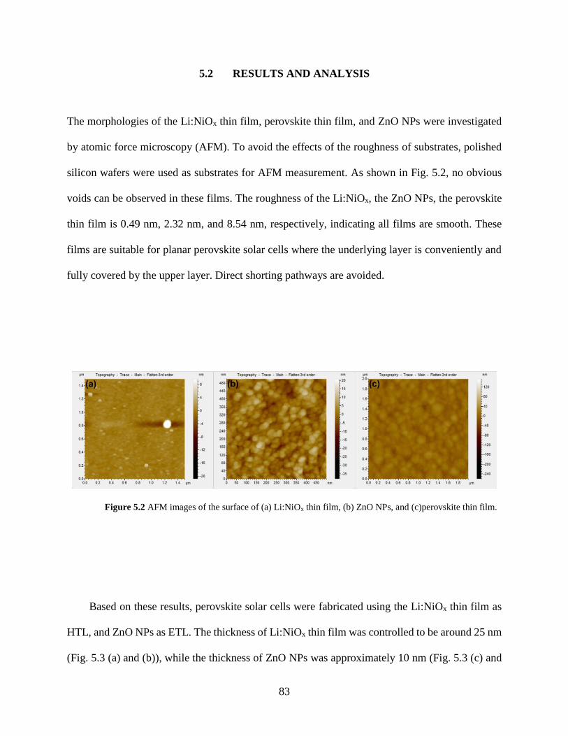
83
5.2 RESULTS AND ANALYSIS
The morphologies of the Li:NiOx thin film, perovskite thin film, and ZnO NPs were investigated
by atomic force microscopy (AFM). To avoid the effects of the roughness of substrates, polished
silicon wafers were used as substrates for AFM measurement. As shown in Fig. 5.2, no obvious
voids can be observed in these films. The roughness of the Li:NiOx, the ZnO NPs, the perovskite
thin film is 0.49 nm, 2.32 nm, and 8.54 nm, respectively, indicating all films are smooth. These
films are suitable for planar perovskite solar cells where the underlying layer is conveniently and
fully covered by the upper layer. Direct shorting pathways are avoided.
Figure 5.2 AFM images of the surface of (a) Li:NiOx thin film, (b) ZnO NPs, and (c)perovskite thin film.
Based on these results, perovskite solar cells were fabricated using the Li:NiOx thin film as
HTL, and ZnO NPs as ETL. The thickness of Li:NiOx thin film was controlled to be around 25 nm
(Fig. 5.3 (a) and (b)), while the thickness of ZnO NPs was approximately 10 nm (Fig. 5.3 (c) and
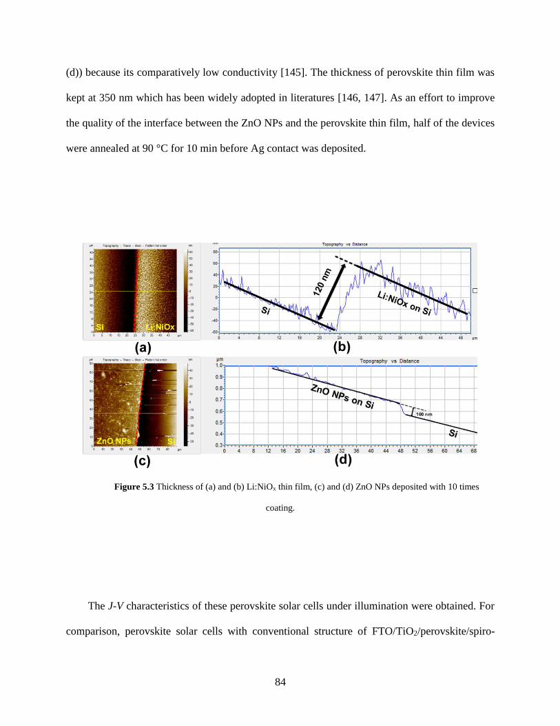
84
(d)) because its comparatively low conductivity [145]. The thickness of perovskite thin film was
kept at 350 nm which has been widely adopted in literatures [146, 147]. As an effort to improve
the quality of the interface between the ZnO NPs and the perovskite thin film, half of the devices
were annealed at 90 °C for 10 min before Ag contact was deposited.
Figure 5.3 Thickness of (a) and (b) Li:NiOx thin film, (c) and (d) ZnO NPs deposited with 10 times
coating.
The J-V characteristics of these perovskite solar cells under illumination were obtained. For
comparison, perovskite solar cells with conventional structure of FTO/TiO2/perovskite/spiro-
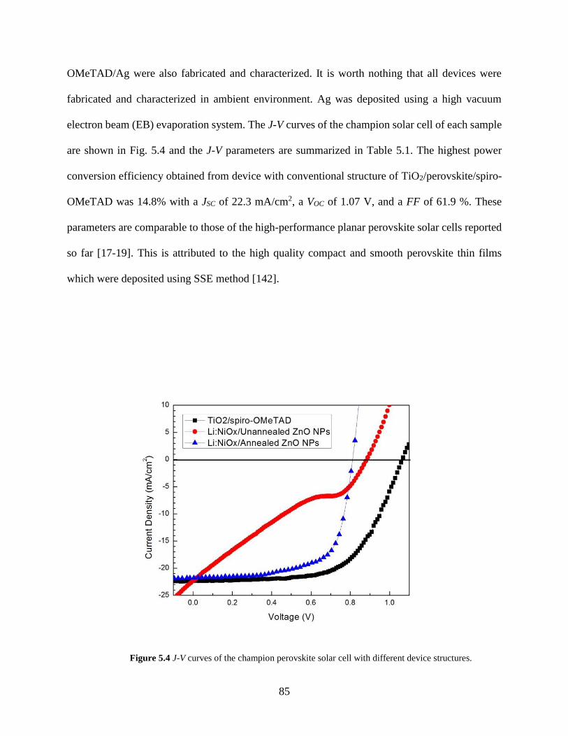
85
OMeTAD/Ag were also fabricated and characterized. It is worth nothing that all devices were
fabricated and characterized in ambient environment. Ag was deposited using a high vacuum
electron beam (EB) evaporation system. The J-V curves of the champion solar cell of each sample
are shown in Fig. 5.4 and the J-V parameters are summarized in Table 5.1. The highest power
conversion efficiency obtained from device with conventional structure of TiO2/perovskite/spiro-
OMeTAD was 14.8% with a JSC of 22.3 mA/cm2, a VOC of 1.07 V, and a FF of 61.9 %. These
parameters are comparable to those of the high-performance planar perovskite solar cells reported
so far [17-19]. This is attributed to the high quality compact and smooth perovskite thin films
which were deposited using SSE method [142].
Figure 5.4 J-V curves of the champion perovskite solar cell with different device structures.
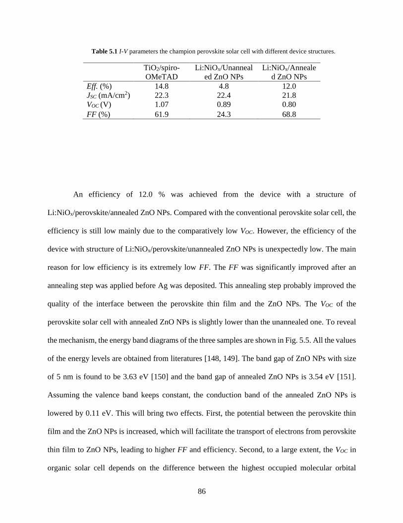
86
Table 5.1 I-V parameters the champion perovskite solar cell with different device structures.
TiO2/spiro-
OMeTAD
Li:NiOx/Unanneal
ed ZnO NPs
Li:NiOx/Anneale
d ZnO NPs
Eff. (%) 14.8 4.8 12.0
JSC (mA/cm2) 22.3 22.4 21.8
VOC (V) 1.07 0.89 0.80
FF (%) 61.9 24.3 68.8
An efficiency of 12.0 % was achieved from the device with a structure of
Li:NiOx/perovskite/annealed ZnO NPs. Compared with the conventional perovskite solar cell, the
efficiency is still low mainly due to the comparatively low VOC. However, the efficiency of the
device with structure of Li:NiOx/perovskite/unannealed ZnO NPs is unexpectedly low. The main
reason for low efficiency is its extremely low FF. The FF was significantly improved after an
annealing step was applied before Ag was deposited. This annealing step probably improved the
quality of the interface between the perovskite thin film and the ZnO NPs. The VOC of the
perovskite solar cell with annealed ZnO NPs is slightly lower than the unannealed one. To reveal
the mechanism, the energy band diagrams of the three samples are shown in Fig. 5.5. All the values
of the energy levels are obtained from literatures [148, 149]. The band gap of ZnO NPs with size
of 5 nm is found to be 3.63 eV [150] and the band gap of annealed ZnO NPs is 3.54 eV [151].
Assuming the valence band keeps constant, the conduction band of the annealed ZnO NPs is
lowered by 0.11 eV. This will bring two effects. First, the potential between the perovskite thin
film and the ZnO NPs is increased, which will facilitate the transport of electrons from perovskite
thin film to ZnO NPs, leading to higher FF and efficiency. Second, to a large extent, the VOC in
organic solar cell depends on the difference between the highest occupied molecular orbital
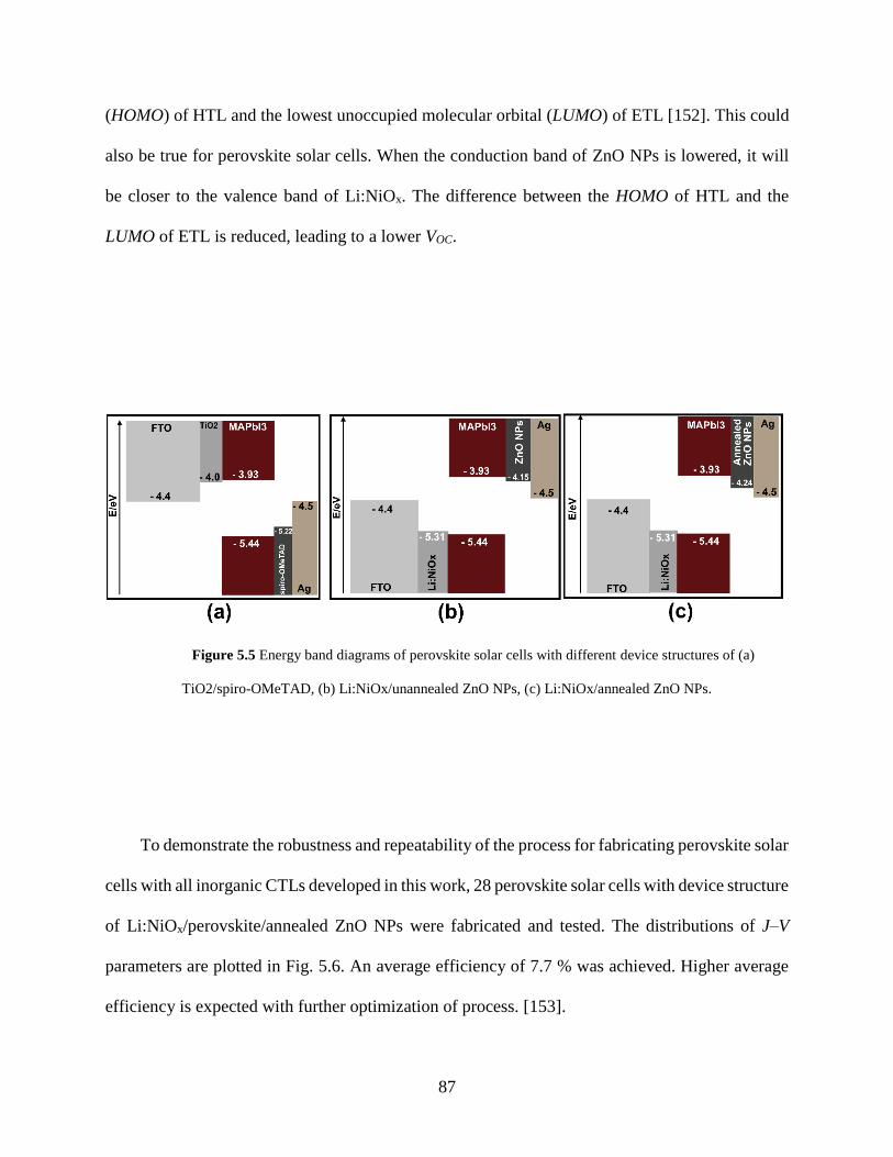
87
(HOMO) of HTL and the lowest unoccupied molecular orbital (LUMO) of ETL [152]. This could
also be true for perovskite solar cells. When the conduction band of ZnO NPs is lowered, it will
be closer to the valence band of Li:NiOx. The difference between the HOMO of HTL and the
LUMO of ETL is reduced, leading to a lower VOC.
Figure 5.5 Energy band diagrams of perovskite solar cells with different device structures of (a)
TiO2/spiro-OMeTAD, (b) Li:NiOx/unannealed ZnO NPs, (c) Li:NiOx/annealed ZnO NPs.
To demonstrate the robustness and repeatability of the process for fabricating perovskite solar
cells with all inorganic CTLs developed in this work, 28 perovskite solar cells with device structure
of Li:NiOx/perovskite/annealed ZnO NPs were fabricated and tested. The distributions of J–V
parameters are plotted in Fig. 5.6. An average efficiency of 7.7 % was achieved. Higher average
efficiency is expected with further optimization of process. [153].
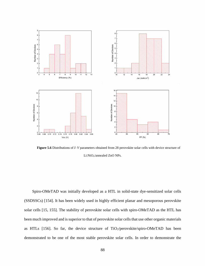
88
Figure 5.6 Distributions of I–V parameters obtained from 28 perovskite solar cells with device structure of
Li:NiOx/annealed ZnO NPs.
Spiro-OMeTAD was initially developed as a HTL in solid-state dye-sensitized solar cells
(SSDSSCs) [154]. It has been widely used in highly efficient planar and mesoporous perovskite
solar cells [15, 155]. The stability of perovskite solar cells with spiro-OMeTAD as the HTL has
been much improved and is superior to that of perovskite solar cells that use other organic materials
as HTLs [156]. So far, the device structure of TiO2/perovskite/spiro-OMeTAD has been
demonstrated to be one of the most stable perovskite solar cells. In order to demonstrate the
89
advantages of the all inorganic CTL perovskite solar cells developed in this work, the perovskite
solar cells with the conventional device structure of TiO2/perovskite/spiro-OMeTAD and the
device structure of Li:NiOx/perovskite/ZnO NP were stored without encapsulation and tested in
ambient environment at 22 ℃ with a relative humidity of 48.5 %. Fig. 5.7 shows the evolution of
J-V parameters for typical devices from each device structure, which were stored in dark for 300
h. For each device structure, the J-V parameters were obtained from 8 solar cells with efficiencies
ranging from 10 % to 5%. As shown in Fig. 4.32 (a), the efficiency of Li:NiOx/ZnO NP structure
was preserved 95 % of the initial performance, while the efficiency of TiO2/spiro-OMeTAD
structure rapidly decreased to 33 % after 100 h storage in dark. Remarkably, the JSC of the
Li:NiOx/ZnO NP device improved during the first 50 h, while the VOC and FF relatively
unchanged. For devices with the TiO2/spiro-OMeTAD structure, the JSC and VOC decreased
rapidly, while the FF fluctuated. Unexpectedly, the efficiency of TiO2/spiro-OMeTAD device was
degraded to less than 1 % of its initial efficiency after 170 h. This was mainly caused by the severe
degradation of VOC which only preserved 3 % of its initial value. At this point, the efficiency of
Li:NiOx/ZnO NP device preserved 92 % mainly caused by the slight degradation of JSC. The
stability test of Li:NiOx/ZnO NP device was continued to 300 h, while that of TiO2/spiro-
OMeTAD device was stopped at 170 h. At the end of the test, the values of VOC and FF were
comparable to their initial values. The JSC slowly degraded to 62 %. As a result, the efficiency of
Li:NiOx/ZnO NP device was preserved 61 % of the initial value.
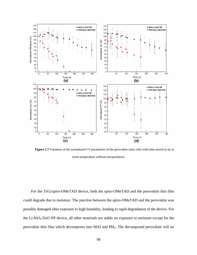
90
Figure 5.7 Variation of the normalized I-V parameters of the perovskite solar cells with time stored in air at
room temperature without encapsulation.
For the TiO2/spiro-OMeTAD device, both the spiro-OMeTAD and the perovskite thin film
could degrade due to moisture. The junction between the spiro-OMeTAD and the perovskite was
possibly damaged after exposure to high humidity, leading to rapid degradation of the device. For
the Li:NiOx/ZnO NP device, all other materials are stable on exposure to moisture except for the
perovskite thin film which decomposes into MAI and PbI2. The decomposed perovskite will no
91
longer contribute to the photocurrent, resulting to lower JSC. Nevertheless, moisture is more likely
to damage the bulk perovskite through grain boundaries, leaving a large part of the surface of the
perovskite thin film intact. Therefore, the junction between the perovskite thin film and the ZnO
NP thin film has a chance to preserve its quality, resulting in a negligible degradation of VOC and
FF even if the devices were kept in air with a relative humidity of 48.5 % for 300 h. There are two
possible solutions to improve the stability of perovskite solar cells. First, a process capable of
depositing perovskite thin film with larger crystal size needs to be developed to reduce the number
of paths through which the moisture gets to the bulk perovskite. Second, the metal oxides with
decent ambient stability have obvious advantages over those organic CTLs. Their properties
should be further investigated and developed for perovskite solar cells.
As mentioned earlier, the conventional perovskite solar cell adopted a device structure which
have been developed for almost 20 years, while the device structure with all inorganic CTLs
proposed in this work is new. It is reasonable to expect that its performance would be significantly
improved with further optimization. As a hint, spiro-OMeTAD used in this work was doped with
a lithium salt, which is a common procedure to increase the conductivity of spiro-OMeTAD,
leading to higher performance of solid-state dye-sensitized solar cells (SSDSSCs) and perovskite
solar cells [157]. Doping of ZnO NPs, which will increase the conductivity of ZnO NPs [158],
could be a strategy to improve the efficiency of perovskite solar cells with the device structure
developed in this work.
92
FUTURE WORK AND CONCLUSION
6.1 FUTURE WORK
6.1.1 Interface Engineering of CZTS Solar Cells
As discussed earlier, while the defect density in perovskite solar cell is as high as 2.79×1016 cm-3,
more than 18% efficiency can still be obtained. Conversely, while the defect density in CZTS solar
cell is lower than what is observed in perovskite solar cell (1×1016 cm-3), the highest efficiency
obtained is less than 13%. This indicates that the quality of the CZTS absorber layer is not the
major factor which limits the performance of CZTS solar cell. The low quality of the interfaces,
including the interface between CdS and CZTS and the interface between CZTS and Mo, could be
the origins of the poor performance in CZTS solar cells.
The employment of CdS in CZTS solar cells was based on the experiences in developing
CIGS solar cells. Although CdS is reportedly to be the best n-type semiconductor to form p-n
junction in CZTS solar cells, it has yet to be optimized. Recently, it has been found that the built-
in homogeneous p-n junction observed in CIGS solar cell due to the diffusion of Cd into CIGS
thin film does not exist in CZTS solar cell [159, 160]. This indicates that the photo-excited
electrons and holes in CZTS must be separated by the heterogeneous p-n junction formed by CdS
and CZTS, leading to higher possibility to be recombined. The quality of the interface of
93
CdS/CZTS should be improved by using alternative n-type semiconductors or by developing
alternative coating processes for CdS thin films.
Similarly, the employment of Mo back contact in CZTS solar cells was also based on the
experiences in developing CIGS solar cells. However, it has been found that the coating procedures
which have worked pretty well with CIGS solar cell would resulted into formation of extremely
thick MoSe2 thin film, leading to high series resistance and deteriorated the device efficiency
[161]. Materials such as TiN and TiB2 have been deposited between the Mo and the CZTS to partly
or completely suppress the formation of MoSe2 thin film [162-164]. Other materials which will
sufficiently suppress the formation of MoSe2 and effectively facilitate the transport of charges
need to be explored.
6.1.2 Interface Engineering of MAPbI3 Solar Cells
Li doping has been applied to enhance the conductivity of organic HTLs such as spiro-OMeTAD
and P3HT, which greatly enhances the device efficiency of perovskite solar cells [157, 165]. For
inorganic HTL such as NiOx, Cu doping was reported to enhance its conductivity, leading to higher
efficiency of perovskite solar cells [166]. Al doping is well known to improve the conductivity of
ZnO thin films, ZnO nanorods, and ZnO nanoparticles [167-169]. The efficiency of solar cells was
improved by using these doped materials [168]. As addressed in 4.3, the application of ZnO NPs
as ETL has greatly improved the stability of perovskite solar cells. However, the efficiency lags
behind. This is probably caused by the extremely low conductivity of ZnO NPs. Therefore,
application of Al-doped ZnO NPs as ETL in perovskite solar cell can possibly improve both the
efficiency and the stability of perovskite solar cells.
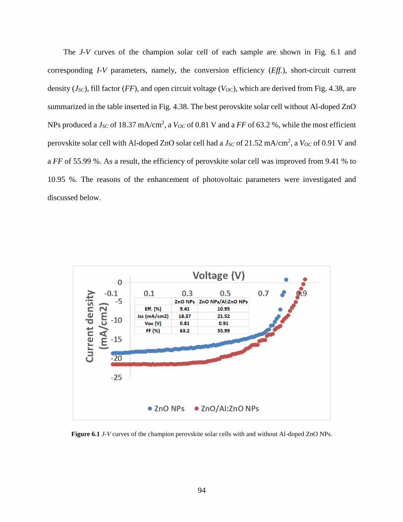
94
The J-V curves of the champion solar cell of each sample are shown in Fig. 6.1 and
corresponding I-V parameters, namely, the conversion efficiency (Eff.), short-circuit current
density (JSC), fill factor (FF), and open circuit voltage (VOC), which are derived from Fig. 4.38, are
summarized in the table inserted in Fig. 4.38. The best perovskite solar cell without Al-doped ZnO
NPs produced a JSC of 18.37 mA/cm2, a VOC of 0.81 V and a FF of 63.2 %, while the most efficient
perovskite solar cell with Al-doped ZnO solar cell had a JSC of 21.52 mA/cm2, a VOC of 0.91 V and
a FF of 55.99 %. As a result, the efficiency of perovskite solar cell was improved from 9.41 % to
10.95 %. The reasons of the enhancement of photovoltaic parameters were investigated and
discussed below.
Figure 6.1 J-V curves of the champion perovskite solar cells with and without Al-doped ZnO NPs.
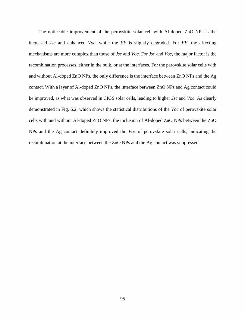
95
The noticeable improvement of the perovskite solar cell with Al-doped ZnO NPs is the
increased Jsc and enhanced Voc, while the FF is slightly degraded. For FF, the affecting
mechanisms are more complex than those of Jsc and Voc. For Jsc and Voc, the major factor is the
recombination processes, either in the bulk, or at the interfaces. For the perovskite solar cells with
and without Al-doped ZnO NPs, the only difference is the interface between ZnO NPs and the Ag
contact. With a layer of Al-doped ZnO NPs, the interface between ZnO NPs and Ag contact could
be improved, as what was observed in CIGS solar cells, leading to higher Jsc and Voc. As clearly
demonstrated in Fig. 6.2, which shows the statistical distributions of the Voc of perovskite solar
cells with and without Al-doped ZnO NPs, the inclusion of Al-doped ZnO NPs between the ZnO
NPs and the Ag contact definitely improved the Voc of perovskite solar cells, indicating the
recombination at the interface between the ZnO NPs and the Ag contact was suppressed.
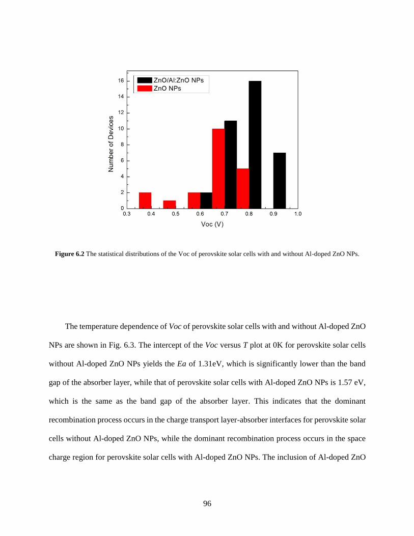
96
Figure 6.2 The statistical distributions of the Voc of perovskite solar cells with and without Al-doped ZnO NPs.
The temperature dependence of Voc of perovskite solar cells with and without Al-doped ZnO
NPs are shown in Fig. 6.3. The intercept of the Voc versus T plot at 0K for perovskite solar cells
without Al-doped ZnO NPs yields the Ea of 1.31eV, which is significantly lower than the band
gap of the absorber layer, while that of perovskite solar cells with Al-doped ZnO NPs is 1.57 eV,
which is the same as the band gap of the absorber layer. This indicates that the dominant
recombination process occurs in the charge transport layer-absorber interfaces for perovskite solar
cells without Al-doped ZnO NPs, while the dominant recombination process occurs in the space
charge region for perovskite solar cells with Al-doped ZnO NPs. The inclusion of Al-doped ZnO
97
NPs between the ZnO NPs and the Ag contact can improve the interface by suppressing the
interfacial recombination, leading to higher performance.
Figure 6.3 Temperature dependence of the Voc and its linear extrapolation line to 0 K for perovskite solar
cells with and without Al-doped ZnO NPs, which helps to elucidate the dominant recombination process in the two
types of devices.
While the utilization of Al-doped ZnO NPs can enhance the Voc of perovskite solar cells and
therefore increase the performance of perovskite solar cells, the efficiency obtained so far is still
lower than what has been obtained from perovskite solar cells with conventional structures.
98
Investigation on the cross section of the device using KPFM can possibly reveal how the charges
are transported and where the improvement could be achieved.
6.1.3 Effects of impurities in MAPbI3 Solar Cells
Cl doping has been demonstrated to be capable of effectively improve the performance of
perovskite solar cells. Furthermore, introduction of negligible amount of Cl into low purity
MAPbI3 solar cell can significantly boost the performance. Therefore, the concentration of Cl in
perovskite thin film will be investigated. Also, how and where Cl lies in perovskite thin film will
also be studied. Furthermore, the impurities in PbI2 will be revealed and their effects on the
performance of perovskite solar cells will be investigated. By combining theoretical calculations
with experimental results, the mechanisms behind the Cl doping-associated improvement of
performance of perovskite solar cells made from low purity PbI2 will be revealed. Doping of
perovskite thin films with alternative materials with expectation to enhance device performance
will be explored. The alternative doping procedures are expected to neutralize the impurities in
PbI2, passivate the grain boundaries of perovskite thin film, and improve the lifetime of the carriers.
6.2 CONCLUSION
The properties of the CZTS thin films deposited by the water-based method are greatly affected
by the Se feeding time. Varying the time from 0 to 30 min resulted in CZTS thin films with ratios
of Se/(Se+S) varying from 0 to 25%. The extension of Se vapor feeding time increases the
bandgap, slightly increases the lattice parameters, and significantly improves the morphologies of
99
the CZTS thin films. A remarkable enhancement of performance was achieved from the CZTS
solar cells with longer Se vapor feeding times compared to those without Se vapor feeding.
The mixed halide source method proposed in this work can be applied to combine the
advantages of a modified one-step process and Cl incorporation. A larger band bending at grain
boundaries with Cl incorporation, revealed by KPFM measurement, suggest that a p-i-n type of
heterojunction junction is formed in the devices with Cl incorporation. The p-i-n junction
facilitates the charge carrier collection and reduces recombination. Planar perovskite solar cells
with uniform morphology can be fabricated by the two-step solution process and the performance
can be improved by the Cl incorporation. This technique can be easily combined with other highly
efficient growth methods. Higher performance could be expected for solution-processed, planar
perovskite solar cells.
Additionally, we have successfully prepared inorganic metal oxides which can be used as
CTLs in highly performed perovskite solar cells. The stability of the perovskite solar cells has been
significantly enhanced due to the stability of these inorganic metal oxides in ambient environment.
The slow degradation observed in corresponding perovskite solar cells was suggested to be mainly
caused by the moisture infiltrated into the perovskite thin film through grain boundaries, while the
rapid loss of performance observed in the conventional perovskite solar cell with device structure
of TiO2/spiro-OMeTAD resulted from the degradation of the perovskite thin film and the junction.
This study provides an excellent device structure for making highly stable and efficient perovskite
solar cells.
Finally, the defect density of CZTS solar cell is reported to be 1×1016 cm-3, while that of
perovskite solar cell is found to be more than 2×1016 cm-3. Although the defect density in
perovskite solar cell is higher than that in CZTS solar cell, the efficiency obtained so far from

100
perovskite solar cell is much higher than that obtained from CZTS solar cell. This indicates that
the quality of the interfaces in CZTS solar cell is much worse than that of perovskite solar cell,
and should be prioritized in the future work.
101
BIBLIOGRAPHY
[1] Available: http://www1.umn.edu/iree/e3/archive/archive_2010/E3_Aydil.pdf
[2] M. A. Green, "Estimates of Te and In Prices from Direct Mining of Known Ores," Progress
in Photovoltaics, vol. 17, pp. 347-359, Aug 2009.
[3] W. Wang, M. T. Winkler, O. Gunawan, T. Gokmen, T. K. Todorov, Y. Zhu, et al., "Device
Characteristics of CZTSSe Thin-Film Solar Cells with 12.6% Efficiency," Advanced
Energy Materials, vol. 4, May 2014.
[4] N. J. Jeon, J. H. Noh, W. S. Yang, Y. C. Kim, S. Ryu, J. Seo, et al., "Compositional
engineering of perovskite materials for high-performance solar cells," Nature, vol. 517, pp.
476-480, 01/22/print 2015.
[5] S. Wagner and P. M. Bridenbaugh, "Multicomponent tetrahedral compounds for solar
cells," Journal of Crystal Growth, vol. 39, pp. 151-159, 7// 1977.
[6] I. Kentaro and N. Tatsuo, "Electrical and Optical Properties of Stannite-Type Quaternary
Semiconductor Thin Films," Japanese Journal of Applied Physics, vol. 27, p. 2094, 1988.
[7] H. Katagiri, N. Sasaguchi, S. Hando, S. Hoshino, J. Ohashi, and T. Yokota, "Preparation
and evaluation of Cu2ZnSnS4 thin films by sulfurization of E B evaporated precursors,"
Solar Energy Materials and Solar Cells, vol. 49, pp. 407-414, 12// 1997.
[8] R. Haight, A. Barkhouse, O. Gunawan, B. Shin, M. Copel, M. Hopstaken, et al., "Band
alignment at the Cu2ZnSn(SxSe1-x)4/CdS interface," Applied Physics Letters, vol. 98, Jun
20 2011.
[9] S. Y. Chen, J. H. Yang, X. G. Gong, A. Walsh, and S. H. Wei, "Intrinsic point defects and
complexes in the quaternary kesterite semiconductor Cu2ZnSnS4," Physical Review B, vol.
81, Jun 8 2010.
[10] P. Jackson, D. Hariskos, R. Wuerz, O. Kiowski, A. Bauer, T. M. Friedlmeier, et al.,
"Properties of Cu(In,Ga)Se2 solar cells with new record efficiencies up to 21.7%," Physica
Status Solidi-Rapid Research Letters, vol. 9, pp. 28-31, Jan 2015.
102
[11] L. Yin, G. M. Cheng, Y. Feng, Z. H. Li, C. L. Yang, and X. D. Xiao, "Limitation factors for the performance of kesterite Cu2ZnSnS4 thin film solar cells studied by defect characterization," Rsc Advances, vol. 5, pp. 40369-40374, 2015.
[12] A. Kojima, K. Teshima, Y. Shirai, and T. Miyasaka, "Organometal Halide Perovskites as Visible-Light Sensitizers for Photovoltaic Cells," Journal of the American Chemical Society, vol. 131, pp. 6050-6051, 2009/05/06 2009.
[13] J.-H. Im, C.-R. Lee, J.-W. Lee, S.-W. Park, and N.-G. Park, "6.5% efficient perovskite quantum-dot-sensitized solar cell," Nanoscale, vol. 3, pp. 4088-4093, 2011.
[14] H.-S. Kim, C.-R. Lee, J.-H. Im, K.-B. Lee, T. Moehl, A. Marchioro, et al., "Lead Iodide Perovskite Sensitized All-Solid-State Submicron Thin Film Mesoscopic Solar Cell with Efficiency Exceeding 9%," Sci. Rep., vol. 2, 08/21/online 2012.
[15] J. Burschka, N. Pellet, S.-J. Moon, R. Humphry-Baker, P. Gao, M. K. Nazeeruddin, et al., "Sequential deposition as a route to high-performance perovskite-sensitized solar cells," Nature, vol. 499, pp. 316-319, 07/18/print 2013.
[16] M. Liu, M. B. Johnston, and H. J. Snaith, "Efficient planar heterojunction perovskite solar cells by vapour deposition," Nature, vol. 501, pp. 395-398, 09/19/print 2013.
[17] M. Xiao, F. Huang, W. Huang, Y. Dkhissi, Y. Zhu, J. Etheridge, et al., "A Fast Deposition-
Crystallization Procedure for Highly Efficient Lead Iodide Perovskite Thin-Film Solar Cells," Angewandte Chemie International Edition, vol. 53, pp. 9898-9903, 2014.
[18] C.-W. Chen, H.-W. Kang, S.-Y. Hsiao, P.-F. Yang, K.-M. Chiang, and H.-W. Lin, "Efficient and Uniform Planar-Type Perovskite Solar Cells by Simple Sequential Vacuum Deposition," Advanced Materials, vol. 26, pp. 6647-6652, 2014.
[19] J.-W. Lee, D.-J. Seol, A.-N. Cho, and N.-G. Park, "High-Efficiency Perovskite Solar Cells Based on the Black Polymorph of HC(NH2)2PbI3," Advanced Materials, vol. 26, pp.
4991-4998, 2014.
[20] A. Suzuki, H. Okada, and T. Oku, "Fabrication and Characterization of CH3NH3PbI3-x-
yBrxCly Perovskite Solar Cells," Energies, vol. 9, May 2016.
[21] C. C. Chen, Z. R. Hong, G. Li, Q. Chen, H. P. Zhou, and Y. Yang, "One-step, low-
temperature deposited perovskite solar cell utilizing small molecule additive," Journal of Photonics for Energy, vol. 5, Jan 16 2015.
[22] D. Vak, K. Hwang, A. Faulks, Y.-S. Jung, N. Clark, D.-Y. Kim, et al., "3D Printer Based Slot-Die Coater as a Lab-to-Fab Translation Tool for Solution-Processed Solar Cells," Advanced Energy Materials, vol. 5, pp. n/a-n/a, 2015.
103
[23] M. Lv, X. Dong, X. Fang, B. Lin, S. Zhang, J. Ding, et al., "A promising alternative solvent of perovskite to induce rapid crystallization for high-efficiency photovoltaic devices," RSC Advances, vol. 5, pp. 20521-20529, 2015.
[24] P.-W. Liang, C.-Y. Liao, C.-C. Chueh, F. Zuo, S. T. Williams, X.-K. Xin, et al., "Additive Enhanced Crystallization of Solution-Processed Perovskite for Highly Efficient Planar-
Heterojunction Solar Cells," Advanced Materials, vol. 26, pp. 3748-3754, 2014.
[25] D. Yang, Z. Yang, W. Qin, Y. Zhang, S. Liu, and C. Li, "Alternating precursor layer deposition for highly stable perovskite films towards efficient solar cells using vacuum deposition," Journal of Materials Chemistry A, vol. 3, pp. 9401-9405, 2015.
[26] H. Zhou, Q. Chen, G. Li, S. Luo, T.-b. Song, H.-S. Duan, et al., "Interface engineering of highly efficient perovskite solar cells," Science, vol. 345, pp. 542-546, August 1, 2014 2014.
[27] S. N. Habisreutinger, T. Leijtens, G. E. Eperon, S. D. Stranks, R. J. Nicholas, and H. J. Snaith, "Carbon Nanotube/Polymer Composites as a Highly Stable Hole Collection Layer in Perovskite Solar Cells," Nano Letters, vol. 14, pp. 5561-5568, 2014/10/08 2014.
[28] J. H. Noh, S. H. Im, J. H. Heo, T. N. Mandal, and S. I. Seok, "Chemical Management for Colorful, Efficient, and Stable Inorganic-Organic Hybrid Nanostructured Solar Cells," Nano Letters, vol. 13, pp. 1764-1769, Apr 2013.
[29] Y. Yamada, T. Nakamura, M. Endo, A. Wakamiya, and Y. Kanemitsu, "Photocarrier Recombination Dynamics in Perovskite CH3NH3PbI3 for Solar Cell Applications," Journal of the American Chemical Society, vol. 136, pp. 11610-11613, 2014/08/20 2014.
[30] M. Powalla, M. Cemernjak, J. Eberhardt, F. Kessler, R. Kniese, H. D. Mohring, et al., "Large-area CIGS modules: Pilot line production and new developments," Solar Energy Materials and Solar Cells, vol. 90, pp. 3158-3164, Nov 23 2006.
[31] C. S. Jiang, R. Noufi, J. A. AbuShama, K. Ramanathan, H. R. Moutinho, J. Pankow, et al., "Local built-in potential on grain boundary of Cu(In,Ga)Se2 thin films," Applied Physics Letters, vol. 84, pp. 3477-3479, May 3 2004.
[32] I. Visoly-Fisher, S. R. Cohen, K. Gartsman, A. Ruzin, and D. Cahen, "Understanding the beneficial role of grain boundaries in polycrystalline solar cells from single-grain-boundary scanning probe microscopy," Advanced Functional Materials, vol. 16, pp. 649-660, Mar 20 2006.
[33] A. Zaban, M. Greenshtein, and J. Bisquert, "Determination of the Electron Lifetime in Nanocrystalline Dye Solar Cells by Open-Circuit Voltage Decay Measurements," ChemPhysChem, vol. 4, pp. 859-864, 2003.
104
[34] S. R. Lederhandler and L. J. Giacoletto, "Measurement of Minority Carrier Lifetime and Surface Effects in Junction Devices," Proceedings of the Institute of Radio Engineers, vol. 43, pp. 477-483, 1955.
[35] T. Pisarkiewicz, "Photodecay method in investigation of materials and photovoltaic structures," Opto-Electronics Review, vol. 12, pp. 33-40, Mar 2004.
[36] G. P. Li and K. L. Wang, "Detection Sensitivity and Spatial-Resolution of Reverse-Bias Pulsed Deep-Level Transient Spectroscopy for Studying Electric Field-Enhanced Carrier Emission," Journal of Applied Physics, vol. 57, pp. 1016-1021, 1985.
[37] J. H. a. P. Zabierowski, Advanced Characterization Techniques for Thin Film Solar Cells: Wiley-VCH, 2011.
[38] A. Jasenek, U. Rau, V. Nadenau, and H. W. Schock, "Electronic properties of CuGaSe2-
based heterojunction solar cells. Part II. Defect spectroscopy," Journal of Applied Physics, vol. 87, pp. 594-602, 2000.
[39] M. Rusu, W. Eisele, R. Wurz, A. Ennaoui, M. C. Lux-Steiner, T. P. Niesen, et al., "Current transport in ZnO/ZnS/Cu(In,Ga)(S,Se)2 solar cell," Journal of Physics and Chemistry of Solids, vol. 64, pp. 2037-2040, Sep-Oct 2003.
[40] D. B. Mitzi, O. Gunawan, T. K. Todorov, and D. A. R. Barkhouse, Prospects and performance limitations for Cu–Zn–Sn–S–Se photovoltaic technology vol. 371, 2013.
[41] A. Doukkali, S. Ledain, C. Guasch, and J. Bonnet, "Surface potential mapping of biased pn junction with kelvin probe force microscopy: application to cross-section devices," Applied surface science, vol. 235, pp. 507-512, 2004.
[42] F. Lan and G. Li, "Direct Observation of Hole Transfer from Semiconducting Polymer to Carbon Nanotubes," Nano Letters, vol. 13, pp. 2086-2091, 2013/05/08 2013.
[43] C.-S. Jiang, M. Yang, Y. Zhou, B. To, S. U. Nanayakkara, J. M. Luther, et al., "Carrier separation and transport in perovskite solar cells studied by nanometre-scale profiling of electrical potential," Nature communications, vol. 6, 2015.
[44] R. Saive, M. Scherer, C. Mueller, D. Daume, J. Schinke, M. Kroeger, et al., "Imaging the electric potential within organic solar cells," Advanced Functional Materials, vol. 23, pp. 5854-5860, 2013.
[45] Q. Chen, L. Mao, Y. Li, T. Kong, N. Wu, C. Ma, et al., "Quantitative operando visualization of the energy band depth profile in solar cells," Nature communications, vol. 6, 2015.
[46] G. Li, B. Mao, F. Lan, and L. Liu, "Practical aspects of single-pass scan Kelvin probe force microscopy," Review of Scientific Instruments, vol. 83, p. 113701, 2012.
105
[47] W. Wang, M. T. Winkler, O. Gunawan, T. Gokmen, T. K. Todorov, Y. Zhu, et al., "Device
Characteristics of CZTSSe Thin-Film Solar Cells with 12.6% Efficiency," Advanced
Energy Materials, vol. 4, pp. n/a-n/a, 2014.
[48] I. Repins, C. Beall, N. Vora, C. DeHart, D. Kuciauskas, P. Dippo, et al., "Co-evaporated
Cu2ZnSnSe4 films and devices," Solar Energy Materials and Solar Cells, vol. 101, pp.
154-159, 6// 2012.
[49] K. Woo, Y. Kim, and J. Moon, "A non-toxic, solution-processed, earth abundant absorbing
layer for thin-film solar cells," Energy & Environmental Science, vol. 5, pp. 5340-5345,
2012.
[50] Y. Sun, Y. Zhang, H. Wang, M. Xie, K. Zong, H. Zheng, et al., "Novel non-hydrazine
solution processing of earth-abundant Cu2ZnSn(S,Se)4 absorbers for thin-film solar cells,"
Journal of Materials Chemistry A, vol. 1, pp. 6880-6887, 2013.
[51] Q. Guo, G. M. Ford, W.-C. Yang, B. C. Walker, E. A. Stach, H. W. Hillhouse, et al.,
"Fabrication of 7.2% Efficient CZTSSe Solar Cells Using CZTS Nanocrystals," Journal of
the American Chemical Society, vol. 132, pp. 17384-17386, 2010/12/15 2010.
[52] W. Yang, H.-S. Duan, K. C. Cha, C.-J. Hsu, W.-C. Hsu, H. Zhou, et al., "Molecular
Solution Approach To Synthesize Electronic Quality Cu2ZnSnS4 Thin Films," Journal of
the American Chemical Society, vol. 135, pp. 6915-6920, 2013/05/08 2013.
[53] W. Yang, H.-S. Duan, B. Bob, H. Zhou, B. Lei, C.-H. Chung, et al., "Novel Solution
Processing of High-Efficiency Earth-Abundant Cu2ZnSn(S,Se)4 Solar Cells," Advanced
Materials, vol. 24, pp. 6323-6329, 2012.
[54] Y. Cao, M. S. Denny, J. V. Caspar, W. E. Farneth, Q. Guo, A. S. Ionkin, et al., "High-
Efficiency Solution-Processed Cu2ZnSn(S,Se)4 Thin-Film Solar Cells Prepared from
Binary and Ternary Nanoparticles," Journal of the American Chemical Society, vol. 134,
pp. 15644-15647, 2012/09/26 2012.
[55] W. Ki and H. W. Hillhouse, "Earth-Abundant Element Photovoltaics Directly from Soluble
Precursors with High Yield Using a Non-Toxic Solvent," Advanced Energy Materials, vol.
1, pp. 732-735, 2011.
[56] J. Minlin, R. Dhakal, L. Yong, P. Thapaliya, and Y. Xingzhong, "Cu2ZnSnS4 (CZTS)
polycrystalline thin films prepared by sol-gel method," in Photovoltaic Specialists
Conference (PVSC), 2011 37th IEEE, 2011, pp. 001283-001286.
[57] M. Jiang, Y. Li, R. Dhakal, P. Thapaliya, M. Mastro, J. D. Caldwell, et al., "Cu2ZnSnS4
polycrystalline thin films with large densely packed grains prepared by sol-gel method,"
Journal of Photonics for Energy, vol. 1, pp. 019501-019501-6, 2011.
[58] J. Minlin, W. Fanan, L. Fei, L. Guangyong, and Y. Xingzhong, "Bandgap tuning and
morphology amelioration of sol-gel derived Cu2ZnSnS4 (CZTS) thin films by selenium
106
incorporation," in Photovoltaic Specialists Conference (PVSC), 2013 IEEE 39th, 2013, pp.
2602-2604.
[59] M. Jiang, F. Lan, X. Yan, and G. Li, "Cu2ZnSn(S1–xSex)4 thin film solar cells prepared by
water-based solution process," physica status solidi (RRL) – Rapid Research Letters, vol.
8, pp. 223-227, 2014.
[60] M. Jiang, K. Tang, and X. Yan, "Characterization of intrinsic ZnO thin film deposited by sputtering and its effects on CuIn1−xGaxSe2 solar cells," Journal of Photonics for Energy,
vol. 2, pp. 028502-1-028502-11, 2012.
[61] C. J. Doona and D. M. Stanbury, "Equilibrium and Redox Kinetics of Copper(II)
−Thiourea Complexes," Inorganic Chemistry, vol. 35, pp. 3210-3216, 1996/01/01 1996.
[62] P. Bombicz, I. Mutikainen, M. Krunks, T. Leskelä, J. Madarász, and L. Niinistö,
"Synthesis, vibrational spectra and X-ray structures of copper(I) thiourea complexes,"
Inorganica Chimica Acta, vol. 357, pp. 513-525, 1/30/ 2004.
[63] J. Madarász, P. Bombicz, M. Okuya, and S. Kaneko, "Thermal decomposition of thiourea
complexes of Cu(I), Zn(II), and Sn(II) chlorides as precursors for the spray pyrolysis
deposition of sulfide thin films," Solid State Ionics, vol. 141–142, pp. 439-446, 5/1/ 2001.
[64] A. Weber, R. Mainz, T. Unold, S. Schorr, and H.-W. Schock, "In-situ XRD on formation
reactions of Cu2ZnSnS4 thin films," physica status solidi (c), vol. 6, pp. 1245-1248, 2009.
[65] S. Chen, J.-H. Yang, X. G. Gong, A. Walsh, and S.-H. Wei, "Intrinsic point defects and
complexes in the quaternary kesterite semiconductor CuZnSnS4," Physical Review B, vol.
81, p. 245204, 06/08/ 2010.
[66] P. M. P. Salomé, P. A. Fernandes, and A. F. d. Cunha, "Influence of selenization pressure
on the growth of Cu2ZnSnSe4 films from stacked metallic layers," physica status solidi (c),
vol. 7, pp. 913-916, 2010.
[67] P. M. P. Salomé, P. A. Fernandes, A. F. da Cunha, J. P. Leitão, J. Malaquias, A. Weber, et
al., "Growth pressure dependence of Cu2ZnSnSe4 properties," Solar Energy Materials and
Solar Cells, vol. 94, pp. 2176-2180, 12// 2010.
[68] A. Weber, R. Mainz, and H. W. Schock, "On the Sn loss from thin films of the material
system Cu–Zn–Sn–S in high vacuum," Journal of Applied Physics, vol. 107, pp. -, 2010.
[69] A. Redinger, D. M. Berg, P. J. Dale, and S. Siebentritt, "The Consequences of Kesterite
Equilibria for Efficient Solar Cells," Journal of the American Chemical Society, vol. 133,
pp. 3320-3323, 2011/03/16 2011.
[70] K. Wang, O. Gunawan, T. Todorov, B. Shin, S. J. Chey, N. A. Bojarczuk, et al., "Thermally
evaporated Cu2ZnSnS4 solar cells," Applied Physics Letters, vol. 97, pp. -, 2010.
107
[71] A. Wangperawong, J. S. King, S. M. Herron, B. P. Tran, K. Pangan-Okimoto, and S. F.
Bent, "Aqueous bath process for deposition of Cu2ZnSnS4 photovoltaic absorbers," Thin
Solid Films, vol. 519, pp. 2488-2492, 2/1/ 2011.
[72] R. J. Deokate, A. D. Adsool, N. S. Shinde, S. M. Pawar, and C. D. Lokhande, "Structural
and Optical Properties of Spray-deposited Cu2ZnSnS4 thin Films," Energy Procedia, vol.
54, pp. 627-633, // 2014.
[73] S. C. Riha, B. A. Parkinson, and A. L. Prieto, "Compositionally Tunable Cu2ZnSn(S1–
xSex)4 Nanocrystals: Probing the Effect of Se-Inclusion in Mixed Chalcogenide Thin
Films," Journal of the American Chemical Society, vol. 133, pp. 15272-15275, 2011/10/05
2011.
[74] K. Wang, O. Gunawan, T. Todorov, B. Shin, S. J. Chey, N. A. Bojarczuk, et al., "Thermally
evaporated Cu2ZnSnS4 solar cells," Applied Physics Letters, vol. 97, pp. 143508-143508-
3, 2010.
[75] I. P. Parkin, L. S. Price, T. G. Hibbert, and K. C. Molloy, "The first single source deposition
of tin sulfide coatings on glass: aerosol-assisted chemical vapour deposition using
[Sn(SCHCHS)]," Journal of Materials Chemistry, vol. 11, pp. 1486-1490, 2001.
[76] L. A. Isac, A. Duta, A. Kriza, I. A. Enesca, and M. Nanu, "The growth of CuS thin films
by Spray Pyrolysis," Journal of Physics: Conference Series, vol. 61, p. 477, 2007.
[77] M. Bär, B.-A. Schubert, B. Marsen, R. G. Wilks, S. Pookpanratana, M. Blum, et al., "Cliff-
like conduction band offset and KCN-induced recombination barrier enhancement at the
CdS/Cu2ZnSnS4 thin-film solar cell heterojunction," Applied Physics Letters, vol. 99, pp.
-, 2011.
[78] M. Grossberg, J. Krustok, J. Raudoja, K. Timmo, M. Altosaar, and T. Raadik,
"Photoluminescence and Raman study of Cu2ZnSn(SexS1−x)4 monograins for photovoltaic
applications," Thin Solid Films, vol. 519, pp. 7403-7406, 8/31/ 2011.
[79] M. Bär, B.-A. Schubert, B. Marsen, S. Krause, S. Pookpanratana, T. Unold, et al., "Impact
of KCN etching on the chemical and electronic surface structure of Cu2ZnSnS4 thin-film
solar cell absorbers," Applied Physics Letters, vol. 99, pp. -, 2011.
[80] N. B. Chaure, S. Bordas, A. P. Samantilleke, S. N. Chaure, J. Haigh, and I. M. Dharmadasa,
"Investigation of electronic quality of chemical bath deposited cadmium sulphide layers
used in thin film photovoltaic solar cells," Thin Solid Films, vol. 437, pp. 10-17, 8/1/ 2003.
[81] A. Fairbrother, E. García-Hemme, V. Izquierdo-Roca, X. Fontané, F. A. Pulgarín-Agudelo,
O. Vigil-Galán, et al., "Development of a Selective Chemical Etch To Improve the
Conversion Efficiency of Zn-Rich Cu2ZnSnS4 Solar Cells," Journal of the American
Chemical Society, vol. 134, pp. 8018-8021, 2012/05/16 2012.
108
[82] G. Zoppi, I. Forbes, R. W. Miles, P. J. Dale, J. J. Scragg, and L. M. Peter, "Cu2ZnSnSe4
thin film solar cells produced by selenisation of magnetron sputtered precursors," Progress
in Photovoltaics: Research and Applications, vol. 17, pp. 315-319, 2009.
[83] M. Bär, W. Bohne, J. Röhrich, E. Strub, S. Lindner, M. C. Lux-Steiner, et al.,
"Determination of the band gap depth profile of the penternary Cu(In(1−X)GaX)(SYSe(1−Y))2
chalcopyrite from its composition gradient," Journal of Applied Physics, vol. 96, pp. 3857-
3860, 2004.
[84] H. Wei, Z. Ye, M. Li, Y. Su, Z. Yang, and Y. Zhang, "Tunable band gap Cu2ZnSnS4xSe4(1-
x) nanocrystals: experimental and first-principles calculations," CrystEngComm, vol. 13,
pp. 2222-2226, 2011.
[85] D. A. R. Barkhouse, O. Gunawan, T. Gokmen, T. K. Todorov, and D. B. Mitzi, "Device
characteristics of a 10.1% hydrazine-processed Cu2ZnSn(Se,S)4 solar cell," Progress in
Photovoltaics: Research and Applications, vol. 20, pp. 6-11, 2012.
[86] T. K. Todorov, J. Tang, S. Bag, O. Gunawan, T. Gokmen, Y. Zhu, et al., "Beyond 11%
Efficiency: Characteristics of State-of-the-Art Cu2ZnSn(S,Se)4 Solar Cells," Advanced
Energy Materials, vol. 3, pp. 34-38, 2013.
[87] S. Ye, X. Tan, M. Jiang, B. Fan, K. Tang, and S. Zhuang, "Impact of different Na-
incorporating methods on Cu(In,Ga)Se2 thin film solar cells with a low-Na substrate,"
Applied Optics, vol. 49, pp. 1662-1665, 2010/03/20 2010.
[88] V. D’Innocenzo, G. Grancini, M. J. P. Alcocer, A. R. S. Kandada, S. D. Stranks, M. M.
Lee, et al., "Excitons versus free charges in organo-lead tri-halide perovskites," Nat
Commun, vol. 5, 04/08/online 2014.
[89] N. Ahn, D. Y. Son, I. H. Jang, S. M. Kang, M. Choi, and N. G. Park, "Highly Reproducible
Perovskite Solar Cells with Average Efficiency of 18.3% and Best Efficiency of 19.7%
Fabricated via Lewis Base Adduct of Lead(II) Iodide," Journal of the American Chemical
Society, vol. 137, pp. 8696-8699, Jul 15 2015.
[90] G. E. Eperon, V. M. Burlakov, P. Docampo, A. Goriely, and H. J. Snaith, "Morphological
Control for High Performance, Solution-Processed Planar Heterojunction Perovskite Solar
Cells," Advanced Functional Materials, vol. 24, pp. 151-157, 2014.
[91] Y. Ogomi, A. Morita, S. Tsukamoto, T. Saitho, N. Fujikawa, Q. Shen, et al.,
"CH3NH3SnxPb(1-x)I3 Perovskite Solar Cells Covering up to 1060 nm," Journal of Physical
Chemistry Letters, vol. 5, pp. 1004-1011, Mar 20 2014.
[92] D. Q. Bi, A. M. El-Zohry, A. Hagfeldt, and G. Boschloo, "Unraveling the Effect of PbI2
Concentration on Charge Recombination Kinetics in Perovskite Solar Cells," Acs
Photonics, vol. 2, pp. 589-594, May 2015.
109
[93] Z. Xiao, C. Bi, Y. Shao, Q. Dong, Q. Wang, Y. Yuan, et al., "Efficient, high yield
perovskite photovoltaic devices grown by interdiffusion of solution-processed precursor
stacking layers," Energy & Environmental Science, vol. 7, pp. 2619-2623, 2014.
[94] J. M. Ball, M. M. Lee, A. Hey, and H. J. Snaith, "Low-temperature processed meso-
superstructured to thin-film perovskite solar cells," Energy & Environmental Science, vol.
6, pp. 1739-1743, 2013.
[95] E. Edri, S. Kirmayer, A. Henning, S. Mukhopadhyay, K. Gartsman, Y. Rosenwaks, et al.,
"Why Lead Methylammonium Tri-Iodide Perovskite-Based Solar Cells Require a
Mesoporous Electron Transporting Scaffold (but Not Necessarily a Hole Conductor),"
Nano Letters, vol. 14, pp. 1000-1004, Feb 2014.
[96] Z. G. Xiao, C. Bi, Y. C. Shao, Q. F. Dong, Q. Wang, Y. B. Yuan, et al., "Efficient, high
yield perovskite photovoltaic devices grown by interdiffusion of solution-processed
precursor stacking layers," Energy & Environmental Science, vol. 7, pp. 2619-2623, Aug
2014.
[97] S. L. Ye, X. H. Tan, M. L. Jiang, B. Fan, K. Tang, and S. L. Zhuang, "Impact of different
Na-incorporating methods on Cu(In,Ga)Se2 thin film solar cells with a low-Na substrate,"
Applied Optics, vol. 49, pp. 1662-1665, Mar 20 2010.
[98] S. D. Stranks, G. E. Eperon, G. Grancini, C. Menelaou, M. J. P. Alcocer, T. Leijtens, et al.,
"Electron-Hole Diffusion Lengths Exceeding 1 Micrometer in an Organometal Trihalide
Perovskite Absorber," Science, vol. 342, pp. 341-344, October 18, 2013 2013.
[99] G. Xing, N. Mathews, S. Sun, S. S. Lim, Y. M. Lam, M. Grätzel, et al., "Long-Range
Balanced Electron- and Hole-Transport Lengths in Organic-Inorganic CH3NH3PbI3,"
Science, vol. 342, pp. 344-347, October 18, 2013 2013.
[100] Z. Djebbour, A. Darga, A. M. Dubois, D. Mencaraglia, N. Naghavi, J. F. Guillemoles, et
al., "Admittance spectroscopy of cadmium free CIGS solar cells heterointerfaces," Thin
Solid Films, vol. 511, pp. 320-324, Jul 26 2006.
[101] Y. Y. Proskuryakov, K. Durose, B. M. Taele, G. P. Welch, and S. Oelting, "Admittance
spectroscopy of CdTe/CdS solar cells subjected to varied nitric-phosphoric etching
conditions," Journal of Applied Physics, vol. 101, Jan 1 2007.
[102] J. V. Li and D. H. Levi, "Determining the defect density of states by temperature derivative
admittance spectroscopy," Journal of Applied Physics, vol. 109, Apr 15 2011.
[103] M. Samiee, S. Konduri, B. Ganapathy, R. Kottokkaran, H. A. Abbas, A. Kitahara, et al.,
"Defect density and dielectric constant in perovskite solar cells," Applied Physics Letters,
vol. 105, Oct 13 2014.
110
[104] H. S. Duan, H. P. Zhou, Q. Chen, P. Y. Sun, S. Luo, T. B. Song, et al., "The identification
and characterization of defect states in hybrid organic-inorganic perovskite photovoltaics,"
Physical Chemistry Chemical Physics, vol. 17, pp. 112-116, 2015.
[105] H. B. Xu, R. J. Hong, B. Ai, L. Zhuang, and H. Shen, "Application of phosphorus diffusion
gettering process on upgraded metallurgical grade Si wafers and solar cells," Applied
Energy, vol. 87, pp. 3425-3430, Nov 2010.
[106] M. T. Zarmai, N. N. Ekere, C. F. Oduoza, and E. H. Amalu, "A review of interconnection
technologies for improved crystalline silicon solar cell photovoltaic module assembly,"
Applied Energy, vol. 154, pp. 173-182, Sep 15 2015.
[107] S. G. Chen, "An efficient sizing method for a stand-alone PV system in terms of the
observed block extremes," Applied Energy, vol. 91, pp. 375-384, Mar 2012.
[108] G. F. Hou, H. H. Sun, Z. Y. Jiang, Z. Q. Pan, Y. B. Wang, X. D. Zhang, et al., "Life cycle
assessment of grid-connected photovoltaic power generation from crystalline silicon solar
modules in China," Applied Energy, vol. 164, pp. 882-890, Feb 15 2016.
[109] L. J. Geerligs and D. Macdonald, "Base doping and recombination activity of impurities in
crystalline silicon solar cells," Progress in Photovoltaics, vol. 12, pp. 309-316, Jun 2004.
[110] J. R. Davis, A. Rohatgi, R. H. Hopkins, P. D. Blais, P. Raichoudhury, J. R. Mccormick, et
al., "Impurities in Silicon Solar-Cells," Ieee Transactions on Electron Devices, vol. 27, pp.
677-687, 1980.
[111] J. W. Bishop, "Microplasma Breakdown and Hot-Spots in Silicon Solar-Cells," Solar
Cells, vol. 26, pp. 335-349, Sep 1989.
[112] G. Buzanich, M. Radtke, U. Reinholz, H. Riesemeier, A. F. Thunemann, and C. Streli,
"Impurities in multicrystalline silicon wafers for solar cells detected by synchrotron micro-
beam X-ray fluorescence analysis," Journal of Analytical Atomic Spectrometry, vol. 27,
pp. 1875-1881, Nov 2012.
[113] A. M. Salama and L. J. Cheng, "The Effects of Titanium Impurities in N+-P Silicon Solar-
Cells," Journal of the Electrochemical Society, vol. 127, pp. 1164-1167, 1980.
[114] W. P. Lee, E. P. Teh, H. K. Yow, C. L. Choong, and T. Y. Tou, "Enhanced gettering of
iron impurities in bulk silicon by using external direct current electric field," Journal of
Electronic Materials, vol. 34, pp. L25-L29, Jul 2005.
[115] M. I. Asghar, M. Yli-Koski, H. Savin, A. Haarahiltunen, H. Talvitie, and J. Sinkkonen,
"Competitive iron gettering between internal gettering sites and boron implantation in CZ-
silicon," Materials Science and Engineering B-Advanced Functional Solid-State
Materials, vol. 159-60, pp. 224-227, Mar 15 2009.
111
[116] M. L. Jiang, J. M. Wu, F. Lan, Q. Tao, D. Gao, and G. Y. Li, "Enhancing the performance
of planar organo-lead halide perovskite solar cells by using a mixed halide source," Journal
of Materials Chemistry A, vol. 3, pp. 963-967, 2015.
[117] A. Babayigit, D. D. Thanh, A. Ethirajan, J. Manca, M. Muller, H. G. Boyen, et al.,
"Assessing the toxicity of Pb- and Sn-based perovskite solar cells in model organism Danio
rerio," Scientific Reports, vol. 6, Jan 13 2016.
[118] L. Kaake, X. D. Dang, W. L. Leong, Y. Zhang, A. Heeger, and T. Q. Nguyen, "Effects of
Impurities on Operational Mechanism of Organic Bulk Heterojunction Solar Cells,"
Advanced Materials, vol. 25, pp. 1706-1712, Mar 25 2013.
[119] J. Y. Cho, K. H. Seo, B. H. Kang, and K. Y. Kim, "The Effect of the Purity of Raw
Materials on the Purity of Silicon Extracted by Solvent Refining and Centrifugation,"
Korean Journal of Metals and Materials, vol. 50, pp. 907-911, Dec 2012.
[120] J. J. Chang, H. Zhu, B. C. Li, F. H. Isikgor, Y. Hao, Q. H. Xu, et al., "Boosting the
performance of planar heterojunction perovskite solar cell by controlling the precursor
purity of perovskite materials," Journal of Materials Chemistry A, vol. 4, pp. 887-893,
2016.
[121] P. Docampo, F. C. Hanusch, S. D. Stranks, M. Doblinger, J. M. Feckl, M. Ehrensperger, et
al., "Solution Deposition-Conversion for Planar Heterojunction Mixed Halide Perovskite
Solar Cells," Advanced Energy Materials, vol. 4, Oct 7 2014.
[122] N. Tripathi, M. Yanagida, Y. Shirai, T. Masuda, L. Y. Han, and K. Miyano, "Hysteresis-
free and highly stable perovskite solar cells produced via a chlorine-mediated interdiffusion
method," Journal of Materials Chemistry A, vol. 3, pp. 12081-12088, 2015.
[123] H. Yu, F. Wang, F. Y. Xie, W. W. Li, J. Chen, and N. Zhao, "The Role of Chlorine in the
Formation Process of "CH3NH3PbI3-xClx" Perovskite," Advanced Functional Materials,
vol. 24, pp. 7102-7108, Dec 3 2014.
[124] S. R. Cowan, W. L. Leong, N. Banerji, G. Dennler, and A. J. Heeger, "Identifying a
Threshold Impurity Level for Organic Solar Cells: Enhanced First-Order Recombination
Via Well-Defined PC84BM Traps in Organic Bulk Heterojunction Solar Cells," Advanced
Functional Materials, vol. 21, pp. 3083-3092, Aug 23 2011.
[125] M. M. Mandoc, F. B. Kooistra, J. C. Hummelen, B. de Boer, and P. W. M. Blom, "Effect
of traps on the performance of bulk heterojunction organic solar cells," Applied Physics
Letters, vol. 91, Dec 24 2007.
[126] P. K. Johnson, J. T. Heath, J. D. Cohen, K. Ramanathan, and J. R. Sites, "A comparative
study of defect states in evaporated and selenized CIGS(S) solar cells," Progress in
Photovoltaics, vol. 13, pp. 579-586, Nov 2005.
112
[127] P. T. Erslev, J. W. Lee, W. N. Shafarman, and J. D. Cohen, "The influence of Na on
metastable defect kinetics in CIGS materials," Thin Solid Films, vol. 517, pp. 2277-2281,
Feb 2 2009.
[128] J. Serhan, Z. Djebbour, D. Mencaraglia, F. Couzinie-Devy, N. Barreau, and J. Kessler,
"Influence of Ga content on defects in CuInxGa1-xSe2 based solar cell absorbers
investigated by sub gap modulated photocurrent and admittance spectroscopy," Thin Solid
Films, vol. 519, pp. 7312-7316, Aug 31 2011.
[129] A. S. Gudovskikh, J. P. Kleider, R. Chouffot, N. A. Kalyuzhnyy, S. A. Mintairov, and V.
M. Lantratov, "III-phosphides heterojunction solar cell interface properties from
admittance spectroscopy," Journal of Physics D-Applied Physics, vol. 42, Aug 21 2009.
[130] M. H. Du, "Efficient carrier transport in halide perovskites: theoretical perspectives,"
Journal of Materials Chemistry A, vol. 2, pp. 9091-9098, 2014.
[131] Y. Z. Xu, L. F. Zhu, J. J. Shi, S. T. Lv, X. Xu, J. Y. Xiao, et al., "Efficient Hybrid
Mesoscopic Solar Cells with Morphology-Controlled CH3NH3PbI3-xClx Derived from
Two-Step Spin Coating Method," Acs Applied Materials & Interfaces, vol. 7, pp.
2242-2248, Feb 4 2015.
[132] J. Qing, H. T. Chandran, Y. H. Cheng, X. K. Liu, H. W. Li, S. W. Tsang, et al., "Chlorine
Incorporation for Enhanced Performance of Planar Perovskite Solar Cell Based on Lead
Acetate Precursor," Acs Applied Materials & Interfaces, vol. 7, pp. 23110-23116, Oct 21
2015.
[133] M. Jiang, J. Wu, G. Di, and G. Li, "Nanostructured solar cell based on solution processed
Cu2ZnSnS4 nanoparticles and vertically aligned ZnO nanorod array," physica status solidi
(RRL) – Rapid Research Letters, vol. 8, pp. 971-975, 2014.
[134] Y. Han, S. Meyer, Y. Dkhissi, K. Weber, J. M. Pringle, U. Bach, et al., "Degradation
observations of encapsulated planar CH3NH3PbI3 perovskite solar cells at high
temperatures and humidity," Journal of Materials Chemistry A, vol. 3, pp. 8139-8147,
2015.
[135] M. O. Reese, A. J. Morfa, M. S. White, N. Kopidakis, S. E. Shaheen, G. Rumbles, et al.,
"Pathways for the degradation of organic photovoltaic P3HT:PCBM based devices," Solar
Energy Materials and Solar Cells, vol. 92, pp. 746-752, 7// 2008.
[136] E. Voroshazi, B. Verreet, T. Aernouts, and P. Heremans, "Long-term operational lifetime
and degradation analysis of P3HT:PCBM photovoltaic cells," Solar Energy Materials and
Solar Cells, vol. 95, pp. 1303-1307, 5// 2011.
[137] O. Malinkiewicz, C. Roldán-Carmona, A. Soriano, E. Bandiello, L. Camacho, M. K.
Nazeeruddin, et al., "Metal-Oxide-Free Methylammonium Lead Iodide Perovskite-Based
Solar Cells: the Influence of Organic Charge Transport Layers," Advanced Energy
Materials, vol. 4, pp. n/a-n/a, 2014.
113
[138] J. Cui, F. Meng, H. Zhang, K. Cao, H. Yuan, Y. Cheng, et al., "CH3NH3PbI3-Based Planar
Solar Cells with Magnetron-Sputtered Nickel Oxide," ACS Applied Materials & Interfaces,
vol. 6, pp. 22862-22870, 2014/12/24 2014.
[139] J. H. Kim, P.-W. Liang, S. T. Williams, N. Cho, C.-C. Chueh, M. S. Glaz, et al., "High-
Performance and Environmentally Stable Planar Heterojunction Perovskite Solar Cells
Based on a Solution-Processed Copper-Doped Nickel Oxide Hole-Transporting Layer,"
Advanced Materials, vol. 27, pp. 695-701, 2015.
[140] C. Pacholski, A. Kornowski, and H. Weller, "Self-assembly of ZnO: From nanodots to
nanorods.," Abstracts of Papers of the American Chemical Society, vol. 224, pp. U351-
U351, Aug 18 2002.
[141] K. H. Kim, C. Takahashi, Y. Abe, and M. Kawamura, "Effects of Cu doping on nickel
oxide thin film prepared by sol-gel solution process," Optik, vol. 125, pp. 2899-2901, 2014.
[142] Y. Y. Zhou, M. J. Yang, W. W. Wu, A. L. Vasiliev, K. Zhu, and N. P. Padture, "Room-
temperature crystallization of hybrid-perovskite thin films via solvent-solvent extraction
for high-performance solar cells," Journal of Materials Chemistry A, vol. 3, pp. 8178-8184,
2015.
[143] I. Sta, M. Jlassi, M. Hajji, and H. Ezzaouia, "Structural, optical and electrical properties of
undoped and Li-doped NiO thin films prepared by sol–gel spin coating method," Thin Solid
Films, vol. 555, pp. 131-137, 3/31/ 2014.
[144] W. J. E. Beek, M. M. Wienk, M. Kemerink, X. Yang, and R. A. J. Janssen, "Hybrid Zinc
Oxide Conjugated Polymer Bulk Heterojunction Solar Cells," The Journal of Physical
Chemistry B, vol. 109, pp. 9505-9516, 2005/05/01 2005.
[145] J. B. Baxter and C. A. Schmuttenmaer, "Conductivity of ZnO Nanowires, Nanoparticles,
and Thin Films Using Time-Resolved Terahertz Spectroscopy†," The Journal of Physical
Chemistry B, vol. 110, pp. 25229-25239, 2006/12/01 2006.
[146] S. Ryu, J. H. Noh, N. J. Jeon, Y. Chan Kim, W. S. Yang, J. Seo, et al., "Voltage output of
efficient perovskite solar cells with high open-circuit voltage and fill factor," Energy &
Environmental Science, vol. 7, pp. 2614-2618, 2014.
[147] F. X. Xie, D. Zhang, H. Su, X. Ren, K. S. Wong, M. Grätzel, et al., "Vacuum-Assisted
Thermal Annealing of CH3NH3PbI3 for Highly Stable and Efficient Perovskite Solar
Cells," ACS Nano, vol. 9, pp. 639-646, 2015/01/27 2015.
[148] I. A. Garduño, J. C. Alonso, M. Bizarro, R. Ortega, L. Rodríguez-Fernández, and A. Ortiz,
"Optical and electrical properties of lithium doped nickel oxide films deposited by spray
pyrolysis onto alumina substrates," Journal of Crystal Growth, vol. 312, pp. 3276-3281,
11/1/ 2010.
114
[149] C.-Y. Chang, C.-Y. Chu, Y.-C. Huang, C.-W. Huang, S.-Y. Chang, C.-A. Chen, et al.,
"Tuning Perovskite Morphology by Polymer Additive for High Efficiency Solar Cell,"
ACS Applied Materials & Interfaces, vol. 7, pp. 4955-4961, 2015/03/04 2015.
[150] M. K. Debanath and S. Karmakar, "Study of blueshift of optical band gap in zinc oxide
(ZnO) nanoparticles prepared by low-temperature wet chemical method," Materials
Letters, vol. 111, pp. 116-119, 11/15/ 2013.
[151] S. Shayesteh and A. Dizgah, "Effect of doping and annealing on the physical properties of
ZnO:Mg nanoparticles," Pramana, vol. 81, pp. 319-330, 2013/08/01 2013.
[152] C. J. Brabec, A. Cravino, D. Meissner, N. S. Sariciftci, T. Fromherz, M. T. Rispens, et al.,
"Origin of the Open Circuit Voltage of Plastic Solar Cells," Advanced Functional
Materials, vol. 11, pp. 374-380, 2001.
[153] M. Jiang, J. Wu, F. Lan, Q. Tao, D. Gao, and G. Li, "Enhancing the performance of planar
organo-lead halide perovskite solar cells by using a mixed halide source," Journal of
Materials Chemistry A, vol. 3, pp. 963-967, 2015.
[154] U. Bach, D. Lupo, P. Comte, J. E. Moser, F. Weissortel, J. Salbeck, et al., "Solid-state dye-
sensitized mesoporous TiO2 solar cells with high photon-to-electron conversion
efficiencies," Nature, vol. 395, pp. 583-585, 10/08/print 1998.
[155] M. Xiao, F. Huang, W. Huang, Y. Dkhissi, Y. Zhu, J. Etheridge, et al., "A Fast Deposition-
Crystallization Procedure for Highly Efficient Lead Iodide Perovskite Thin-Film Solar
Cells," Angewandte Chemie, vol. 126, pp. 10056-10061, 2014.
[156] L. Yang, U. B. Cappel, E. L. Unger, M. Karlsson, K. M. Karlsson, E. Gabrielsson, et al.,
"Comparing spiro-OMeTAD and P3HT hole conductors in efficient solid state dye-
sensitized solar cells," Physical Chemistry Chemical Physics, vol. 14, pp. 779-789, 2012.
[157] W. H. Nguyen, C. D. Bailie, E. L. Unger, and M. D. McGehee, "Enhancing the Hole-
Conductivity of Spiro-OMeTAD without Oxygen or Lithium Salts by Using Spiro(TFSI)2
in Perovskite and Dye-Sensitized Solar Cells," Journal of the American Chemical Society,
vol. 136, pp. 10996-11001, 2014/08/06 2014.
[158] K. J. Chen, T. H. Fang, F. Y. Hung, L. W. Ji, S. J. Chang, S. J. Young, et al., "The
crystallization and physical properties of Al-doped ZnO nanoparticles," Applied Surface
Science, vol. 254, pp. 5791-5795, 7/15/ 2008.
[159] T. Nakada and A. Kunioka, "Direct evidence of Cd diffusion into Cu(In, Ga)Se2 thin films
during chemical-bath deposition process of CdS films," Applied Physics Letters, vol. 74,
pp. 2444-2446, 1999.
115
[160] C. X. Xiao, C. S. Jiang, H. Moutinho, D. Levi, Y. F. Yan, B. Gorman, et al., "Locating the
electrical junctions in Cu(In,Ga)Se2 and Cu2ZnSnSe4 solar cells by scanning capacitance
spectroscopy," Progress in Photovoltaics, vol. 25, pp. 33-40, Jan 2017.
[161] B. Shin, N. A. Bojarczuk, and S. Guha, "On the kinetics of MoSe2 interfacial layer
formation in chalcogen-based thin film solar cells with a molybdenum back contact,"
Applied Physics Letters, vol. 102, Mar 4 2013.
[162] J. J. Scragg, T. Kubart, J. T. Watjen, T. Ericson, M. K. Linnarsson, and C. Platzer-
Bjorkman, "Effects of Back Contact Instability on Cu2ZnSnS4 Devices and Processes,"
Chemistry of Materials, vol. 25, pp. 3162-3171, Aug 13 2013.
[163] B. Shin, Y. Zhu, N. A. Bojarczuk, S. J. Chey, and S. Guha, "Control of an interfacial MoSe2
layer in Cu2ZnSnSe4 thin film solar cells: 8.9% power conversion efficiency with a TiN
diffusion barrier," Applied Physics Letters, vol. 101, Jul 30 2012.
[164] F. Y. Liu, K. W. Sun, W. Li, C. Yan, H. T. Cui, L. X. Jiang, et al., "Enhancing the
Cu2ZnSnS4 solar cell efficiency by back contact modification: Inserting a thin TiB2
intermediate layer at Cu2ZnSnS4/Mo interface," Applied Physics Letters, vol. 104, Feb 3
2014.
[165] J. H. Heo and S. H. Im, "CH3NH3PbI3/poly-3-hexylthiophen perovskite mesoscopic solar
cells: Performance enhancement by Li-assisted hole conduction," Physica Status Solidi-
Rapid Research Letters, vol. 8, pp. 816-821, Oct 2014.
[166] J. H. Kim, P. W. Liang, S. T. Williams, N. Cho, C. C. Chueh, M. S. Glaz, et al., "High-
Performance and Environmentally Stable Planar Heterojunction Perovskite Solar Cells
Based on a Solution-Processed Copper-Doped Nickel Oxide Hole-Transporting Layer,"
Advanced Materials, vol. 27, pp. 695-701, Jan 27 2015.
[167] H. K. Park and J. Heo, "Improved efficiency of aluminum doping in ZnO thin films grown
by atomic layer deposition," Applied Surface Science, vol. 309, pp. 133-137, Aug 1 2014.
[168] M. Eskandari, V. Ahmadi, S. Kohnehpoushi, and M. Y. Rad, "Improvement of ZnO
nanorod based quantum Dot (cadmium sulfide) sensitized solar cell efficiency by
aluminum doping," Physica E-Low-Dimensional Systems & Nanostructures, vol. 66, pp.
275-282, Feb 2015.
[169] G. Srinet, R. Kumar, and V. Sajal, "Effects of aluminium doping on structural and
photoluminescence properties of ZnO nanoparticles," Ceramics International, vol. 40, pp.
4025-4031, Apr 2014.