fundamentals of designing with ldos in automotive … · fundamentals of designing with ldos in...
TRANSCRIPT

By David XuProduct Marketing EngineerMixed Signal AutomotiveTexas Instruments Q1 2017

2 Fundamentals of designing with LDOs in automotive battery-direct-connect applications Texas Instruments
IntroductionIn the automotive world, a low-dropout linear regulator (LDO) offers good voltage ripple suppression and electromagnetic compatibility (EMC) performance, especially when compared to DC/DC converters.
While either a system battery or a pre-stage power regulator can supply an LDO, the requirements for a battery-direct-connect LDO are more rigorous: it must pass the International Organization for Standardization 7637 (ISO 7637) standard and survive a load-dump condition. During operation, the LDO powers the target load through a printed circuit board (PCB) trace in an on-board system or through a cable in an off-board system. For off-board systems, the LDO must protect itself from different kinds of potential cable failures.
This document describes various LDO specifications in the context of automotive applications, with a key focus on battery-direct-connection and driving an off-board load system.
Linear voltage regulatorsAn LDO plays an important role in the electronic design world and is crucial for systems functioning in harsh environments, like automobiles. In today’s automotive designs, normally a 12-V battery powers the system. While a stable lower-voltage supply is required for system operation, constantly changing load conditions and other environmental factors cause variations in a 12-V supply. It is an automotive battery-direct-connect LDO that converts a harsh high-voltage supply down to a stable lower-voltage output.
Depending on its structure, most LDO outputs are set as 3.3 V or 5 V, or they are configurable.
Compared to a DC/DC converter, a linear voltage regulator is easy to use; one output capacitor ensures the stability of the device. Meanwhile, passing EMC testing is not difficult because the topology of a linear voltage regulator does not create any switching noise. Therefore, LDOs are the most popular electronic power supplies in automotive applications.
Internal topologyAn LDO is a type of negative-feedback control system that consists of a signal sampling circuit, a signal processing circuit and a power control circuit.
A resistor divider samples the output voltage, which is then compared with an accurate internal reference voltage. The difference between these two signals represents the shift in output voltage from a target value. Systems use this difference to control a passing element, normally a low RDS(on) field-effect transistor (FET), thus governing the output value.
LDOs implement necessary compensation circuits for system stability (Figure 1).
Adjustable output voltageA linear voltage regulator’s output voltage is adjustable by using an external resistor divider when a feedback (FB) pin exists (Figure 2). Equation 1 calculates the output voltage:
where V(FB) is the internal reference voltage, R1 is the resistor connected between OUT and FB, and R2 is the resistor connected between FB and GND.
Let us use the selection of external resistors for the TPS7B6701-Q1 as an example. The internal reference voltage of this device is 1.233 V. In order to set the output voltage to 5 V, first calculate the feedback resistor divider ratio based on Equation 2:
Figure 1: Internal topology of an LDO.
Figure 2: LDO adjustable output application circuit.GND
INOUT
POWER STAGE
PROTECTION
Voltage Regulator
+–
SupplyVDD
GNDGND
FB
IN OUT
MCULDO
V(OUT ) =V(FB) (R1+ R2)
R2
2)21()(
)( RRRV
V FBOUT
+=
2)21(233.15
RRRV +
= 055.321=
RR
(1)
(2)

3 Fundamentals of designing with LDOs in automotive battery-direct-connect applications Texas Instruments
To balance the quiescent current and capacity of resisting disturbance, consider a 10- to 100-kΩ resistance. In such a case, you can select two resistors to achieve a 5-V output voltage: R1 = 55 kΩ and R2 = 18 kΩ. See Figure 3.
Automotive battery voltage characterizationsToday’s automobiles use a 12-V battery, while trucks and heavy-duty vehicles use a 24-V battery. In real applications, the alternator, driven by the engine, charges the battery. A load dump may occur if the battery becomes disconnected as a result of cable corrosion, a poor connection or an intentional disconnection with the engine running. According to ISO 7637-2 standard test pulse 5a, the battery’s maximum transient voltage may go as high as 99 V in a 12-V system, or 198 V in a 24-V system, lasting around hundreds of milliseconds. See the details in Figure 4 and Table 1 (from the ISO 7637-2-2004 standard).
In most new alternators, adding a limiting diode suppresses the load-dump amplitude. A suppressor circuit is usually placed before the LDO’s input on the PCB (Figure 5).
In this example, Figure 6 shows the real load-dump voltage at the LDO input. The user specifies the suppressed voltage (Ua + 0.1 Us + Us*). In 12-V systems, the battery voltage is usually clamped below 40 V.
Figure 4: ISO 7637-2 load dump test pulse A.
Figure 3: High-voltage, ultra-low voltage regulator in a typical application diagram.
Table 1: ISO 7637-2 load dump test pulse A.
Figure 6: ISO 7637-2 suppressed battery voltage.
Figure 5: Automotive battery-voltage-suppress circuit.
U
T
TdTr
0.9 Us
0.1 Us
Us
Ua
V-in
TPS7B6701-Q1
VOUT
EN
DELAY
PGFB
GND
Parameters MIN
12-V System 24-V System
MAX MIN
Us 65 V 87 V
4 Ohm
400 mS
123 V
1 Ohm
100 mS
0.5 Ohm
40 mS
Ri
Td
MAX
174 V
8 Ohm
350 mS
5 ~ 10 mSTr
U
T
TdTr
0.9 Us
0.1 Us
Us*
Us
a
b
Ua
LDOIN
Automotive Battery
Supress Circuit
GND

4 Fundamentals of designing with LDOs in automotive battery-direct-connect applications Texas Instruments
DC parameters
Quiescent current
Quiescent current is the current difference between the input and output currents. In other words, it is the current consumed by the LDO itself. Quiescent current is critical for always-on applications such as immobilizers. During key-off status, an immobilizer still operates in standby mode and consumes battery energy. Thus, low quiescent current leads to longer battery endurance time.
Bipolar and BCD (which stands for bipolar/complementary metal-oxide semiconductor [CMOS]/double-diffused metal-oxide semiconductor [DMOS]) technologies are two common LDO topologies. It is difficult to achieve low quiescent current with a bipolar topology. Figure 7 is a PNP transistor LDO topology example. There is some current flow into the base of the transistor, which causes energy loss. The NPN transistor LDO requires a charge pump, which results in extra quiescent current.
For an LDO with a BCD topology, the base leakage current does not exist, as the MOSFET is a voltage-controlled device. There is no current flow into the gate of the pass element; therefore, the quiescent current can be much lower. Figure 8 is an example of a PMOS-structured LDO.
Dropout voltage
During normal LDO working conditions, the input voltage needs to be higher than the output voltage for a minimum value. This delta value is defined as the dropout voltage. In dropout mode, the LDO’s power FET operates in a linear region. Equation 3 calculates the output voltage:
where RDS(on) represents the on-resistance of the power FET.
In automotive applications, low dropout voltage is important during cranking conditions when the battery voltage drops down to 6 V. In order to maintain a 5-V output to the microcontroller (MCU) as shown in Figure 9, the dropout voltage of the LDO plus the forward voltage of the reverse blocking diode needs to be less than 1 V. In TI’s high-voltage LDO portfolio, there are many low-dropout voltage devices. For example, the TPS7B6750-Q1 has a dropout voltage of only 280 mV at a 450-mA load at room temperature (Figure 10). To guarantee a 5-V stable output voltage at a 450-mA load, the input voltage needs to be higher than 5.28 V. With such a low dropout voltage, the device can operate at a wider input voltage.
Figure 7: PNP transistor LDO.
Figure 8: P-channel MOSFET LDO.
Figure 10: Low dropout linear regulator dropout voltage.
GND
IN OUT
Base
+
–VREF
GND
IN OUT
PMOS
+
–VREF
Dropout Voltage vs. Output Current
0
50
100
150
200
250
300
350
400
125oC
25oC
-40oC
50 100 150 200 250
Output Current (mA)
Dro
pout
Vol
tage
(mV
)
300 350 400 450
)()()()( onDSOUTINOUT RIVV = (3)
Figure 9: Automotive battery-direct-connect LDO simplified application diagram.
Automotive Battery
LDOIN OUT
GND
MCUGND

5 Fundamentals of designing with LDOs in automotive battery-direct-connect applications Texas Instruments
Temperature range
For automotive devices that include an LDO, the data sheet usually specifies an operating ambient temperature range. According to the Automotive Electronics Council (AEC) Q-100 standard, four grades (0, 1, 2 and 3) apply (Table 2).
• Grade 0 is the highest grade. Devices designed in this grade can operate at a 150°C ambient temperature. Grade 0 devices are often used in very harsh automotive environments such as power-train systems.
• Grade 1 devices are the most common device grade in automotive systems.
• Grade 2 devices are designed to meet some system requirements that typically are not safety-critical, such as infotainment.
• Grade 3 is not popular in automotive applications because the environment temperature in an unoccupied automobile is often higher than 85ºC.
Feature descriptions
Power good
To ensure correct system behavior, the MCU supply voltage must be ready before any further actions occur. This requirement demands a power good function for an LDO driving an MCU (Figure 11).
Output voltage undervoltage reset
Output voltage undervoltage reset (OVUVR) is an LDO’s self-checking feature. A system must confirm that the MCU is powered correctly to avoid incorrect logic. The LDO performs this supply checking by using the OVUVR function.
As Figure 12 illustrates, the LDO continually monitors its output. Once the output voltage is lower than the internal threshold, the LDO automatically starts checking for the root cause. After eliminating the possibility of system noise – which is confirmed by a deglitching time filter – the LDO asserts a reset to the MCU.
Power-on-reset delay
Microcontroller logic relies on an appropriate supply voltage and an accurate timing reference. An LDO assures the timing aspect with the power-on-reset function.
In most cases, the MCU timing reference comes from a crystal oscillator. Once powered, the MCU requires 1 to 10 ms to become stable and generate an accurate timing clock. The MCU must remain in reset status during the oscillator stabilization process.
Modern LDOs provide a power-on-reset delay feature. Figure 13 details this function’s logic flow. The LDO provides a stable output voltage to the system first, and only turns the power good signal off after a pre-set delay. This feature can help power up the MCU’s internal oscillator first before enabling the MCU completely.
Table 2: AEC Q-100 temperature grades 0, 1, 2 and 3.
Ambient OperationTemperature RangeZGrade
0
1
-40oC to +150oC
-40oC to +125oC
2 -40oC to +105oC
3 -40oC to +85oC
Figure 11: LDO power good application circuit.
Figure 12: LDO undervoltage reset.
SupplyVDD
RESET
GNDGND
FB
PG
IN OUT
MCULDO
PG Headroom
TTTR
PG
VTH
DELAY
VOUT

6 Fundamentals of designing with LDOs in automotive battery-direct-connect applications Texas Instruments
Power-on-reset delay time
Adjusting the power-on-reset delay time requires an additional delay pin. The external capacitor on the delay pin sets the timer delay before the power good pin asserts high. The constant output current, ICHG, charges the external capacitor, CDELAY, until the voltage at the delay pin exceeds a threshold, VTH, to trigger an internal comparator.
The power-on-reset delay time, tPOR, is defined by the charge time of CDELAY on the delay pin, which is expressed as Equation 4:
Let us explore how to set the power-on-reset delay time. Assume that the LDO has the power-on-reset parameters shown in Table 3.
With a 100-nF capacitor connected at the delay pin, Equation 5 calculates the power-on-reset delay time as:
Watchdog timers
A watchdog timer is an important function in systems where a human cannot be constantly watching a system designed with security and safety as a priority. The watchdog timer feature monitors the MCU’s behavior and validates its proper operation. In Figure 14, an LDO provides watchdog service to the MCU. Under normal conditions, the MCU serves the watchdog timer periodically. The MCU is in an abnormal condition if no expected service is present. In such cases, the watchdog timer resets the MCU to a known status and forces a new logic sequence.
External versus internal
Reliability is not enough for an MCU using an internal watchdog. Runaway software might reprogram the internal watchdog timer controller. A good watchdog should be independent of the microcontroller it is trying to protect.
Types
Two types of LDO integrated watchdog timers are available: standard and window. Figures 15 and 16 illustrate the differences between the two.
It is possible that the MCU could become trapped in a routine of emitting pulses with frequencies higher than its normal status. The standard watchdog is not capable of detecting this potential error and would interpret the signals as valid.
To address this issue, a more advanced watchdog, called a window watchdog timer, monitors both the minimum and maximum pulse periods. If a watchdog pulse does not occur within a certain time frame, the window watchdog resets the MCU.
Figure 13: LDO power-on-reset behavior.
PG
DELAY
T
TPOR
Vth
VOUT
VIN
0.9 x VOUT
fixedPORCHG
THDELAYPOR t
IVC
t +=
tPOR =0.1µF 1V
9.5µA+325µs =10.85ms
(4)
(5)
Table 3: Example of power-on-reset parameters.
Parameter MIN NOR
6 9.5
1
MAX
14
–
UNIT
µA
V–
ICHG (Delay Capacitor Charging Current)
VTH (Treshold to Release RESET High)
325 550 µs100tPOR-fixed (Power On Reset Dealy)
Figure 14: LDO watchdog timer application diagram.
Supply
Vin/IG/IO
GND/IO
VDD
RESET
I/OI/O
GNDGNDDELAY ROSC
WD_EN WD
WDO
EN PG
IN OUT
MCUTPS7B68xx-Q1

7 Fundamentals of designing with LDOs in automotive battery-direct-connect applications Texas Instruments
Figure 15: Window watchdog timer sequence diagram.
Figure 16: Window watchdog timer flowchart.
Time
Time
Missing pulseUnwanted pulseVWI
VWO
Standard Watchdog
Time
Time
Missing pulseUnwanted pulseVWD
VWDO
Window Watchdog
Service SignalN
o Service Signal No Service Signal
Service Signal
Service Signal
No Service Signal
RESET PULL HIGH & WD is
Enabled
WDINITIALIZATION
OPENWINDOW
WD FAULT WDO PULL LOW
CLOSED WINDOW
Implementation
Figure 16 is a flowchart for a typical window watchdog with an LDO. Preventing a watchdog timer from issuing a fault signal requires positive edges on the WD pin during open-window or watchdog-initialization status. A service signal should not be received during a closed window because the watchdog timer is programmable through the resistor at corresponding pins.
Enable feature
Efficiency is a critical concern in battery-powered applications that include an automotive battery-direct-connect LDO. A system module normally reduces its power consumption to an extremely low level in nonoperation mode. The reduction comes from every aspect. Applying logic-low to the enable (EN) pin achieves LDO power savings, as shown in Figure 17. When the system needs to power up, it can wake up the LDO by applying logic-high to the EN pin.
Early warning
Before powering off, the system must take action to store critical information into electrically erasable programmable read-only memory (EEPROM). Normally, the MCU controls the power-off sequence, and it has enough time to follow the correct sequence. But in some scenarios, an external force causes power off. In these scenarios, the LDO must send an early warning to the MCU of the coming power drop, thus giving the MCU time to store data. Figure 18 shows an example of a typical LDO application with early warning function.
Figure 17: LDO enable application diagram.
Figure 18: LDO early warning application diagram.
Supply
Ignition
Load
GND
EN
IN OUT
LDO
SupplyVDD
I/O
GNDGND
SOSI
IN OUT
MCULDOR1
R2

8 Fundamentals of designing with LDOs in automotive battery-direct-connect applications Texas Instruments
The early warning function monitors the input voltage by comparing a divided input voltage to an internal reference voltage. Figure 19 shows the early warning function when the voltage at the SI pin drops below the sense-low threshold. The sense output pin generates an active-low signal. When the voltage at the SI pin rises above the sense-high threshold, the sense output pin generates an active-high signal.
To set the threshold voltage to trigger an early warning, use Equation 6 to calculate the external resistor divider ratio:
Protection
Current limit and thermal shutdown
In automotive applications, safety and reliability are always the first priority. It is important that an LDO protect itself under fault status. The most likely system fault is an output short to GND, which might be caused by a connector short or a solder issue. In order to prevent LDO damage from an output short to GND, current-limit and thermal-shutdown protections are necessary.
Figure 20 shows a typical block diagram of an LDO with current-limit and thermal-shutdown protection. A closed loop implements the current limit, and the output current of the regulator is compared with the internal current reference. When the output current exceeds the current limit, the voltage difference between the PMOS gate and the source, Vgs, is clamped at a certain level which limits the current flow through the pass element.
A short-to-ground triggers current limit. Because the heat accumulation is high on the regulator due to the high voltage drop and current, the junction temperature increases and may well damage the device – which is why thermal-shutdown protection is critical. The device will switch off when the junction temperature is higher than the thermal-shutdown threshold, which is typically 175ºC for an automotive grade 1 device. While this is a typical value, a different device might have a different trip point. The device restarts automatically after cooling down, with a typical hysteresis of 15ºC (Figure 21).
Figure 19: Early warning behavior.
Sense Input Voltage
Sense Output
VSI-HIGH
VSI-LOW
HIGH
LOW
2)21()(
)_( RRRV
V LOWSITHEW
+=
(6)
Figure 20: LDO current limit and thermal shutdown internal circuit.
Figure 21: Thermal shutdown behavior.
GND
OUTIN
ThermalShutdown
+
–IREF (Ilim)
Error
Amp
+
–Band gap
Error
Amp
VREF
IOUT
Hys_Tsd = 15oC
TJ
Tsd
VOUT
VO, normal

9 Fundamentals of designing with LDOs in automotive battery-direct-connect applications Texas Instruments
Reverse-polarity
Several possible scenarios can cause reverse-polarity situations:
• When the output voltage is higher the input voltage.
• When the input is open while applying a positive output voltage.
• When the input voltage is negative while the output has a path to GND.
Figure 22 is an example of reverse polarity; current might flow into the GND pin of the regulator or into the output pin. Different kinds of protection are needed given the pass element and device architecture.
MOSFET voltage regulators
LDOs with a single MOSFET transistor pass element (both N-channel MOS and P-channel MOS) offer no reverse-polarity protection, as shown in Figures 23-24. Reverse current could flow through the body diode of the pass element under a reverse-polarity condition. The reverse current is not limited and could possibly lead to device damage. As a result, a series diode at the device input is required. During normal operation, consider the dropout voltage of the series diode, preferably a Schottky diode with a low forward voltage.
PNP bipolar voltage regulators
A negative supply voltage can be applied to regulators with PNP pass transistors. A PNP transistor limits the reverse current in reverse-polarity conditions; thus, a reverse-protection diode at the input is not necessary. Figure 25 shows an internal block diagram of the TLE4275-Q1, whose pass element was designed with a PNP bipolar architecture.
Figure 22: LDO reverse battery connection.
-IIN
-IGND
Negative input
voltage
ESDStrructure
LoadMCU
GND
IN OUT
VoltageRegulator Figure 23: LDO internal current under reverse polarity (NMOS pass element).
Figure 24: LDO internal current under reverse polarity (PMOS pass element).
Figure 25: Bipolar LDO internal block diagram (PNP pass element).
GND
INOUT
-IIN
+
–
-IOUT
-IGND
ChargePump
VREF
GND
INOUT
-IIN
+
–
-IOUT
-IGND
VREF
DELAY
GND
IN OUT
RESET
TempSensor
BandgapReference
ResetGenerator
Saturation Control& Protection Circuit
+
–

10 Fundamentals of designing with LDOs in automotive battery-direct-connect applications Texas Instruments
Back-to-back MOSFET voltage regulators
Reverse-polarity protection is mandatory for linear voltage regulators (tracking LDOs, antenna LDOs), which are used specifically for off-board load power supplies. A long cable connects the regulator output and off-board load. In harsh automotive environments, it is highly possible that the cable will be broken out or even short to battery. In such cases, reverse polarity will occur if the regulator input connects to a voltage rail lower than the battery voltage (for example, a buck converter output).
Voltage regulator with back-to-back MOSFET topology detects the output voltage during reverse-polarity conditions. If the output voltage is higher than the input voltage, both MOSFETs will switch off immediately. The body diode of the PMOS, which is close to the regulator’s input, thus blocks the reverse current. Figure 26 shows an internal block diagram for this type of LDO.
Inductive load clamp
Inductive load clamp protection is critical for powering inductive loads. For example, an antenna LDO with an inductor-capacitor (LC) filter connects to the output, or, if tracking the LDO with a long cable, the parasitic inductance connects to the output.
When powering down the linear voltage regulator, a negative voltage will appear on the output if the load is inductive because the inductor will oppose the change in current. Figure 27 shows a typical example of an LC oscillation during power down. Damage may occur if the negative voltage exceeds the absolute minimum voltage (for example, –0.3 V) of the regulator output pin.
Adding a diode between the output of the linear voltage regulator and GND clamps the negative voltage to a certain voltage (for example, –0.3 V).
Some LDOs have a blocking diode implemented in their structure to save system design efforts, as illustrated in Figure 28.
Application selections
Capacitors
Automotive systems normally use three types of capacitors:
1. Ceramic – has a smaller package and lower electrostatic resistance (ESR) (approximately dozens of milliohms); however, it cannot provide a large capacitance value or withstand a high operating voltage.
2. Aluminum electrolytic – provides large capacitance value and withstands high operating voltages but suffers from poor ESR performance. When the temperature goes low, the ESR may rise above 10 Ω.
3. Tantalum – its ESR characteristics are both stable and accurate during its lifetime, but it also costs the most of the three.
Input capacitor
In a 12-V automotive system, the voltage on the power rail can shoot up to substantial levels. Depending on the transient-voltage-suppression (TVS) diode applied, an abnormal voltage is normally clamped below 40 V, as described in the automotive battery voltage characterizations section.
Some automotive systems need to meet the requirements of cold-cranking condition testing in order to survive under low input-voltage stress for a certain period of time. In such cases, a large input capacitor helps absorb and store energy. An aluminum electrolytic capacitor has a high voltage range and large capacitance. Its poor equivalent series resistance (ESR) performance does not become a concern because the input capacitor has no impact on the LDO’s loop response.
Figure 26: Back-to-back MOSFET LDO internal block diagram.
Figure 28: Internal inductive clamping diode at LDO OUT.
Figure 27: Inductive load power down behavior.
GND
IN
ADJ/EN
SUPPLY LOADOUT
+–
VREF
ThermalShutdown
InternalSupply
LogicControl
GND
IN
EN
ADJ
SUPPLY LOADOUT
FBVREF
ThermalShutdown
CurrentLimit
Reverse CurrentProtection
UVLO
InternalSupply
LogicControl
+–
5V
-0.3V0V

11 Fundamentals of designing with LDOs in automotive battery-direct-connect applications Texas Instruments
Output capacitor
As previously mentioned, an LDO is a negative-feedback system. It requires correct handling of the Poles and Zeros to create a stable system. The output capacitor forms a zero with its capacitance and ESR, as illustrated in Figure 29.
Figure 30 is a typical Bode plot of an LDO system. With a proper ESR value for the output capacitor, two Poles and one Zero exist in the bandwidth, creating a stable system.
If the output capacitor’s ESR is too large, the Zero moves toward a lower frequency and three Poles show up in the LDO’s bandwidth, which can lead to oscillation, as in Figure 31.
If the output capacitor ESR is too small, the Zero moves toward a higher frequency beyond the LDO bandwidth, as shown in Figure 32. In this case, the loop oscillates as well.
In an automotive system, some applications need a specific capacitor. The ability to support a wide ESR range has become an important consideration for LDO design and selection. Figure 33 shows the stable region of one LDO when choosing the right output capacitor, with ESR between 1 mΩ and 20 Ω and capacitance between 10 µF and 500 µF.
Load transient response
A load transient response describes how the LDO output behaves during a large load-current variance, which is common in automotive systems. For example, the MCU might be damaged by huge overshoot on the regulator output, while a large undershoot could lead to the wrong logic. The load transient response can affect control accuracy, especially in cases where an analog-to-digital converter (ADC) uses an LDO output as a reference.
Figure 29: Output capacitor and ESR.
Figure 30: LDO stable Bode plot.
Figure 32: LDO unstable Bode plot with a low-ESR output capacitor.
Figure 33: Output capacitor and ESR stable region (blue).
Figure 31: LDO unstable Bode plot with a high-ESR output capacitor.
Supply Load
ESRGND
IN OUT
LDO
Gain (dB)
Pole 1 Pole 2
Pole 3
ESR Stable Region
Frequency (Hz)
Zero
Gain (dB)
Pole 1 Pole 2
Pole 3
ESR Stable Region
Frequency (Hz)
Zero
0
10
500
0.001ESR of Capacitance (Ohm)
Load Capacitance (uF)
20
Stable Region
Gain (dB)
Pole 1 Pole 2
Pole 3
ESR Stable Region
Frequency (Hz)
Zero
12 Fundamentals of designing with LDOs in automotive battery-direct-connect applications Texas Instruments
To achieve good load transient performance, a common approach is to increase the bandwidth of the linear regulator loop. Once the current step occurs, the loop responds after a certain period of time, Δt, which is proportional to the loop bandwidth, f. Equation 7 expresses this logic:
As mentioned in the previous section, a wider output capacitor ESR stable range of an LDO allows for easier capacitor selection. Meanwhile, the wider range can cause a bigger variation in Zero position, which makes stabilizing a wide-bandwidth loop difficult.
One solution is to implement a fast loop in the regulator system, as shown in Figure 34. The change in output voltage reflects to the
gate of the MOSFET directly. This approach achieves both good transient performance and a wide capacitor ESR value tolerance.
Figure 35 demonstrates transient performance with a 47-µF low-ESR ceramic capacitor from a classic fast loop-implemented LDO. A step change of load current (the red trace) applied to the regulator drops the LDO output (the light teal trace) to 180 mV. After 60 µs, the LDO begins recovering and finally reaches a stable output without any overshoot.
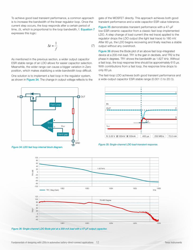
Figure 36 shows the Bode plot of an above fast loop-integrated device at a 200-mA load. TR1 is the gain in decibels, and TR2 is the phase in degrees. TR1 shows the bandwidth as 1.627 kHz. Without a fast loop, the loop response time should be approximately 615 µs. With contributions from a fast loop, the response time drops to only 60 µs.
The fast-loop LDO achieves both good transient performance and a wide-output capacitor ESR stable range (0.001 Ω to 20 Ω).
ft 1= (7)
Figure 34: LDO fast loop internal block diagram.Figure 35: Single-channel LDO load-transient response.
Figure 36: Single-channel LDO Bode plot at a 200-mA load with a 47-µF output capacitor.
GND
OUTIN
Fast Loop
+
–
Band gap
Error
AmpVREF
IN
1: 5.00 V 2:100mV 3:100mA
1
2
3
t
OUT
IOUT
400 µs 250 MS/s 70.0 mA
1.627kHz
78.485 Degree
10E2 10E3 10E4 10E5 10E6
100
-100
80
-80
60
-60
TR1: Mag (Gain) f/Hz
40
-40
20
-20
0
TR1/
dB
10E2 10E3 10E4 10E5 10E6
120
100
80
-40
TR2: Unwrapped Phase (Gain) f/Hz
40
-20
60
0
20TR2/
o

13 Fundamentals of designing with LDOs in automotive battery-direct-connect applications Texas Instruments
Junction temperature and thermal considerationsMost LDOs specify a maximum junction temperature to ensure a normal working condition. Exceeding this limit can potentially influence regulator reliability. This limit also constrains the regulator’s power dissipation. To ensure that the junction temperature is within an acceptable range, power dissipation must be lower than the maximum allowed, calculated using Equation 8:
where TJ_MAX is the maximum allowed junction temperature, TA is the ambient temperature and θJA is the ambient-to-junction thermal resistance specified in the data sheet.
For a TI standard data sheet, the θJA value is usually simulated using a JEDEC Solid State Technology Organization JESD51 2s2p PCB. Figure 37 shows the JESD51 2s2p PCB layer.
Let us assume that Table 4 shows thermal resistance of an LDO chip.
If the application condition is TA = 85°C, you can then calculate the maximum power dissipation using Equation 9 with the SOT-223 package as an example:
Using a JESD51 2s2p board, the power dissipation of this LDO needs to be less than 1.01 W to make sure that its junction temperature is lower than 150°C
Figure 38 shows an LDO with complete generic functions including enable, power good, adjustable output voltage, early warning, and watchdog timers.
JA
AJ TTP = max_
max
WTT
PJA
AJ 01.12.6485150max_
max ===
(8)
(9)
Figure 37: Cross-section of a JEDEC JESD51 2s2p board.
Table 4: Example of LDO thermal resistance.
Figure 38: Generic LDO application schematic.
70 µm Cu
1.5
mm
70 µm Cu
35 µm Cu
35 µm Cu
Thermal Resitance DCY(4P) DBV(5P) UNIT
RJA Junction to Ambient 64.2 210.4
38.4 oC/W
126.1
13.3
46.8
RJB Junction to Board
RJC Junction to Case(top)
IN OUTVDD
RESET
I/O
I/O
I/O
FB
PG
WDO
WD
PGADJ
SO
ENe.g.Ignition
SI
GNDGND
DELAY
Regulator OutputVoltage
ThermalShutdown
ThermalShutdown
ThermalShutdown
+
–
+
–
Reset and watchdog generator
Load MCU
VSAT

Thermal ranking by package
Figure 39 provides the thermal ranking for each package of available battery-direct-connect LDOs.
TI has a complete automotive battery-direct-connect LDO portfolio (see the product tree in Figure 40). LDOs in this product tree are classified by output current, quiescent current and functions.
Some TI automotive battery-direct-connect LDOs are designed for specific applications. For example, tracking the LDO, TPS7B425x-Q1, is used for automotive off-board sensor power supplies. The antenna LDO, TPS7B770x-Q1, is used for automotive antenna power supplies. Watchdog timers, LDO TPS7A63xx-Q1 and TPS7B68xx-Q1, are used for systems requiring higher reliability. Table 5 shows the targeted applications for these specific LDOs.
ConclusionBeing fully knowledgeable about the basic and advanced features of battery-direct-connect LDOs is essential to building a successful design. Understanding the technical background and meaning of a detailed specification can help you select the right LDO parts for your system.
Texas Instruments offers a complete portfolio of battery-direct-connect LDOs for automotive systems. By accessing this portfolio, you can quickly select an LDO based on the features and parameter preferences for your specific design
References
• LDO Parallel Solution Reference Design with TPS7B4253-Q1, TI Design (TIDUB16A), January 2016.
• Anda Zhang. How to choose TPS7B67xx-Q1 output capacitor, TI Application Report (SLVA759), December 2015.
• Jason Liu. Various Applications for Voltage-Tracking LDO, TI Application Report (SLVA789), August 2016.
• Learn more about LDOs from TI
Products
• TPS7B6701-Q1• TPS7B6750-Q1• TLE4275-Q1
Figure 39: TI automotive package thermal ranking.
SOT23
QFN
SOT223
DPAK
SOIC
MSOP
HTSSOP
DDPAK
Figure 40: TI automotive battery-direct-connect LDO selection guide.
> 200mA
TPS7A16xx-Q1(PG,E,F)TPS7B69xx-Q1TPS7A66xx-Q1(PG,E,F)TPS7A69xx-Q1(PG,EW)
TPS798xx-Q1(E,F) TPS7B67xx-Q1 TPS7A60xx-Q1(PG)TPS7A61xx-Q1(PG, E)TPS7A62xx-Q1(F, E)TPS7A63xx-Q1(PG, E, F, W)TPS7B63xx-Q1(PG, E, F, W)TPS7A64xx-Q1(PG, E, F, W)TPS7A65xx-Q1TPS7B68xx-Q1(PG, E, F, W)
TLE4275-Q1(PG, E)TL720M05-Q1
< 200mAOutput Current Range
Quiescent Current
< 25uA < 25uA < 50uA > 50uA> 25uA
Quiescent Current
Table 5: Application-specific LDO selection guide.
SENSOR
TPS7B4250-Q1TPS7B4253-Q1TPS7B4254-Q1
SAFETY FUNC
TPS7B68xx-Q1TPS7A63xx-Q1TPS7B63xx-Q1
ANTENNA
TPS7B7701-Q1TPS7B7702-Q1
© 2017 Texas Instruments Incorporated SLYB232The platform bar is a trademark of Texas Instruments. All other trademarks are the property of their respective owners.
Important Notice: The products and services of Texas Instruments Incorporated and its subsidiaries described herein are sold subject to TI’s standard terms and conditions of sale. Customers are advised to obtain the most current and complete information about TI products and services before placing orders. TI assumes no liability for applications assistance, customer’s applications or product designs, software performance, or infringement of patents. The publication of information regarding any other company’s products or services does not constitute TI’s approval, warranty or endorsement thereof.

IMPORTANT NOTICE FOR TI DESIGN INFORMATION AND RESOURCES
Texas Instruments Incorporated (‘TI”) technical, application or other design advice, services or information, including, but not limited to,reference designs and materials relating to evaluation modules, (collectively, “TI Resources”) are intended to assist designers who aredeveloping applications that incorporate TI products; by downloading, accessing or using any particular TI Resource in any way, you(individually or, if you are acting on behalf of a company, your company) agree to use it solely for this purpose and subject to the terms ofthis Notice.TI’s provision of TI Resources does not expand or otherwise alter TI’s applicable published warranties or warranty disclaimers for TIproducts, and no additional obligations or liabilities arise from TI providing such TI Resources. TI reserves the right to make corrections,enhancements, improvements and other changes to its TI Resources.You understand and agree that you remain responsible for using your independent analysis, evaluation and judgment in designing yourapplications and that you have full and exclusive responsibility to assure the safety of your applications and compliance of your applications(and of all TI products used in or for your applications) with all applicable regulations, laws and other applicable requirements. Yourepresent that, with respect to your applications, you have all the necessary expertise to create and implement safeguards that (1)anticipate dangerous consequences of failures, (2) monitor failures and their consequences, and (3) lessen the likelihood of failures thatmight cause harm and take appropriate actions. You agree that prior to using or distributing any applications that include TI products, youwill thoroughly test such applications and the functionality of such TI products as used in such applications. TI has not conducted anytesting other than that specifically described in the published documentation for a particular TI Resource.You are authorized to use, copy and modify any individual TI Resource only in connection with the development of applications that includethe TI product(s) identified in such TI Resource. NO OTHER LICENSE, EXPRESS OR IMPLIED, BY ESTOPPEL OR OTHERWISE TOANY OTHER TI INTELLECTUAL PROPERTY RIGHT, AND NO LICENSE TO ANY TECHNOLOGY OR INTELLECTUAL PROPERTYRIGHT OF TI OR ANY THIRD PARTY IS GRANTED HEREIN, including but not limited to any patent right, copyright, mask work right, orother intellectual property right relating to any combination, machine, or process in which TI products or services are used. Informationregarding or referencing third-party products or services does not constitute a license to use such products or services, or a warranty orendorsement thereof. Use of TI Resources may require a license from a third party under the patents or other intellectual property of thethird party, or a license from TI under the patents or other intellectual property of TI.TI RESOURCES ARE PROVIDED “AS IS” AND WITH ALL FAULTS. TI DISCLAIMS ALL OTHER WARRANTIES ORREPRESENTATIONS, EXPRESS OR IMPLIED, REGARDING TI RESOURCES OR USE THEREOF, INCLUDING BUT NOT LIMITED TOACCURACY OR COMPLETENESS, TITLE, ANY EPIDEMIC FAILURE WARRANTY AND ANY IMPLIED WARRANTIES OFMERCHANTABILITY, FITNESS FOR A PARTICULAR PURPOSE, AND NON-INFRINGEMENT OF ANY THIRD PARTY INTELLECTUALPROPERTY RIGHTS.TI SHALL NOT BE LIABLE FOR AND SHALL NOT DEFEND OR INDEMNIFY YOU AGAINST ANY CLAIM, INCLUDING BUT NOTLIMITED TO ANY INFRINGEMENT CLAIM THAT RELATES TO OR IS BASED ON ANY COMBINATION OF PRODUCTS EVEN IFDESCRIBED IN TI RESOURCES OR OTHERWISE. IN NO EVENT SHALL TI BE LIABLE FOR ANY ACTUAL, DIRECT, SPECIAL,COLLATERAL, INDIRECT, PUNITIVE, INCIDENTAL, CONSEQUENTIAL OR EXEMPLARY DAMAGES IN CONNECTION WITH ORARISING OUT OF TI RESOURCES OR USE THEREOF, AND REGARDLESS OF WHETHER TI HAS BEEN ADVISED OF THEPOSSIBILITY OF SUCH DAMAGES.You agree to fully indemnify TI and its representatives against any damages, costs, losses, and/or liabilities arising out of your non-compliance with the terms and provisions of this Notice.This Notice applies to TI Resources. Additional terms apply to the use and purchase of certain types of materials, TI products and services.These include; without limitation, TI’s standard terms for semiconductor products http://www.ti.com/sc/docs/stdterms.htm), evaluationmodules, and samples (http://www.ti.com/sc/docs/sampterms.htm).
Mailing Address: Texas Instruments, Post Office Box 655303, Dallas, Texas 75265Copyright © 2017, Texas Instruments Incorporated