future generation architectures and circuits for …
TRANSCRIPT

FUTURE GENERATION ARCHITECTURES AND CIRCUITS FOR
HIGH-SPEED I/O LINKS
A DISSERTATION
SUBMITTED TO THE FACULTY OF THE GRADUATE SCHOOL
OF THE UNIVERSITY OF MINNESOTA
BY
MAHMOUD REZA AHMADI
IN PARTIAL FULFILLMENT OF THE REQUIREMENTS
FOR THE DEGREE OF
DOCTOR OF PHILOSOPHY
June 2010

c© Mahmoud Reza Ahmadi 2010

Acknowledgments
During the course of my Ph.D. program at University of Minnesota, I was quite honored
with an extensive support and accompaniments of many extraordinary people. I have
had the opportunity to closely work, learn, gain required skills and live everyday with
these brilliant people who made this journey a signature chapter of my life. First of all,
I would like to express my deepest gratitude to Professor Ramesh Harjani, who has had
a significant impact on my career since my arrival to the Twin-Cites and starting my
research program in Analog Design Group under his supervision. His continuous and
comprehensive support, positive attitude, brilliant line of thoughts and powerful problem
solving abilities taught me how to broaden my view for exploring and conducting research
topics. I would like to take this opportunity to thank my co-adviser, Professor Jaekyun
Moon, who instructed and guided my research thesis in advanced digital communication
and my respected committee members, Professors Anand Gopinath, Ofer Zeitouni and
Chris Kim for their time to review of this thesis.
During my internship programs at Rambus Inc. and Qualcomm Inc., I was acquainted
and worked closely with an excellent group of technology professionals in the Bay Area,
California. I am highly indebted to Amir Amirkhany, my close friend and mentor, who
widened my research scope to a new sets of problems and has significantly contributed
to a major section of my research thesis. I appreciate Jafar Savoj who generously spent
time and guided me in analyzing and solving several research problems and Ali-Azam
Abbasfar, Bruno Garlepp, Haechang Lee and Farid Assaderaghi for the time and in-depth
i

technical discussions.
Minneapolis and its historically-known friendly people has been by the far the best
city where I lived since leaving my native city, Tehran. Not only people from my research
lab are among the bests in their work, but also they established a rarely found friendship
circle which will be the foundation of many future cooperation. I am grateful of Kin-
Joe Sham who helped extensively with tape-out deadlines through his capability to go
sleepless for days, Shubha Bommalingaiahnapallya, Satwik Patnaik, Narasimha Lanka
for the support, great technical discussions and lab measurement help and Josh Wibben,
Yihung Tseng, Taehyoun Oh, Bodhi Sadhu and Jaehyup Kim for help and support. Over
the past fifteen years, my closest friends Shahrouz Takyar’s and Ali Enteshari’s continual
support and kindness have been a spirit booster.
I am thankful of my soul-mate Meggan’s generosity who has been supportive of
my work and persistently encouraging fulfilment of various stages. Lastly what defies
any description in any language is my acknowledgement to my magnanimous family
members whose perpetual love and passion makes me greatly humbled and honored.
Most specifically, my sisters, Fahimeh and Fariba have been extremely dedicated and
supportive of me in every single step. My brother-in-laws Hamid and Bahman have
been there for me all the time. Omid provided a lot of fun times since he showed up
in Minneapolis, Negar and Farnoush have been sweet and kind and my parents, Farideh
and Mohammad, without whom everlasting support and sacrifices, none of these would
have been possible.
ii
Abstract
The persistent demand for increased data throughput in computer desktops and
servers has been driving the design and development of high-speed I/O links in CMOS
technologies. Frequency dependent channel loss and imperfections, such as impedance
discontinuities, in I/O transceiver building blocks lead to inter-symbol interference (ISI)
which limits the achievable link throughput. Crosstalk noise from neighboring channels
results in both timing and amplitude errors with the growing data rate trends in chip-to-
chip communication. In addition, increasing ISI and crosstalk noise sources complicates
the design of critical circuit blocks such as timing recovery. All these factors exacerbate
the eye closure at the receiver and adversely affect the performance or bit-error-rate
(BER) of the overall link. This thesis extends the design scope of current high-speed
I/O systems by applying the joint know-how in advanced digital communication and
novel circuit implementations. Several architectures and schemes including equalization,
timing recovery and timing generation circuits are proposed which address some of the
limiting factors in today’s chip-to-chip I/O links.
First, partial response (PR) equalization is presented, analyzed and demonstrated
as a successful candidate for steep roll-off channel classes. Based on this technique, a
transceiver with PR transmit equalizer and a 1-tap decision feedback equalizer (DFE) is
proposed which increases the signal to noise (SNR) of the received signal at the receiver
decision circuit input. The proposed PR1.1.b equalization in this thesis outperforms
duobinary signaling by 28% and 19% when comparing vertical eye opening and by 10%
iii

and 7% when comparing horizontal eye opening at 10Gbps and 15Gbps respectively.
These improvements become significantly higher when the channel is subjected to severe
crosstalk noise sources. Additionally this architecture mitigates the circuit design issue
related to tight DFE loop timing and convergence.
Second, a novel pilot-based clock and data recovery (CDR) circuit is introduced that
eliminates the clock recovery performance dependency on channel ISI components. A
5Gbps CDR prototype was designed and fabricated in a 0.13μm CMOS technology which
uses simultaneously data and clock transmission over the same channel. The measured
recovered clock rms jitter was 1.6ps while only a 5% voltage overhead was imposed onto
the transmitter for the pilot signal when subjected to a channel loss of 10dB.
Third, a 5.6GHz transmit phase-locked-loop (PLL), prototyped in a 0.18μm CMOS
technology, is also presented which dynamically corrects the charge-pump (CP) current
and reduces the side-band spurs by 22dB and therefore improves the jitter quality of
the PLL generated clock.
Finally a unified configurable I/O transceiver solution is introduced that takes ad-
vantages of all the architecture schemes and circuits proposed throughout the thesis for
future chip-to-chip communication ICs.
iv

Contents
List of Figures viii
List of Tables xiii
1 Introduction 1
1.1 Broadband Chip-to-Chip Communication . . . . . . . . . . . . . . . . . . 1
1.2 High-Speed Link Schemes . . . . . . . . . . . . . . . . . . . . . . . . . . . 3
1.3 Thesis Organization . . . . . . . . . . . . . . . . . . . . . . . . . . . . . . 5
2 Background 8
2.1 Signal Integrity Basics . . . . . . . . . . . . . . . . . . . . . . . . . . . . . 8
2.2 Channel Model . . . . . . . . . . . . . . . . . . . . . . . . . . . . . . . . . 9
2.3 Inter-Symbol-Interference (ISI) . . . . . . . . . . . . . . . . . . . . . . . . 11
2.4 Crosstalk Noise . . . . . . . . . . . . . . . . . . . . . . . . . . . . . . . . . 12
2.5 Timing Noise (Jitter) . . . . . . . . . . . . . . . . . . . . . . . . . . . . . . 14
2.6 System Performance Analysis . . . . . . . . . . . . . . . . . . . . . . . . . 16
v
2.7 Equalization . . . . . . . . . . . . . . . . . . . . . . . . . . . . . . . . . . . 18
2.8 Reference Clock Generation . . . . . . . . . . . . . . . . . . . . . . . . . . 23
2.9 Timing Recovery . . . . . . . . . . . . . . . . . . . . . . . . . . . . . . . . 23
3 Constrained Partial Response Equalizers for High-Speed Links 28
3.1 Generalized Partial Response Equalizers . . . . . . . . . . . . . . . . . . . 30
3.2 Crosstalk in Partial Response Equalization . . . . . . . . . . . . . . . . . 34
3.3 Novel Architecture for Memory Channels . . . . . . . . . . . . . . . . . . 36
3.4 MMSE Optimization Problem . . . . . . . . . . . . . . . . . . . . . . . . . 39
3.5 Performance Comparison of PR Equalizers . . . . . . . . . . . . . . . . . . 42
3.6 Performance Comparison of PR Equalization with Crosstalk Noise . . . . 47
3.7 Summary . . . . . . . . . . . . . . . . . . . . . . . . . . . . . . . . . . . . 49
4 Pilot-Based CDR Scheme for High-Speed Links 51
4.1 The Proposed Architecture . . . . . . . . . . . . . . . . . . . . . . . . . . 54
4.2 System Level Analysis and Tradeoffs . . . . . . . . . . . . . . . . . . . . . 56
4.2.1 System Level Simulation . . . . . . . . . . . . . . . . . . . . . . . . 59
4.3 Prototype Circuit Design . . . . . . . . . . . . . . . . . . . . . . . . . . . 60
4.3.1 LC-Tuned Amplifier . . . . . . . . . . . . . . . . . . . . . . . . . . 63
4.3.2 Injection Locked Oscillator . . . . . . . . . . . . . . . . . . . . . . 64
4.3.3 Source Degeneration Amplifier and Analog Equalizer . . . . . . . . 66
4.3.4 CML D-Flip-Flop . . . . . . . . . . . . . . . . . . . . . . . . . . . 67
4.3.5 Phase Adjustment . . . . . . . . . . . . . . . . . . . . . . . . . . . 69
vi

4.3.6 Transmitter with Power Combined Pilot and NRZ Data . . . . . . 70
4.4 Experimental Results . . . . . . . . . . . . . . . . . . . . . . . . . . . . . . 71
4.5 Summary . . . . . . . . . . . . . . . . . . . . . . . . . . . . . . . . . . . . 78
5 Low Spur Single-Ended Charge-Pump PLL 81
5.1 Spur Generation in Single-Ended PLLs . . . . . . . . . . . . . . . . . . . . 83
5.2 Proposed Reduced Spur Charge-Pump Circuit . . . . . . . . . . . . . . . . 87
5.3 Phase Noise Analysis . . . . . . . . . . . . . . . . . . . . . . . . . . . . . . 89
5.4 Prototype Circuit Design . . . . . . . . . . . . . . . . . . . . . . . . . . . 90
5.5 Experimental Results . . . . . . . . . . . . . . . . . . . . . . . . . . . . . . 94
5.6 Summary . . . . . . . . . . . . . . . . . . . . . . . . . . . . . . . . . . . . 100
6 Conclusions, Research Contribution & Future Directions 101
6.1 Future Directions . . . . . . . . . . . . . . . . . . . . . . . . . . . . . . . . 103
6.1.1 Adaptive Phase Recovery for Pilot-Based CDR Scheme . . . . . . 103
6.1.2 A Unified Pilot-Based CDR and PR Equalization I/O Transceiver 104
A Partial Response MMSE Optimization Problem 106
Bibliography 115
vii

List of Figures
1.1 I/O and processor technology roadmap . . . . . . . . . . . . . . . . . . . . 2
1.2 HyperTransport and PCI-Express examples illustrating high-performance
interconnection for processor-processor and processor-graphic cores . . . . 3
1.3 Embedded clock I/O. Clock and data are transmitted over the same channel 4
1.4 Source synchronous I/O. Clock and data are transmitted in two different
channels . . . . . . . . . . . . . . . . . . . . . . . . . . . . . . . . . . . . . 5
2.1 High-speed link building blocks for chip-chip communication applications 9
2.2 Typical transmit data bits and the distorted received signal due to limited
bandwidth . . . . . . . . . . . . . . . . . . . . . . . . . . . . . . . . . . . . 9
2.3 Channel frequency response and loss mechanisms with and without dis-
continuity and simple equivalent transmission line model . . . . . . . . . . 10
2.4 FEXT time domain response for a victim line with two aggressors . . . . 13
2.5 NEXT time domain response for a victim line with two aggressors . . . . 14
2.6 Total jitter relation with random and deterministic jitter PDF . . . . . . 15
viii

2.7 2-PAM simplified eye diagram with voltage and time error decision thresh-
olds . . . . . . . . . . . . . . . . . . . . . . . . . . . . . . . . . . . . . . . 17
2.8 Simulated and a sample measured eye diagrams for bandwidth limited
channels . . . . . . . . . . . . . . . . . . . . . . . . . . . . . . . . . . . . . 18
2.9 Equalizer techniques used in a today’s typical high-speed links . . . . . . 20
2.10 Frequency and time domain responses of various equalizer techniques . . . 21
2.11 Simplified closed-loop timing recovery circuit using an edge-based CDR . 24
2.12 DLL based phase alignment circuit for per data channel timing recovery . 26
3.1 Generalized and constrained partial response equalization technique . . . 31
3.2 Measured stripline and microstripline channel pulse responses . . . . . . . 32
3.3 (a) General impulse response at T1−Symb and (b) at T2−Symb . . . . . . . 33
3.4 Frequency response of different target PR equalizers . . . . . . . . . . . . 35
3.5 Stripline and microstrip channel responses . . . . . . . . . . . . . . . . . . 36
3.6 Microstrip symbol rate pulse response at 10Gb/s . . . . . . . . . . . . . . 37
3.7 System link architecture for a PR target of [1 1 bopt] . . . . . . . . . . . . 39
3.8 Jmin variation vs. number of TX equalization taps and different PRs . . . 42
3.9 PR equalizer eye diagram at 10Gb/s, (a)PR1(b)PR1.1(c)PR1.1.b with bopt
= 0.0515 . . . . . . . . . . . . . . . . . . . . . . . . . . . . . . . . . . . . . 43
3.10 PR equalizer eye diagram at 15Gb/s, (a)PR1(b)PR1.1(c)PR1.1.b with bopt
= 0.0613 . . . . . . . . . . . . . . . . . . . . . . . . . . . . . . . . . . . . . 44
3.11 Variation of optimized bopt versus data rate for the channel in Figure 3.4 . 45
ix

3.12 Impact of crosstalk noises on PR1.1 transmit equalization (a) Eliminating
crosstalk noises from MMSE problem (b) Including crosstalk noises in
MMSE problem . . . . . . . . . . . . . . . . . . . . . . . . . . . . . . . . . 48
3.13 Impact of crosstalk noises on PR1.1.b transmit equalization (a) Eliminating
crosstalk noises from MMSE problem (b) Including crosstalk noises in
MMSE problem . . . . . . . . . . . . . . . . . . . . . . . . . . . . . . . . . 49
4.1 The proposed architecture using a pilot-based CDR with pilot frequency
equal to bitrate . . . . . . . . . . . . . . . . . . . . . . . . . . . . . . . . . 54
4.2 Frequency Spectrum of Aggregated NRZ data and pilot . . . . . . . . . . 57
4.3 Mixer base PLL receiver (a) Mathematical model presented by Viterbi
(b) [1] . . . . . . . . . . . . . . . . . . . . . . . . . . . . . . . . . . . . . . 58
4.4 The proposed 5Gb/s prototype receiver using an injection locked oscillator 63
4.5 Differential LC-tuned amplifier . . . . . . . . . . . . . . . . . . . . . . . . 64
4.6 Injection locked based oscillator . . . . . . . . . . . . . . . . . . . . . . . . 65
4.7 Source degeneration and analog equalizer . . . . . . . . . . . . . . . . . . 67
4.8 CML latch used in a master-slave D-flip-flop . . . . . . . . . . . . . . . . . 68
4.9 On-chip combination of data and pilot at the transmitter . . . . . . . . . 70
4.10 Off-chip combination of data and pilot at the transmitter with phase ad-
justment . . . . . . . . . . . . . . . . . . . . . . . . . . . . . . . . . . . . . 71
4.11 Chip Micrograph, The receiver area is 0.2914mm2 including all the buffers
and pad drivers and the CDR occupies 0.171mm2 . . . . . . . . . . . . . . 73
x

4.12 Designed test board using open cavity QFN5x5 32A and probing the input
combined data and pilot and recovered clock and data . . . . . . . . . . . 74
4.13 Recovered clock for pilot to data overhead of 5% and FR4 length of 5” . . 75
4.14 Eye diagram after power splitters and without FR4 channel (a) recovered
clock and data, data transition uncertainties improvement of about 50%(b) 76
4.15 Received eye diagram after power splitters and a 10” FR4 channel (a)
recovered clock and data, data transition uncertainties improvement of
58%(b) . . . . . . . . . . . . . . . . . . . . . . . . . . . . . . . . . . . . . . 77
4.16 Pilot-based CDR bandwidth variation versus received pilot amplitude for
a fixed transmitted data amplitude . . . . . . . . . . . . . . . . . . . . . . 78
4.17 Transmit pilot rms jitter before the channel and recovered clock rms jitter
versus the received pilot amplitude for a fixed transmitted data amplitude 79
5.1 Traditional PFD used in charge-pump PLL. Td or duration of correction
pulses generated in traditional PFD . . . . . . . . . . . . . . . . . . . . . 84
5.2 Charge-pump currents in PFD based PLL . . . . . . . . . . . . . . . . . . 86
5.3 Simplified proposed charge-pump circuit in lock condition . . . . . . . . . 88
5.4 IUp and IDown current mismatches in the lock condition. a) conventional
charge-pump b) proposed charge-pump . . . . . . . . . . . . . . . . . . . . 89
5.5 Op-amp noise, equivalent noise and noise spectrum at VCO input . . . . . 91
5.6 Op-amp circuit in the proposed charge-pump . . . . . . . . . . . . . . . . 91
5.7 Conventional control line transient behavior . . . . . . . . . . . . . . . . . 92
xi

5.8 Proposed design control line transient behavior (3.5X reduction) . . . . . 93
5.9 Measured transient response and output spectrum for the proposed design
in lock. tsettling=2.2μs, flock= 5.76GHz . . . . . . . . . . . . . . . . . . . . 95
5.10 Spur level comparison of the two designs over the lock range. Peak im-
provement > 22dB . . . . . . . . . . . . . . . . . . . . . . . . . . . . . . . 96
5.11 Measured output spectrum of conventional design (a) and proposed de-
signs (b) at fRef = 118 MHz . . . . . . . . . . . . . . . . . . . . . . . . . . 97
5.12 Microphotograph of the PLLs in a 0.18μm CMOS technology. . . . . . . . 98
5.13 ITRS supply voltage roadmap for CMOS . . . . . . . . . . . . . . . . . . 98
6.1 Proposed phase adjustment with eye height monitoring and interpolators 103
6.2 Unified pilot-based CDR and PR equalization scheme for I/O transceivers 105
xii

List of Tables
3.1 Crosstalk FOM for different PR equalization targets for the channel model
with 30” length and 20mil spacings [2] . . . . . . . . . . . . . . . . . . . . 36
3.2 Performance summary for 12” microstrip with connectors . . . . . . . . . 47
4.1 System Level Simulation of Pilot Based CDR for the Cases Illustrated in
Figure 4.2 . . . . . . . . . . . . . . . . . . . . . . . . . . . . . . . . . . . . 61
4.2 Performance comparison with recently reported CDRs . . . . . . . . . . . 80
5.1 Summary of measurement results . . . . . . . . . . . . . . . . . . . . . . . 99
5.2 Performance comparison of PLLs with improved charge-pump Circuits . . 100
xiii

Chapter 1
Introduction
1.1 Broadband Chip-to-Chip Communication
The emergence of digital data communications has created a distinct turning point in
the history of communication technology by eliminating some limitations in analog voice
and data transmission. Digital communications provide a compatible domain for inter-
connection of various digital systems. Perhaps telegraphy and teletypewriters are the
predecessors to most of today’s digital communication systems where the information
is transmitted in digital domain in both systems. Following the basic development of
digital communication theory, various applications appeared through the years using
data processing and transmission. With the advent of large scale integrated circuits
(IC) in 1960 followed by the internet in 1969, the need for higher data throughput and
bandwidth has substantially increased. The development of IC technologies provided the
realization possibilities for higher frequency ICs but at increased manufacturing costs.
1
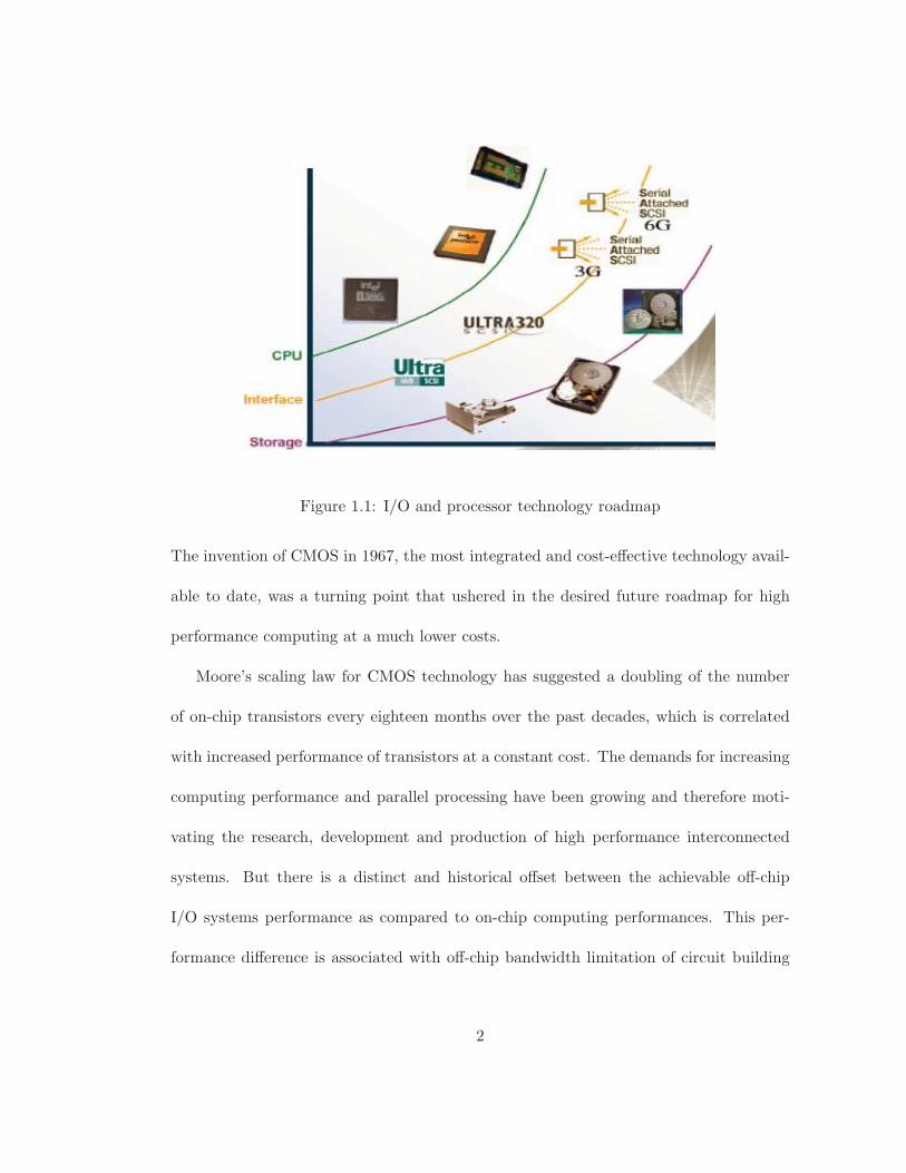
Figure 1.1: I/O and processor technology roadmap
The invention of CMOS in 1967, the most integrated and cost-effective technology avail-
able to date, was a turning point that ushered in the desired future roadmap for high
performance computing at a much lower costs.
Moore’s scaling law for CMOS technology has suggested a doubling of the number
of on-chip transistors every eighteen months over the past decades, which is correlated
with increased performance of transistors at a constant cost. The demands for increasing
computing performance and parallel processing have been growing and therefore moti-
vating the research, development and production of high performance interconnected
systems. But there is a distinct and historical offset between the achievable off-chip
I/O systems performance as compared to on-chip computing performances. This per-
formance difference is associated with off-chip bandwidth limitation of circuit building
2

Figure 1.2: HyperTransport and PCI-Express examples illustrating high-performance
interconnection for processor-processor and processor-graphic cores
blocks. The illustrated gap in Figure 1.1 has been the major motivation behind the
enhancement of more sophisticated I/O links both in academic and industrial research
and production. I/O systems have a wide range of applications such as servers, desktops,
internet links, gaming consoles and sophisticated graphic chips. A familiar example can
be found inside today’s PCs, where high-speed links are used to interconnect multi-core
processors, processors to memory and processors to graphic processors. Figure 1.2 shows
a current example of “AMD” high-performance platform including high-speed links, such
as “HyperTransport” and “PCI-Express”, to interconnect processor cores and processors
to graphic cards.
1.2 High-Speed Link Schemes
A high-speed link is a synchronous system which is composed of a transmitter, a medium
channel which carries the signal and a receiver block. Clock information is extracted at
receivers and the recovered clock is used to re-sample the incoming data for further
3
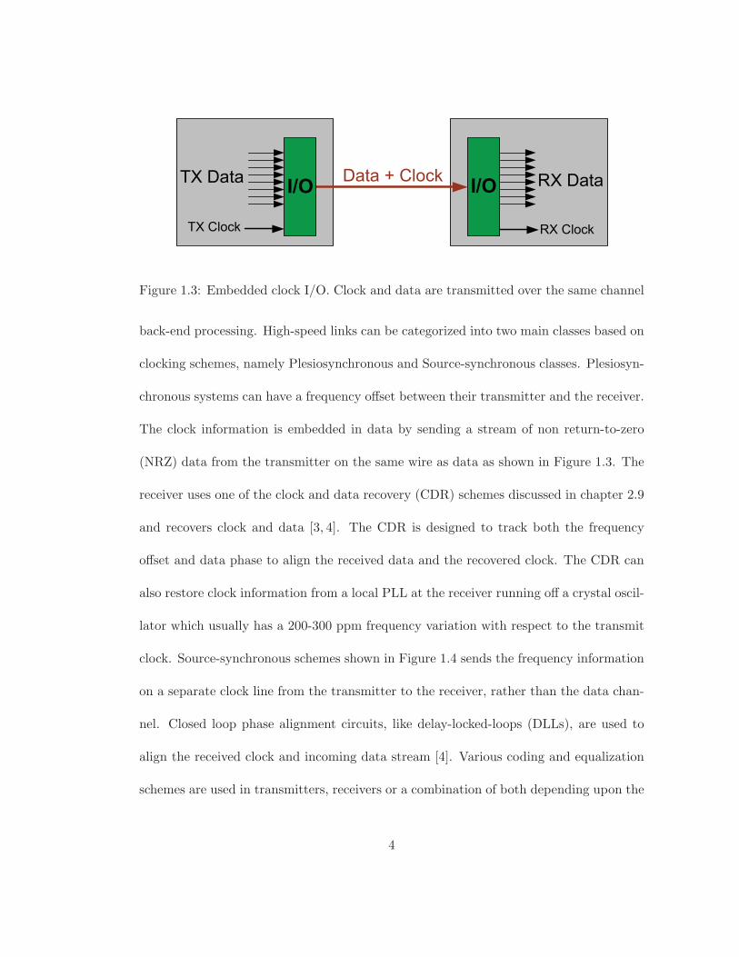
Figure 1.3: Embedded clock I/O. Clock and data are transmitted over the same channel
back-end processing. High-speed links can be categorized into two main classes based on
clocking schemes, namely Plesiosynchronous and Source-synchronous classes. Plesiosyn-
chronous systems can have a frequency offset between their transmitter and the receiver.
The clock information is embedded in data by sending a stream of non return-to-zero
(NRZ) data from the transmitter on the same wire as data as shown in Figure 1.3. The
receiver uses one of the clock and data recovery (CDR) schemes discussed in chapter 2.9
and recovers clock and data [3, 4]. The CDR is designed to track both the frequency
offset and data phase to align the received data and the recovered clock. The CDR can
also restore clock information from a local PLL at the receiver running off a crystal oscil-
lator which usually has a 200-300 ppm frequency variation with respect to the transmit
clock. Source-synchronous schemes shown in Figure 1.4 sends the frequency information
on a separate clock line from the transmitter to the receiver, rather than the data chan-
nel. Closed loop phase alignment circuits, like delay-locked-loops (DLLs), are used to
align the received clock and incoming data stream [4]. Various coding and equalization
schemes are used in transmitters, receivers or a combination of both depending upon the
4

Figure 1.4: Source synchronous I/O. Clock and data are transmitted in two different
channels
signal quality requirements, as will be discussed in the next chapter.
1.3 Thesis Organization
Due to system and circuit non-idealities, it is quite challenging to achieve the projected
off-chip I/O bandwidth indicated by International Technology Roadmap for Semiconduc-
tors (ITRS) as will be discussed later in chapter 2 [5]. Digital communication techniques
such as equalization and coding are used widely in high-speed links to overcome these
limitations. This thesis presents several architectures and circuit techniques which im-
prove the performance of current I/O systems for future generation chip-chip I/O systems
at increased data rates.
Chapter 2 gives an introduction to traditional high-speed link architectures and some
critical building blocks. This chapters also explains some major circuit and architecture
limiting issues in current I/O systems with increased data rates.
Chapter 3 proposes a novel architecture and theoretical analysis based on partial
5

response equalization to optimize the signaling and equalization which can be applied
to majority of today’s chip-chip I/O applications. In this scheme, the signaling band-
width is reduced and therefore the system performance was improved significantly by
incorporating the crosstalk noise into the link optimization problem. The architecture
will be shown to improve the design limitations existing in traditional nonlinear receiver
equalization techniques.
Clock and data recovery circuits and their interaction with other I/O building blocks
is one of the most tedious problems in chip-chip communication. The current issues
become more pronounced with the solid trend in growing data throughput and therefore
the bandwidth of I/O systems. Many of these circuits use a traditional edge-based
CDR loops for embedded clock schemes where their output performance are sensitive
to incoming data patterns. Chapter 4 presents a pilot-based CDR scheme along with a
low power circuit solution which decouples the timing recovery loop performance from
incoming data pattern. This concept will be verified both at the system level by analysis
and simulation and at the circuit level by measured performance results of the designed
prototype chip in a 0.13μm CMOS technology.
As briefly described in Section 1.2, transmitter clock generation is of an extreme
importance in determining the overall performance of synchronous links as well as many
of today’s wireless systems-on-a-chip (SOCs). Transmitter clock generators, PLLs, which
are used to clock the output data stream onto the channel and the receiver, define the
quality of the recovered clock at the receiver in a given design. Reference side-band spurs
6

are one of the main factors which adversely impact the jitter quality of the generated
clock as well as the output phase noise. Chapter 5 introduces a novel low-spur single-
ended charge-pump (CP) PLL which uses a modified CP circuit to reduce the generated
reference spurs from the PLL. The design outperforms the previous published techniques
and is supported by the measurement results from the designed chip in a 0.18μm CMOS
technology.
Chapter 6 concludes the thesis with a summary of results from the previous chapters
and sets the stage and direction for future research to enhance the features of individual
designed blocks. This chapter also proposes an advanced configurable transceiver solu-
tion by applying a combination of techniques presented in the prior chapters for future
I/O links.
7
Chapter 2
Background
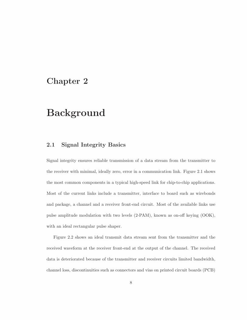
2.1 Signal Integrity Basics
Signal integrity ensures reliable transmission of a data stream from the transmitter to
the receiver with minimal, ideally zero, error in a communication link. Figure 2.1 shows
the most common components in a typical high-speed link for chip-to-chip applications.
Most of the current links include a transmitter, interface to board such as wirebonds
and package, a channel and a receiver front-end circuit. Most of the available links use
pulse amplitude modulation with two levels (2-PAM), known as on-off keying (OOK),
with an ideal rectangular pulse shaper.
Figure 2.2 shows an ideal transmit data stream sent from the transmitter and the
received waveform at the receiver front-end at the output of the channel. The received
data is deteriorated because of the transmitter and receiver circuits limited bandwidth,
channel loss, discontinuities such as connectors and vias on printed circuit boards (PCB)
8
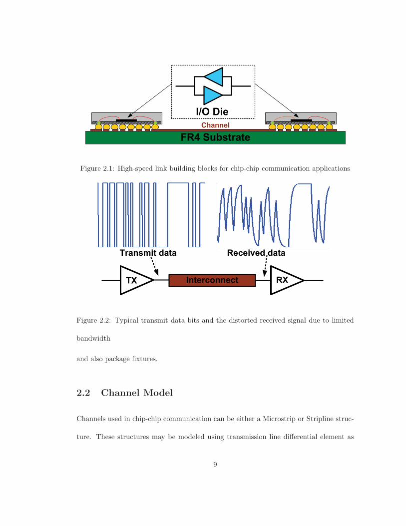
Figure 2.1: High-speed link building blocks for chip-chip communication applications
Figure 2.2: Typical transmit data bits and the distorted received signal due to limited
bandwidth
and also package fixtures.
2.2 Channel Model
Channels used in chip-chip communication can be either a Microstrip or Stripline struc-
ture. These structures may be modeled using transmission line differential element as
9

Figure 2.3: Channel frequency response and loss mechanisms with and without discon-
tinuity and simple equivalent transmission line model
shown in Figure 2.3 where “R” is the conductance loss per unit distance including skin
effect,“L” is the inductance per unit distance, “C” is the capacitance per unit distance
including the fringing capacitance and “G” is the dielectric loss. Frequency dependent
channel loss, which is the cause of the low-pass response behavior, is one of the major
non-ideality factors which limits the overall system throughput in high-speed links. Fig-
ure 2.3 shows the typical channel frequency responses observed in I/O applications with
and without connectors, risers and various discontinuities. The channel notches shown
in the figure are due to reflections from discontinuities such as connectors, risers and
package fixture.
FR4 is the cheapest and most attractive substrate material solution used by mother-
broad vendors in the PC, and server business where high-speed channels are routed in
10

chip-to-chip applications. Unfortunately FR4 board material has a poor quality (hence,
cheap) and is significantly lossy, low bandwidths, at high frequencies which results in ISI
and impedes the increasing demand for pushing the data rate for inter-chip communica-
tion. Skin effect and dielectric loss are the two major loss mechanisms associated with
channel loss. Skin effect loss is proportional to 1/√f while dielectric loss varies with 1/f
where f is the frequency of operation. This makes the skin effect a prominent factor at
lower frequencies while dielectric loss dominates at higher frequencies.
2.3 Inter-Symbol-Interference (ISI)
There are various flavors of ISI definition in both digital communication and circuit
design [6,7]. ISI is the interference of the previous transmitted symbols with the current
received symbol at the decision device, slicer, which affects both voltage and timing
margin of the received symbol and therefore the receiver decision. The major causes of
ISI are the limited channel bandwidth, transmitter and receiver circuits, and therefore
a finite memory in the system impulse response when evaluated at the symbol rate
intervals.
A general I/O system shown in Figure 2.1 can be simplified and analyzed using linear
time-invariant (LTI) system theory. The overall system impulse response, defined here
as h(t), is the convolution of transmitter impulse responses, channel and receiver circuits
impulse responses. The transmitter impulse response is defined as the convolution of
an ideal rectangular pulse, pulse shaper, and impulse response of transmitter circuits.
11

This relation has been shown in equation (2.1) where htx(t) is the transmitter impulse
response, hch(t) is the channel impulse response and hrx(t) is the receiver circuits im-
pulse response. The transmitter impulse response is normally dominated by the limited
bandwidth of final output driver stage while the receiver impulse response is usually
defined by the bandwidth of the front-end amplifier circuits.
In this equation, x(n) represents random 2-PAM data stream at the transmitter,
h(n) is overall system response and y(n) is the signal at discrete time indices of “n”. ISI
is the values of y(t) sampled at symbol period, and when evaluated at all discrete times
“l” when l �= n as in( 2.1). Timing recovery loops also impact the timing margin of the
received signal and in more complicated cases might even affect its voltage margin i.e.
when timing recovery is used with adaptive equalization [8, 9]. Later in this chapter we
will discuss the impact of timing recovery loops on the overall receiver performance.
h(t) = htx(t) ∗ hch(t) ∗ hrx(t)
y(n) = x(n) ∗ h(n) =∞∑
k=−∞h(kTs)x(n− k)
ISI = y(l) when l �= n (2.1)
2.4 Crosstalk Noise
Source-synchronous links such as HyperTransport have long and complicated PCB data
channel routings [10]. The production cost is highly impacted by channel routing area
which can be reduced substantially by smaller spacing, and the clearance between high-
12

Figure 2.4: FEXT time domain response for a victim line with two aggressors
speed lines. High-speed lines running adjacent to each other show the coupling effect
which is simply an induced signal from an aggressor line on the neighboring channel,
victim, as shown in Figures 2.4 and 2.5.
Figure 2.4 illustrates far-end crosstalk (FEXT) which is the coupling term at the
receiver induced by the aggressor transmit signal and after being attenuated by the
channel. Near-end crosstalk (NEXT) is caused by neighboring aggressor signals and
before channel attenuation in bi-directional links as depicted in Figure 2.5. NEXT can
severely impact the quality of received signals in hard drive applications i.e. SATA and
SAS standards [11]. As illustrated in Figures 2.4 and 2.5, the victim channel is turned
off in order to demonstrate crosstalk induced noise.
Crosstalk results from two major sources of interaction- capacitive and inductive,
which can occur in various system blocks like channel, connectors, package balls and
13

Figure 2.5: NEXT time domain response for a victim line with two aggressors
leads in multi-lane applications. Therefore crosstalk only impacts the received signal at
the transition points of the aggressor signal as it has a high-pass (derivative) nature.
Capacitive coupling causes the crosstalk components which are in phase with aggressor
signal while inductive coupling results in the crosstalk terms with 180 degree phase
shifted with respect to the aggressors [4]. Crosstalk from aggressors degrades both the
voltage and timing margin at the receiver sampler and the overall signal integrity.
2.5 Timing Noise (Jitter)
Clock, or timing reference is used to re-sample the received signal in all synchronous
schemes discussed in chapter 1.1. The period of the recovered clock (and therefore its
frequency) deviates from the nominal value of Ts due to various noise sources and band-
14

Figure 2.6: Total jitter relation with random and deterministic jitter PDF
width limitations. The threshold crossing point of the recovered clock has uncertainty
and deviates from the nominal point. This deviation is called timing noise or jitter and
is normally used by high-speed wireline community as a metric to evaluate the quality
of generated or recovered clock. Timing noise impacts the overall system performance as
will be explained in the next section. Jitter is the time domain translation of phase-noise
which is commonly used in the wireless system design jargon. More specifically, jitter
is the square root of integrated phase-noise within the receiver bandwidth when scaled
with the clock nominal frequency [3].
There are two major jitter components- random for example thermal noise and de-
terministic such as data-dependent. Random jitter is modeled by a Gaussian PDF which
is valid when the dominant noise in the system is thermal. Jitter can also result from
a random voltage noise at the crossing point of the signal which is inversely propor-
tional to the signal slope evaluated at the threshold crossings. Data dependent jitter
stems from the received signal threshold variation due to data pattern changes. This is
mostly because of limited bandwidth of the whole system [12]. Deterministic jitter is
normally modeled by non-Gaussian PDF or with a dual-dirac model [13]. As equations
(2.2) and Figure 2.6 demonstrate, the total jitter PDF is a convolution of random jitter
15

and deterministic jitter and total jitter variance is the summation of random jitter and
deterministic jitter variances assuming that the timing noise sources are uncorrelated.
It is worth noting that commonly used term of jitter rms, Jrms, is square root of the
total jitter variance and jitter peak to peak, Jp−p, is the maximum deviation of threshold
crossing point in the receiver recovered clock.
PDFTJ = PDFRJ ∗ PDFDDJ
σ2TJ = σ2
RJ + σ2DDJ (2.2)
2.6 System Performance Analysis
The performance of high-speed I/O systems are evaluated and measured by BER num-
bers for example 10−12, 10−15, etc., which actually represents the probability of detection
error, Pe, in these systems. Recalling from digital communication basics, Pe is defined
as in equation 2.3 in a 2-PAM constellation. Pe is either due to voltage or timing noise,
resulting in an erroneous decisions at the receiver and as depicted for both voltage and
time decision error in Figure 2.7 [14]. Assuming the random noise is the dominant noise
source which is modeled by a Gaussian PDF with variance of σ2n, BER of the system
can be defined as in equation (2.3) where y is the received signal and yth is the decision
threshold for 2-PAM signaling [6].
The analytical calculation of BER in equation (2.3) is a powerful tool and can be
used similarly for various constellations in digital communication. But it is practically
impossible to use this equation as an accurate evaluation of overall system performance
16

Figure 2.7: 2-PAM simplified eye diagram with voltage and time error decision thresholds
in real designs. It is quite complicated to model and apply the statistics of all noise
sources using the relation in equation (2.3). Therefore, I/O designers normally use eye
diagrams to characterize the system performance. BER analysis and measurement are
then performed as the last step in the system performance evaluation.
Pe = Pr(y(n) = 1 | x(n) = 0).P r(x(n) = 0) + Pr(y(n) = 0 | x(n) = 1).P r(x(n) = 1)
BER = Pe =1
2√
2σ2n
(∫ ∞
yth
e−(y−yth)2
2σ2n dy +
∫ yth
−∞e−(y−yth)2
2σ2n dy
)(2.3)
The eye diagram is created by overlapping a long stream of received signals when
sliced at the time intervals equal to reciprocal of the transmit symbol rate. Figure 2.8(a)
shows a simulated eye diagram for a typical link model with received signal shown in
Figure 2.2 while Figure 2.8(b) depicts the sampled eye diagram for a 5Gb/s received
17
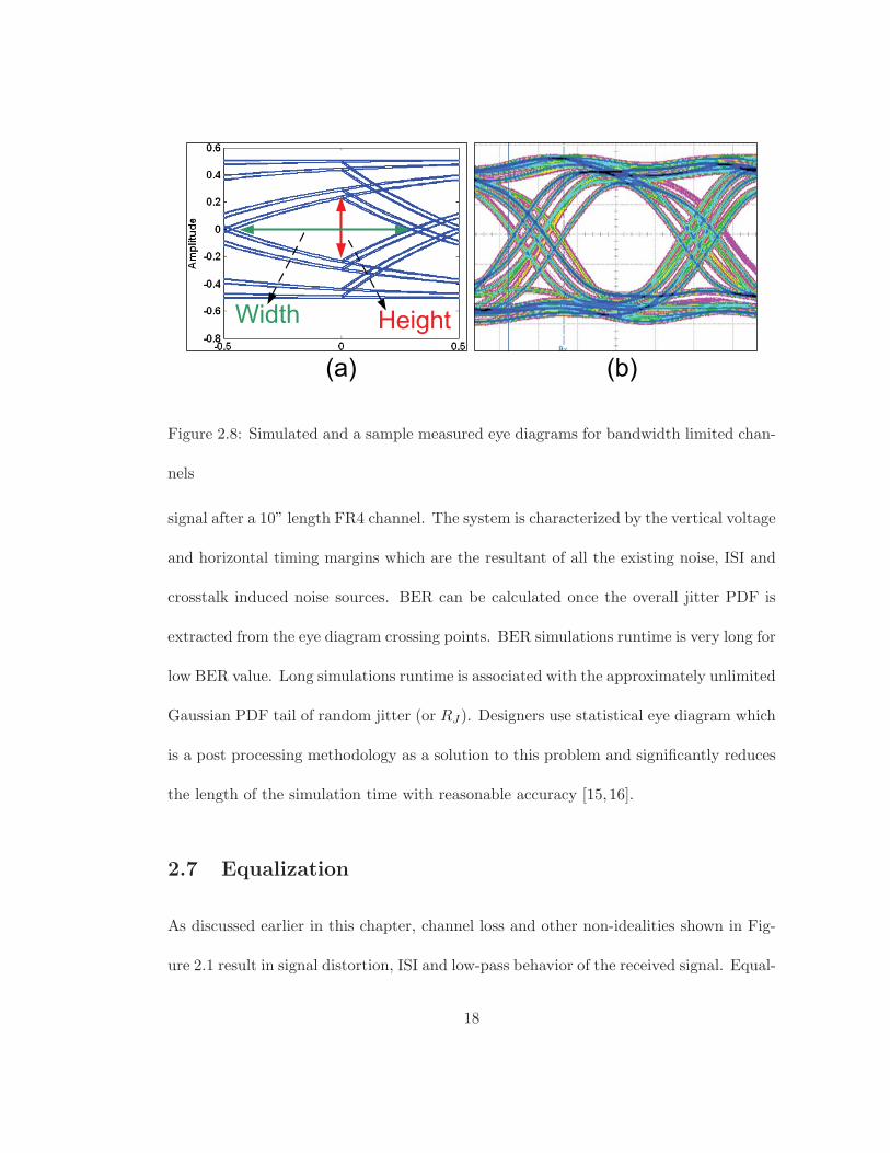
Figure 2.8: Simulated and a sample measured eye diagrams for bandwidth limited chan-
nels
signal after a 10” length FR4 channel. The system is characterized by the vertical voltage
and horizontal timing margins which are the resultant of all the existing noise, ISI and
crosstalk induced noise sources. BER can be calculated once the overall jitter PDF is
extracted from the eye diagram crossing points. BER simulations runtime is very long for
low BER value. Long simulations runtime is associated with the approximately unlimited
Gaussian PDF tail of random jitter (or RJ). Designers use statistical eye diagram which
is a post processing methodology as a solution to this problem and significantly reduces
the length of the simulation time with reasonable accuracy [15,16].
2.7 Equalization
As discussed earlier in this chapter, channel loss and other non-idealities shown in Fig-
ure 2.1 result in signal distortion, ISI and low-pass behavior of the received signal. Equal-
18

izers are compensation filters, normally with high-pass frequency response, which boost
high-frequency components of the channel and circuit blocks with limited bandwidth and
ideally result in an overall flat frequency response. In the time domain, equalizers tend to
suppress all ISI components of the overall system impulse and pulse response. Equaliza-
tion or bandwidth boosting can be performed either in the analog or the digital domain.
Analog equalizers are normally placed at an I/O receiver front-end combined with the
receiver amplifier. Capacitive degeneration or inductive peaking is used to implement
analog equalizers while incorporating zero-pole tuning capability. Although switching
speed, fT , of transistors in CMOS technologies is increasing but, parasitic capacitance
of metal interconnects becomes more pronounced and therefore the design of on-chip
inductor-less high-pass active filters becomes quite difficult at multi-GHz frequencies as
will be discussed in chapter 4. Analog equalizers can also be implemented using on-chip
high-pass passive filters but since filter characteristics are sensitive to mismatch and
quality factor, Q, of the passive elements, CMOS technology with low Q inductors can
not be a good candidate for these topologies implementation. In addition, tuning of high
frequency on-chip passive filters is not trivial. These facts along with major drive for in-
tegration of current systems makes the digital implementation of equalizers an attractive
alternative in CMOS technologies with programmable features. These high-pass filters
are normally implemented using finite impulse response (FIR) digital schemes with vari-
able number of taps. A combination of digital and analog equalization is used in current
practical solutions for high-speed links as will be discussed later in this section.
19

Figure 2.9: Equalizer techniques used in a today’s typical high-speed links
Figure 2.9 illustrates a typical high-speed I/O circuit while focusing on equalization
and signaling and Figure 2.10 shows the respective frequency and time domain responses
for each block. Transmit FIR equalizer, or pre-emphasis, is used to suppress some of
ISI components or mostly the precursors. Here, the cursor is defined to be the largest
tap in the impulse or pulse response. Since voltage headroom is limited by the power
supply at the output of I/O transmitters, FIR equalizer uses the energy in the main tap
to cancel out the ISI taps. Therefore, the pre-emphasis output is scaled based on power
supply value and the equalized signal has a lower amplitude than before equalization,
but with less or ideally no ISI components as shown in Figure 2.10. The amplitude
reduction or de-emphasis becomes more pronounced when more ISI taps are equalized
by using transmit equalization which puts an upper limit on the number of pre-emphasis
taps to be used at transmitter. FIR filters run on a sampling clock and their power
consumption is directly proportional to the number of taps which makes these filters
quite power hungry for high-speed applications. Hence there is a need to optimize the
number of taps depending on the application. This can encourage the placement of
FIR equalizers at the receiver instead of transmitter. But transmit FIR filters have an
20

Figure 2.10: Frequency and time domain responses of various equalizer techniques
advantage of running on a very low-jitter clock while the receiver digital equalizers use
a recovered clock for sampling which is subjected to various noise and jitter sources.
Therefore there is a tradeoff between the equalized signal amplitude and quality while
designing equalizers in the link.
Majority of precursor ISI components are suppressed by transmit or receive pre-
emphasis and also by analog equalizers. Non-linear equalizers such as DFE shown in
Figure 2.9 are commonly used in I/O applications to eliminate postcursor ISI components
without a penalty in the equalized signal amplitude. DFE uses previous decisions to
remove postcursor ISI components, and therefore is sensitive to error propagation which
theoretically can be eliminated by using pre-coding schemes at the transmitter. But
such schemes are rarely used in I/O applications due to the possible high implementation
costs [6].
Several well-known digital communication solutions can be used to optimize the FIR
filter tap values such as zero forcing equalization (ZFE), minimum-mean-square-error
21

(MMSE) and least mean square (LMS) algorithm for adaptation. Majority of current
high-speed links use ZFE which forces all precursor ISI components to zero and use
DFE to remove the postcursor ISI. This is suboptimal as any input noise source at the
equalizer input is boosted at the output. As will be discussed in chapter 3, MMSE solves
for a combined pre-emphasis and DFE tap values incorporating crosstalk noise into the
optimization problem and therefore does not blindly boost the noise. LMS algorithm
uses a metric such as eye-height, eye-width or the combination of both to constantly
update the equalizer’s tap values.
The current urge for higher speed I/Os, results in several system and circuit design
obstacles for a cost-effective solution. Some of these bottlenecks are summarized as fol-
lows. Increasing the I/O speed negatively impacts design of DFE circuits in terms of
power and also convergence to the first tap in the quantization loop. The first postcursor
tap needs to be ready at the DFE input for subtraction from the received signal in less
than a bit time Tbit which is constantly shrinking with increasing data rates. Loop un-
rolling relaxes this loop timing issue by using two parallel paths assuming two values of
“0” and “1” for slicing and a multiplexer which is driven once the decision is made [17].
Also as we explained in Section 2.4, crosstalk noise has a high-pass characteristic and
when applied to an equalizer response, a high-pass filter, its impact becomes more severe
and therefore reduces both voltage and timing margin of the signal at the receiver. In
chapter 3 we will present a more efficient equalization scheme, partial response equal-
ization, and tap optimization for channels with steep roll-offs with substantial far-end
22

crosstalk noise from neighboring channels, which improves eye openings at a given speed
and therefore the BER of the I/O systems.
2.8 Reference Clock Generation
I/O transmitters require a high-quality reference clock with minimal jitter as the clock
quality directly impacts the transmit signal at the driver output. Transmit clock is nor-
mally generated using either a ring or LC-tank based voltage controlled oscillator (VCO)
in a PLL circuit to generate the clock for I/O transmitter. Ring VCOs are attractive
as they potentially require a small area but exhibit higher power, phase-noise as well as
jitter values. LC-tank based VCOs can generate higher quality clock than ring based
VCOs for the same power and frequency because of inherent higher Q characteristics.
Reference side-band spurs in the generated clock spectrum, commonly existing in CP
PLLs due to mismatch in phase and frequency detector (PFD) and CP circuits, result
in deterministic timing jitter. The prior work in reducing the reference spur levels will
be explained in chapter 5 [18–20] and later a novel spur reduction technique will be
presented which shows significant improvement when compared to previously published
results.
2.9 Timing Recovery
Several timing recovery techniques such as CDR and DLL based circuits are normally
used to the received signal after partial equalization in current high-speed I/Os. Partial
23

Figure 2.11: Simplified closed-loop timing recovery circuit using an edge-based CDR
equalization is normally needed as the received signal may not have distinct data edges
and the eye may be closed in environments with severe ISI, and therefore edge-based
CDRs is not applicable. CDRs extract both frequency and phase from an incoming
stream of NRZ data. From a digital communications perspective, phase recovery of
incoming stream of symbols without the phase knowledge is a Maximum-Likelihood (ML)
optimization problem. In other words, a second order PLL is an ML phase estimator [6].
The power spectral density of incoming NRZ data stream at receivers in 2-PAM
signaling does not have any component at bit rate frequency; therefore, regular mixer-
based PLLs can not be used to recover the transmit clock. A bit rate tone is generated
in the power spectral density of the resultant signal after applying the NRZ data either
to a nonlinear or a differentiating device, where a PLL can now be used to lock onto this
produced tone. Simple signal differentiating and phase comparison can be performed by
using a flip-flop where the input is fed by the recovered clock and is sampled by NRZ
data [3]. NRZ data phase detection can also be done by delaying the incoming data and
24

applying an XOR function to NRZ data and its delayed version [3]. The first method
has a nonlinear and the latter one has a linear phase response. Almost all of today’s
commonly used phase detectors stem from these two basic techniques [3]. Figure 2.11
illustrates a basic edge-based CDR loop, similar to a PLL, where “PD” is the phase
detector, “CP” is the charge-pump, “LPF” is the low-pass filter. The loop recovers the
sampling clock from incoming NRZ data and uses this clock to re-sample the incoming
data through a D-flip flop (DFF) and generate the recovered data. Two commonly used
CDR phase detectors are Hogge (linear), and Alexander or bang-bang. Nonlinear, bang-
bang, phase detectors can be designed for higher speeds than linear phase detectors in a
certain technology because of the very limited bandwidth of XOR used in linear phase
detectors. But nonlinear phase detectors result in larger disturbances on VCO control
lines and therefore jitter as compared to linear phase detectors. CDR loops recover both
frequency and phase of incoming data stream in Plesiosynchronous systems. The loop
bandwidth needs to be at least equal to frequency difference of transmitter and receiver,
which is caused by crystal oscillator difference of about 300ppm. When incoming data
has a severe ISI, i.e. due to channel high-frequency loss, the recovered clock shows
considerable deterministic, data dependent, jitter. In order to suppress the deterministic
jitter components, the CDR bandwidth is usually reduced which inadvertently impacts
the CDR tracking capability. We will present a new CDR scheme and circuits in chapter 4
with a data independent jitter performance when the received signal is subjected to severe
ISI.
25

Figure 2.12: DLL based phase alignment circuit for per data channel timing recovery
Source-synchronous schemes use a forwarded clock signal for every bundle of data
where the number of data signals to be used with a forwarded clock signal is set by
the standard and system timing specifications. Frequency information is sent from the
transmitter to the receiver and the sampling clock phase is recovered by using a DLL
circuit in this scheme. Clock signal is usually sent at a fraction of data rate speed, and is
multiplied up to the bit rate frequency at the receiver using a multiplying PLL or DLL
which adds to the receiver power and area overhead. Figure 2.12 shows a DLL based
phase alignment circuit used in source-synchronous receivers, where the sampling clock
phase is recovered for each data line and the figure shows the closed loop timing recovery
for one data bit. Digital phase mixer or rotator blends multi-phase clock outputs and
feeds the interpolator inputs with two clock phases to produce the fine tune sampling
26

clock. The DLL circuit, phase aligner, has usually a very small bandwidth which al-
lows for tracking slow varying processes such as temperature. Our proposed CDR as
will be described in chapter 4 provides a novel low-power solution which is ISI indepen-
dent and obviates the existing clock channel overhead in source-synchronous systems by
transmitting both the data and clock over the same wire.
27
Chapter 3
Constrained Partial Response
Equalizers for High-Speed Links
The persistent demand for increasing data throughput in computer desktops and servers
has pushed high-speed serial links to the limits of their performance. Channel loss and
imperfections in the channel frequency response, due to impedance discontinuities, lead
to inter-symbol interference (ISI) and limit the overall link throughput. Additionally,
crosstalk from neighboring channels causes timing and amplitude errors at higher speeds.
All these non-idealities exacerbate the eye closure at the receiver and adversely affect the
BER of the overall link. Linear equalizers are often used in state-of-the-art high speed
links in order to ensure signal integrity [21]. As discussed in chapter 2, 2-PAM is the
most common modulation for interconnect communication with full channel equalization
where the combined response of the equalizers and the channel is forced to a single
28
impulse, i.e., zeroing out all ISI components [21–24]. More recently, duobinary and 4-
PAM equalization techniques have been applied in high-speed serial links [23, 24]. One
of the major goals of our research is to extend the use of the different equalization
techniques and demonstrate the potential benefits provided by PR channel equalization
for future high-speed links.
The successful use of PR equalization in disk drive channels is well reported [25,26].
Many of these techniques can also be applied to wireline communications when the link
performance is not limited by the used fabrication technology. For a fixed channel,
as the data rate increases, the number of post-cursor and precursor ISI components
increases. Partial response equalization allows some controlled amount of ISI, determined
by a known target PR, to remain in the equalized response. This is in contrary to
conventional full channel equalization, where all the ISI components are forced to be
zero [25,26]. When equalization is done in the transmitter side and in environment with
considerable crosstalk noise, this technique normally results in a larger eye opening at
the receiver. Power supply limitations in practical wireline systems place constraints
on the peak transmit power (peak transmit voltage) rather than the average power as
contrary to many digital communication theoretical analysis. Therefore, this constraint
should always be used when comparing wireline systems [7, 22].
In this chapter, a PR equalization and detection framework is presented that equalizes
channels to a near optimal target PR. In other words, the channel is shaped to be
close enough to the desired response, while limiting the architecture complexity for a
29

given channel. Practical non-idealities such as impedance discontinuities, crosstalk and
circuits noise are incorporated into the optimization problem. Based on our analysis, an
architecture suitable for a variety of channels is proposed which uses a linear equalizer at
the transmitter combined with a 1-tap DFE at the receiver. This architecture was applied
to a class of channels used in high-speed memory applications, and showed improved
performance when compared to full-channel equalization techniques. Additionally, the
new architecture mitigates the tight DFE loop timing issue and relaxes receiver circuit
design in terms of speed [27].
The constrained PR response equalization technique presented here improves eye
openings and reduces crosstalk impact for a large class of channels used, while main-
taining a simple implementation. Consequently the overall link bit error rate (BER)
reduces. The new proposed transceiver architecture is particularly well suited for high-
speed multi-channel applications due to the mitigated DFE loop timing constraint. In
comparison to duobinary equalization, the proposed PR architecture improves the eye
height and eye width of the receiver by 28% and 10% respectively at 10Gb/s and by
19% and 7% respectively at 15Gb/s. When compared to impulse equalization, the per-
formance improvements are even larger.
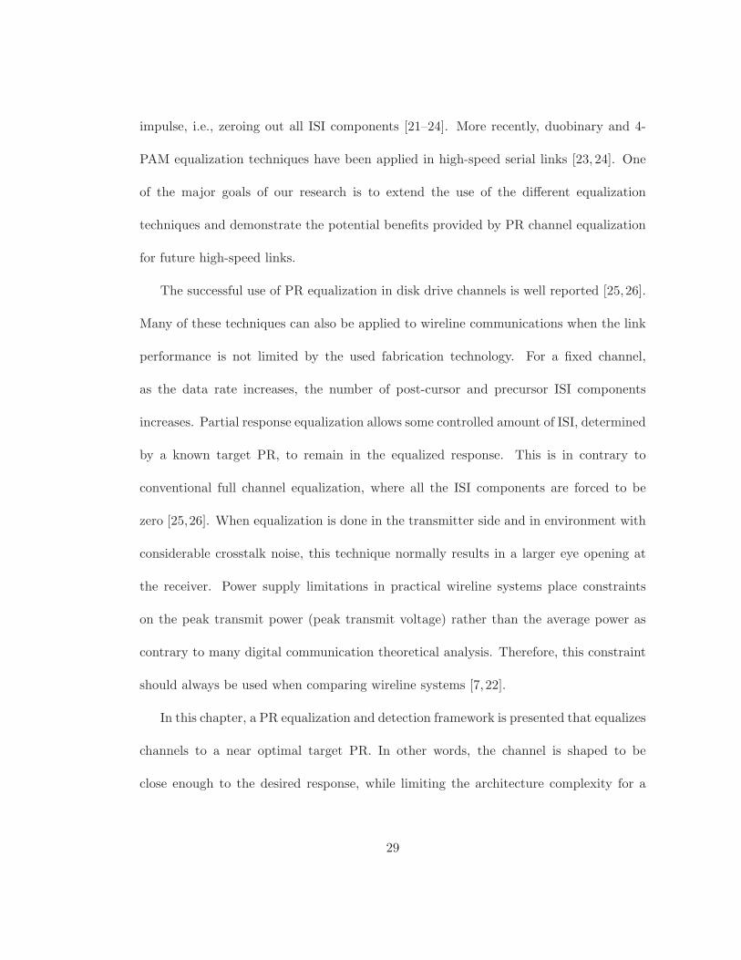
3.1 Generalized Partial Response Equalizers
In current day high-speed links, signal integrity issues are usually addressed by equalizing
the distorted signal as described in the previous chapter. The performance is improved
30
Figure 3.1: Generalized and constrained partial response equalization technique
31

20 30 40 50 60 70 80 900
0.2
0.4
0.6
0.8
1
Sample number
12" Microstripwith connectors20" Stripline 8" Stripline
Pulse amplitude (V)
Figure 3.2: Measured stripline and microstripline channel pulse responses
by increasing the number of taps in the transmit FIR equalizer or receiver DFE to
remove the majority of the ISI [21]. Full channel transmit equalization (PR1) to a
single impulse can result in a smaller eye opening in comparison to PR equalization
when the channel impulse/pulse response has strong ISI components. Figure 3.1 shows
a typical serial link channel pulse response which is equalized to a general target PR of
[b1.1.b2.b3.b4] (as the combined response of transmit equalizer and the channel), where
the bi’s are the tap values calculated by an optimization algorithm as will be explained
in section 3.3. As shown later in Figure 3.2, this response is fairly typical of measured
channels with risers and connectors. Forcing all the ISI taps to zero normally results
in a smaller eye opening when the channel pulse response is similar in shape to that
32

Figure 3.3: (a) General impulse response at T1−Symb and (b) at T2−Symb
shown in Figure 3.1. Not surprisingly, equalizing the pulse response to a target PR
closer to the channel pulse response, i.e. using a matched filter, results in a larger eye
opening at the receiver. Figure 3.1 also shows different PRs that can be used as the
target response during equalization. Here, PR1 is the full channel equalization, PR1.1 is
duobinary equalization [24], PR1.1.b2 is the proposed PR equalization and PRb1.1.b2.b3.b4
is the generalized target PR that can be used for higher speeds and certain channels.
In PR equalization, a predetermined amount of ISI is allowed to remain after equal-
ization which can be optimally detected by a maximum likelihood sequence detector
(MLSD). However, MLSD implementations are too complex and require extremely high
power for the speeds required in the state of the art serial links. We propose a novel link
architecture in section 3.3 for the PR1.1.b2 target, which can be used for a wide range
of channels. Figure 3.2 shows measured pulse responses for two stripline channels with
different lengths and a microstrip channel with connectors commonly used in high-speed
links. We noted that the measured pulse responses for the various channels look quite
similar to the model shown in Figure 3.1. Figure 3.3(a) and 3.3(b) illustrate typical
33

channel pulse responses at two different rates and their corresponding cursor (main tap),
precursor and postcursor ISI taps. The number of precursor and postcursor ISI compo-
nents are fewer at the lower symbol rate, 1T1−Symb
, therefore equalizing all the ISI taps to
zero results in little or no penalty in the eye opening at the receiver. At higher speeds,
1T2−Symb
, the number of ISI components increases as shown in the figure and equalizing
them to zero reduces the receiver eye opening. PR equalizers alleviate this issue, improve
eye opening, and limit noise boost. A new link architecture is required to address the
controlled ISI and perform detection. It is worthwhile noting that the implementation
complexity increases when dealing with a more general PR, hence there is a tradeoff in
determining the optimum PR to be used for a particular channel response. Additionally,
when the channel is equalized to a non impulse PR, both the overall occupied signaling
bandwidth and crosstalk are reduced. This is discussed in more detail in the next section.
3.2 Crosstalk in Partial Response Equalization
FEXT is one of the major high frequency noise sources which reduces the signal to
interference ratio in parallel high-speed links, [2]. Full channel transmit equalization
(PR1) is sub-optimal at higher speeds as it has a high-pass frequency response and
boosts the crosstalk noise which has high-pass response by nature as well. Figure 3.4
shows the frequency responses of the different PR equalizers when optimized for a given
channel with a fixed number of taps. As seen in the figure, PR1 equalizer boosts the
higher frequencies the most. The more generalized PR target equalizers suppress more
34

0 0.2 0.4 0.6 0.8 1-45
-40
-35
-30
-25
-20
-15
-10
-5
0
Normalized Frequency (××××ππππ rad/sample)
PR1PR1.1PR1.1.b1PRb1.1.b2PRb1.1.b2.b3.b4
PR EQ. frequencyresponse magnitude (dB)
Figure 3.4: Frequency response of different target PR equalizers
high frequency components. We define a figure of merit (FOM),yRx−rms
yXt−rms, which is the
ratio of RMS received signal to the RMS crosstalk noise from the adjacent lines (FEXT).
This FOM can be used to evaluate PR equalizer performance in high-speed links in the
presence of crosstalk. In fact, this FOM is the effective√SNR when crosstalk is the
dominant interference and noise component. Table 3.1 summarizes the FOMs for the
channel model discussed in [2] for different target PR equalizers. Due to the reduced
high frequency boost of the more generalized PR equalizer, they are particularly well
suited for link environments where crosstalk components dominate.
35

0 10 20 300
0.05
0.1
0.15
0.2
0.25
0.3
Sample number at 10Gb/s
Pulse amplitude (V)
Figure 3.5: Stripline and microstrip channel responses
Table 3.1: Crosstalk FOM for different PR equalization targets for the channel model
with 30” length and 20mil spacings [2]
PR 1 1.1 1.1.b2 b1.1.b2 b1.1.b2.b3.b4
yRx−rms
yXt−rms19 28 34 34 39
3.3 Novel Architecture for Memory Channels
For each of the measured responses shown in Figure 3.2, the number of ISI components
increase by increasing data rates and a target PR of [1 1 bopt] offers a reasonable match.
Here, bopt is the optimum b calculated using the minimum mean square error (MMSE)
optimization algorithm discussed in the next section. For the rest of this chapter we
36

0 5 10 15x 109
-90
-80
-70
-60
-50
-40
-30
-20
-10
0
Frequency (Hz)
8" Stripline20" Stripline12" Microstrip with Connectors
Channel frequencyresponse, S12 (dB)
Figure 3.6: Microstrip symbol rate pulse response at 10Gb/s
focus on the PR1.1.b target. This target is an extension to duobinary signaling (PR1.1)
and yet maintains reasonable implementation complexity. Figure 3.7 shows the proposed
architecture for the PR1.1.b target. Just as in duobinary, the precoder is a differential
precoder, which shapes the channel to 1/(1⊕
D) and results in the removal of the prior
bit history from the current symbol [28]. The precoder helps to reduce the receiver
overhead and makes it possible to decide the received data bit on a symbol by symbol
basis. Here, h is the victim channel impulse response and hXTl, ∀l 2 ≤ l ≤ m, are the
aggressor(s) (crosstalk) impulse responses. Pre-emphasis taps on the transmitter side
are optimized as explained in the next section. The detector at the receiver includes a
duobinary two-level slicer combined with some simple logic, which detects the transmit
37

data at each decision instant [24]. The impact of the known post-cursor tap, bopt, is
removed by using a 1-tap DFE and a post-coder which is identical to the pre-coder
shown in the Figure 3.7. The post-coder is needed in order to correctly cancel the
post-cursor ISI tap (bopt). The DFE post-cursor ISI tap (bopt) is delayed by two symbol
periods, i.e., the DFE loop timing constraint is relaxed by nearly 2X in comparison to
traditional DFE architectures. In traditional high-speed links, the DFE loop timing
is a critical implementation issue as the data rate increases. Loop unrolling which is
required to alleviate this timing problem results in increased power consumption due to
its parallel nature [17]. This proposed architecture is an alternative solution for high
speed operation in general and also to DFE loop unrolling due to the additional delay in
the feedback path which relaxes the loop timing problem normally associated with DFE
receivers.
Unfortunately, like other PR equalization schemes, timing recovery is not as straight
forward as full channel equalization since the incoming symbol is the weighted sum
of three consecutive bits and has multiple transitions and levels within each symbol
interval. An extended version of the timing recovery techniques developed for duobinary
and 4-PAM signaling may be required for improved performance [21, 23]. Pilot based
timing recovery [29] discussed in the next section can also be a suitable candidate for
PR signaling as it decouples the performance of timing recovery circuit from incoming
data edges. In this section we will primarily focus on channel equalization.
38
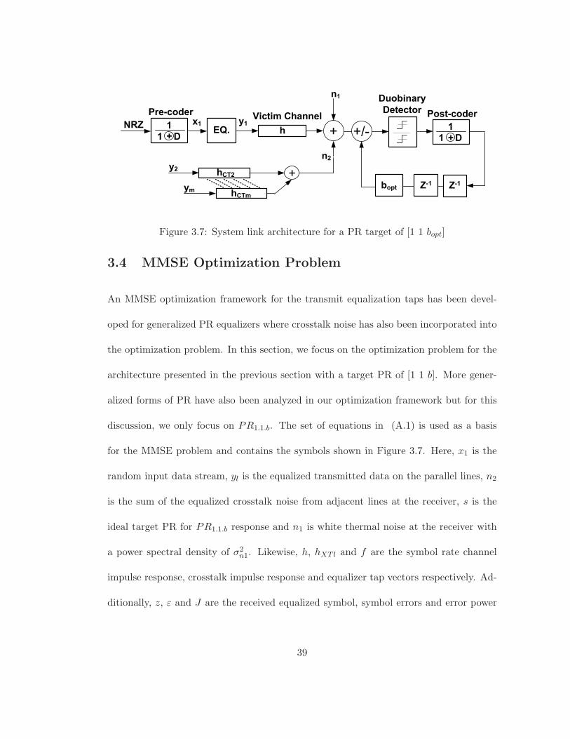
Figure 3.7: System link architecture for a PR target of [1 1 bopt]
3.4 MMSE Optimization Problem
An MMSE optimization framework for the transmit equalization taps has been devel-
oped for generalized PR equalizers where crosstalk noise has also been incorporated into
the optimization problem. In this section, we focus on the optimization problem for the
architecture presented in the previous section with a target PR of [1 1 b]. More gener-
alized forms of PR have also been analyzed in our optimization framework but for this
discussion, we only focus on PR1.1.b. The set of equations in (A.1) is used as a basis
for the MMSE problem and contains the symbols shown in Figure 3.7. Here, x1 is the
random input data stream, yl is the equalized transmitted data on the parallel lines, n2
is the sum of the equalized crosstalk noise from adjacent lines at the receiver, s is the
ideal target PR for PR1.1.b response and n1 is white thermal noise at the receiver with
a power spectral density of σ2n1. Likewise, h, hXTl and f are the symbol rate channel
impulse response, crosstalk impulse response and equalizer tap vectors respectively. Ad-
ditionally, z, ε and J are the received equalized symbol, symbol errors and error power
39

respectively.
yl(k) = (xl ∗ f)(k), ∀l 1 ≤ l ≤ m
n2(k) =
M∑l=2
(yl ∗ hXTl)(k)
s(k) = x1(k) + x1(k − 1) + bx1(k − 2)
z(k) = (x1 ∗ f ∗ h)(k) + n2(k) + n1(k)
ε(k) = s(k)− z(k) = x1(k) + x1(k − 1) + bx1(k − 2)−
(x1 ∗ f ∗ h)(k)− n2(k)− n1(k)
J = E[ε(k)ε(k)∗] (3.1)
The following criteria hold ∀i −L ≤ i ≤ L using the MMSE problem for symbol error
power, J , defined above.
∂J
∂f(i)= 0,
∂J
∂b= 0 (3.2)
E{[(h ∗ x1)(k − i) + n2(k − i)]ε(k)} = 0 (3.3)
Equation (3.3) follows the criteria in (3.2) with J as simplified in (A.1). Rearranging
the above equations leads to the following set of equations ∀i −L ≤ i ≤ L with bopt as
the optimum variable tap in the target PR1.1.b and fopt’s as the optimum pre-emphasis
tap values. Further details of these simplifications and relevant assumptions have been
40
explained in appendix A.
bopt =L∑
p=−Lfopt(p)h(2− p) (3.4)
h(−i) + h(1− i) =
L∑p=−L
fopt(p)
[∑m
h(m)h(m− p+ i)+
M∑l=2
∑v
hXTl(v)hXTl(v − p+ i)− h(2− p)h(2− i)
](3.5)
To provide a closed form expression for fopt, optimized taps vector, (3.4) can be written
in matrix form as shown in (3.6).
fopt = hv(H +HXT −H2)−1 (3.6)
The elements of hv and the square matrices H, HXT and H2 are defined for ∀i, p with
−L ≤ i, p ≤ L as follows.
hv(i) := h(−i) + h(1− i) (3.7)
H :=
[∑m
h(m)h(m− p+ i)
]pi
HXT :=
[M∑l=2
∑v
hXTl(v)hXTl(v − p+ i)
]pi
H2 := [h(2− p)h(2− i)]pi
Likewise, Jmin is obtained by replacing the equalizer tap vector (f) and the variable tap
value (b) with their optimum values for the J as shown in (A.1). Jmin is often used as
41
0 5 10 15 20 25
-20
-15
-10
-5
TX EQ. number of Taps
PR1
PR1.1
PR1.1.bopt
Figure 3.8: Jmin variation vs. number of TX equalization taps and different PRs
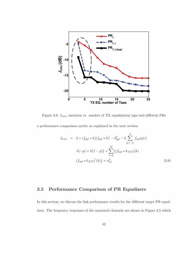
a performance comparison metric as explained in the next section.
Jmin = 2 + (fopt ∗ h)(fopt ∗ h)′ − b2opt − 2L∑
p=−Lfopt(p) {
h(−p) + h(1− p)}+M∑l=2
{(fopt ∗ hXTl)(k)
(fopt ∗ hXTl)′(k)}+ σ2
n1 (3.8)
3.5 Performance Comparison of PR Equalizers
In this section, we discuss the link performance results for the different target PR equal-
izers. The frequency responses of the measured channels are shown in Figure 3.5 which
42
-0.5 -0.4 -0.3 -0.2 -0.1 0 0.1 0.2-0.2
-0.1
0
0.1
0.2
UI
Slic
er in
put (
V)
-0.5 -0.4 -0.3 -0.2 -0.1 0 0.1 0.2.2
.1
0
.1
.2
UI-0.5 -0.4 -0.3 -0.2 -0.1 0 0.1 0.2.2
.1
0
.1
.2
UI
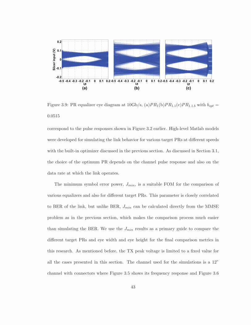
Figure 3.9: PR equalizer eye diagram at 10Gb/s, (a)PR1(b)PR1.1(c)PR1.1.b with bopt =
0.0515
correspond to the pulse responses shown in Figure 3.2 earlier. High-level Matlab models
were developed for simulating the link behavior for various target PRs at different speeds
with the built-in optimizer discussed in the previous section. As discussed in Section 3.1,
the choice of the optimum PR depends on the channel pulse response and also on the
data rate at which the link operates.
The minimum symbol error power, Jmin, is a suitable FOM for the comparison of
various equalizers and also for different target PRs. This parameter is closely correlated
to BER of the link, but unlike BER, Jmin can be calculated directly from the MMSE
problem as in the previous section, which makes the comparison process much easier
than simulating the BER. We use the Jmin results as a primary guide to compare the
different target PRs and eye width and eye height for the final comparison metrics in
this research. As mentioned before, the TX peak voltage is limited to a fixed value for
all the cases presented in this section. The channel used for the simulations is a 12”
channel with connectors where Figure 3.5 shows its frequency response and Figure 3.6
43

-0.5 -0.4 -0.3 -0.2 -0.1 0 0.1
-0.1
-0.05
0
0.05
0.1
0.15
UI
Slic
er in
put (
V)
0.5 -0.4 -0.3 -0.2 -0.1 0 0.1
1
5
0
5
1
5
UI-0.5 -0.4 -0.3 -0.2 -0.1 0 0.1
0.1
05
0
05
0.1
15
UI
Figure 3.10: PR equalizer eye diagram at 15Gb/s, (a)PR1(b)PR1.1(c)PR1.1.b with bopt
= 0.0613
shows its pulse response.
This channel is an example of commonly used channels in current high-speed links
and is used for the simulation results in the current section. In this example, there
is only small amount of crosstalk, intentionally by optimizing the interconnect design,
and therefore the residual ISI is the dominant factor in the eye closure at the receiver.
Figure 3.6 is the sampled pulse response of the discussed channel at 10Gb/s, which is
a close match for the target PR of [1 1 b]. For data rates above 10Gb/s and for the
current channel data, PR1.1.b performs better than both PR1 and PR1.1 equalizations.
The value of the optimized parameter, bopt, varies with the data rate. Figure 3.8 shows
Jmin values for the different target PRs for the given channel. For each simulation, Jmin
is illustrated while number of TX equalizer taps were changed.
As most of the recently published results on high-speed links use more than three pre-
emphasis taps, Figure 3.8 highlights the region for a practical number of pre-emphasis
taps. The figure shows a reduction in the minimum achievable symbol error power by
44

5 10 15 20 250
0.02
0.04
0.06
0.08
Data Rate (Gb/s)
Op
tim
ize
d V
ari
ab
le T
ap
(b
op
t)
Figure 3.11: Variation of optimized bopt versus data rate for the channel in Figure 3.4
using the more generalized PR equalizers. The best performance is provided by PR1.1.b
(lowest Jmin) when compared to PR1 and PR1.1 equalizations. PR equalizers with a
larger number of taps results in lower residual ISI and correspondingly lower Jmin. As
illustrated in the figure, Jmin does not improve for tap numbers greater than 15 due
to the complete cancelation of ISI. However, the difference in the performance floors
are due to the residual crosstalk, clearly illustrating the reduced noise boost caused by
PR1.1.b. Eye diagrams at the slicer input are a commonly used metric in high-speed
links for comparison purposes. As discussed in section 3.1 and illustrated in Figure 3.3,
increasing the speed changes the shape of pulse response and normally reduces the main
tap amplitude. Figure 3.11 depicts the variation of optimized feedback tap, bopt, for the
45

discussed channel versus data rate when it is been normalized with respect to the main
tap. The variation shape of bopt varies from one channel to another and a general trend
is not expected for all the channels.
Figure 3.9 shows the received slicer input eye diagrams at 10Gb/s using PR1, PR1.1
and PR1.1.b. The variable optimized tap, bopt, is canceled by a 1-tap DFE in PR1.1.b. As
seen in the figure, PR1.1.b has a larger eye opening when compared to PR1 and PR1.1
equalizations at 10Gb/s. Increasing the speed while keeping the number of TX PR equal-
izer taps unchanged leads to more residual ISI in PR1 equalization, which can further
reduce the RX eye opening as explained in section 3.1. Figure 3.10 shows the receiver
eye diagram for the PR1.1.b at 15Gb/s. As seen in the figure, while PR1 equalization
results in a completely closed eye at the receiver, PR1.1.b outperforms PR1.1 (duobinary)
equalization. The eye diagram results show the potential improvements offered by PR
equalization in current and future links at higher data rates. The improvements pro-
vided by PR equalizers are expected to be more pronounced at higher speeds and more
dense interconnects. A summary of the link simulations for the different equalization
strategies is shown in Table 3.2 for a typical 12” channel with connectors. At 10Gb/s,
PR1.1.b resulted in a 49% and 28% larger eye height and a 10% larger width when com-
pared to PR1 and PR1.1 equalizations, respectively. At 15Gb/s, PR1 equalization has
a completely closed eye. However, in comparison to PR1.1, PR1.1.b increases the eye
height by 19% and the eye width by 7%. These promising results combined with its
suitability for high speed and low complexity implementation shows that PR1.1.b is an
46

Table 3.2: Performance summary for 12” microstrip with connectors
PR Eye-H(mV) Eye-W(UI) Eye-H(mV) Eye-W(UI)
10Gb/s 10Gb/s 15Gb/s 15Gb/s
1 72.5 0.56 0 0
11 84.6 0.56 35.7 0.44
11b 108.2 0.62 42.7 0.47
excellent candidate for future high-speed multi-channel links.
3.6 Performance Comparison of PR Equalization with
Crosstalk Noise
In this section we focus on the performance evaluation of PR transmit equalization at
the presence of crosstalk noise. Unlike the previous section, the channel design was
not optimized for crosstalk effect and the spacing between the aggressor and the victim
channels were reduced to have an increased amount of crosstalk noises [27]. The first
experiment uses transmit PR1.1 equalization while crosstalk noises were not incorporated
in the MMSE optimization problem of section 3.4 although crosstalk noises were applied
to the victim channel.
The equalization taps have been calculated excluding the aggressors’ crosstalk noise
impact; therefore, we expect the result to be sub-optimal as discussed in section 3.2.
Figure 3.12(a) shows the result for this simulation setup. When incorporating the ag-
47

-0.5 0 0.5
-0.3
-0.1
0
0.1
0.3
UI
Sli
cers
in
pu
t
-0.5 0 0.5
-0.3
-0.1
0
0.1
0.3
UI
Figure 3.12: Impact of crosstalk noises on PR1.1 transmit equalization (a) Eliminating
crosstalk noises from MMSE problem (b) Including crosstalk noises in MMSE problem
gressors’ crosstalk noise in the MMSE optimization problem, calculated equalizers taps
are different from the previous case and eye height and eye width are improved by 38%
and 21.4% correspondingly as depicted in Figure 3.12(b). Figure 3.13(a) and 3.12(b)
show the result for the same simulation setup and when PR1.1.b was used for PR equal-
ization target. As shown in the figures, both eye height and eye width improved by
72.3% and 25% respectively. The improved eye opening for PR1.1.b versus PR1.1 is jus-
tified since 1.1.b is a better match for the used channel pulse response. Therefore the
ISI components are reduced and the impact of crosstalk noise sources are substantially
suppressed.
48

-0.5 0 0.5
-0.3
-0.1
0
0.1
0.3
UI
Sli
cer
Inp
ut
-0.5 0 0.5
-0.3
-0.1
0
0.1
0.3
UI
Figure 3.13: Impact of crosstalk noises on PR1.1.b transmit equalization (a) Eliminating
crosstalk noises from MMSE problem (b) Including crosstalk noises in MMSE problem
3.7 Summary
The benefits of PR equalization and the impact on crosstalk has been presented in this
chapter and a novel architecture for chip-to-chip I/O transceivers was proposed. The
receiver architecture for PR1.1.b relaxes the DFE loop timing issue, allowing for a speed
increase of nearly 2X compared to traditional DFE receiver implementations in the same
technology with little or no impact on the complexity. An MMSE optimization problem
was developed and PR equalizer performance was compared for some typical channel
cases. Our simulation results, based on measured channel responses, indicate that the
receiver architecture with a target PR of [1 1 b] outperforms both full channel (PR1) and
duobinary (PR1.1) transmit equalizations for a wide range of channels. Finally, using
PR1.1.b signaling suppresses crosstalk noise at the receiver due to inherent attenuation
characteristics of partial response equalizers as discussed in section 3.2 and illustrated
49

in section 3.6. PR equalization is a promising candidate for high-speed links which
can potentially reduce the crosstalk noise, by reducing the signaling bandwidth which
results in an increased receiver eye opening, and consequently lower BER. In addition, we
demonstrated that incorporating the crosstalk noise in the MMSE optimization problem
is critical and needs to be studied for individual channels. Incorporating crosstalk noises
when used with transmit PR equalization can enhance the eye opening at the receiver
and therefore improving the BER and the link performance.
50
Chapter 4
Pilot-Based CDR Scheme for
High-Speed Links
As discussed earlier in chapter 2, clock and data recovery techniques are used in Ple-
siosynchronous high-speed links where a frequency offset may exist between the trans-
mitter and the receiver [4]. Most high-speed serial links employ traditional edge-based
clock and data recovery techniques as discussed extensively in [3]. Clock frequency and
phase is extracted with the help of a PLL that detects and locks onto the transitions in
the received data pattern. The performance of such techniques, however, is dependent
on and limited by the quality of the data edges in the received signal. The transition
density of the received data is important to prevent the CDR from drifting. A common
technique to guarantee a minimum transition density is to utilize run length limited
(RLL) codes at the cost of reduced overall signal throughput [3].
51

CDR clock quality and power ultimately affects the timing margin, power efficiency
and performance of the high-speed link. In CDRs, the quality of the received data
transitions is important to reduce the deterministic jitter components in the recovered
clock. For example, residual ISI after equalization and crosstalk induced noise [12] at
the data transitions can negatively impact the quality of the recovered clock. A com-
mon approach to mitigate the effects of data dependent interference on the data edges
is to reduce the CDR bandwidth at the cost of reducing the CDR tracking bandwidth.
A second order CDR is normally used to track any frequency difference between the
transmitter and receiver in Plesiosynchronous systems. The CDR bandwidth is con-
strained to the frequency difference between the transmitter and receiver. Therefore,
data dependent jitter is not completely eliminated in the presence of large deterministic
interference. For example, large deterministic ISI in controlled-ISI signaling schemes
(duobinary [23, 24] and analog multi-tone [30, 31]), or in predictive DFE [32] can result
in bi-modal or multi-modal jitter distribution which further complicates the traditional
CDR hardware [32].
The clock can also be extracted from the data by passing the received NRZ data
through a nonlinear element to generate a tone at the bit rate frequency in spectral-line
clock recovery schemes [3]. A PLL is subsequently applied to lock onto the generated tone
using either linear or nonlinear phase detectors (e.g., mixers, D-flip-flops etc) [3, 33, 34].
Unfortunately, as discussed above, the tone generated from incoming data is disturbed
by both ISI induced noise and crosstalk from neighboring channels and requires a high
52

data transition density.
Source-synchronous, clock forwarding, is another technique which uses a dedicated
wire to carry the clock signal for a bundle of data wires as used in the HyperTransport
standard [10]. However, the overhead of the extra wire may be unacceptable in certain
standards. An alternative to source-synchronous techniques is embedded clock where
a clock tone is encoded in the transmit symbol and is extracted from the data stream
using a decoder at the receiver [35–37]. As a consequence, the design of high-speed low-
power CDRs that generate high-quality clocks continue to be a challenge in the design
of high-speed electrical links.
This chapter presents a novel pilot-based CDR scheme for high-speed chip to chip
communication, which alleviates the data and ISI dependencies of data-aided CDRs
without changing the data frequency spectrum and signaling levels. This technique
eliminates the overhead of an additional wire for the clock and does not require data
encoding and decoding while being compatible with most of available standards using
NRZ signaling [29,38]. A low-amplitude bit rate clock signal, i.e., a pilot, is added to the
transmit signal, placed at the notch of the NRZ data spectrum, and is sent over the same
channel as the transmit data. The synchronously transmitted clock tone is extracted at
the receiver using a novel low power circuit solution, which is used to drive the receiver
front-end samplers. The performance of the CDR technique is demonstrated using a
5Gbps differential receiver fabricated in a 0.13μm IBM CMOS technology. The technique
presented in this chapter decouples the clock recovery process from the equalization and
53

Figure 4.1: The proposed architecture using a pilot-based CDR with pilot frequency
equal to bitrate
data edge conditioning process at the cost of a small ≈5-10% pilot voltage overhead to
the transmitted data.
The rest of this chapter is organized as follows. The proposed architecture is described
in Section 4.1; while system-level design tradeoffs are presented in Section 4.2. A low
power circuit solution is described in Section 5.4 followed by the circuit design details for
the receiver blocks and the measurement results are presented in Section 5.5. Section 5.6
concludes the chapter and provides ideas for further development.
4.1 The Proposed Architecture
Figure 4.1 shows the block diagram of the proposed architecture. The transmitter sends
a low-amplitude narrow-band clock signal, the pilot, with the NRZ data over the same
channel [39]. The receiver front-end has two distinct parallel paths, one for clock recovery
and the other for data recovery. The clock recovery path includes a high-Q bandpass
filter at the pilot frequency which extracts the transmitted pilot signal and attenuates
54

the majority of the NRZ data energy and thermal noise away from the pilot. The
high-Q bandpass filter can be realized by using a PLL or an injection locked oscillator
(ILO), as will be discussed in the later sections, to lock on to the pilot signal. The
data recovery path uses conventional analog or digital equalization techniques, including
linear or nonlinear (DFE), to compensate for ISI. Since the pilot signal is periodic at the
bit rate, it appears as a DC component at the sampler within the receiver which can be
removed with DC offset cancelation techniques if needed. Although the pilot and data
are subjected to the same channel, they are not necessarily phase-aligned at the receiver
since the pilot is a narrow-band signal while the data is a wide-band signal. Therefore, a
phase-shifter (φ) needs to be placed either at the transmitter, delaying the pilot before
being added to data, or at the receiver, delaying the recovered clock, to adaptively adjust
the phase of the recovered clock as required.
The presented CDR architecture sends the frequency information to the receiver,
similar to source-synchronous technique; however, eliminating the need for an additional
wire carrying the clock signal. In addition, this proposed scheme, to first-order, decouples
the recovered clock performance from the data edges that are subjected to channel ISI
and other nonidealities at the cost of a voltage overhead at the transmitter. However,
as we will show later in Section 4.2, with the right choice of the pilot frequency, this
overhead could be minimal. In the following section we will discuss some of the design
tradeoffs for the proposed scheme.
55

4.2 System Level Analysis and Tradeoffs
The receiver for the proposed clock recovery path can be appropriately modeled as a
high-Q bandpass filter with a bandwidth of BWCDR. The input to the receiver is the
summation of the pilot, and the wideband NRZ data. From the clock recovery circuit’s
perspective, the pilot is the signal of interest and the wideband NRZ data along with
any electronic noise from the receiver front-end is the unwanted “noise”. The frequency
spectrum of the aggregated data and pilot for two different choices of the pilot frequency,
half bit rate and full bit rate pilot, are illustrated in Figure 4.2(a) and Figure 4.2(b)
respectively. The data induced disturbances are shown with dashed lines in Figure 4.2.
The data induced noise may be considerable when the pilot frequency is equal to half of
the bit rate as depicted in Figure 4.2(a). Ideally, the power spectral density of an NRZ
data stream at the output of the transmitter is a Sinc2(ω) function, which has zeros (or
notches) at the bit rate and integer multiples of the bit rate frequency. Therefore, the
choice of a pilot frequency that is placed at the NRZ data notch results in little or no
data induced energy within its vicinity as shown in Figure 4.2(b).
The high-Q bandpass filter can be realized using either a mixer-based PLL or an ILO
circuit. Section 5.4 describes in detail the ILO circuit implementation and its advantages
in comparison to the PLL. An accurate analytical noise model for an ILO circuit that
includes the detailed noise performance is not available. However, it is been shown that
the closed loop behavior of an ILO is similar to that of a first-order PLL [40], and for
this reason we shall use a PLL model for our system level analysis and design tradeoffs.
56

Figure 4.2: Frequency Spectrum of Aggregated NRZ data and pilot
The conclusions from this section can be applied to our circuit level implementation in
Section 5.4.
Figure 4.3(a) shows the mixer-based PLL and Figure 4.3(b) illustrates the respec-
tive mathematical model reported in [1] where the input is the summation of a narrow
band pilot signal with amplitude A and wideband noise with spectral density of N0.
In Figure 4.3(b), nD−BB(t) is the down-converted input noise, and Kd, Kv, F (s) are
phase detector (here mixer) gain, VCO gain and filter transfer function respectively. It
is worthwhile to note that the mixer gain impacts both the input signal and noise while
the input signal amplitude appears as a gain term only on the signal path.
For large SNR values at the input of the mixer-based PLL, the closed form variance of
the noise on the recovered phase is given by (4.1) [1]. As shown in (4.1), the loop gain has
a proportional term to the signal amplitude (A) which directly affects the feedback loop
57

Figure 4.3: Mixer base PLL receiver (a) Mathematical model presented by Viterbi (b) [1]
bandwidth. The impact of input signal amplitude on the bandwidth is determined by
the loop filter order. In a first-order system (F (jω)=1), for example, the loop bandwidth
is directly proportional to the signal amplitude (A).
σ2φ =
1
2π
∫ ∞
−∞N0
2| Kd.Kv.F (jω)/jω
1 +A.Kd.Kv.F (jω)/(jω)|2dω = N0BWCDR (4.1)
For the feedback loop of Figure 4.3(b), the recovered clock power is given by A2/2,
and it can be shown that the RMS jitter of the extracted clock (Jrms) is expressed
by (4.2) [1]. Here, BWData is the data bandwidth (which is proportional to the bit rate
and is assumed to be much larger than BWCDR), PnD is the received data power, A is the
received pilot signal amplitude, and β is a constant obtained from simulation. A is equal
to the transmit pilot amplitude times the channel attenuation at the pilot frequency. In a
first-order system, since BWCDR is linearly proportional to the received pilot amplitude,
58

the rms value of the jitter only improves with the square root of the pilot amplitude(√A). In higher order systems, the relationship would be slightly different, but is
always sub-linear. Equation (4.2) holds for an arbitrary choice of the pilot frequency
within the data bandwidth.
J2rms =
1
SNROut= β
2PnD
A2
BWCDR
BWData(4.2)
4.2.1 System Level Simulation
Several choices could exist for the pilot frequency. Equation (4.2) indicates that when the
data power within the CDR bandwidth is small, a smaller pilot amplitude is required
to achieve the same jitter performance. To investigate these choices the receiver was
modeled in Simulink/Matlab using a PLL. The data bandwidth was 5GHz and the PLL
used a second-order loop with a loop bandwidth of 40MHz. Additional PLL parameters
were selected to ensure a phase margin of 80◦ and appropriate stability. The ratio of the
pilot amplitude to the data amplitude was varied for two separate sets of simulations, for
a bit rate pilot and a half bit rate pilot as shown in Figure 4.2, while the data amplitude
was kept at a fixed value of “1V” peak. The recovered rms jitter was then measured for
each case as tabulated in Table 4.1. As shown in the table when the pilot is placed at
the bit rate frequency, data disturbance to the recovered pilot is minimal because of the
Sinc2(2πf) behavior of the data spectrum. For a pilot placed at the bit rate frequency,
a more accurate version of (4.2) can be derived as follows.
59
σ2Noise = N0BWCDR + α
∫ fBitrate+BWCDR
fBitrate−BWCDR
[Sin2(2π(f))
f2df ] (4.3)
The first term in (4.3) represents the thermal noise power within the CDR bandwidth
while the second term represents the integrated data induced noise within the CDR
bandwidth. Here α is a constant depending on the data peak to average ratio and
channel attenuation. This equation provides a good estimate of the thermal and data
induced noise around the recovered pilot at the receiver. The results of our system-
level simulations indicate that when the pilot frequency coincides with the signaling
bit-rate, between the two terms on the right hand side of (4.3), the first term is always
dominant. Therefore, in order to ensure a reasonable rms jitter power, the received pilot
power only needs to be sufficiently larger than the thermal noise that passes through
the high-Q bandpass filter. This lower limit is usually very small as compared to typical
signal levels used for transmission in high-speed links. Therefore, even for large values
of channel attenuation at the pilot frequency, a small pilot voltage overhead is imposed
on the transmitter to ensure that a good quality clock can be extracted at the receiver.
4.3 Prototype Circuit Design
In order to demonstrate the feasibility of the proposed clock recovery scheme, a fully
differential receiver was prototyped in a 0.13μm IBM CMOS process targeting data
rates of up to 5Gbps. Figure 4.4 shows the block diagram for the proposed receiver.
Tunable on-chip 50Ω resistors were used at the input to reduce matching reflections at
60

Table 4.1: System Level Simulation of Pilot Based CDR for the Cases Illustrated in
Figure 4.2
VPilotVData−pp
Jrms(%UI) Jrms(%UI)
fPilot = Rbit/2 fPilot = Rbit
25% 2.3 ∼ 0
20% 3.4 ∼ 0
10% Looses lock ∼ 0
1% Looses lock 0.18
the channel interface. The receiver has two separate parallel paths for clock extraction
and data recovery.
Our initial circuit-level analysis indicated a high area and power cost when the high-
Q bandpass filter was implemented using a PLL. An ILO, on the other hand, can achieve
the same bandwidth at substantially lower power [3, 41]. The core of an ILO is essen-
tially an oscillator, which consumes only a small fraction of the overall PLL power [41].
Additionally, ILOs can be designed to have extremely fast transient responses. As a
result, using an ILO in the receiver enables the system to quickly switch between sup-
ported data rates, and therefore, relaxes the tradeoff between the settling time and the
recovered clock jitter performance of the CDR [42]. Consequently, in this design we use
an ILO to implement the high-Q bandpass filter. ILOs can behave as extreme high-Q
filters; however, the output phase noise of an ILO is a strong function of the phase noise
of the injected signal. Although there is a null in the NRZ data at the bit rate frequency,
61

some phase disturbance is possible due to the Sinc2(2πf) behavior of the NRZ data
spectrum. Therefore, to further reduce the impact of the NRZ data on the recovered
clock, the ILO is driven by a pre-filtered version of the received pilot and data signal.
We take this approach to both clean up the injected signal and amplify its amplitude.
Since the locking range of ILO circuits depend on the noise level of the injection
signal [41,42], the received signal, disturbed by the noise from NRZ data in our architec-
ture, needs to be filtered. Also cascaded ILO circuits can not be used in this architecture
due to their very narrow overall locking range behavior, and therefore, there is a need
for a tuned filter to remove the NRZ data disturbance from the received signal. The
output of this filter is then used to injection lock the VCO.
The clock extraction path is preceded by a low-Q passive parallel bandpass LC filter,
for power matching and to suppress some of the data energy around the pilot signal and
is similar to many narrow-band RF LNA designs [43]. The matching circuit is followed
by an LC-tuned amplifier shown in Figure 4.5 to further suppress the noise from the
NRZ data. Current mode logic (CML) buffers at the output of the tuned amplifier in
Figure 4.4 are used to decouple the oscillator from the previous stages and extends the
achievable ILO bandwidth. The buffered output is then used as an injection signal for
the injection-locked oscillator. As will be discussed in the next sub-sections, both the
LC-tuned amplifier and the VCO use the same inductor that has been optimized for
the designed data rate. MOS varactor values and areas were chosen to be optimum for
the tuning range and link performance. The subsequent sub-sections discuss the circuit
62

Figure 4.4: The proposed 5Gb/s prototype receiver using an injection locked oscillator
details for the various receiver blocks.
4.3.1 LC-Tuned Amplifier
Figure 4.5 shows the LC-parallel matching at the buffer output and the input of the
shown LC-tuned amplifier as depicted in Figure 4.4. Partial positive feedback [44] was
used to enhance the amplifier gain because of the finite quality factor (Q) of the on-chip
inductors in the design kit. The cross-coupled PMOS transistors M1 and M2 introduces
a negative resistance which cancels part of the loss of the LC tank and increases the
output amplitude.
The cross-coupled negative resistance is inversely proportional to its small signal
transcondctance gm1,2, which increases by reducing the current passing through the cross-
coupled pair. Reducing the tail current reduces the LC-tuned amplifier gain; therefore,
M3 and M4 shown in Figure 4.5 are used to carry some of the tail current and increase
the cross-coupled PMOS load negative resistance. This enhances the Q of the overall
63

Figure 4.5: Differential LC-tuned amplifier
LC-tuned amplifier for a fixed amount of power consumption. Oscillation was avoided by
ensuring that the cross-coupled pair canceled only part of the overall loss in the LC-tank.
4.3.2 Injection Locked Oscillator
Figure 4.6 shows the ILO design, which comprises of a core LC tank based VCO with
N-MOS and P-MOS cross-coupled transistors. M1 and M2 are the signal injection tran-
sistors which were sized to ensure low injection operation for the ILO [42]. Using both
N-MOS and P-MOS cross-coupled devices in the VCO improves the flicker noise related
phase noise component of the designed VCO [43].
64

Figure 4.6: Injection locked based oscillator
Equation (4.4) shows the closed form equation for the ILO locking range, fLock (here
BWCDR or the receiver bandwidth), where Q is the loaded oscillator tank Q, IInj is the
signal injected into the ILO and IOsc is the oscillator signal current [41].
ωLock = BWCDR =ω0
2Q
IInjIOsc
(4.4)
Oscillator current, IOsc was initially chosen to sustain the oscillation at nominal clock
frequency of the link at 5GHz. A ratio of 1/5 was chosen forIInj
IOscand the ratio of M1/M2
was chosen to ensure injection locked oscillation for the minimum received pilot signal
to data ratio which is 5% for this design.
ILO locking range was enhanced substantially by removing the VCO cell tail current
due to an increased overdrive voltage of M1 and M2 and therefore largerIInj
IOscfor a fixed
65

IOsc. This was verified through Spectre simulation and by subjecting the clock extraction
circuit including the ILO to the combined data and pilot signals.
Identical inductors were used in the VCO and the LC-tuned amplifier. The Q of the
inductors were optimized to operate at 5GHz. As shown in the Figure 4.6, varactors
were used for the fine tuning of both the LC-tuned amplifier and the VCO free-running
frequencies. A coarse tuning loop can be used at the system startup to bring the VCO
free-running frequency within the designed locking range of the receiver (BWCDR). In
our experimental system we used an off-chip analog tuning circuit to bring the initial
VCO free-running frequency within the desired receiver locking bandwidth at startup.
4.3.3 Source Degeneration Amplifier and Analog Equalizer
The data recovery path incorporates a capacitive source degeneration amplifier shown in
Figure 4.7, which boosts high frequencies and serves as an analog equalizer. Post-cursor
ISI components are reduced as a result of using this analog equalization. Equation (4.5)
shows the closed form frequency dependent gain of the source degeneration amplifier
with the load impedance of RL and CL and source degeneration impedances of Rs and
Cs.
Av(s) =gmRL
1 + gmRs/2
1 + sRsCs
1 + sRs(Cs+Cgs)1+gmRs/2
1
1 + sRLCL(4.5)
The ratio of the pole to zero is given by Equation (4.6), which is directly related
66

Figure 4.7: Source degeneration and analog equalizer
to the transconductance of the stage for gmRs 1 and inversely related to the ratio of
the input capacitance to the source degeneration capacitance. Increasing the amplifier
gain also increases the input capacitance of the differential stage and therefore limits
the maximum achievable separation of the pole and zero. The analog equalizer zero
placement was optimized for the bandwidth extension at the desired data rate.
Ps
Zs=
1 + gmRs/2
1 + Cgs/Cs(4.6)
4.3.4 CML D-Flip-Flop
The output of the equalizer is sampled using a CML D-flip-flop, which consists of master
and slave latches. The CML latch stage has been shown in Figure 4.8, which is clocked
by the recovered clock from the transmitted combined data and pilot. CML latches can
67

Figure 4.8: CML latch used in a master-slave D-flip-flop
be designed to operate close to 1/5th of the fT of the used process techonlogy. This
fast operating frequency is possible since the output swing value is only a fraction of the
supply voltage in CML logics. In addition, this logic family is known to be insensitive to
power supply noises as the current drawn from the power supply is the same regardless
of the output logic level [3]. The CML latch shown in Figure 4.8 comprises of two stages
of sample; differential transistors M1 and M2 form a sampler and cross-coupled pair
transistors M3 and M4 function as a hold stage. It is northworthy that CML latches
have two different time constants. When the CML latch is in the sampling phase, the
output time constant is determined by the load resistance and capacitance of RL and
CL. The load capacitance comprises the CML latch output intrinsic capacitance which is
68
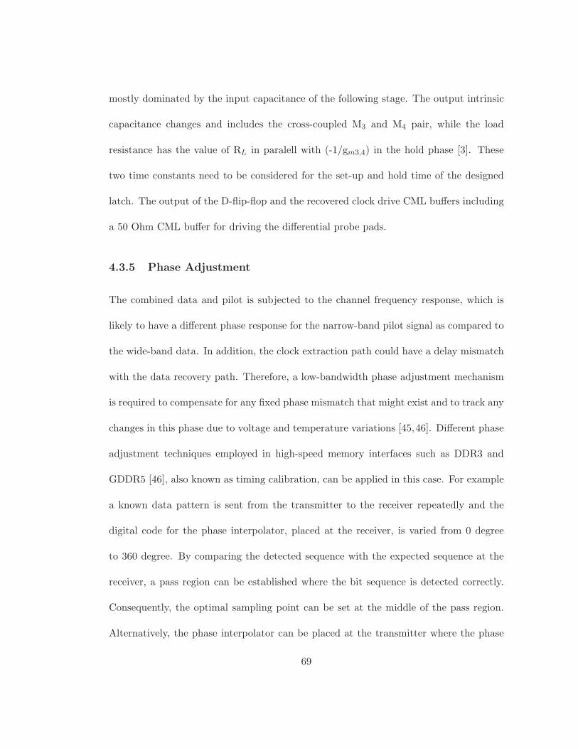
mostly dominated by the input capacitance of the following stage. The output intrinsic
capacitance changes and includes the cross-coupled M3 and M4 pair, while the load
resistance has the value of RL in paralell with (-1/gm3,4) in the hold phase [3]. These
two time constants need to be considered for the set-up and hold time of the designed
latch. The output of the D-flip-flop and the recovered clock drive CML buffers including
a 50 Ohm CML buffer for driving the differential probe pads.
4.3.5 Phase Adjustment
The combined data and pilot is subjected to the channel frequency response, which is
likely to have a different phase response for the narrow-band pilot signal as compared to
the wide-band data. In addition, the clock extraction path could have a delay mismatch
with the data recovery path. Therefore, a low-bandwidth phase adjustment mechanism
is required to compensate for any fixed phase mismatch that might exist and to track any
changes in this phase due to voltage and temperature variations [45,46]. Different phase
adjustment techniques employed in high-speed memory interfaces such as DDR3 and
GDDR5 [46], also known as timing calibration, can be applied in this case. For example
a known data pattern is sent from the transmitter to the receiver repeatedly and the
digital code for the phase interpolator, placed at the receiver, is varied from 0 degree
to 360 degree. By comparing the detected sequence with the expected sequence at the
receiver, a pass region can be established where the bit sequence is detected correctly.
Consequently, the optimal sampling point can be set at the middle of the pass region.
Alternatively, the phase interpolator can be placed at the transmitter where the phase
69

Figure 4.9: On-chip combination of data and pilot at the transmitter
of the data and pilot can be adjusted to achieve phase alignment at the receiver. For
the prototype system described in this chapter, we adopted the latter approach using
an off-chip phase trimmer at the transmitter as will be shown in the next subsection.
Since the required bandwidth for the phase adjustment circuit is relatively low, all of
our claims for the performance of the pilot based CDR scheme remains valid. Another
proposed solution for the low speed phase adaptation circuit used at the receiver will be
discussed in chapter 6.
4.3.6 Transmitter with Power Combined Pilot and NRZ Data
Before we present the experimental results for the designed chip in the next section,
we discuss the generation of the power combined pilot and data at the transmitter. As
shown in section 4.1, the pilot and data can be simply combined at the transmitter and at
the output of the final buffer stage. This summation can be done in the current domain
70

Figure 4.10: Off-chip combination of data and pilot at the transmitter with phase ad-
justment
using two CML buffers in parallel as depicted in Figure 4.9 along with the simulated
output waveform. As seen here, the pilot appears as a small sinusoidal waveform on top
of NRZ data at the output of the transmitter.
The combined data and pilot can also be generated off-chip which was used for
testing the current designed chip as illustrated in Figure 4.10. Off-chip phase trimmers,
adjusters, were used at the transmitter and before power combination. As shown in the
figure, the differential output data from PRBS was power combined with the generated
differential clock. The resulting power combined data and pilot was applied to the used
channel followed by the designed receiver chip.
4.4 Experimental Results
Figure 4.11 shows the chip micrograph with the receiver circuits highlighted. The overall
receiver area is 0.2914mm2, and consumes 25.75mA from a 1.5V supply while operating
at 5Gbps. The pilot-based CDR alone occupies 0.171mm2 and consumes 11.75mA from
71

the 1.5V supply. In order to test the prototype receiver, the data generated from a
CENTELLAX PRBS generator was differentially power combined with an attenuated
input clock signal, i.e., the pilot, to the PRBS as illustrated in Figure 4.10. We used
off-chip phase trimmers and attenuators at the transmitter and before power combining
to ensure the synchronization of transmit data and pilot. The resulting power combined
data and pilot signal was applied to the channel and received by the prototype chip. The
prototype chip was placed in an QFN5x5 32A open cavity package, and then the power
combined PRBS data and pilot signal after passing through the appropriate channel was
applied to the receiver using GSSG probes.
During initial setup, the PRBS was turned off and the receiver was tuned to have a
high-Q and low bandwidth, to focus on the transmitted pilot frequency operated at the
data rate. The power combiners and splitters before the channel contribute 11dB of loss
at 5GHz.
In order to measure the performance of the architecture presented in this chapter in
the face of variable ISI levels, we measured the recovered clock performance for different
lengths of FR4 lines. We ensured a constant pilot to data ratio for all cases. The three
measurements of rms jitter were 1.3ps, 1.5ps and 1.6ps for FR4 channel lengths of 0”,
5” and 10” respectively, while the deterministic jitter component of the recovered clock
remained virtually unchanged at 0.1ps for all cases. The oscilloscope was triggered with
a clean clock for these tests. These measurements confirm our claims in Section 4.1
that the proposed technique is relatively insensitive to ISI levels in the incoming data.
72
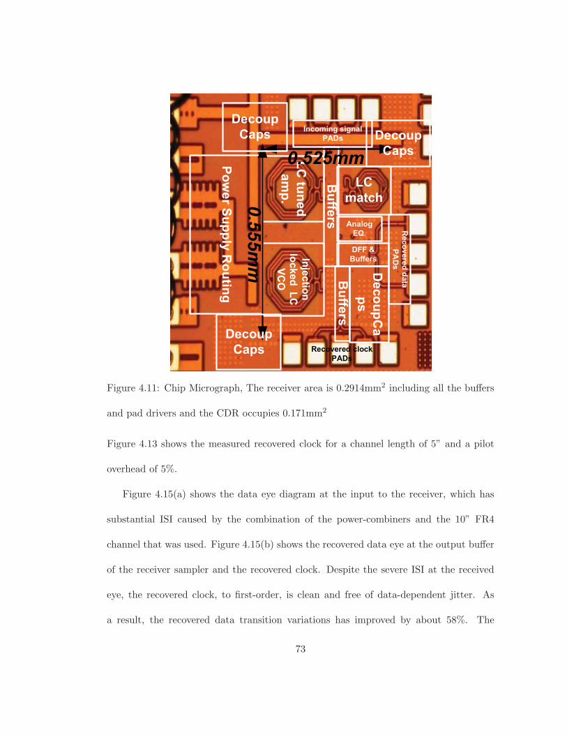
Figure 4.11: Chip Micrograph, The receiver area is 0.2914mm2 including all the buffers
and pad drivers and the CDR occupies 0.171mm2
Figure 4.13 shows the measured recovered clock for a channel length of 5” and a pilot
overhead of 5%.
Figure 4.15(a) shows the data eye diagram at the input to the receiver, which has
substantial ISI caused by the combination of the power-combiners and the 10” FR4
channel that was used. Figure 4.15(b) shows the recovered data eye at the output buffer
of the receiver sampler and the recovered clock. Despite the severe ISI at the received
eye, the recovered clock, to first-order, is clean and free of data-dependent jitter. As
a result, the recovered data transition variations has improved by about 58%. The
73

Figure 4.12: Designed test board using open cavity QFN5x5 32A and probing the input
combined data and pilot and recovered clock and data
same experiment was repeated for a differential 5” FR4 line, (i.e., much lower ISI) while
keeping the transmit pilot at the same level. The recovered data ISI was improved by
about 45% while maintaining the BER of 10−12.
The CDR bandwidth was measured by changing the transmit clock frequency (chang-
ing both the bit rate and pilot frequency), and the effect of pilot amplitude and loop
bandwidth was verified by changing the transmit pilot amplitude as shown in Figure 4.16.
The bandwidth varies linearly as predicted by injection-locking theory discussed earlier
in Section 4.2. The CDR bandwidth can also be changed by altering the tuning for
the amplifier and/or VCO to accommodate the various desired values. The recovered
clock rms jitter of the pilot-based CDR was measured while varying the pilot ampli-
74

Figure 4.13: Recovered clock for pilot to data overhead of 5% and FR4 length of 5”
tude at the transmitter side and keeping the data amplitude fixed at 1Vpp as shown in
Figure 4.17. The figure also shows the transmitted pilot rms jitter of our signal source
generator, which places a lower bound on the recovered rms jitter at the receiver. The
oscilloscope was triggered by an ideal clock for this measurement. To achieve a 1.6ps and
1.2ps (0.8%UI and 0.6%UI) jitter at the receiver, a 5% and 11.7% voltage overhead is
required respectively at the transmitter when the overall channel loss is 10dB at 5GHz.
Any residual ISI components in the recovered data not equalized by the analog equalizer
can be further suppressed by using an additional decision feedback equalizer if needed.
Because of the large jitter of our source, we suspect that the absolute measured rms jitter
value for our prototype is likely to improve by using a better quality signal generator.
75
Figure 4.14: Eye diagram after power splitters and without FR4 channel (a) recovered
clock and data, data transition uncertainties improvement of about 50%(b)
In another experiment, a set of measurements was performed for a FR4 channel
length of 10” while PRBS lengths were changed (causing different ISI levels) i.e. 27 − 1,
215 − 1, 223 − 1 and 231 − 1. The measured deterministic jitter components remained
the same for all the measured cases. The PRBS pattern was also turned off and the
deterministic jitter on the recovered clock was compared with the case when PRBS was
76

Figure 4.15: Received eye diagram after power splitters and a 10” FR4 channel (a)
recovered clock and data, data transition uncertainties improvement of 58%(b)
77

20 40 60 8010
15
20
25
30
35
40
45
50
55
Received Pilot (mVpp)
Lo
ck
ing
Ra
ng
e (
MH
Z)
Figure 4.16: Pilot-based CDR bandwidth variation versus received pilot amplitude for a
fixed transmitted data amplitude
on and no significant change was observed. These measurements further justify our
claim in Section 4.1 that pilot-based CDR architectures are insensitive to deterministic
patterns and ISI components.
4.5 Summary
A novel pilot-based CDR scheme for high-speed electrical links is proposed in this chap-
ter, which alleviates the dependency of traditional edge-based CDRs on the quality of
78
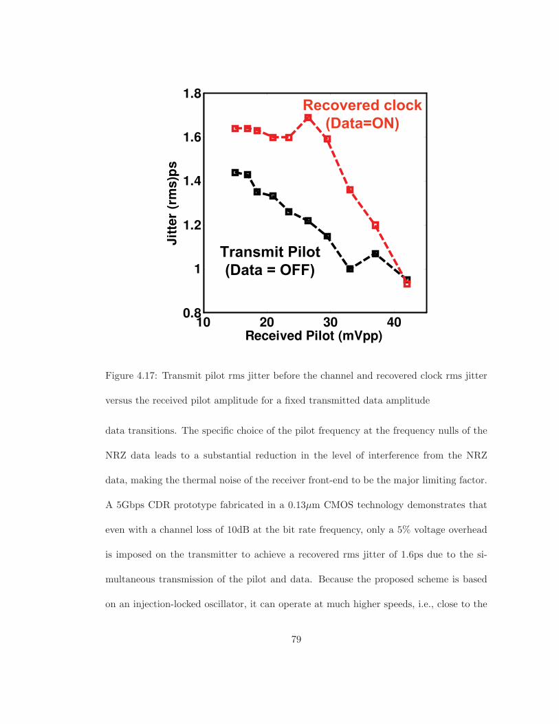
10 20 30 400.8
1
1.2
1.4
1.6
1.8
Received Pilot (mVpp)
Jit
ter
(rm
s)p
s
Figure 4.17: Transmit pilot rms jitter before the channel and recovered clock rms jitter
versus the received pilot amplitude for a fixed transmitted data amplitude
data transitions. The specific choice of the pilot frequency at the frequency nulls of the
NRZ data leads to a substantial reduction in the level of interference from the NRZ
data, making the thermal noise of the receiver front-end to be the major limiting factor.
A 5Gbps CDR prototype fabricated in a 0.13μm CMOS technology demonstrates that
even with a channel loss of 10dB at the bit rate frequency, only a 5% voltage overhead
is imposed on the transmitter to achieve a recovered rms jitter of 1.6ps due to the si-
multaneous transmission of the pilot and data. Because the proposed scheme is based
on an injection-locked oscillator, it can operate at much higher speeds, i.e., close to the
79
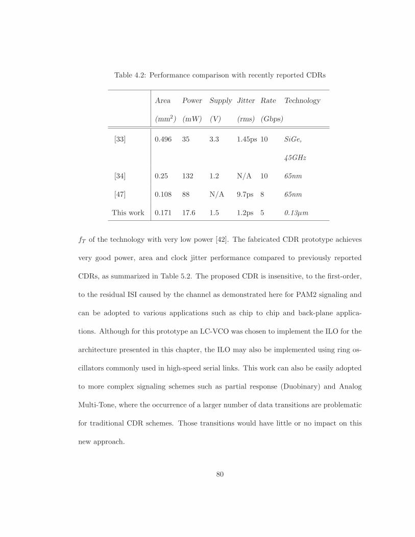
Table 4.2: Performance comparison with recently reported CDRs
Area
(mm2)
Power
(mW)
Supply
(V)
Jitter
(rms)
Rate
(Gbps)
Technology
[33] 0.496 35 3.3 1.45ps 10 SiGe,
45GHz
[34] 0.25 132 1.2 N/A 10 65nm
[47] 0.108 88 N/A 9.7ps 8 65nm
This work 0.171 17.6 1.5 1.2ps 5 0.13μm
fT of the technology with very low power [42]. The fabricated CDR prototype achieves
very good power, area and clock jitter performance compared to previously reported
CDRs, as summarized in Table 5.2. The proposed CDR is insensitive, to the first-order,
to the residual ISI caused by the channel as demonstrated here for PAM2 signaling and
can be adopted to various applications such as chip to chip and back-plane applica-
tions. Although for this prototype an LC-VCO was chosen to implement the ILO for the
architecture presented in this chapter, the ILO may also be implemented using ring os-
cillators commonly used in high-speed serial links. This work can also be easily adopted
to more complex signaling schemes such as partial response (Duobinary) and Analog
Multi-Tone, where the occurrence of a larger number of data transitions are problematic
for traditional CDR schemes. Those transitions would have little or no impact on this
new approach.
80

Chapter 5
Low Spur Single-Ended
Charge-Pump PLL
Increasing demand for competitively cheap and highly integrated solutions for wired
and wireless applications drives communication ICs in industry for various applications.
CMOS technology is the optimum choice for mass production because of its relative
low fabrication cost and high integration capacity; therefore, normally CMOS is used
in systems on a chip, SOCs, which are designed to meet a certain standard application.
The overall performance of SOCs poses a range of constraints on their composed sub-
system circuits design. PLLs are commonly used to generate a clean reference signal in
majority of today’s SOCs. The spectral purity of PLLs is critical in determining the jitter
quality of wired communication systems as well as the level of inter-channel interference
and blocking characteristics in wireless systems. In traditional integer-N charge-pump
81

PLLs, the degradation of spectral purity is primarily due to reference spurs, which are
caused by the inherent mismatch between “Up” and “Down” currents. current. This
mismatch results in unequal duration of current correction pulses in the loop since the
net positive charge deposited onto the loop filter is bound to be equal to the net negative
charge in locked condition. To lower the spur level, sample-reset loop filters with two
separate charge-pump paths have been implemented to decouple the charge-pump from
the VCO control line [19]. Another technique has also been proposed in [20], which
uses two feedback loops and two op-amps in the charge-pump to lessen the impact
of the current mismatch, thereby suppressing the reference spurs. However, both spur
reduction techniques increase circuit complexity, decrease voltage headroom, and require
additional area overhead. The charge-pump in [20] uses two feedback loops and two op-
amps to suppress the reference spurs. The combination of a unity gain voltage follower
and a replica bias circuit with current feedback is used to reduce the impact of current
mismatches. Additionally, the circuit has limited voltage headroom due to the stacking
of six transistors. According to the ITRS, future technologies will use supply voltages of
less than 1V [5]. Clearly, voltage headroom is going to be a major problem as we move
to lower supply voltages.
In this chapter, we propose a novel spur reduction technique that results in significant
reduction of side-band spurs, with minimal overhead to traditional single-ended charge-
pump PLLs. A feedback correction circuit has been incorporated into the charge-pump
to alleviate the mismatch in the “Up” and “Down” currents, thereby significantly at-
82

tenuating the reference spurs. Prototype PLLs operating at 5.6 GHz with and without
this technique have been designed and fabricated in a 0.18μm CMOS process technology.
The proposed technique is shown to reduce reference spurs by 22 dB with a measured
spur level of -66 dBc/Hz. Our proposed technique uses two transistors less in stack al-
lowing for a supply voltage that is roughly 0.4V lower than the design reported in [20].
Additionally, this technique uses only one negative feedback loop (i.e., one amplifier)
to dynamically suppress the disturbance on the VCO control line, thereby limiting the
power and area overhead.
5.1 Spur Generation in Single-Ended PLLs
Reference spurs is one of the main factors that degrades the spectral purity of PLLs.
Reference spurs are normally generated by a mismatch in phase and frequency detector
(PFD)/charge-pump circuit paths, which leads to a periodic disturbance, with the update
frequency equal to the reference input, on the VCO control line. The periodic disturbance
is most accurately modeled by an impulse train with the reference input frequency as
illustrated in (5.1). Here ω0 is the locked carrier frequency, ωRef is the frequency of
reference signal with the reciprocal period of TRef , KV CO is the VCO gain and Im is
the magnitude of periodic disturbances on the VCO control line. The magnitude of the
reference spurs, Vm, at (ω0 ± ωRef ) can be simplified by approximating the first harmonic
in Fourier series expansion of the impulse train (narrow-band FM), as shown in (5.2).
Vm ideally can be zero when there is no mismatch in the PFD/charge-pump paths.
83

Figure 5.1: Traditional PFD used in charge-pump PLL. Td or duration of correction
pulses generated in traditional PFD
VOut(t) = A0 cos(ω0t+ ImKV CO
∫ t
−∞
∞∑k=1
δ(t− kTRef )dt) (5.1)
Vm(t) ≈ A0ImKV CO
2ωRef[cos(ω0 + ωRef )t− cos(ω0 − ωRef )t] (5.2)
The PLL loop parameters such as VCO gain and charge-pump current define the
overall loop bandwidth. Quite clearly, there is a tradeoff between VCO gain, loop settling
time, VCO tuning range and the minimum achievable spur level as shown in (5.2).
Switched-capacitor based stabilization zeros are a potential technique that can be used
with charge-pump PLLs to relax the tradeoff between settling time and spur levels [19].
84

The direct coupling of the charge-pump circuit to the VCO control line, reflected
in the Im term in the above equations limits the achievable spur level in traditional
PLL designs. Sample-reset loop filters are used to decouple the charge-pump from the
control line as described in [19]. In addition, mismatch correction and fully differential
circuits have been reported which mitigate the spur levels but have the disadvantage of
significant complexity, reduced supply voltage overhead and increased area [19, 20, 40].
Figure 5.1 shows the traditional PFD normally used in charge-pump PLL. Delay cell
in the feedback with the delay of Td defines the control pulses duration generated by
PFD while PLL is in locked condition. When a charge-pump PLL is in locked condition,
charge conservation mandates the equality of the deposited positive charge onto the loop
filter to that of the negative one as illustrated in (5.3). In this equation, IUp is the
“Up” current amplitude, IDown is the “Down” current amplitude, TUp is the “Up” pulse
duration and finally TDown is the “Down” pulse duration generated from PFD circuit.
IUpTUp = IDownTDown (5.3)
Two cases of mismatches for IUp and IDown amplitude has been shown in Figure 5.2.
Figure 5.2(a) where IUp is slightly smaller than IDown and Figure 5.2(b) where IUp is
slightly larger than IDown. The mismatch in the amplitude of IUp and IDown results in a
skewed arrival time in the correction pulses of PFD as illustrated in the Figure 5.2. Fig-
ure 5.2 shows the reference and divider input signals to PFD and the overall charge-pump
current charging the VCO control line. tmis is the skew in the arrival time of correction
85

Figure 5.2: Charge-pump currents in PFD based PLL
pulses in PFD. The correction pulse width varies such that the charge conservation in
(5.3) is maintained. When IUp is slightly smaller than IDown, the divider signal lags
the reference pulse by tmis to preserve charge conservation in locked condition with the
charge-pump current equal to IUp during this period. During the short time period of
tmis, positive charge is deposited onto the control voltage line. For the rest of the phase
comparison cycle, Td − tmis, a negative charge will be deposited onto the VCO voltage
control line with the current amplitude equal to (IDown-IUp). Similarly the case where
IUp is slightly larger than IDown has been shown in Figure 5.2.
86

5.2 Proposed Reduced Spur Charge-Pump Circuit
The magnitude of the disturbance on the VCO control line depends primarily on mis-
match in the arrival times of the correction pulses and the difference in the IUp and
IDown amplitudes. The proposed charge-pump circuit, which ameliorates the periodic
disturbance is shown in Figure 5.3. This proposed design uses a negative feedback
to monitor the difference between the VCO control line, VCTL, and its average value,
VCTL-Avg, available from the loop filter across the capacitor C1 as shown in the figure.
It is worthwhile noting that most of the voltage disturbances on the control line occurs
across resistor R1 as the size of the loop capacitance C1 is fairly large and functions as a
low-pass filter with a very low corner frequency with respect to the PLL’s input reference
frequency. Likewise, R1 and C1 is a low-pass filter which eliminate transient spurs on
the control line.
VB1 and VB2 are generated by the bias generator and the switch, S1, at the output
of the op-amp is enabled when the PLL acquires lock. Anytime there is a dynamic
disturbance on the control line in the locked condition, the corrective amplifier generates
a negative feedback signal that tunes IUp and consequently suppresses the disturbance.
When the loop is in lock, the current flowing through M2 varies until it matches the pull-
down current. This reduces the disturbances on the VCO control line and consequently
attenuates the magnitude of the reference spurs.
Figure 5.4(a) shows typical amplitude and arrival time mismatches between “Up”
and “Down” current pulses in a conventional charge-pump PLL for the loop in lock
87

Figure 5.3: Simplified proposed charge-pump circuit in lock condition
as discussed in the previous section. The proposed charge-pump circuit improves the
matching of the two currents as shown in Figure 5.4(b). The area underneath the
“Up” current pulses has to be equal to that of “Down”pulses when PLL is in lock as
discussed in the previous section. The conventional tri-state PFDs have an intrinsic delay
determining the width of the correction pulses. Since the “Up” current in the designed
conventional charge-pump is slightly smaller in magnitude than the “Down” current in
this illustration, the “Up” correction pulses arrive earlier than the “Down” ones and the
pull-down current remains ON for a longer time. The net charge deposited onto the
VCO control line during non-overlapping phase of the PFD pulses result in a positive
transient on the VCO control line. However, in the proposed charge-pump solution this
transient increase in the control voltage is detected by the amplifier which adjusts its
88

Figure 5.4: IUp and IDown current mismatches in the lock condition. a) conventional
charge-pump b) proposed charge-pump
output voltage to reduce the mismatch between IUp and IDown pulses. The performance
of the op-amp is critical as its gain and bandwidth can affect mismatch correction and
its noise and bandwidth can impact VCO phase noise and loop phase margin.
5.3 Phase Noise Analysis
In this section, we focus on the noise impact of the op-amp used in the charge-pump
on the overall VCO output. The details of the op-amp topology is discussed in the
next section. Clearly, the op-amp adds noise to the VCO control line. However, as
the pull-up and pull-down currents are only active for a short period of time, during
the phase comparison period, the op-amp noise is only added during that short overlap
period. More specifically, devices M1 and M4 conduct current only during the comparison
89

phase of the PFD when the loop is in lock. The current conduction profile is shown in
Figure 5.5. The profile comprises of periodic narrow pulses with a frequency of fREF
(ωREF /2π). The equivalent excessive noise attributed to the proposed charge-pump at
the VCO input can be thought of as the product of the referred thermal noise of the op-
amp output and the current conduction profile depicted in the figure. This phenomenon
helps to significantly reduce the effective output VCO noise contributed by the op-amp
in the proposed charge-pump topology. Proper design of the op-amp can lead to minimal
noise impact at the VCO output. In addition, this noise has a statistical behavior similar
to cyclo-stationary noise sources due to its periodic nature [43,48]. The figure illustrates
the overall noise spectrum at the input of the VCO which is close to a train of impulses
or a sinc (sin(x)/x) function with a very narrow main lobe.
5.4 Prototype Circuit Design
Two charge pump based PLLs were designed and simulated, one using a conventional
charge-pump circuit and the other applying the proposed techniques in section 5.2. Both
circuits were designed in a standard 0.18-μm CMOS technology. Using the process
parameters provided by the foundry, the loop dynamics for the PLL was simulated in
MATLAB.
The LC-tank VCO similar in topology to the one designed in chapter 4 uses a
NMOS/PMOS negative resistance cell to improve the symmetry and phase noise perfor-
mance [48]. The VCO operating frequency range is 5.4 - 5.8 GHz. The first three stages
90

Figure 5.5: Op-amp noise, equivalent noise and noise spectrum at VCO input
Figure 5.6: Op-amp circuit in the proposed charge-pump
91
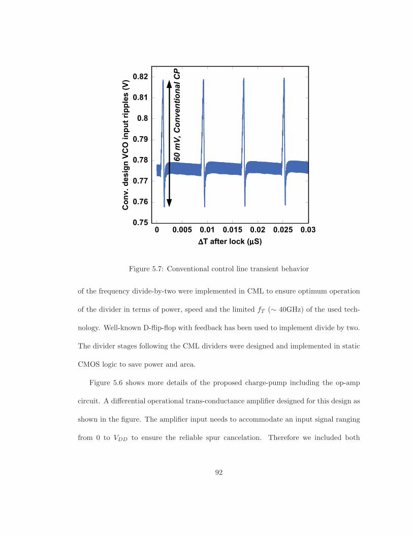
0.75
0.76
0.77
0.78
0.79
0.8
0.81
0.82
0 0.005 0.01 0.015 0.02 0.025 0.03
Con
v. d
esig
n VC
O in
put r
ippl
es (V
)
ΔΔΔΔT after lock (μμμμS)
Figure 5.7: Conventional control line transient behavior
of the frequency divide-by-two were implemented in CML to ensure optimum operation
of the divider in terms of power, speed and the limited fT (∼ 40GHz) of the used tech-
nology. Well-known D-flip-flop with feedback has been used to implement divide by two.
The divider stages following the CML dividers were designed and implemented in static
CMOS logic to save power and area.
Figure 5.6 shows more details of the proposed charge-pump including the op-amp
circuit. A differential operational trans-conductance amplifier designed for this design as
shown in the figure. The amplifier input needs to accommodate an input signal ranging
from 0 to VDD to ensure the reliable spur cancelation. Therefore we included both
92

0.75
0.76
0.77
0.78
0.79
0.8
0.81
0.82
0 0.005 0.01 0.015 0.02 0.025 0.03
Prop
osed
des
ign
VCO
inpu
t rip
ple
(V)
ΔΔΔΔT after lock (μμμμS)
Figure 5.8: Proposed design control line transient behavior (3.5X reduction)
PMOS and NMOS devices at the input of the amplifier to ensure proper operation of
the proposed scheme over the entire voltage range. Figures 5.7 and 5.8 show closed-loop
Spectre circuit simulation results for both PLLs in locked condition, respectively. The
design was modified slightly to ensure the simulations includ mismatch in the IUp and
IDown currents that are likely to occur in real fabricated design. As shown in the figures,
the disturbance on the control line was reduced from 60 mV to 17 mV in the proposed
charge-pump, a factor of 3.5X, in comparison to a conventional charge pump.
93

5.5 Experimental Results
To further validate the proposed design, both synthesizers were fabricated in a 0.18-μm
CMOS technology. All of the signals from the prototype chip except the buffered outputs
of synthesizer were wire-bonded, microwave probes were used to capture the PLL out-
put. Figure 5.9 shows the loop transient behavior of the proposed design along with the
corresponding zoomed-in spectrum captured with a HP E4407B spectrum analyzer. The
measured settling time was about 2.2 μs, which compares well with simulation results.
Next, the reference frequency was varied over the lock range (113MHz to 119.5MHz) of
the two designs and spur levels for both synthesizers were measured. The best improve-
ment in spur suppression was >22 dB as shown in Figure 5.10. As can been seen in
this figure the amount of spur suppression decreases whenever the reference frequency
is moved away from 117.5MHz. This is unfortunately mostly due to a layout error. VB1
could not be adjusted within the lock range and therefore the performance improvement
was limited. Our simulation suggest that fixing this problem can reduce the spur levels
to <-70 dBc.
Next, we show the spur levels for the two designs measured with a reference frequency
of 118 MHz in Figure 5.11 corresponding to the results plotted in Figure 5.10. The
proposed synthesizer core consumed 33.3 mW from a 1.8 V power supply. The power
consumption for the core plus drivers and 50-ohm output buffer was 57.6 mW. The
power consumption of the op-amp is minimal (≈ 4%) at 2.3 mW. The proposed charge-
pump design has a phase noise that is 4 dBc/Hz higher than the conventional design
94

0
0.2
0.4
0.6
0.8
1
1.2
1.4
1.6
0 0.8 1.6 2.4 3.2 4 4.8 5.6
Con
trol
Vol
tage
(V)
T im e (μμμμS)
Figure 5.9: Measured transient response and output spectrum for the proposed design
in lock. tsettling=2.2μs, flock= 5.76GHz
95
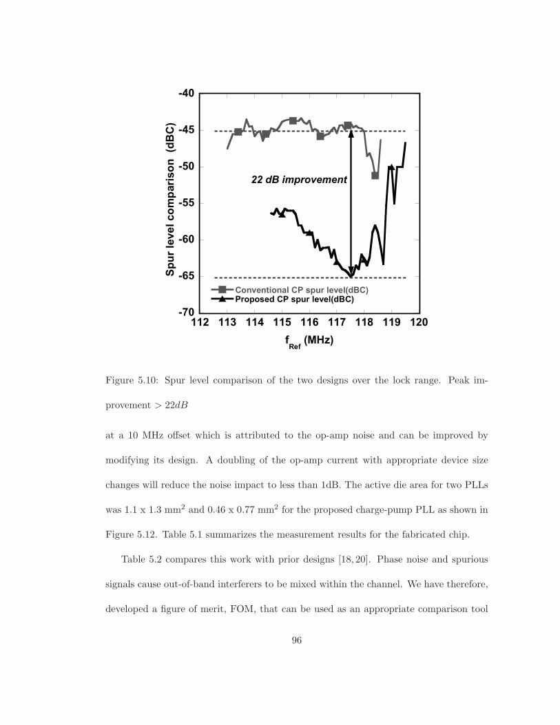
-70
-65
-60
-55
-50
-45
-40
112 113 114 115 116 117 118 119 120
Conventional CP spur level(dBC)Proposed CP spur level(dBC)
Spur
leve
l com
paris
on (
dBC
)
fRef
(MHz)
Figure 5.10: Spur level comparison of the two designs over the lock range. Peak im-
provement > 22dB
at a 10 MHz offset which is attributed to the op-amp noise and can be improved by
modifying its design. A doubling of the op-amp current with appropriate device size
changes will reduce the noise impact to less than 1dB. The active die area for two PLLs
was 1.1 x 1.3 mm2 and 0.46 x 0.77 mm2 for the proposed charge-pump PLL as shown in
Figure 5.12. Table 5.1 summarizes the measurement results for the fabricated chip.
Table 5.2 compares this work with prior designs [18, 20]. Phase noise and spurious
signals cause out-of-band interferers to be mixed within the channel. We have therefore,
developed a figure of merit, FOM, that can be used as an appropriate comparison tool
96

Figure 5.11: Measured output spectrum of conventional design (a) and proposed designs
(b) at fRef = 118 MHz
97

Figure 5.12: Microphotograph of the PLLs in a 0.18μm CMOS technology.
Figure 5.13: ITRS supply voltage roadmap for CMOS
98

Table 5.1: Summary of measurement results
Technology 180nm CMOS Conventional Proposed
Total circuit area 1.43mm2 charge-pump charge-pump
Spur level (fREF = 118.4MHz) -51dBc -58dBc
Spur level (fREF = 117.5MHz) -44dBc -66dBc
Power (including all drivers) 31.0 mW 33.3 mW
Phase noise @ 10MHz -125dBc/Hz -121dBc/Hz
of various wireless designs. This FOM is derived by summing the 1Hz bandwidth phase
noise normalized to a 10MHz offset with the spurious tones at the reference frequency.
An additional correction factor for loop-bandwidth/fRef is added since various designs
use different bandwidth. The proposed design has a higher loop-bandwidth/fRef ratio
(≈1/10 ) as opposed to the designs in [18,20] (≈1/36) resulting in a larger ripple voltage
for the same current impulse from the charge-pump. Therefore, there is a need for a
correction factor of 20log(36/10) for the spur levels in [18,20] to have a fair comparison.
The VCO power for all the designs are approximately equal and has been eliminated
from the FOM for clarity. Clearly, no single FOM can capture all the possible design
tradeoffs, however, this FOM is a good metric for wireless systems. As seen in the table,
our design has the best performance FOM, lowest complexity and can be designed for
future low voltage technologies. The supply voltage trends for CMOS technologies from
ITRS is shown in Figure 5.13. Our design can be realized in more advanced technologies
99

Table 5.2: Performance comparison of PLLs with improved charge-pump Circuits
Freq.
GHz
Spur
dBc
Phase-noise
dBc/Hz
Power
mW
fRef
BW FOM
dB
Design [18](0.24μm) 5.0 ≤-45 -101 @1MHz 32.0 36 -160.0
Design [20](0.24μm) 5.0 -70 -134 @22MHz 25.3 36 -184.5
Our design(0.18μm) 5.7 <-66 -121 @10MHz 33.3 10 -198.3
with smaller supply voltages.
5.6 Summary
Inherent delay and current mismatch in the combined phase detector/charge-pump, and
the coupling between charge-pump output and VCO control line leads to reference spurs.
In this chapter we proposed a single-ended charge-pump circuit to reduce the dynamic
disturbances on the control line. The design was verified using prototypes fabricated in
a 0.18-μm CMOS technology. Measurement results show a spur reduction of >22 dB,
in comparison to a conventional charge-pump based synthesizer. This design has a
better performance metric FOM, lower complexity and can be designed for lower supply
voltages.
100

Chapter 6
Conclusions, Research
Contribution & Future Directions
As presented throughout the thesis, the growing on-chip processor bandwidth predicted
by Moor’s law and the projected performance of I/O systems released by ITRS with the
performance gap shown in Figure 1.1 have spurred the demand for developing sophisti-
cated high-speed I/O transceivers in CMOS technologies [5]. Enormous channel losses
at high frequencies necessitate the use of channel equalization, which becomes more
power hungry and less efficient with increasing data rates. Crosstalk interferences from
neighboring channels become more pronounced relative to the received signal and nega-
tively affect the BER of the overall link as discussed in chapter 3. Chapter 3 proposes
PR equalization scheme which increases the link performance and SNR at the receiver
slicer/s input by reducing the signaling bandwidth and incorporating the crosstalk noise
101

into equalizer optimization problem. A transceiver architecture with transmit equalizer
and 1-tap DFE was described as a solution for parallel links with severe crosstalk sources.
Increased ISI components with growing data rates without improving the quality
of channel materials, adversely impact the performance of traditional edge-based CDR
circuits because of their sensitivity to the incoming data pattern. Also recovered clock
and therefore data quality is set by the transmit clock performance especially in source
synchronous systems. Chapter 4 presented a novel low-power pilot-based CDR which
was designed, fabricated and measured in a 5Gb/s fully differential receiver using 0.13μ
CMOS technology. The pilot-based CDR decouples the recovered clock performance
from channel ISI components with only a 5% amplitude overhead to transmitter while
recovering a clock with 1.6ps jitter rms while consuming only 11.75mA from a 1.5V
supply.
Transmit clock generated by a CP PLL suffer from reference side-band spur problem,
which deteriorates the clock jitter and phase noise performance in both wireless and
wireline applications. Chapter 5 introduces a reduced spur single-ended CP PLL, which
dynamically corrects the CP current to suppress side-band spurs. A 5.6GHz single-ended
CP PLL was designed, fabricated and measured in a 0.18μ CMOS technology. The side-
band spurs were suppressed by 22dB and consequently improved the generated clock
jitter performance.
102

Figure 6.1: Proposed phase adjustment with eye height monitoring and interpolators
6.1 Future Directions
6.1.1 Adaptive Phase Recovery for Pilot-Based CDR Scheme
As described in chapter 4, the combined data and pilot is subjected to channel frequency
response, which may have a different phase response for the narrow-band pilot signal ver-
sus the wide-band data. As described previously, the phase adjustment can be performed
by using a DLL at the transmitter and timing calibration cycles in bi-directional links
such as DDR3 and GDDR5 memory interfaces [46]. Figure 6.1 illustrates a proposed
phase adjustment circuit used in conjunction with pilot-based CDR scheme presented
in chapter 4. This scheme comprises of a cascade of several CML inverter delay cells,
here four stages with coarse tunable varactors at the output of each stage, a phase mixer
which selects two distinct phases from the delay cell chain and a phase interpolator which
103

adjusts the fine tuned sampling clock phase. This scheme use the two dimensional eye
monitoring technique presented in [45] to place the sampling clock in the optimum place
in eye diagram. The eye monitoring circuit measures a figure of merit representing the
maximum two dimensional eye opening over time and feeds back this information to the
state machine which intelligently changes the phase mixer outputs and phase interpolator
gain.
6.1.2 A Unified Pilot-Based CDR and PR Equalization I/O
Transceiver
PR equalization was shown to outperform traditional equalization schemes in the envi-
ronments where crosstalk is the dominant noise. It was shown that the proposed PR
equalization scheme is advantageous in terms of DFE loop timing convergence which is
a limiting factor in DFE circuit implementation. Also the proposed pilot-based CDR
circuit introduced in chapter 4 enables I/O systems to decouple the clock performance
from the incoming data pattern with a small amplitude overhead at the transmitter with-
out an additional need for a dedicated channel for the clock signal. These two powerful
features can be combined in an I/O transceiver to benefit from their distinct feature.
Figure 6.2 illustrates the proposed I/O transceiver to be designed and characterized.
The I/O transmitter shown in the figure uses a traditional transmit equalizer which
equalizes the channel response to an impulse, duobinary or PR11b based on the channel
characteristic. The output driver combines the equalized NRZ data with a low amplitude
pilot signal as described in section 4.3.6 of chapter 4. The receiver is similar to the PR
104

Figure 6.2: Unified pilot-based CDR and PR equalization scheme for I/O transceivers
equalization receive scheme described in chapter 3 and can be configured to use a double
threshold or single threshold slicer based on the channel loss values and characteristics.
The pilot tone frequency needs to be accordingly adjusted. The transmit pilot signal
frequency is equal to NRZ bit-rate for 2-PAM signaling which places the pilot signal at
the NRZ data notch. The pilot frequency is equal to bit-rate divide by two or fBitrate/2
when using the partial response equalization. The received equalized signal is a duobinary
signal after the first tap DFE cancelation when PR11b used. This received equalized signal
occupies only half of the bandwidth as compared to 2-PAM signaling [6, 7]. Therefore,
pilot-based CDR scheme benefits from this lower frequency, fBitrate/2, since the transmit
pilot tone is subjected to a much lower channel loss which further results in less voltage
overhead ofVpilot
VDataat the transmitter.
105

Appendix A
Partial Response MMSE
Optimization Problem
This appendix includes more detailed assumptions and simplifications required for under-
standing the solution to the optimization problem presented in Section 3.4 of chapter 3.
The following equations show the summary of the MMSE problem. Here x1 is the victim
line, xr’s for ∀r 2 ≤ r ≤ M are the dominant aggressor signals which contribute to n2(k)
(colored noise component) and n1(k) is white noise which has zero mean value and is
uncorrelated with respect to the transmit bit streams. The MMSE solution include the
transmit equalizer tap values, fopt(i) for ∀i −L ≤ i ≤ L and bopt which depends on the
channel response and optimum target response for PR equalization.
106
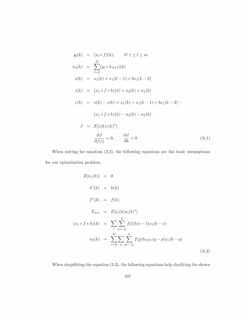
yl(k) = (xl ∗ f)(k), ∀l 1 ≤ l ≤ m
n2(k) =
M∑l=2
(yl ∗ hXTl)(k)
s(k) = x1(k) + x1(k − 1) + bx1(k − 2)
z(k) = (x1 ∗ f ∗ h)(k) + n2(k) + n1(k)
ε(k) = s(k)− z(k) = x1(k) + x1(k − 1) + bx1(k − 2)−
(x1 ∗ f ∗ h)(k)− n2(k)− n1(k)
J = E[ε(k)ε(k)∗]
∂J
∂f(i)= 0,
∂J
∂b= 0 (A.1)
When solving for equation (3.2), the following equations are the basic assumptions
for our optimization problem.
E[n1(k)] = 0
h∗(k) = h(k)
f∗(k) = f(k)
Exxi = E[xi(k)xi(k)∗]
(x1 ∗ f ∗ h)(k) =∑v
L∑l=−L
f(l)h(v − l)x1(k − v)
n2(k) =M∑r=2
∑q
L∑p=−L
f(p)hXTr(q − p)xr(k − q)
(A.2)
When simplifying the equation (3.3), the following equations help clarifying the shown
107

results in (3.4).
∂E
∂b[bx1(k − 2)(x1 ∗ f ∗ h)(k)] = Exx1
L∑p=−L
f(p)h(2− p)
∂E
∂fi[x1(k)(x1 ∗ f ∗ h)(k)] = Exx1h(−i)
∂E
∂fi[x1(k − 1)(x1 ∗ f ∗ h)(k)] = Exx1h(1− i)
∂E
∂fi[(x1 ∗ f ∗ h)(k)(x1 ∗ f ∗ h)∗(k)] = Exx1
∑v
L∑p=−L
f(p)h(v)h(v + p− i)
∂E
∂fi
[M∑r=2
(xr ∗ f ∗ hXTr)(k)M∑r=2
(xr ∗ f ∗ hXTr)(k)∗]=
Exx1
∑v
L∑p=−L
f(p)h(v)h(v + p− i)
(A.3)
108

Bibliography
[1] A.J. Viterbi, “Phase-Locked Loop Dynamics in the presence of noise by Fokker-
Planck Techniques,” Proceedings of the IEEE, pp. 1737–1753, Dec. 1963.
[2] K.-J. Sham, M. R. Ahmadi, S. Bommalingaiahnapallya, G. Talbot, and R. Harjani,
“FEXT crosstalk cancellation for high-speed serial link design,” Proc. IEEE Custom
Integrated Circuits Conf., pp. 405–408, Sept. 2006.
[3] B. Razavi, Design of Integrated Circuits for Optical Communications, McGraw-Hill,
New York, NY, 2003.
[4] W. Dally and J. Poulton, Digital Systems Engineering, Cambridge University Press,
New York, NY, 1998.
[5] International Technology Roadmap for Semiconductors, “(ITRS) 2007 Edition Ex-
ecutive Summary,” 2007.
[6] John G. Proakis, Digital Communications (Fourth Edition), McGraw-Hill, New
York, NY, 2001.
109

[7] R.W. Lucky, J. Salz, and JR. E.J. Weldon, Principles of Data Communication,
McGraw-Hill, New York, NY, 1968.
[8] V. Stojanovic, A. Ho, B. Garlepp, F. Chen, J. Wei, E. Alon, C. Werner, J. Zerbe,
and M.A. Horowitz, “Adpative Equalization and Data Recovery in a Dual-Mode
(PAM2/4) Serial Link Transceiver,” IEEE Symposium on VLSI Circuits, pp. 348–
351, June 2004.
[9] J. Ren, H. Lee, Q. Lin, B. Leibowitz, E. Chen, D. Oh, F. Lambrecht, V Stojanovi,
C. Yang, and J. Zerbe, “Precursor isi reduction in high-speed i/o,” IEEE Symposium
on VLSI Circuits, pp. 134–135, June 2007.
[10] http://www.hypertransport.org/, “The HyperTransport Consortium,” .
[11] http://www.t10.org/, “SCSI Storage Interfaces,” .
[12] J. Buckwalter and A. Hajimiri, “Cancellation of crosstalk-induced jitter,” IEEE
Journal of Solid-State Circuits, vol. 41, no. 3, pp. 621–631, March 2006.
[13] Agilent Technologies, “Jitter Analysis: The dual-Dirac Model, RJ/DJ, and Q-
Scale,” .
[14] James Franklin Buckwalter, Deterministic Jitter in Broadband Communication,
Ph.D. thesis, California Institute of Technology, January 2006.
110
[15] F. Lambrecht, Q. Lin, S. Chang, D. Oh, C. Yuan, and V. Stojanovic, “Accurate
System Voltage and Timing Margin Simulation in CDR Based High Speed Designs,”
IEEE Transactions on Advanced Packaging, pp. 772–730, November 2008.
[16] Huang Chunxing and Sanjeev Gupta, “Statistical Eye Simulation and Modeling
High-Speed Serial Links,” February 2007.
[17] Keshab K. Parhi, “High-speed architectures for algorithms with quantizer loops,”
IEEE International Symposium on Circuits and Systems, pp. 2357–2360, May 1990.
[18] H. R. Rategh, H. Samavati, and T.H. Lee, “A 5GHz, 32mW CMOS Frequency
Synthesizer With an Injection Locked Frequency Divider,” IEEE Symposium on
VLSI Circuits, pp. 113–116, June 1999.
[19] T. Lee and B. Razavi, “A Stabilization Technique for Phase-Locked Frequency
Synthesizers,” IEEE Journal Solid-State Circuits, vol. 38, no. 6, pp. 888–894, June
2003.
[20] H. Samavati, H. R. Rategh, and T.H. Lee, “A Fully-integrated 5 GHz CMOS
Wireless-LAN Receiver,” International Solid State Circuit Conference, pp. 208–
209, February 2001.
[21] J. Zerbe, C. Werne, V. Stojanovic, F. Chen, J. Wei, G. Tsang, D. Kim,
W. Stonecypher, A. Ho, T. Thrush, R. Kollipara, M. Horowitz, and K. Don-
nelly, “Equalization and clock recovery for a 2.5-10Gb/s 2-PAM/4-PAM backplane
transceiver cell,” IEEE J. Solid-State Circuits, vol. 38, pp. 2121–2130, Dec. 2003.
111

[22] V. Stojanovic, A. Amirkhany, and M. Horowitz, “Optimal linear precoding with
theoretical and practical data rates in high-speed serial-link backplane communi-
cation,” IEEE International Conference on Communications, pp. 2799–2806, June
2004.
[23] K. Yamaguchi, K. Sunaga, S. Kaeriyama, T. Nedachi, M. Takamiya, K. Nose,
Y. Nakagawa, M. Sugawara, and M. Fukaishi, “12Gb/s Duobinary Signaling with 2x
Oversampled Edge Equalization,” IEEE Int. Solid-State Circuits Conf. Dig. Tech.
Papers, pp. 70–585, February 2005.
[24] J.H. Sinsky, M. Duelk, and A. Adamiecki, “High-speed electrical backplane trans-
mission using duobinary signaling,” IEEE Transactions on Microwave Theory and
Tech., pp. 152–160, January 2005.
[25] Jaekyun Moon, “The role of sp in data-storage systems,” IEEE Signal Processing
Magazine, vol. 15, pp. 54–72, July 1998.
[26] J. Moon and W. Zeng, “Equalization for maximum likelihood detectors,” IEEE
Transactions on Magnetics, vol. 31, pp. 1083–1088, March 1995.
[27] M.R. Ahmadi, J. Moon, and R. Harjani, “Constrained Partial Response Receivers
for High-Speed Links,” IEEE Transactions on Circuits and Systems-II Express
Briefs, pp. 1006–1010, October 2008.
[28] M. Thomlinson, “New automatic equalizer employing modulo arithmetic,” Elec-
tronics Letters, vol. 7, pp. 138–139, March 1971.
112
[29] Mahmoud Reza Ahmadi, Amir Amirkhany, and Ramesh Harjani, “A 5Gbps 0.13μm
CMOS Pilot-Based Clock and Data Recovery Scheme for High-Speed Links,” Proc.
IEEE Custom Integrated Circuits Conf., pp. 557–560, Sept. 2009.
[30] A. Amirkhany, A. Abbasfar, V. Stojanovic, and M.A. Horowitz, “Analog Multi-
Tone Signaling for High-Speed Backplane Electrical Links,” IEEE Global Telecom-
munications Conference, pp. 1–6, Nov.-Dec. 2006.
[31] A. Amirkhany, A. Abbasfar, J. Savoj, R.T. Kollipara, V. Stojanovic, and M.A.
Horowitz, “A 24 Gb/s Software Programmable Multi-Channel Transmitter,” IEEE
Symposium on VLSI Circuits, pp. 38–39, June 2007.
[32] B.S. Leibowitz, J. Kizer, Haechang Lee, F. Chen, A. Ho, M. Jeeradit, A. Bansal,
T. Greer, S. Li, R. Farjad-Rad, W. Stonecypher, Y. Frans, B. Daly, F. Heaton,
B.W. Gariepp, C.W. Werner, Nhat Nguyen, V. Stojanovic, and J.L. Zerbe, “A
7.5Gb/s 10-Tap DFE Receiver with First Tap Partial Response, Spectrally Gated
Adaptation, and 2nd-Order Data-Filtered CDR,” IEEE Int. Solid-State Circuits
Conf. Dig. Tech. Papers, pp. 228–229, February 2007.
[33] J.-H.C. Zhan, J.S. Duster, and K.T. Kornegay, “Full-rate injection-locked 10.3Gb/s
clock and data recovery circuit in a 45GHz-fT SiGe process,” Proc. IEEE Custom
Integrated Circuits Conf., pp. 557–560, Sept. 2005.
[34] S. Erba and et al, “A 10Gb/s receiver with linear backplane equalization and
mixer-based self-aligned CDR,” Proc. IEEE Custom Integrated Circuits Conf., pp.
113
559–562, Sept. 2008.
[35] Wei-Hung Chen, Guang-Kaai Dehang, Jong-Woei Chen, and Shen-Iuan Liu, “A
CMOS 400-Mb/s serial link for AS-memory systems using a PWM scheme,” IEEE
J. Solid-State Circuits, vol. 36, no. 10, pp. 1498–1505, October 2001.
[36] C. Svensson and J. Yuan, “A three-level asynchronous protocol for a differential
two-wire communication link,” IEEE J. Solid-State Circuits, vol. 29, no. 9, pp.
1129–1132, September 1994.
[37] G. W. den Besten, “Embedded low-cost 1.2 Gb/s inter-IC serial data link in 0.35um
CMOS,” IEEE Int. Solid-State Circuits Conf. Dig. Tech. Papers, pp. 282–283,
February 2000.
[38] Mahmoud Reza Ahmadi, Amir Amirkhany, and Ramesh Harjani, “A 5Gbps 0.13μm
CMOS Pilot-Based Clock and Data Recovery Scheme for High-Speed Links,” IEEE
Journal of Solid-State Circuits, August 2010.
[39] A. Abbasfar, A. Amirkhany, and B. W. Garlepp, “Signaling with Superimposed
Clock and Data Signals,” United States Patent No. 0297213A1, December 2008.
[40] Hamid R. Rategh and Thomas H. Lee, “Superharmonic Injection-Locked Frre-
quency Dividers,” IEEE J. Solid-State Circuits, vol. 34, no. 6, pp. 813–821, June
1999.
[41] B. Razavi, “A study of injection locking and pulling in oscillators,” IEEE J. Solid-
State Circuits, vol. 39, no. 9, pp. 1415–1424, September 2004.
114

[42] N. Lanka, S. Patnaik, and R. Harjani, “Understanding the Transient Behavior of
Injection Locked LC Oscillators,” Proc. IEEE Custom Integrated Circuits Conf.,
pp. 559–562, Sept. 2007.
[43] Thomas H. Lee, The Design of CMOS Radio-Frequency Integrated Circuits:Second
Edition, Cambridge University Press, New York, NY, 1998.
[44] Rongtai Wang and Ramesh Harjani, “Partial Positive Feedback for Gain Enhance-
ment of Low-Power CMOS OTAs,” Low-Voltage Low-Power Analog Integrated Cir-
cuits, vol. 8, no. 1, pp. 21–35, July 1995.
[45] B. Analui, A. Rylyakov, S. Rylov, M. Meghelli, and A. Hajimiri, “A 10-Gb/s Two-
Dimensional Eye-Opening Monitor in 0.13-μm Standard CMOS,” IEEE Journal of
Solid-State Circuits, vol. 40, no. 12, pp. 2689–2699, December 2005.
[46] http://www.jedec.org/, “JEDEC Solid State Technology Association,” .
[47] S. Lee, Y. Kim, H. Ha, Y. Seo, H. Park, and J. Sim, “A 650Mb/s-to-8Gb/s Ref-
erenceless CDR Circuit with Automatic Acquisition of Data Rate,” IEEE Int.
Solid-State Circuits Conf. Dig. Tech. Papers, pp. 184–185, Feb. 2009.
[48] A. Hajimiri and T.H. Lee, “Oscillator Phase Noise: A Tutorial,” IEEE Journal
Solid-State Circuits, pp. 326–336, March 2000.
115