future trend in memory device - koreatest.or.kr · sk hynix. 1/44 where we are? 2/44 everything is...
TRANSCRIPT

Future Trend in Memory Device
Cho Jeong Ho
2012.06.27
SK hynix

1/44
Where we are?
2/44
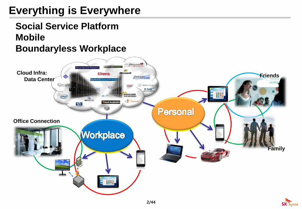
Everything is Everywhere
Cloud Infra:
Data Center
Family
Friends
Office Connection
Social Service Platform
Mobile
Boundaryless Workplace

3/44
Wearable Computer
Nano-Technology + Bio Technology
Natural User Interface : Analog, Gesture, Voice
4/44
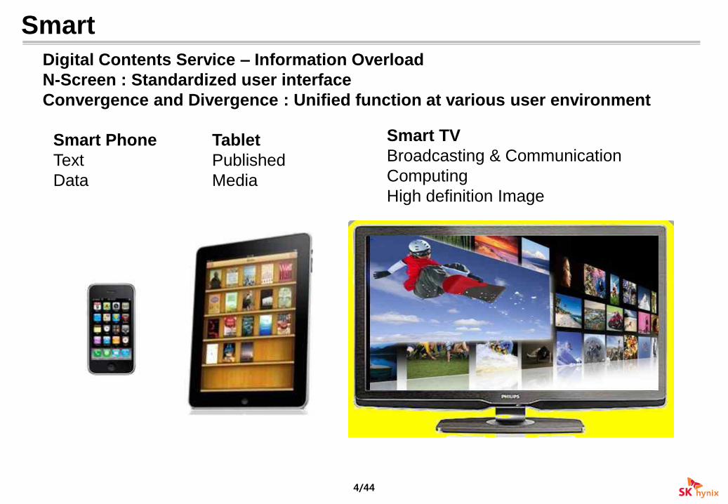
Smart
Smart Phone
Text
Data
Tablet
Published
Media
Smart TV
Broadcasting & Communication
Computing
High definition Image
Digital Contents Service – Information Overload
N-Screen : Standardized user interface
Convergence and Divergence : Unified function at various user environment

5/44
Big Data
3D Graphic
3D Game
3D Map
WeatherGeological
Medical Service
Real time unstructured Big Data processing
High capacity network
Visualization
6/44
- Cloud Computing
- Big Data
- Mobile
- Visualization
- Smart
- Natural User Interface
- Convergence & Divergence
- Network- Digital Contents
IT Trends

7/44
Memory requirement

8/44
Cloud Computing & Big Data
Memory Centric System
High Capacity & Bandwidth Memory
SCM (Storage Class Memory)Source: IDF Beijing (Apr`12)
Big data
Traditional
Data
Memory requirement
3D & High Definition
Visualization
Frame Buffer Size & GPU multi-Core
Higher Bandwidth/Density Memory
Network
Fast Growing Network Traffic High Bandwidth Memory
Multi Tera-Bit Systems
9/44
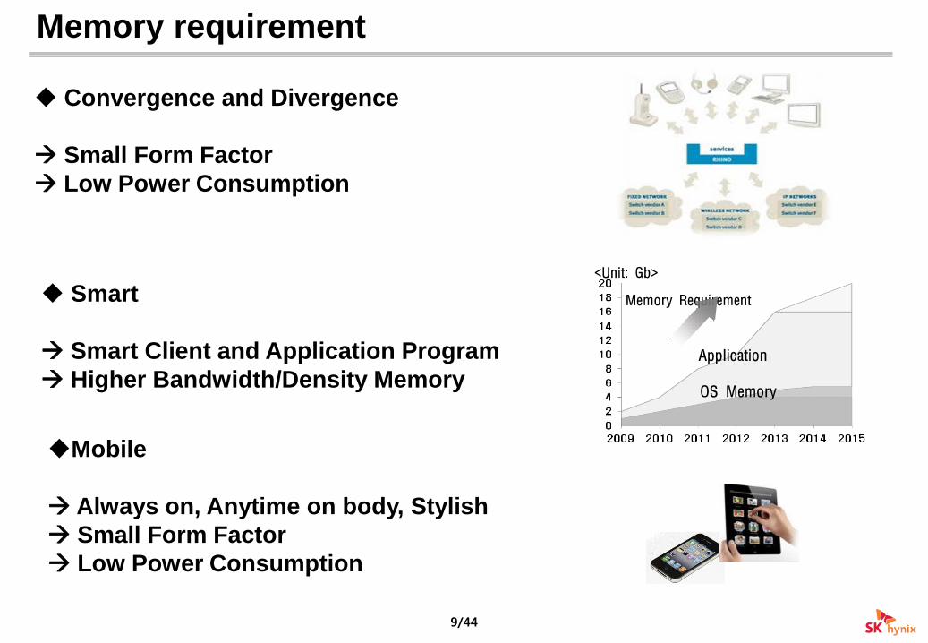
Convergence and Divergence
Small Form Factor
Low Power Consumption
Memory requirement
Smart
Smart Client and Application Program
Higher Bandwidth/Density Memory
Memory Requirement
OS Memory
Application
<Unit: Gb>
Mobile
Always on, Anytime on body, Stylish
Small Form Factor
Low Power Consumption

10/44
Memory Requirement
IT Trends HighCapacity
HighBandwidth
LowPower
SmallForm Factor
Cloud & Big Data High High High Middle
Visualization High High
Network High Middle Middle
Convergence & Divergence
Middle High High High
Smart High High
Mobile High High
Rating of Memory requirements to cope with IT trends

11/44
Memory Barrier

12/44
Power
Limited System Power Budget
-> Regulation for Standby power + Operating Power
-> Demands Revolutionary Approach
Energy StarIn 1992 the US Environmental Protection Agency (EPA) introduced ENERGY STAR as a voluntary labeling program
designed to identify and promote energy-efficient products to reduce greenhouse gas emissions. Computers and
monitors were the first labeled products. Through 1995, EPA expanded the label to additional office equipment
products and residential heating and cooling equipment. In 1996, EPA partnered with the US Department of Energy for
particular product categories. The ENERGY STAR label is now on major appliances, office equipment, lighting, home
electronics, and more.
Version 5.0 Energy Efficiency Requirements
Product Type Requirements
Desktops, Integrated Com
puters
•Category A: <= 148.0 kWh
•Category B: <= 175.0 kWh
•Category C: <= 209.0 kWh
•Category D: <= 234.0 kWh
Source : www.energystar.gov

13/44
Performance
Speed up per pin Wide memory IO
LPDDR3
2009 2010 2011 2012
Computingmemory
Graphic memory
Mobile memory
2005 2006 2007 2008
DDR3
GDDR3 GDDR5
DDR4
2013 2014
Next ?

14/44
Capacity
Limits of process technology scaling
Stacking Solution
1
10
100
1000
10000
100000
1992 2002 2012 2022
4Mb
16Gb*log scale
256Mb
4Gb
x1000
Monolithic device density

15/44
Form-Factor
Iphone3G12.3mm
Galaxy S9.9mm Iphone4
9.3mmXperia Arc8.7mm
Galaxy SⅡ8.49mm
2009 2010 2011
Smartphone Thickness Trend
5.4mm
Scaling & Thin wafer processing

16/44
Memory Evolution

17/44
Memory Evolution
Process technology scaling
1Xnm? 2xnm?
Next Generation Transistor
Multi-gate, FinFET, 3D transistor, Fully depleted SOI,
High-K/Metal Gate, Air gab
3D chip stack based on TSV
Speed per pin -> Number of IOs
Next Generation Memory
PRAM, MRAM, ReRAM
High Capacity and Bandwidth, Small F/F, Low Power Requirements

18/44
Next Generation Transter
FinFET 3D tri-gate transistor
Fully depleted SOI

19/44
3D Chip Stack Based on TSV
Packaging Platform
Source: Yole Development, Semicon Korea 2008

20/44
SOC or Interposer
3D Chip Stack Based on TSV
TSV - Through Silicon-Via
Memory
Memory
Memory
Memory
SOC or Interposer
Memory
Memory
Memory
Memory
Interface Chip
Cases of 3D Memory Stack
Vertical electrical connection passing completely through a silicon
wafer or die.
Interface Chip
Memory
Memory
Memory
Memory
SOC or Interposer

21/44
3D Chip Stack Based on TSV
Temporary Bonding/De-bonding
Wafer Thinning
Carrier
Wafer
Back Side Bump Structure
Interconnection
Front Side Bump
Gap Filling(NCP, NCF, MUF)
TSV Via (Via Middle)
Wafer Mold
Bumping Temporary Bond & De-bonding Thinning & Stacking
Critical Process of 3D Stack Memory

22/44
3D Chip Stack Based on TSV
X4 2Rank 16GB DIMM8Gb DDP or TSV 5MCP 18ea
X4 2Rank 16GB DIMMSDP 36ea
Pow
er
Case T
em
p.
SI -
marg
in
Comparison
-8Gb 5MCP
-8Gb DDP
-4Gb SDP
vs.

23/44
3D Chip Stack Based on TSV
High Bandwidth
- Speed per pin
- Massive number of IOs
Features GDDR5 HBM WIO
Density 2Gb 2Gb 4Gb
Speed per pin 6Gbps 1Gbps 200Mbps
Channel 1 2 4
Bank 16 8 / ch 4 / ch
DQs 32 256 512
# of Stack 1 4 4
DQs aft Stack 32 1024 512
Bandwidth 24GB/s 128GB/s 12.8MB/s

24/44
Power SavingHigh Band Width
Performance Cost
ReliabilityForm-factor
Additional ProcessLow Stacking Yield
Delivery
Small SizeHigh Density
Micro JoiningCu Contamination
Thin Die
3D Chip Stack Based on TSV
Pros and Cons

25/44
3D Chip Stack Based on TSV
Multi-wafer burn-in for reliability and yield
Testing of VIA defects at wafer level
Probing on the u-bump for mission mode test
KGSD test (Wafer or Package)
Memory BIST, BIRA, BISR for memory test in SiP
Test Challenges

26/44
Next Generation Memory
Requirements for Next Generation Memory
Maintain same memory budget in a system
Cost of new material, Scalable for Generations
Meet performance trends
Backward compatible interface
DDR4 like?
More Moore and/or More than Moore
Geometrical Scaling / Extends the benefits of Moore’s Law
Green Product
Healthy, Safe, Environment-friendly

27/44
Next Generation Memory
Promising Candidates
PCRAM(Phase-Change RAM)
- Non-Volatile
- Medium Performance
- Storage Class Memory
STT-MRAM(Spin Transfer Torque RAM)
- Non-Volatile
- DRAM and NAND alternatives
- Expensive
ReRAM(Resistive RAM)
- Non-Volatile
- NAND alternatives
- High Density

28/44
Next Generation Memory
PCRAM
Phase-Change Material
- More than 2 phases with different properties
- Repeatedly switchable between phases
Amorphous phase
- High electrical resistivity
- Low optical reflectivity
Crystalline phase
- Low electrical resistivity
- High optical reflectivity
In 1960s, Phase-Change material was demonstrated.
In 1990s, discovering of fast crystallization materials draws industrial attention.
29/44
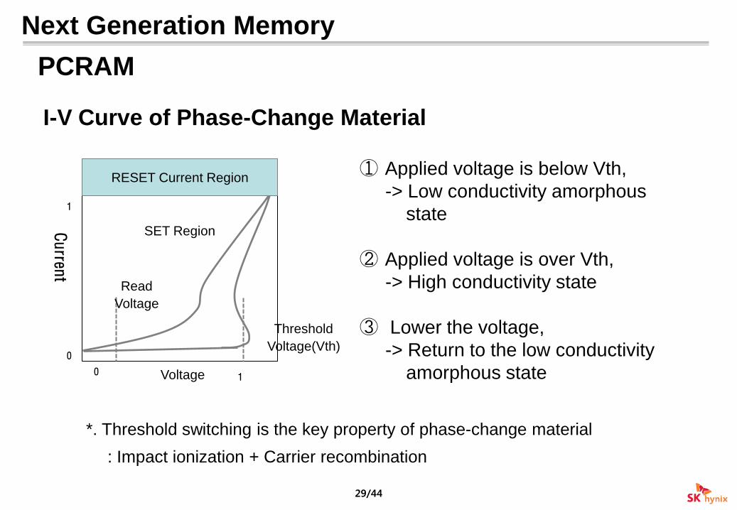
Next Generation Memory
PCRAM
RESET Current Region
SET RegionCurren
t
Voltage
0
01
1
Threshold
Voltage(Vth)
Read
Voltage
I-V Curve of Phase-Change Material
① Applied voltage is below Vth,
-> Low conductivity amorphous
state
② Applied voltage is over Vth,
-> High conductivity state
③ Lower the voltage,
-> Return to the low conductivity
amorphous state
*. Threshold switching is the key property of phase-change material
: Impact ionization + Carrier recombination

30/44
Next Generation Memory
PCRAM
Cell Structure
1) Contact minimized cell : Minimize the size of electrical contact
Low heat loss (heat concentrates on the small contact spot)
2) Volume minimized cell : Minimize the size of Phase-Change material
Low RESET current, High Endurance
Bit Line
Word Line
Phase Change Material
Contact
Access Device
Contact Minimized Cell
Bit Line
Word Line
Phase Change Material
Confined
VolumeAccess Device
Volume Minimized Cell

31/44
Next Generation Memory
PCRAM
Bit Line
Word Line
CrystallizationAccess Device
Phase-Change Material
Cell OperationRESET : Amorphous highly resistive state
High power pulse current
Temp. > T-melting
SET : Crystalline highly conductive state
Moderate power and long duration pulse current
T-crystallization < Temp. < T-melting
READ : Sensing the resistance difference between the two state
Very low power current
RE
SE
T/S
ET
Cu
rren
t
Time
0
0 1
1 RESET
SET
32/44
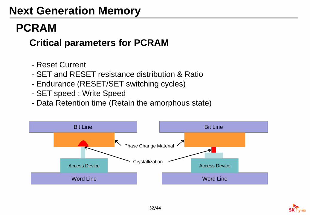
Next Generation Memory
PCRAM
Critical parameters for PCRAM
- Reset Current
- SET and RESET resistance distribution & Ratio
- Endurance (RESET/SET switching cycles)
- SET speed : Write Speed
- Data Retention time (Retain the amorphous state)
Bit Line
Word Line
CrystallizationAccess Device
Bit Line
Word Line
Access Device
Phase Change Material
33/44
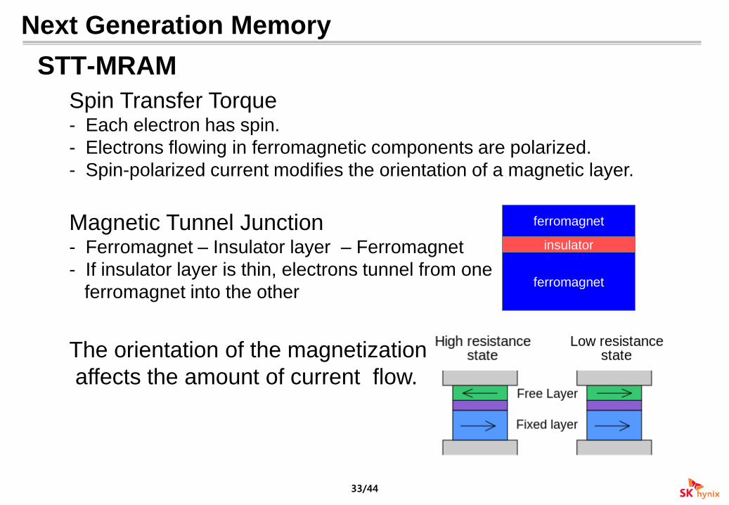
Next Generation Memory
STT-MRAM
Spin Transfer Torque- Each electron has spin.
- Electrons flowing in ferromagnetic components are polarized.
- Spin-polarized current modifies the orientation of a magnetic layer.
Magnetic Tunnel Junction- Ferromagnet – Insulator layer – Ferromagnet
- If insulator layer is thin, electrons tunnel from one
ferromagnet into the other
ferromagnet
ferromagnet
insulator
The orientation of the magnetization
affects the amount of current flow.

34/44
Next Generation Memory
STT-MRAM
Cell Structure
- MTJ (Magnetic Tunnel Junction)
- Thick Ferromagnetic Layer (Fixed Layer)
- Thin Ferromagnetic Layer (Free Layer)
- Thin Insulator Layer (Tunnel Barrier)
Write Word line
Bypass
Bit Line
MRAM
MTJ
Gate
Bit Line
STT-MRAM
DrainSource
MTJ

35/44
Next Generation Memory
STT-MRAM
Cell Operation- Conventional MRAM
Magnetic field generated by Write Word Line
- STT-MRAM
Spin transfer effect by spin-polarized current flowing through MTJ
Write Word line
Bypass
Bit Line
MRAM
MTJ
Gate
Bit Line
STT-MRAM
DrainSource
MTJ
Fixed Orientation
Orientation switching between parallel and anti-parallel

36/44
Next Generation Memory
STT-MRAM
Critical parameters for STT-MRAM
- TMR (Tunnel Magnetoresistance)
Read margin & speed
- Write current density
Write current scales down with cell size
- Vbd : MTJ breakdown voltage
Life time, endurance
- Thermal stability
Data retention

37/44
Next Generation Memory
ReRAM
Negative differential resistance (NDR)
- Increased voltage/current result in radical decrease of
current/voltage
CCNR (Current Control NDR)
VCNR (Voltage Control NDR)
Switching Mechanism
- Conducting Filament model
Metallic filament
- Electronic Switching model
Charge trap / de-trap etc.
38/44
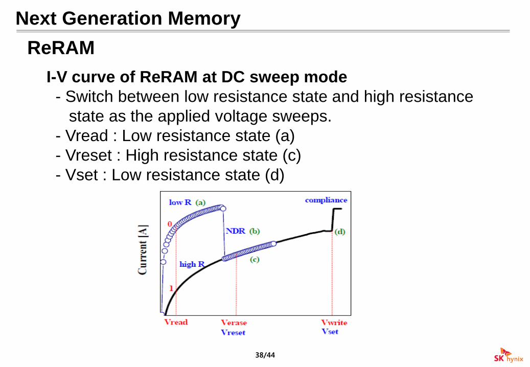
Next Generation Memory
ReRAM
I-V curve of ReRAM at DC sweep mode
- Switch between low resistance state and high resistance
state as the applied voltage sweeps.
- Vread : Low resistance state (a)
- Vreset : High resistance state (c)
- Vset : Low resistance state (d)

39/44
Next Generation Memory
ReRAM
Cell Structure- Resistive Element
MIM (Metal / Insulator / Metal)
- Cross Point cell
- 1 Diode 1 Resistor
- 1 TR 1 Resistor
Word Line
Bit line
Word Line
Bit line
Resistive element
Diode + MIM element
Bit Line
Source Line
Cross Point Cell 1D 1R1T 1R

40/44
Next Generation Memory
ReRAM
Cell Operation- RESET
High voltage from Word line to Bit line
High resistive state
- SET
High voltage from Bit line to Word line
Low resistive state
- READ
Low voltage from Bit line to Word line
Non-destructive operation
Vset2
Vset1
Vreset1
Vreset2
Vread1
Vread2

41/44
Next Generation Memory
ReRAM
Critical Parameters for ReRAM
- Forming Voltage
- SET and RESET resistance distribution & Ratio
- Endurance (RESET/SET switching cycles)
- Sneak Current
SET Current
Sneak Current
42/44
Next Generation Memory
Test challenges of NGM
• DDR4-like or DDR4 interface eases ATE options
But
• Inexperienced Material and Geometry behavior
• Unknown Yield and Reliability model
• Timely Test Baseline and Quality Control
are challenging issues.
In-depth fault modeling and studies for the behaviors of
faults are required.

43/44
Summary
Traditional Memory Trends are
low power, high bandwidth, high density, small form factor
3D memory technology based on TSV is emerging
Requirements for Next Generation Memory are
- Maintain same memory budget in a system
Cost of new material, Scalable for Generations
- Meet performance trends
- Backward compatible interface
DDR4 like?
- More Moore and/or More than Moore
Geometrical Scaling / Extends the benefits of Moore’s Law
- Green Product
Healthy, Safe, Environment-Friendly

44/44
Thanks