g a manufacturing filtronic ramps phemts for …iopp.fileburst.com/cs/cs_11_10.pdf · /pw o %fd...
TRANSCRIPT
Filtronic ramps PHEMTs forhandset transmit modules
Showa Denko togrow LED capacity
Cree details latestprogress with SiC
A look insideChinese handsets
ALSO INSIDE
GAAS MANUFACTURING
November 2005 Volume 11 Number 10


NOVEMBER 2005 VOLUME 11 NUMBER 10
Cree unveiled its high-power thyristors at thisyear’s ICSCRM meeting in Pittsburgh. p19
Canada’s photonic start-ups benefit from anational III-V chip production center. p16
The solid-state lighting community is urgedto tackle industry infrastructure issues. p8
5 Headline News Showa Denko plans LED capacity ramp...Handset juggernaut heads toward 800 m...RFMD tipped to win ‘arms race’as it increases dollar content
7 GaAs & Wireless News French foundry in MMIC research collaboration...Hittite profits rise after impressive quarter...450 MHz may boost low-cost handsets...Military sales help to get TriQuint back on track
8 LED News Infrastructure change is vital for SSLrevolution...Cree breaks revenue barrier of $100 m...Huga and LG Innotek ramp chip production...Nichia reveals Kirameki devices for headlamps...LED wafer scriber meets 4 inch capability
10 Opto News DVD camps continue war of words as format struggle enters critical period...UK team to develop terahertz imager
11 Fiber News Princeton plans to launch cryptography detector...Bookham’s figures reveal cash boost
12 Wide Bandgap News Oki’s GaN HEMT delivers record transconductance...SatCon selects SiC for power converter
31 M&E News Cautious Aixtron drops sales guidance...Optimistic AXT reduces staff at Fremont facility...Veeco, Riber say worst is over...In brief
COMPOUND SEMICONDUCTOR NOVEMBER 2005 1
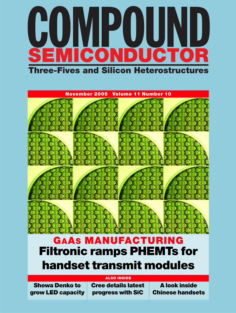
On the cover: Filtronic’s rapid ramp in the manufacture of PHEMTs for antenna switches is driving its 6 inch GaAs production to profitability. The cover imageshows PHEMT-based MMICs for cellular base stations manufactured on the company’s production line (image courtesy of Filtronic).
NEWS
22 Substrates and Epiwafers Suppliers Guide
32 Product Showcase
ADVERTISING SECTION
27 Filtronic’s PHEMT production rockets to meet RFMD ordersThe 6 inch GaAs production facility at Filtronic is nowalmost a profitable operation, thanks to huge orders fromRF Micro Devices. Richard Stevenson reports.
COVER STORY: GAAS MANUFACTURING
13 Finally optical component makers dare to dream againOptical-component vendors were in resurgent mood atECOC. Tami Freeman and Joe McEntee conclude that2006 holds many opportunities for innovative suppliers.
16 Photonics foundry reinstates chip making in CanadaThe Canadian government has invested C$43 million in acompound semiconductor fab. Richard Stevenson talks tothe facility’s director, Sylvain Charbonneau.
19 Cree calls the shots at ICSCRMAt the ICSCRM conference Cree launched 4 inch SiCmaterial and showed how to grow high-quality epitaxiallayers in large reactors, as Richard Stevenson reports.
24 Picogiga takes polycrystalline approach to SiC substratesSilicon-on-polycrystalline-SiC substrates may speedthe commercialization of GaN-based RF devices, sayPicogiga’s Jean-Luc Ledys and Soitec’s Fabrice Letertre.
29 3G and CMOS migration set agenda for Chinese handsetsAs the Chinese market for cell phones goes from strengthto strength, Michael Hatcher finds out which RF chipsuppliers are making inroads into the local Chinese brands.
FEATURES
Compound Semiconductor’s circulationfigures are audited by BPA International
CR
EE
CP
FC
PH
ILIP
S L
IGH
TIN
G

Editor Michael [email protected]: +44 117 930 1013. Fax: +44 117 925 1942
Features editor Richard [email protected]: +44 117 930 1192
Consulting editor Tim [email protected]: +44 117 930 1233
Senior sales executive Joanna [email protected]: +44 117 930 1028. Fax: +44 117 930 1178
Business development manager Molly Phillips. [email protected]: +1 215 627 0880. Fax: +1 215 627 0879
Circulation manager Jackie [email protected]: +44 117 930 1218. Fax +44 117 930 1178
Publisher Sarah [email protected]: +44 117 930 1020
Production Lindsey Coles, Lucy PattersonAd production Jackie CookeArt directorAndrew GiaquintoTechnical illustratorAlison ToveyPublishing director Richard Roe
SubscriptionsAvailable free of charge to qualifying individualsworking at compound semiconductor fabs andfoundries. For further information visitcompoundsemiconductor.net/subscribe.Subscriptions for individuals not meeting qualifyingcriteria: individual £82/$148 US/7119; library£184/$331 US/7267. Orders to CompoundSemiconductor, WDIS, Units 12 & 13, CranleighGardens Industrial Estate, Southall, MiddlesexUB1 2DB, UK. Tel: +44 208 606 7518; Fax: +44 208 606 7303. General enquiries:[email protected].
8759 total qualified circulation*
*June 2005 BPA audit statement
Editorial boardMayank Bulsara Atlas Technology (USA);Andrew Carter Bookham Technology (UK);Jacob Tarn Epistar/Gigacomm (Taiwan); Ian Ferguson Georgia Institute of Technology(USA); Toby Strite JDS Uniphase (USA); MarkWilson Motorola (USA); Dwight Streit NorthropGrumman (USA); Joseph Smart Crystal IS (USA);Colombo Bolognesi Simon Fraser University(Canada); Shuji Nakamura University ofCalifornia at Santa Barbara (USA)
©2005 IOP Publishing Ltd. All rights reserved.
US mailing information: CompoundSemiconductor (ISSN 1096-598X) is published 11 times a year for $148 by Institute of PhysicsPublishing, Dirac House, Temple Back, Bristol BS1 6BE, UK. Periodicals postage paid atMiddlesex, NJ 08846. POSTMASTER: sendaddress corrections to Compound Semiconductor,c/o PO Box 177, Middlesex, NJ 08846. US agent:Pronto Mailers Association Inc, 200 Wood Avenue,PO Box 177, Middlesex, NJ 08846.
2
Editorial
Aixtron 3
AXT 14
Bandwidth Semiconductor 15
Dow Corning 31
Engineered Surface Finishes 32
Epigress 20
Honeywell Electronic Materials 18
INTRINSIC Semiconductor IFC
KLA-Tencor 6
K-Space 26
Lake Shore Cryotronics 32
LayTec 32
Luxtron 11
Nitronex 9
Podium Photonics 31
Raboutet 30
Riber 12
SemiSouth Laboratories 11
Suppliers Guide 22, 23
Tecdia 4
Thomas Swan Scientific Equipment IBC
Veeco OBC
Advertisers’ Index
Picture the scene: California, the year 2030. No, we’re not allflying around powered by jet-packs or airborne cars, but somethings have changed. Your new Toyota, as well as beingpowered by fuel-cell technology, features LEDs in everylighting function. Yes, that includes your headlamps. You crawl home down the 101, which is now illuminated by Luxeon
XXV chips. Opening the door to your solar-powered apartment, yourfrazzled mood is sensed, and the room is instantly bathed in a calming,warm-white light from LED fixtures as your new Sony ButlerStation opensa bottle of Napa white and runs you a bath. It’s the promised land, right?
But just how do we get to that point in the future from the current statusquo, where the illuminated world is still dominated by Thomas Edison’sincandescent “invention”? It’s a question that Makarand Chipalkatti fromOsram Sylvania pondered in his plenary talk at the recent LEDs 2005conference in San Diego.
The message from “Chips” was that for solid-state lighting (SSL) to gomainstream, getting the right industry infrastructure in place takesprecedence over any lumens/Watt milestones. Sure, the reliable productionof brighter LED chips is crucially important, but given the right level ofinvestment in research and development, this can be all but guaranteed.
And chip brightness records will count for nothing without the apparatus to disrupt the lighting industry. Just as Edison and co. had to take on theincumbent gas lighting business without an infrastructure for electric lighting,so the SSL community must do likewise. This effort will represent the“perspiration” required to complement the technological inspiration that willultimately result in a fully fledged, well defined SSL industry in years to come.
For all of its technological prowess, that industry is somewhat messy at themoment – at least in terms of its value chain, where boundaries between the various layers are blurred. Increased transparency, trust between themakers of HB-LED chips and their customers, along with newcharacterization standards, will all be required to usher in SSL.
Michael Hatcher
COMPOUND SEMICONDUCTOR NOVEMBER 2005
99% perspiration

AIXTRON AG · Kackertstraße 15–17 · D-52072 Aachen, Germany · www.aixtron.com
One of your best investments won’t come from a banker.
push yourPERFORMANCE
Performance stems from productivity. And with your investment in
AIXTRON technology, you get a top quality CVD production system.
Leading technology that fits your individual requirements. The aim
of our work with you is to get the best out of the wafer: qualitatively
and economically. For us, productivity is at the heart of all we do,
leaving you free to concentrate on competing with the best products.
Call us! And count on us. After all, the best return on your investment
is at stake.
TECHNOLOGY PRODUCTIVITY SERVICE PURE PLAY
con
sen
s G
mb
H, B
ad N
auh
eim
, Ger
man
y


Following another positive quarter for its cellphone business, Finland-based handset mar-ket leader Nokia is yet again raising its fore-cast for total global shipments of handsets in2005, upping its prediction from 760 millionto 780 million units.
This latest forecast is in line with the mostrecent prediction by analyst company Gartner,and will be welcomed by makers of bothLEDs and GaAs-based RFICs.
Meanwhile, Strategy Analytics says that itnow expects the total number of unit sales toratchet up even higher: “Arecord 209 millionmobile phones were shipped worldwide dur-ing the third quarter,” said Neil Mawston fromthe analyst company. “Following 566 millionunits during the first nine months of the year,we expect the full-year total to surpass the
800 million level,” he added.In early 2005, Nokia predicted a much more
modest increase over the 2004 unit shipmentfigure of 643million. At that point, Nokia saidthat it expected 705 million cell phones to sellin 2005 – a rise of just under 10%.
If the analyst’s forecast proves correct, theactual growth figure will be more than 20%,a similar level to the strong increases seen overthe last few years.
In the most recent quarter, Nokia sold66.6 million mobile devices, equivalent to a29.5% year-on-year increase in volumes.
Much of that growth was driven by uptakein China, where Nokia shipped 12.6 millionphones – up 87% on last year’s figure for thesame quarter. The company believes that ithas also taken market share in this region,where home-grown Chinese brands have tra-ditionally dominated.
During the latest quarter Nokia also regis-tered the sale of its billionth cell phone – saidto be a Nokia 1100 that was sold in Nigeria.
On the infrastructure side, Nokia has alsosigned five new deals to deploy wideband-CDMAnetworks. There are now 88 W-CDMAnetworks in operation wordwide, serving34.5 million subscribers with 3G services.
HEADLINE NEWS compoundsemiconductor.net
COMPOUND SEMICONDUCTOR NOVEMBER 2005 5
Showa Denko plans LED capacity rampShowa Denko (SDK), the huge Japanesecompany that sells a wide range of chemicalproducts, has revealed details of two newGaN-based LED chips that it plans to producein large volumes.
SDK says that its proprietary green andnear-ultraviolet (UV) LED chips are aimed atapplications in general lighting and in thebacklighting of large LCD screens.
The company has previously commercial-ized blue LEDs based on similar structures,and it has the capacity to produce 30 millionGaN-based chips per month at its plant inChiba, Japan. However, SDK is much betterknown as a manufacturer and supplier of petro-
chemicals, aluminum products and ceramics.The company’s blue devices are manufac-
tured using a flip-chip approach: the chip con-tacts are fabricated on the epitaxial layer ofthe structure before the chip is “flipped”upside down for assembly.
The newly developed near-UV chips emitat 390 nm, and SDK plans to combine themwith a red/green/blue phosphor mix to pro-vide white-light sources. They are said todeliver a power of 14 mW at around 400 nm.
SDK also says that its new green GaN-based LEDs are far brighter than today’s com-mercial products, emitting 6.5 mW at 505 nm(blue-green) and around 6 mW at 525 nm.
The company will also market “pure-green” LEDs that emit at 555 nm. SDK saysthat new crystal-growth conditions have beenthe key to developing the green LED sources.
These green products are intended for thelarge LCD-screen backlighting market, withSDK estimating that around 14 million LCDtelevisions are produced annually.
With a complete set of LED products span-ning the color spectrum, SDK now plans toramp production capacity while continuing to research new chips. The initial developmentof the epiwafer technology that is fundamen-tal to LED performance took place underJapan’s Light for the 21st Century project.
Handset juggernautheads toward 800m
RF Micro Devices (RFMD) is being tipped totake market share away from its competitorsin the RF power amplifier business as the cellphone buying season moves into top gear.
The Greensboro, NC, GaAs chip manu-facturer posted $177 million in sales for thequarter that ended September 30, represent-ing a 19% year-on-year increase. Profit was$5.9 million, and the company is now pro-jecting further sequential revenue growth ofup to 20% for the holiday period.
“During the September quarter, we expe-rienced record order activity,” said companyCEO Bob Bruggeworth. And with the intro-
duction of transmit modules, RFMD believesthat it will steal market share from its rivals inwhat is traditionally the strongest period ofthe year for handsets.
If its projection proves accurate, RFMDstands to post a record revenue of around$210 million for the final quarter of the cal-endar year. Dean Priddy, RFMD’s CFO,added: “Our strategy of increasing dollar con-tent within the handset is working.”
Investment analyst John Lau from Jeffriesand Company believes that RFMD is emer-ging as the leader in the highly competitiveRF semiconductor sector as it gains “signifi-
cant” market share and aggressively rampsproduction of transmit modules featuringGaAs PHEMT antenna switches manufac-tured by the UK company Filtronic.
“We believe this arms race should culmin-ate with RFMD as the leader,” said Lau.
At the moment Filtronic is supplying RFMDwith switches made at its UK fab, but Laubelieves that PHEMTs could be fabricated in-house by RFMD in the near future. That shouldimprove the company’s profitability as it alsolooks to expand its fabrication capacity. (See“Filtronic’s PHEMT production rockets tomeet RFMD orders” on p27.)
One billion and counting…Nokia says that it racked up yet another milestone with thesale of a model 1100 cell phone in Nigeria.
NO
KIA
RFMD tipped to win ‘arms race’ as it increases dollar content

For silicon carbide devices, monitoring micropipe defect densities is critical to achieving yield targets.
Visual inspection methods are slow, operator dependent and can be destructive. Our Candela™ optical
surface analyzers use multiple measurement methods simultaneously to detect and classify particles,
surface defects and subsurface crystal defects like micropipes. These high-resolution images offer a rapid
way to review wafer quality as well as individual defects. Which means you can nondestructively
measure micropipe density where it matters most— on your product substrates.
Surface inspection systems for transparent materials such as SiC, GaN and sapphire
Detect and classify surface and subsurface crystal defects like micropipes
Accommodates wafer sizes from 50 to 300 mm
Manual or automated cassette-to-cassette operation
For more product information, go to
©20
05 K
LA-T
enco
r Cor
pora
tion.
www.kla-tencor.com/candela
Accelerating Yield®
Detects SiC micropipes, then maps their locations
OSA images offer built-in defect review
We count micropipes where it counts.
High-resolution surface inspection for silicon carbide substrates.

GAAS & WIRELESS NEWS compoundsemiconductor.net
COMPOUND SEMICONDUCTOR NOVEMBER 2005 7
450MHz may boostlow-cost handsets
OMMIC, the France-based compound semi-conductor foundry owned by Philips, hassigned a deal with Queen’s University Belfast(QUB) that should advance the developmentof monolithic microwave ICs (MMICs).
The university’s high-frequency electron-ics research group will act as OMMIC’s Euro-pean “center of excellence”, specifically withregard to the research and design of GaAs-based MMICs.
Vincent Fusco, QUB’s director of high-frequency research, said the collaboration wasa significant development that should lead toinnovation in some important areas of micro-wave technology for a number of telecom-munications applications.
The QUB high-frequency group, which isconcerned with solving some of the tough-est problems facing wireless front-end tech-nology, has already designed MMIC productsusing OMMIC’s processes. The group will
now have full access to the foundry’s mostadvanced technology.
“This collaboration will improve time tomarket, provide additional support for cus-tomers, and enhance our joint-venture efforts,”said OMMIC’s marketing and sales director,Derek Smith.
The French foundry announced the agree-ment in Paris at European Microwave Week,where it also revealed details of a new devicefeaturing two amplifiers fabricated on thesame die that yields very low noise and highlinearity. Also launched was a new range ofphase shifters, attenuators and integrated corechips for X-band and C-band applications.
The devices are intended for use initiallyin phased-array radar systems. Marc Rocchi,the CEO of OMMIC, said: “We see a greatdemand for these products – not only for spaceand military [applications], but also for com-mercial products in the future.”
GaAs chip manufacturer TriQuint Semicon-ductor posted revenue of $75.2 million in itsthird fiscal quarter, which ended on September30, representing a drop of 8% from the sameperiod last year.
Despite that drop, the Hillsboro, OR, firmstill registered a net profit of $2.6 million ascapacity utilization in its high-volume fabsimproved and the disposal of its optoelec-tronics business benefited the bottom line.
Reductions in the company’s workforce led to a 7% sequential decrease in operatingexpenses, while demand in key sectors is saidto be looking healthier.
The company’s CEO, Ralph Quinsey,attributed the improved performance to bothincreased shipments to CDMAhandset mak-ers and also a more buoyant military marketthan has been seen of late.
Quinsey said that both of these sectors had
returned to “normal” levels of demand, adding:“The outlook for the [current] quarter andbeyond is exciting as we booked record ordersof over $13 million for our power amplifierproducts, largely in GSM/GPRS applications.”
Revenue in the seasonally strong fourthquarter is expected to rise by at least 10%sequentially as consumers buy new cell-phones. Profitability is also expected to receivea boost as fab capacity use improves further.
Nokia, the Finnish company that sells morethan 30% of the world’s cell-phone handsets,is backing plans to develop the 450 MHz fre-quency band for cellular use.
The technology is regarded as one optionopen to service providers and handset manu-facturers as they bid to increase the mobile-phone subscriber base throughout the worldtowards the 3 billion mark.
The company said: “Nokia believes that aGSM450 frequency is a viable solution in pro-viding affordable handsets and mobile voice-centered services to new growth areas.”
Soren Petersen, the company’s senior vice-president of mobile phones, added: “Nokiabelieves that reducing the total cost of owner-ship for both affordable handsets and mobilevoice services are the key when it comes toreaching the next billion customers in newgrowth markets.”
Whether GaAs will feature as a key tech-nology for power amplifiers (PAs) in suchlow-cost products remains to be seen. SiliconCMOS and SiGe solutions are often regardedas a lower-cost option, and could be moresuited to the lower frequency compared withthe conventional cellular bands that operateat 850 MHz and above.
Asif Anwar of Strategy Analytics believesthat the key requirements of the phones willlikely continue to be long talk and standbytimes, which could maintain the preferencefor GaAs-based PAs.
In fact, he says, these attributes could beviewed as being even more important in emer-ging markets, where electricity supplies maybe less reliable.
Long talk and standby times are a functionof the PA’s efficiency and linearity, and GaAshas an advantage in both of these areas.
Hittite profits rise after impressive quarterHittite Microwave, the fabless RFIC designerand chip supplier, has reaped a net profit of$5 million on revenue of $21.2 million in itslatest financial quarter.
The Chelmsford, MA, company, whichcompleted its initial public offering (IPO) ofstock in July, has benefited from both fast-increasing sales revenue and lower manufac-turing costs.
The latest revenue figure was up nearly33% on the equivalent period in 2004, whilein terms of net profit the year-on-year increasewas an even more impressive 52%.
Hittite has seen strong sales in the US over
the last year, with the domestic market repre-senting 57% of total revenue in the latest quar-ter – up from 49% one year ago.
The healthy operational picture is nowcomplemented by a balance sheet that featuresalmost $53 million in cash and cash equiva-lents following the summer IPO. In a busyperiod for the company, Hittite also released26 new products and acquired Q-Dot, a com-pany that researches and develops analog andmixed-signal technology.
Hittite is expecting revenue to continue onits upward trend, with sales forecast to hitaround $22 million in the current quarter.
French foundry in MMICresearch collaboration
Military sales help to get TriQuint back on track

LED NEWS compoundsemiconductor.net
COMPOUND SEMICONDUCTOR NOVEMBER 20058
By Michael Hatcher in San DiegoThe drive to establish solid-state general light-ing featuring LED technology should focusmore on creating a meaningful, standard infra-structure. That was the key message fromOsram Sylvania’s Makarand Chipalkatti inhis plenary talk at the recent Intertech LEDsconference held in San Diego.
“Chips” Chipalkatti, who is also chairmanof the solid-state lighting (SSL) section of theUS National Electrical Manufacturers Asso-ciation, said that supply lines in the nascentSSLindustry were far more blurred than in theclassical lighting industry.
Whereas the roles of companies supplyingmaterials, lamps, systems and luminaires, aswell as their market channels, are clearlyestablished in the industry based on Edison’slight bulbs, the SSLworld features many com-panies that operate throughout the value chain.
“Some underlying standards need to bedeveloped as a stable platform around whichchange can be sustained,” said Chipalkatti.He indicated that establishing the necessaryinfrastructure for SSL implementation wasmore important than meeting a “magic” chipbrightness benchmark such as 150 lm/W.
The rapid cycle of innovation and techno-logical change in the LED world also neededto be harnessed more effectively so that manu-facturers could sustain a focus on new prod-uct development, he said.
Chipalkatti added that a useful example forthe SSLindustry to imitate was the PC indus-try’s development of the universal system bus(USB) port, where a single open-source designhas provided a standard technological base forproduct designers to work from. Cooperationacross the industry in as yet uncommercial-ized areas was also needed, he said.
Huga and LG Innotek ramp chip production
PH
ILIP
S L
IGH
TIN
G
Infrastructure change isvital for SSL revolution
The general use of solid-state lighting in applications such as street lamps will not take offas an industry until infrastructure issues are tackled, according to Makarand Chipalkatti.
Cree breaks revenuebarrier of $100m Cree posted $103.9 million in revenue for thequarter that ended on September 25. The fig-ure represents a company record, and alsomarks the first time that the Durham, NC, firmhas broken the $100 million barrier.
The 8% increase over the equivalent periodin 2004 translated to a $21.7 million profit forthe supplier of LEDs, RF chips and compoundsemiconductor materials.
In what company CEO Chuck Swobodadescribed as an increasingly competitive envi-ronment, Cree believes that it has gained mar-ket share particularly in the white LED sector,and primarily for applications in cell-phonedisplay backlights. More than half of Cree’schips are now destined for use in cell phones.
Earlier this year the company agreed awhite LED cross-licensing deal with Japaneserival Nichia, which enables Cree to clampdown on the unauthorized use of its technol-ogy more effectively. Cree has also signed a$200million distribution deal with its key cus-tomer, Sumitomo Corporation.
Overall, sales of LEDs accounted for$84.6 million of the quarterly revenue, equiv-alent to a 7% increase on last year, althoughin terms of sequential growth this figure is uponly slightly. But in terms of volumes, growthis much more impressive, with a year-on-yearincrease in LED shipments of 42%.
This is in part due to the use of larger wafersin manufacturing – Swoboda estimates thatmore than half of the company’s chip pro-duction now takes place on 3 inch wafers.Meanwhile, Cree is already initiating plans toswitch to 4 inch production for both micro-electronic and optoelectronic devices.
With the traditionally strong Decemberquarter now in full swing, Cree estimates thatrevenue will increase again, to between$106 million and $109 million. US Immigration and Customs Enforcement(ICE) agents arrested 36 foreign nationals saidto be working in the US illegally during a shiftchange at Cree’s premises on October 18.
According to a statement by ICE, eight ofthose arrested were Cree employees while theothers were employees of two Cree subcon-tractors. The workers are said to have usedinvalid, altered or falsified documents to getjobs at Cree or its subcontractors.
ICE added that Cree had cooperated fullyin the arrests and that the company itself wasnot the subject of any investigation.
Veeco Instruments’new GaNzilla II produc-tion MOCVD system has been placed intoproduction at LG Innotek in Korea and HugaOptoelectronics in Taiwan.
The second-generation machine, whichsucceeds the high-throughput GaNzilla plat-form, is said to increase significantly the pro-duction of premium GaN-based devices.
“We have responded to our customers and
designed MOCVD technology that improvestheir process and wafer yield, and deliversbrighter LEDs,” said Richard Wissenbach, the general manager of Veeco CompoundSemiconductor.
Wissenbach expects more GaNzilla II sys-tems to enter production use during this quar-ter. The system is available as an upgrade oras a new machine.

COMPOUND SEMICONDUCTOR NOVEMBER 2005
LED NEWScompoundsemiconductor.net
By Tim Whitaker in San DiegoWith its competitors capturing both attentionand market share in the high-power LED mar-ket segment, it sometimes appears that Nichiais lagging in this area. However, the companyhas dispelled any misapprehensions with theunveiling of a new line of power devices goingunder the name Kirameki.
At the Intertech LEDs conference held inOctober in San Diego, Drake Stalions, salesmanager with Nichia America, described theproducts, which have been developed with the automotive headlamp market in mind.
Two variants of Kirameki were discussed:a 5.5 W device with a flux of 200 lm, and an11 W device with a flux of 400 lm. The pack-ages measure 14×9×5.6mm and contain mul-tiple chips. Both devices operate at 700 mAand produce warm-white light at 4300 K,which is the desired white color for auto-motive forward lighting.
Another critical feature for this application,
and one demonstrated by the Kirameki, is thatboth the package and the die should have avery small optical area to achieve the requiredbeam pattern with multiple devices.
The power devices have an efficacy of36 lm/W and will operate within the temper-ature range –40 to +105 °C, as specified forautomotive applications.
The maximum junction temperature for theproducts is 150 °C. Both packages have anextremely low thermal resistance: 6 °C/W forthe 5.5 W device, and 3 °C/W for the 11 Wdevice. Because of this, the devices are notsuitable for reflow soldering and must bemounted mechanically.
Samples have been sent to several custom-ers, and Nichia is awaiting feedback beforefinalizing the device specifications. Stalionssaid that the Kirameki is likely to be availablefor use in automotive applications by 2007.
Tim Whitaker is the editor of LEDs Magazine.
LED wafer scriber meets 4inch capability
Nichia reveals Kiramekidevices for headlamps
Laser scriber supplier JP Sercel Associates(JPSA) says that it has developed and provedthe capability to scribe 4 inch LED wafers.
The larger format is expected to be the plat-form for the next-generation production ofmany LED manufacturers. According to JPSA,the Taiwanese company Tekcore recentlyintroduced the 4 inch format. Tekcore makesmainly high-brightness blue, cyan, green andultraviolet LED chips.
The scriber utilizes JPSA’s diode-pumpedsolid-state laser system, which is claimed tocombine high-speed wafer scribing with highyields and very low operating costs.
Scribing of 4 inch wafers can be difficultowing to handling and bowing issues, claimsthe Hollis, NH, company. JPSA says that itsprocess involves scribing a wafer that is heldprecisely in a vacuum fixture to correct waferbowing consistently to within a few microns.
Tekcore is said to be using JPSA’s laser wafer scriber to process its 4 inch LED wafers.
JPS
A/T
EK
CO
RE

Matsushita Electric says that early next yearit will mass-produce Blu-ray Disc drivesbased on GaN lasers for both notebook anddesktop PCs. The drives will be sold throughits Panasonic electronics brand.
Sample shipments of the recordable drives,which are the first of their kind to be released,are said to have already begun. Volume pro-duction of drives for use in desktop PCs willbegin in January 2006, while production ofthe slimmer notebook version of the technol-ogy is expected to follow in March.
The Panasonic notebook drive features aglass-plate prism that is said to reduce the sizeof the optical pick-up housing the blue-violetlaser by a factor of 12. And while previousincarnations of the Blu-ray format have fea-tured a cartridge that is unlike today’s CD andDVD technology, a new “bare disc” has beendeveloped for use with the slimline drives.
Leading PC maker Dell, which is a key part-ner in the Blu-ray Disc Association (BDA),plans to promote the 50 GB drives throughits desktop and notebook range of PCs.
Recent announcements that Microsoft andIntel support HD-DVD, as well as the newsthat the Warner Bros movie studio is to jointhe BDA board of directors, sparked a warof words between the two camps.
First, Matsushita and its collaborators in theBDAhit back against “inaccurate information”spread by Intel and Microsoft that the rivalhigh-definition format is superior to Blu-ray.
In a statement, the BDA stressed that Blu-
ray’s read-only and recordable storage capa-city were much greater than that of HD-DVD,that its content protection system was identi-cal, and that Blu-ray players were backwards-compatible with CD and DVD formats.
Then Toshiba issued a statement to clar-ify Warner Bros’position, stating that the stu-dio, which distributes the largest film libraryin the industry and also owns the New LineCinema and Home Box Office (HBO) brands,
continued to support HD-DVD.In what looks like being a critical period in
determining the eventual winner of the next-generation format war, another movie studio,Paramount Pictures, is widely reported to haveswung behind the BDA. Having previouslyonly pledged support for HD-DVD, theViacom-owned company is, like Warner Bros,saying officially that it supports both groups.
Toshiba said in a further statement that itwas still collaborating with Paramount, andthat the lower cost and greater productivitywould ultimately favor the HD-DVD formatover Blu-ray.
“Once HD-DVD comes to market at theend of 2005 in Japan, and early next year inthe US as planned, it will not take long toknow which format really delivers the bene-fits of high definition to the consumer,” saidToshiba. “In terms of development, HD-DVDis far in advance of Blu-ray.”
BDA champion Sony is now expected tomass-produce GaN-based lasers in spring2006. Compound Semiconductor learnt thatproduction of the devices will be ramped tomeet demand for the company’s PlayStation3games console, which was originally due tolaunch in May next year. However, this launchnow appears likely to be delayed.
Fabrication of GaN lasers on sapphire sub-strates has been plagued by low manufactur-ing yields of around 2%, although fabricationon higher-quality native substrates shouldimprove this figure in the longer term.
The UK’s Engineering and Physical SciencesResearch Council (EPSRC) has initiated afour-year project to develop portable terahertzdevices based on InP semiconductors.
The £1.2million ($2.1million) PORTRAITprogram is led by principal investigator IanHenning from the University of Essex. It alsofeatures the Centre for Integrated Photonics(CIP), where the InPcomponents that are cru-cial to the work will be fabricated.
At CIP, the team will be able to draw onmany years of experience in fabricating opto-electronic InP technologies that have been
developed for optical communications.That technology is set to be adapted to pro-
duce a new generation of battery-powered“torches” and “cameras” that operate in theterahertz region of the spectrum, which sitsbetween the infrared and microwave bands.
The terahertz band is useful in applicationssuch as medical imaging, chemical analysis,security and astronomy, largely because manycommon materials are transparent at terahertzfrequencies.
The main drawback is the difficulty asso-ciated with producing terahertz radiation, cur-rently done by aiming high-energy laser pulsesat semiconducting materials.
This method has proved sufficient for med-ical applications, where bulky imaging equip-
ment is expected, and has allowed pioneeringcompanies such as Teraview to commercial-ize imaging systems. The Cambridge, UK,firm is also involved in the project.
However, a much more compact source isneeded to make the technology cheaper, moreversatile, and to widen the range of applica-tions that it is suited to.
“Making the devices small, low power andportable will allow people to use terahertzradiation in applications like airport security,to look for pollution, and even to be used ina pharmacy or a doctor’s surgery to help withdiagnosis,” predicted the team.
The project also involves the University ofBath, the National Physical Laboratory, andUniversity College London.
OPTO NEWS compoundsemiconductor.net
COMPOUND SEMICONDUCTOR NOVEMBER 200510
DVD camps continue war of words asformat struggle enters critical period
UK team to developterahertz imager
The Cell processor chip (above) will be atthe heart of Sony’s PlayStation 3 gamesconsole, along with a next-generation DVDdrive featuring GaN-based blue lasertechnology. However, developing a high-yielding process is proving to be a difficultstep for all GaN laser manufacturers.
SO
NY
CO
MP
UT
ER
EN
TE
RTA
INM
EN
T

FIBER NEWS compoundsemiconductor.net
COMPOUND SEMICONDUCTOR NOVEMBER 2005 11
Bookham’s figuresreveal cash boost
Chip manufacturer Princeton Lightwave(PLI) has licensed single-photon detector(SPD) technology developed by IBM for usein highly secure optical communications.
The Cranbury, NJ, company plans to com-bine the SPD with its own InGaAs/InP ava-lanche photodiode that was launched lastmonth. By doing this, PLI believes that it can become the first commercial supplier ofsingle-photon detectors for so-called quan-tum cryptography systems.
Bruce Nyman, PLI’s vice-president ofSystem Solutions, told Compound Semicon-ductor that the company already had someinterested customers, and that it planned toship products based on the combined tech-nology early next year.
PLI will develop a fiber-pigtailed versionof its own avalanche photodiode, and inte-grate it with IBM’s circuit-board-based SPD.
According to Nyman, the IBM SPD featuresa transient-canceling circuit technology thatprovides exceptionally high-speed, low-noisedetection of single photons at 1.5 µm – a keyrequisite for quantum cryptography.
While quantum cryptography has longbeen considered a viable method for provid-ing “uncrackable” communications, the appli-cation is in its infancy as far as commercialdeployments are concerned.
Invented in 1984, quantum cryptographytakes advantage of the quantum physics oflight. In theory, it enables two users to com-municate securely over a normally insecurechannel such as regular optical fiber.
Nyman believes that the method, which isexpected to be used by government and finan-cial institutions initially, will eventually findwidespread use. “This [SPD] is a key piece ofthe enabling technology,” he said.
Princeton plans to launchcryptography detector Bookham posted increased revenue figures
and a substantial improvement to its cash posi-tion for the financial quarter ending October1.
The InPchip maker netted $62.6 million insales, a year-on-year increase of 44% largelydue to the new supply agreement with keycustomer Nortel.
Increased output from Bookham’s Chinesetest and packaging site, and UK staff cuts arehelping the company get nearer to financialbreak-even. Bookham reported a net loss ofjust $0.5 million, which included a one-timetax break of nearly $12 million relating to asideline in aircraft leasing.
Following that tax break and a recent saleof land in the UK, the company’s balancesheet now shows $43 million in cash and cashequivalents, up from $32.3 million just threemonths ago. And the balance sheet willreceive a further boost thanks to Bookham’slatest public offering of stock, which raisedapproximately $50.2 million.

WIDE BANDGAP NEWS compoundsemiconductor.net
COMPOUND SEMICONDUCTOR NOVEMBER 200512
Oki Electric says that its latest GaN HEMTson silicon substrates with dramaticallyimproved amplifying characteristics haveclosed the performance gap with their rivalsfabricated on SiC.
The transistor delivers maximum oscilla-tion frequency (fmax) of 115 GHz and a recordtransconductance of 350mS/mm. And becauseit is fabricated on a silicon substrate instead ofSiC, the manufacturing costs are said to bereduced by 50%.
“By enhancing the output of transistorsbased on this technology, we can contributeto the acceleration of WiMAX and next gen-eration wireless communication systems,”said Harushige Sugimoto, Oki Electric’s chieftechnology officer. The company plans to startvolume shipments of these products in 2007.
As well as the record transconductance, thelatest devices work at significantly higher fre-
quencies, comparable to HEMTs produced onSiC. Previous GaN HEMTs on silicon typi-cally had fmax values of only 70–80 GHz,claimed Oki.
The Japanese company says that theincreased performance results from improvedcrystal growth technology for GaN on silicon,which produces higher electron mobility, andultimately a better designed device.
SatCon selects SiCfor power converter
For the latest onCree’s SiC
developments, turn to p19.
SatCon Technology Corporation, a US-basedcompany that is developing power electron-ics systems based on wide-bandgap technol-ogy, is working on a 100 kW SiC inverterdesign for use in the electrical grid.
According to president and chief operatingofficer Millard Firebaugh, SatCon’s SiCdevelopments should help to produce smaller,lighter, more robust power converter elec-tronics. “[This] is important for all applica-tions and is certainly the case for utility-scaleenergy storage systems, where round-trip effi-ciency, system reliability, volume and weightbenefit directly,” said Firebaugh.
The inverter module is being developedunder a program sponsored by the Departmentof Energy, while the defense industry is alsoshowing an interest. The US Army has awar-ded SatCon funding under a phase 1 smallbusiness innovation research (SBIR) projectcovering high-temperature packaging tech-nology for SiC semiconductors.
Oki’s GaN HEMT deliversrecord transconductance

CONFERENCE REPORT compoundsemiconductor.net
COMPOUND SEMICONDUCTOR NOVEMBER 2005 13
Finally optical componentmakers dare to dream again
Iron-grey skies, driving rain and chilly northwinds served up a gloomy backdrop for the3000 and more hardy souls who made the tripto Glasgow in late September for the 31stEuropean Conference on Optical Communi-cations (ECOC). But this is 2005, and not thedarkest days of the telecoms bust. If condi-tions were less than hospitable on the outside,the same could not be said for the busy hallsof the Scottish Exhibition and ConferenceCentre, where upbeat exhibitors and delegatescontributed to the most constructive, forward-looking ECOC since the telecoms industrywent into freefall four years ago.
After 18 months of gradual recovery andcareful repositioning, it seems that fiber-opticcomponent and subsystem companies aredaring to dream again, factoring long-termgrowth and credible opportunities back intotheir strategic thinking. That was certainly theline being pushed by Tom Hausken, lead ana-lyst at US consultancy Strategies Unlimited.“Finally, after all these years, we see an uptickin [wireline] capital expenditure; this year itlooks like it’ll be up by 10 or 15%,” he tolddelegates at KMI’s European Conference onOptical Networking Markets, a pre-ECOCseminar in central Glasgow.
That uptick is significant because fiber-optic component revenues are tracking car-rier capex, with sales of components in 2005up significantly on 2004. Hausken added: “Sofar, it [component revenue] looks like it’ll beup by about 13%. Expect steady, repeatedgrowth of that kind in 2006.”
Adding to that feelgood factor, the ECOCtrade show saw the resurgence of severaltechnologies initiated way back in the headydays of the photonics boom and now finallycoming to fruition. For starters, Intel, US,announced that Fujitsu has adopted its full-band tunable laser for use in next-generation300-pin tunable transponders. According toBob Zona, director of marketing for Intel’soptical-platform division, this deal is repre-
sentative of the increasing demand for tunablelasers across the industry.
The tunable transponders will incorporateFujitsu’s lithium-niobate modulator andIntel’s TTX19907 integrable tunable-laserassembly. Zona says that Intel has been work-ing on design-ins with systems vendors overthe last 12–18 months. Last year, the projectsmoved out of the qualification phase and into
production, with Zona claiming that the tech-nology is now “ready for primetime”. Onereason for the increased acceptance of tunablelasers, he says, is the big reduction in the pricedifference between tunable and fixed-wavelength lasers. Intel’s TTX19900 C- andL-band thermally-tuned lasers are availableat a unit cost of $2500. The lower cost wasachieved, in part, by the use of innovativepackaging to ease the manufacturing process.
Meanwhile, InP foundry and componentmaker Opnext exhibited a fully tunable 300-pin transponder, the TRV709A. Ed Cornejo,the US vendor’s director of product market-ing, also noted that the demand for tunabledevices is on the up.
According to Cornejo, another technologythat is increasing in popularity is 40 Gb/s,driven in part by new deployments of voice-over-IP and IPTV services. Opnext had its
Whether it was 40G, tunable lasers or storage-area networking, optical-component vendors were inresurgent mood at the recent European Conference on Optical Communications. Tami Freemanand Joe McEntee conclude that the next year holds many opportunities for innovative suppliers.
More than 300 companies exhibited at ECOC, including dozens of optical componentmanufacturers, while the technical conference attracted more than 1000 delegates.
“We see an uptick in[wireline] capitalexpenditure; this yearit looks like it’ll be upby 10 or 15%.” TOM HAUSKEN
STRATEGIES UNLIMITED


15COMPOUND SEMICONDUCTOR NOVEMBER 2005
CONFERENCE REPORTcompoundsemiconductor.net
40 Gb/s 300-pin transceiver on show. Thedevice offers a power consumption of just20 W, achieved using direct modulation of thelaser to lower the cost and the power budget.Opnext’s customers are now qualifying its40 Gb/s products. “It’s still a couple of yearsaway in terms of real demand for deploy-ment,” Cornejo said. “It’ll take price erosionbefore that happens.”
Neil Weston, vice-president of sales andmarketing at the Centre for Integrated Pho-tonics (CIP), UK, reckons that the last yearhas seen a resurgence of interest in 40 Gb/stechnologies. “The big component and sys-tems houses are asking for 40 Gb/s devices,while a year ago they were concentrating on10 Gb/s.” At ECOC, CIP was showcasing itslatest optical-networking components for 10and 40 Gb/s applications. Its 2R regenerator,for example, enables the optical regenerationof 40 Gb/s signals. Based on a combination of silica-on-silicon planar waveguides andInP semiconductor optical amplifiers, thedevice compensates for attenuation, polar-ization-mode dispersion and other impair-ments that can cause big headaches at ultra-high-speed data rates.
Clearly, with many of the 40 Gb/s technol-ogy issues now solved, it might not be too longbefore 40Gb/s platforms – or indeed advanceddevices such as tunable lasers – really maketheir mark in optical networks.
Innovation at ECOCHitachi-backed Opnext also revealed detailsof three new laser diode products for appli-cations ranging from barcode scanning tomedical equipment, while in the technical con-ference its researchers detailed a new short-cavity distributed Bragg reflector laser thatshould lead to smaller 10 Gb/s modules. Thedevelopmental 1310 nm edge-emitter is basedon InGaAlAs technology.
Long-wavelength lasers of the vertically-emitting kind provided another talking pointin Glasgow, as Danish company Alightannounced that it had acquired the dilute-nitride VCSELtechnology previously devel-oped and owned by Infineon Technologies.Alight has already begun integrating the struc-tures with its own proprietary photonicbandgap approach, which should result inhigh-power singlemode VCSELs emitting atthe longer wavelengths that are crucial forlong-distance transmission of data over fiber.Alight is aiming to manufacture the devicescommercially using an MBE reactor installedat an unspecified foundry location.
Among the other companies to be show-casing long-wavelength VCSELs was Koreanchipmaker RayCan, whose 1550 nm and1310 nm sources are based on InP. The com-pany has traditionally served only domesticcustomers, but is now planning to sell itsVCSELs internationally.
In the technical session on semiconductorlaser diodes, research at the Japanese com-pany NTT showed how doping an InP-basedburied heterostructure device with rutheniuminstead of iron improved some operating char-acteristics. Doping with ruthenium reducesinterdiffusion between the doped and activelayers, improving the crystal quality of thequantum wells. This resulted in higher outputpower, especially at elevated temperatures,said the NTT team.
Meanwhile, researchers at Germany’sHeinrich Hertz Institute (HHI) described a“curved stripe” 1550 nm distributed feedbacklaser that allowed uncooled 10 Gb/s operationat 90 ºC in a high-yielding process. HHI wasalso involved in the manufacture of a quan-tum dot VCSEL structure designed by NLNanosemiconductor that had a thresholdcurrent of just 200 µA– described as “thresh-oldless” by the research team. NLNanosemi-conductor believes that the 1300 nm laserscould be useful for 40 Gb/s datacom appli-cations, which it expects to see deployedwidely in around five years.
But perhaps the most encouraging aspect ofthis year’s ECOC was this: all of the new prod-uct activity, along with the upbeat projections,suggests that ECOC 2006 in Cannes will seethe optical communications industry finallyfreed from its downturn nightmares.
A version of this article originally appeared in the October 2005 issue of Fiber SystemsEurope. Additional reporting by MichaelHatcher.
Intel’s tunable lasers cover all channels inthe C- or L-band, with an optical outputpower ranging from 7.0 to 13.5 dBm.

compoundsemiconductor.net
COMPOUND SEMICONDUCTOR NOVEMBER 200516
Photonics foundry reinstatINTERVIEW
The opening of the Canadian Photonics Fabri-cation Center (CPFC) in Ottawa in May 2005re-established III-V chip making in Canada,which has been absent since Bookham expor-ted its production line to the UK in 2003.
According to the CPFC’s director, SylvainCharbonneau, the center will enable small-and medium-size enterprises and start-ups,both in Canada and overseas, to grow theirbusiness. “If you are just starting and needaccess to a III-V foundry service, unless youhave a large amount of money it is difficult tomake a prototype device,” he said.
Although Canada is well known for its pho-tonics technology, the loss of local III-V fab-rication facilities in recent years has hamperedthe development of smaller firms. They havebeen unable to work with the larger fabs in theUS, the UK and Asia, which are concentrat-ing on their own products. The CPFC aims tohelp smaller companies and venture capital-ists (VCs) to “de-risk” their investments,although any high-volume orders involvingthousands of wafer starts per month wouldrequire a bigger foundry.
InfrastructureThe CPFC has its own staff and equipmenthoused in 40 000 ft2 of lab and office space, aswell as an 11 000 ft2 “class 100” and “class1000” clean room. The facility has a multi-wafer MOCVD reactor that can produce InP-and GaAs-based epiwafers up to 6 inches indiameter, various deposition systems to pro-duce silica and SiN layers, and lithography,metallization and etching equipment. TheCPFC can dice or cleave wafers but it does notoffer a packaging service.
“I want to stress that very little research isdone in the CPFC. It’s development or pro-totyping, and really manufacturing,” saidCharbonneau. He believes that researchexpertise would be lacking if it were not forthe CPFC’s strong link with the Institute ofMicrostructural Studies (IMS), of which he isalso a director. The IMS has 20 years of experi-ence in developing hardware for information
technology, and numerous pieces of equip-ment are available to CPFC’s engineers,including electron-beam apparatus for litho-graphy, a secondary ion mass spectrometer, anAuger X-ray photoelectron spectrometer, andvarious electron microscopes.
The C$43 million ($36.4 million) fundingfrom the province of Ontario and the Canadiangovernment has been used to build the infra-structure and purchase equipment and con-sumables. “We were quite aggressive in takingadvantage of other people’s demise,” admit-ted Charbonneau. Five years ago it wouldhave cost more than C$150 million to buildand equip the facility, but the CPFC was ableto buy equipment at vastly reduced pricesfrom the firms that exited chip production inthe wake of the telecoms bust.
The CPFC has also benefited from hiringformer Bookham and Nortel employees, saysCharbonneau. He claims that this will enablethe facility to distinguish itself from othercompetitors because these engineers knowhow to run a commercial fab, while those atIMS are motivated by academic publishingand pushing the frontiers of science. “That’sall very nice, but the CPFC is not about that.It’s there to push the product out, so you needa certain discipline. If the client needs a cer-tain specification, and that specification ismet, the wafer goes. I know you could do bet-ter, but that’s not what the client is asking.That’s the discipline I’m referring to.”
As a not-for-profit organization, the CPFCrecoups its operating costs by charging forfoundry services and licensing its technology.Income also comes from CMC Microsystems,an organization that selects and funds the bestproposals from Canadian universities thatwant devices to be fabricated at the CPFC.Carlton University, Ottawa, which has astrategic partnership with the CPFC, also hasseparate funding to grow prototype structuresat the facility.
According to Charbonneau, the CPFC hasalso directed efforts at educating VCs aboutthe role of the facility. He explained that many
VCs were “burnt” when firms used theirinvestment to build fabs. “The fabless modelmakes a lot more sense because VCs don’thave to invest large quantities of money justto prove that the idea has commercial appli-cations. With a few hundred thousand dollarsyou can find out whether the product will havetraction with your customers.”
Understandably, VC s are far less nervousabout investing a few million dollars todevelop a product at the CPFC, than invest-ing tens of millions to construct a fab.According to Charbonneau, several milliondollars of investment is enough for companiesto produce their initial product, have it evalu-ated by their customers, and then refine it.Once the product has some customers, VCsare more generous with their money and canthen fund the production ramp-up, using eitherCPFC’s facilities or bigger foundries.
Although Charbonneau believes that theCPFC would have been beneficial five yearsago, when many telecom-based start-ups werebeing launched, he thinks that it will be evenmore valuable now. “It’s absolutely impera-
The Canadian government has invested C$43 million in building a compound semiconductor fabrication facility that it hopes willdrive the growth of start-ups and small businesses. RichardStevenson talks to the facility’s director, Sylvain Charbonneau.
“It’s imperative thatsuch facilities existhere for Canada to becompetitive.” SYLVAIN CHARBONNEAU
CP
FC

17COMPOUND SEMICONDUCTOR NOVEMBER 2005
INTERVIEWcompoundsemiconductor.net
tive that such facilities exist here for Canadato be competitive,” he said. He added thatthere are still quite a few start-ups in Canadaand the eastern US, as well as a growing num-ber of small firms working in the environmen-tal, health and energy sectors, that are potentialcustomers. The CPFC’s first three customersare developing solar cells, lasers for bio-medical applications, and white-light emit-
ters that avoid using GaN LED technology.Since opening, the facility has also produced1310nm VCSELs and dense wavelength divi-sion multiplexers.
The next few years will determine whetherthe CPFC can promote the growth of tech-nology companies throughout Canada andreturn the country to the forefront of innova-tive photonic chip fabrication.
tes chip making in Canada
The CPFC is located in Ottawa, Ontario, on the same campus as the Institute ofMicrostructural Studies, a research facility that has extensive characterization techniques.
The CPFC is equipped with an MOCVD reactor that can produce InP- and GaAs-basedepiwafers, deposition systems, and lithography, metallization and etching equipment.
The CPFC benefits from the expertiseavailable at the Institute of MicrostructuralSciences (IMS), which is located on thesame campus. The IMS has a track recordin exploiting its research for commercialpurposes. For example, it developedstrained silicon in the 1980s, and thiseventually led to the launch of SiGeSemiconductor, a company that posted$20 million revenue last year.
The IMS is carrying out innovativeresearch programs with compoundsemiconductors, such as the developmentof dilute nitride lasers. The institute hasrecently produced the first laser diodescontaining a dilute nitride active layer thatare capable of room-temperaturecontinuous-wave operation at 1.55 µm –one of the key wavelengths used in opticalcommunications (Elect. Lett. 41 1060).
These lasers use the GaInNAsSb/GaNAsmaterial system. This is more difficult togrow than the InGaNAs layer that is usedfor the active region of many dilute nitridedevices, because of complexitiesassociated with a fifth element. However,IMS researcher James Gupta explainedthat incorporating antimonide (Sb) into theactive region has its benefits, because thiselement prevents phase segregation andprevents indium from exiting the quantumwell. It also increases the growthtemperature window, which improvesdevice morphology.
The IMS team used a 3 inch GaAssubstrate to produce lasers with just a5 nm variation in emission wavelengthacross the wafer. The high level ofuniformity is achieved in an MBE reactorthat is optimized by installing a port tomonitor the antimonide flux, and an RFplasma source that delivers an argon andnitrogen gas mixture.
Gupta said that although the dilutenitride laser devices now have an outputpower of only a couple of milliwatts,changes to the waveguide design,including optimized doping levels and theuse of graded-index layers, will lead tohigher output powers in the future.
CPFC draws on IMS’s expertise
CP
FC
CP
FC


SILICON CARBIDE compoundsemiconductor.net
COMPOUND SEMICONDUCTOR NOVEMBER 2005 19
Cree dominated this year’s InternationalConference on Silicon Carbide and RelatedMaterials (ICSCRM) in Pittsburgh, PA, usingthe event to reveal improvements in SiC sub-strate production, epitaxial growth, and theperformance of various devices. The companywas not to be outdone on the social fronteither, with all 657 delegates invited to a lav-ish boat party. John Palmour, Cree’s directorof advanced materials, even managed to rallythe community with an enthusiastic, up-beatmessage to round off the conference – that SiCcould deliver global energy savings worth$35 billion per year if these devices replacedsilicon in all switch-mode power supplies andRF applications.
Cree also chose the conference to announcethe commercial launch of its 100 mm n-typeSiC substrates. According to Adrian Powell,these substrates have an average micropipedensity below 20 cm–2 and a best value of just0.7 cm–2, with most of the micropipes locatednear the wafer’s edge. Powell added thatCree’s 3 inch material now has an averagemicropipe density below 2 cm–2, a figure thatis still falling, and that the best wafers haveonly two micropipes.
Affordable 100 mm substrates can only cutthe cost of device manufacturing if they canbe used in multiwafer reactors that deliverepitaxial layers of sufficient quality and uni-formity. Al Burk showed that this is possiblewith a 8 × 100 mm warm-wall planetary reac-tor, using growth rates of 7–10 µm/h. Thisapproach has produced layers on 4H-SiC sub-strates with nanometer-scale surface rough-ness as well as uniform thickness and doping.
“We chose a warm-wall reactor because itoffers the optimum combination of a hot-walland cold-wall reactor,” revealed Burk, whowent on to show the results for a 6.8 µm-thickdoped SiC layer grown at 1600 °C. With a3 mm exclusion zone the average variation inthickness uniformity for each 100 mm wafer,defined in terms of σ/mean, was 2%, and thedifference between the thickest and thinnestwafer was 0.15 µm. For a 6 mm edge exclu-sion zone, mercury probe capacitance-voltagemeasurements revealed an average doping
variation across the wafer, measured in termsof σ/mean, of less than 8%, and a wafer-to-wafer variation of ± 6%. Burk says that theseresults compare favorably with other publisheddata using reactors with a lower capacity, buthe added that further improvements are stillrequired on near-edge layer uniformity andthicker layer morphology. Run-to-run unifor-mity also requires more investigation.
SiC for WiMAXCree’s many presentations contained littlecoverage of its commercial Schottky barrierdiodes (SBDs), but Palmour did outline theperformance of the newer line of commercialSiC MESFETs. The company is selling 60 WMESFETs for RF applications that require alarge bandwidth, such as military radios andjammers, and 10 W MESFETs for WiMAXapplications. Palmour highlighted the reli-ability of these devices and showed that whenfailure is defined as a 20% change in any para-meter, MESFET reliability is 250 years for an
operating temperature of 175 °C, and morethan 7,000 years for 225 °C. “GaN can’t evencome close to this in terms of reliability,”boasted Palmour.
The 60 W MESFETs can be employed inbroadband amplifiers to deliver 12 dB from0.85–1.6 GHz at an average power-added-efficiency of 42%, when biased at 48 V. Thedevice linearity is 10 dB higher than that ofsilicon LDMOS, which ultimately leads toefficiency improvements for wireless basestation transmitters.
Mrinal Das outlined Cree’s development of 4H-SiC PIN diodes. The appeal of thesedevices is that they offer faster switching anda reduced recovery charge compared with sili-con PINs, and they don’t require the thick driftlayers of SiC SBDs. “One problem preventinginsertion into the market place is the drift inforward voltage,” said Das. The increase in for-ward voltage is caused by the growth of stack-ing faults at basal plane dislocations (BPDs),which reduce the device’s active area.
Cree calls the shots at ICSCRM
Cree has made progress in reducing the density of basal plane defects that cause devicefailure. The center and right-hand images contain areas of white emission that reveal thelocation of stacking faults formed at the basal plane defects in a SiC BJT’s emitter region.
Cree has produced a variety of different-sized thyristors on a 3 inch substrate (left), whichcan be packaged to deliver blocking voltages of up to 5kV and conduct up to 200A (right).
At September’s ICSCRM conference Cree launched 4 inch SiC material, demonstrated how to growhigh-quality epitaxial layers in larger multiwafer planetary reactors, and revealed improvements inyield that are produced by reducing basal plane dislocations. Richard Stevenson reports.
CR
EE
CR
EE


21COMPOUND SEMICONDUCTOR NOVEMBER 2005
SILICON CARBIDEcompoundsemiconductor.net
Das’s colleague Joseph Sumakeris hasdeveloped two different approaches to redu-cing BPD density. According to Sumakeris,although the well known methods of usingcontinuous epitaxial growth and depositing athicker buffer layer do cut the number ofBPDs, another “order of magnitude” improve-ment is still required. In one approach, calledLBPD1, potassium hydroxide is used to etchthe surface, then a 30 µm-thick epilayer isgrown and the substrate is polished, to achieveBPD densities below 10 cm–2. Das’s alterna-tive, LBPD2, produces BPD densities of typ-ically 20 cm–2 by hexagonal lithographicpatterning of the substrate before growth. Bothtechniques convert the majority of BPDs intothreading-edge dislocations during the ini-tial stages of epilayer growth, which helps stopBPD dislocations spreading into the epilayers.
Das has investigated the influence of bothtechniques on the yield of 10 kV, 50 A4H-SiCPIN diodes. Without these approaches, deviceyield, defined in terms of forward and reversevoltage performance and voltage drift, waszero. The LBPD1 and LBPD2 processes pro-duced yields of 22% and 23%, respectively.Das is now investigating the devices’ long-term stability, and initial results obtained byrunning diodes at 10 Asuggest that the potas-sium hydroxide etch route may be superior.
Exposing silicon’s weaknessCree’s Brett Hull outlined the development ofPIN diodes that operate at currents of between2 A and 50 A and a lower blocking voltage of6 kV, using one of the BPD density reductiontechniques. Total wafer yield for 50 Adiodes,which measure 8.64 mm×8.56 mm, was 62%.This figure is only 7% lower than the yield forsmaller 2 A devices, illustrating the progressmade in reducing BPD. Hull also comparedthe switching performance of a 50 ASiC PINwith that of a commercial 4.5 kV, 60 AsiliconPIN diode made by Powerex. At 150 °C theSiC PIN showed a 14% decrease in forwardpower loss and a 10% reduction in reverserecovery time compared with the silicondiode, and at lower temperatures the powersavings were even greater.
Cree also detailed the first 1 cm × 1 cmthyristor chips that can block 5 kV and con-duct 200 A. These high-current handlers canbe used in flexible AC transmission systems,fault limiters and high-voltage DC transmis-sion with advantages that include reducedcooling requirements and a potentially higherblocking voltage. A future aim, said AnantAgarwal, Cree’s manager of power devices,
is to develop a 20 kV thyristor with high-temperature, high-voltage packaging.
Power factor correction (PFC) circuits canalso benefit from SiC. Palmour compared theperformance of two PFCs that featured eithersilicon PINs or SiC SBDs. The devices deliv-ered equivalent efficiency and operated at80 kHz and 200 kHz, respectively. The SiCversion was 38% smaller in terms of area and
volume, and was 44% lighter.Cree’s recent advances – from material
quality through to device performance – willno doubt aid the commercialization of SiC-based products. While many of these devicesare still in development, in time they ought toimpact the company’s revenue in much thesame way as its already highly successfulLED chip operation.
The consensus amongdelegates at ICSCRM wasthat increasing sales ofhybrid electric vehicles(HEVs) will lead eventually toa large market for SiCdevices. Today HEVs usesilicon devices to convertthe DC output from thebattery to an AC source forthe vehicle’s motor, but carmanufacturers are expectedto turn to SiC-basedalternatives that will reducethe size and weight of these converters.
Market analyst PhilippeRoussel of YoleDeveloppement predictsthat 4 million electric cars orHEVs will be purchased in2010, which will generate$30 million in sales of SiCproducts. Car makers are
expecting SiC devices to beimplemented in mediumvolume by 2009, he said.SiC diodes will be used first,but these devices areexpected to be replacedwith SiC transistors.
The two modulesreceiving the greatestattention, in terms ofdeployment of SiC content,
are DC–DC converters and DC–AC three-phaseinverters, said Roussel. Therequirements for the DC–DCconverter include outputs of12 V, 42 V and a highervoltage of probably 400 V,plus a 3–10 kW powerrating, and a 50–100 kHzswitching frequency.
SiC could also be used ina DC–AC three-phaseinverter that contains themotor and inverter in asingle package. The target,said Roussel, is a systemthat will last for 15 years anddeliver at least 55 kW ofpower for 18 s and 30 kW ofcontinuous power.Additional requirementsinclude current handling of300 A per motor phase, andat a cost of $7–10/kW.
Delegates expect HEVs to generate SiC sales
Impressive devices detailedby non-Cree delegates atICSCRM included: 4H-SiC RF MOSFETsdelivering a record1.9 W/mm at 3 GHz,developed by GudjonGudjonsson and colleaguesfrom Chalmers University ofTechnology, Sweden, andPhilips Semiconductors; the development byresearchers at CornellUniversity of betavoltaiccells using SiC p-n diodesthat convert β-radiation intoelectrical energy with anefficiency of 3.7%;
a <11-20> 4H-SiCMOSFET with a peak valueof 320 cm2/Vs, produced by
Caroline Blanc and co-workers from theuniversities of Montpellierand Pretoria, and the ItalianMicroelectronics Center; the first report of RF SiCbipolar junction transistorsfabricated on a semi-insulating substrate offeringL-band performance, byIvan Perez of US-basedAdvanced PowerTechnology; SiC microstructuresmanufactured by deepreactive ion etching,revealed by Laura Evansand Glenn Beheim of NASA.
Other technical highlights
HEVs such as the LexusSUV could become evenmore efficient if SiCcomponents are used forpower conversion.
JAM
AC
OLU
MB
IA U
NIV
ER
SIT
Y
SiC turbine blades can beused to form microelectro-mechanical systems thatoperate in harshenvironments, as detailedby Laura Evans and GlennBeheim of NASA.

Com
pany
nam
eW
eb a
ddre
ssTe
leph
one
num
ber
SUPPLIERS GUIDESUBSTRATES AND EPIWAFERSIf you would like to advertise in future issues, contact Joanna Hook (tel: +44 117 930 1028, fax: +44 117 920 0809, e-mail: [email protected]).
CO M P O U N D SE M I C O N D U C T O R NO V E M B E R 200522
Arna
ud E
lect
roni
csar
naud
elec
troni
cs.c
om+3
3 1
44 7
3 10
70
Elie
Pru
dhon
neau
x
Atla
s PC
F Lt
dat
las-
pcf.r
u+7
095
795
378
7An
drew
Ivan
ov
Band
wid
th S
emic
ondu
ctor
band
wid
thse
mi.c
om+1
603
689
128
6Ed
Gag
non
Cabo
t Mic
roel
ectro
nics
Cor
p.en
surfi
n.co
m+1
630
375
667
4D
an M
cMul
len
Cerm
et In
cce
rmet
inc.
com
+1 4
04 3
51 0
005
Jeff
Nau
se
Crad
ley
Crys
tals
crad
ley-
crys
tals
.com
+7 8
31 2
78 0
846
Pave
l Sou
stov
Crys
tec
Gm
bHcr
yste
c.de
+49
30 6
5 66
09
0Kn
ut P
eter
s
Dow
Cor
ning
dow
corn
ing.
com
/com
poun
dsem
icon
duct
or+1
989
496
600
0Ci
ndy
Esle
r
Engi
s Co
rpor
atio
nen
gism
icro
tech
.com
+1 8
47 8
08 9
400
John
Wel
ty
Frei
berg
er C
ompo
und
Mat
eria
lsfc
m-s
emic
on.c
om+4
9 37
31 2
80 0
Kers
tin S
chre
iber
II-IV
Inc
ii.vi
.com
+1 9
73 2
27 1
551
Larry
Uni
ck
Inno
vativ
e O
rgan
ics
inno
vativ
eorg
anic
s.co
m+1
714
701
390
0Jim
Mill
ar
Inte
lliEP
Iin
telli
epi.c
om+1
972
234
006
8Pa
ul P
insu
kanj
ana
IQE
plc
iqep
.com
+44
29 2
083
9400
Kara
Ski
nner
LUM
ILO
Glu
milo
g.co
m+3
3 49
3 00
1 58
0Be
rnar
d Pu
lican
i
MBE
Tec
hnol
ogy
mbe
tech
.com
+65
6773
5211
Jiang
Jia
n
Nik
ko M
ater
ials
USA
Inc
nikk
omat
eria
ls.c
om+1
480
732
985
7Hi
ro M
iura
NO
VASI
Cno
vasi
c.co
m+3
3 4
79 6
5 97
20
Dan
iel T
urov
er
POW
DEC
pow
dec.
co.jp
+81
467
6080
Hiro
ji Ka
wai
Cont
act
GaAs substrate
InP substrate
GaP substrates
Germanium substrates
Sapphire substrates
Silicon carbide substrates
Nitride substrates (GaN, AlN)
II-VI substrates (CdTe, ZnO)
Antimonide and InAs substrates
Recycled wafers
Substrate preparation and polishing
LED epiwafers (AlGaAs, AlGaInP, GaP etc)
Nitride LED epiwafers
Epiwafers for fiber-optic components
VCSELs epiwafers
GaN or SiC epiwafers for electronic devices
SiGe and Si epiwafers
Abrasives and chemicals
Oxide substrates
HBT, HEMT and MESFET epiwafers (GaAs, InP)
Subs
trat
es a
nd E
piw
afer
s Su
pplie
rs G
uide

SUPPLIERS GUIDE
SUBSTRATES AND EPIWAFERS
CO M P O U N D SE M I C O N D U C T O R NO V E M B E R 2005 23
SP
ON
SO
RC
OM
PA
NIE
S
Com
pany
nam
eW
eb a
ddre
ssTe
leph
one
num
ber
Cont
act
GaAs substrate
InP substrate
GaP substrates
Germanium substrates
Sapphire substrates
Silicon carbide substrates
Nitride substrates (GaN, AlN)
II-VI substrates (CdTe, ZnO)
Antimonide and InAs substrates
Recycled wafers
Substrate preparation and polishing
LED epiwafers (AlGaAs, AlGaInP, GaP etc)
Nitride LED epiwafers
Epiwafers for fiber-optic components
VCSELs epiwafers
GaN or SiC epiwafers for electronic devices
SiGe and Si epiwafers
Abrasives and chemicals
Oxide substrates
HBT, HEMT and MESFET epiwafers (GaAs, InP)
Rubi
con
Tech
nolo
gy In
cru
bico
n-es
2.co
m+1
847
295
700
0Br
uce
Ryla
nce
Sem
iSou
th L
abor
ator
ies
Inc
sem
isou
th.c
om+1
662
324
760
7W
ill D
rape
r
SiCr
ysta
l AG
sicr
ysta
l.de
+49
9131
734
984
Thom
as K
ippe
s
UMIC
ORE
subs
trate
s.um
icor
e.co
m+3
2 14
24
57 0
2El
s He
ylen
Waf
er T
echn
olog
y Lt
dw
afer
tech
.co.
uk+4
4 19
08 2
10 4
44M
ark
Furlo
ng
Subs
trat
es a
nd E
piw
afer
s Su
pplie
rs G
uide

compoundsemiconductor.net
COMPOUND SEMICONDUCTOR NOVEMBER 200524
WIDE BANDGAP SUBSTRATES
Picogiga takes polycrystallineapproach to SiC substrates
If GaN HEMTs are to penetrate commercialRF markets such as mobile base station poweramplifiers, then production costs must be com-parable to those of competing technologies.While GaN HEMTs built on monocrystallineSiC substrates drive high-end performance,cost prevents them from being deployed com-mercially in 3G or WiMax base stations.Meanwhile, sapphire suffers from undesirablethermal properties and a significant lattice mis-match with GaN.
Cheaper GaN-on-silicon HEMTs manu-factured by companies such as Nitronex andOki Electric are starting to win customers inRF markets, but their performance is limitedby the thermal properties of the silicon sub-strate. Consequently the market would bene-fit from substrates that have the physicalproperties of SiC, but which are available inlarger sizes and at a similar cost to silicon orsapphire wafers.
Choosing a substrateFor RF applications, the ideal substrate shouldbe electrically insulating, contribute little RFloss, and provide a seed layer that is sufficientto grow a high-quality active layer. It shouldalso deliver high thermal conductivity, so thatheat generated by the transistor is dissipatedefficiently. This thermal management ensureslong-term reliability and enables the deviceto maintain its maximum output power.
These criteria are being addressed by SoitecGroup and its specialist GaN division, PicogigaInternational. Soitec has developed four sub-strates to deliver cost-effective seed layers thatcan be used to grow low-defect-density GaNHEMTs. These are GaN-on-silicon, SiC-on-insulator (SiCOI), GaN-on-insulator (GaNOI),and silicon-on-polycrystalline-SiC (SopSiC).
To produce GaN-on-silicon wafers, Soitecuses high-resistivity silicon (HRSi) substrates.This material is highly affordable, available indiameters of up to 6 inches, and offers thecheapest route to manufacturing GaN HEMTs.
Soitec’s patented MBE epitaxial growthmethod enables GaN to be deposited directlyonto silicon despite the lattice mismatch, whilemaintaining an acceptable level of defect den-sity. However, this substrate’s thermal con-ductivity limits device performance and so itis not ideal for high-power applications.
The other three types of substrate are pro-duced by combining MBE-based epitaxialgrowth with a proprietary Smart Cut layer-transfer and wafer-bonding technology (fig-ure 1). The process has been used to producerobust 4–12inch diameter silicon-on-insulatorwafers in high volumes for more than 10 years.
The multilayer structure of the wafers enablesthe seed material on the substrate’s front sideand the carrier material on its back side to beoptimized independently.
At the moment SiCOI and GaNOI wafersare limited in size because large-diameterGaN and SiC substrates are not available, butin time bigger versions will reach the market-place. These wafers are formed by taking thinslices of either SiC or GaN from bulk sub-strates, and then bonding these layers to insu-lating material.
The SiCOI wafers, whose base substrates aremade from oxidized silicon, offer affordable
The high cost of SiC substrates is hampering the commercialization of GaN-based RF devices, whilesilicon’s low-cost platform suffers from inferior thermal conductivity. Silicon-on-polycrystalline-SiCsubstrates are one alternative, say Picogiga’s Jean-Luc Ledys and Soitec’s Fabrice Letertre.
HR silicon (111)
HR Si 111
polycrystalline SiC
HR Si 111
polycrystalline SiC
HR Si
HRSi (111)
HRSi (111) SopSiC
polycrystalline SiC
HRSi (111)
H+ ions
HRSi
step 1 – starting materials
step 2 – oxidation
step 3 – Smart Cut implantation
step 4 – cleaning and wafer bonding
step 5 – Smart Cut splitting
step 6 – SopSiC surface preparation
step 7 – reclaiming top HRSi wafer
HRSi (111)
HRSi (111)
Fig. 1. Soitec’s Smart Cut technology is used to produce a silicon-on-polycrystalline-SiC(SopSiC) substrate. The process includes thermal oxidation, hydrogen ion implantationinto the high-resistance silicon (HRSi) substrate, surface preparation, and wafer bondingbetween the HRSi and polycrystalline SiC substrate. Thermal treatment can then split thesilicon film to leave a SopSiC structure. This wafer receives additional treatments thatstabilize the structure and prepare the silicon surface for subsequent III-nitride epitaxy.

25COMPOUND SEMICONDUCTOR NOVEMBER 2005
WIDE BANDGAP SUBSTRATEScompoundsemiconductor.net
templates that deliver a GaN crystalline qual-ity that is equivalent to GaN films grown onSiC, as well as a substrate holder that has bet-ter handling characteristics than bulk SiC.
The GaNOI substrates enable the homoepi-taxial growth of very high-quality GaN films.However, this technique is restricted by theshortage of high-quality GaN bulk material:only nine vendors exist worldwide and pricesare high. There are also difficulties associatedwith preparing the GaN surface before bond-ing. The Smart Cut process requires theGaN’s back side to be polished to a mirror-like flatness so that the wafer can bond to thesubstrate holder, but it is not yet possible toachieve this with a process that is suitable forvolume manufacturing.
SopSiC: the Smart Cut approachOne promising alternative to using bulk sili-con substrates in the manufacture of GaNHEMTs are SopSiC substrates. Soitec’s SmartCut technology can be employed to producelarge volumes of SopSiC wafers up to 6 inchesin diameter, and could therefore enable GaNHEMTs to be produced cost effectively. Thestarting materials for SopSiC substrates are apolycrystalline cubic SiC substrate and anHRSi (111) wafer produced by the Czochralskitechnique, both of which are available in sizesranging from 2 to 12 inches.
The morphological properties of the HRSi(111) seed layer have been investigated exten-sively. High-resolution X-ray diffraction andRaman spectroscopy measurements haverevealed that the silicon layer has a crystallinequality and stress levels similar to those of bulksilicon. The layer also exhibits excellent thick-ness uniformity (figure 2) and an “angstromrange” surface roughness that is ideal for GaNepitaxial growth.
Polycrystalline SiC is highly resistive(>105 Ωcm), and has thermal and mechanicalcharacteristics that are comparable to those ofsingle-crystal SiC. It has a thermal conduc-tivity of 3W/Kcm that even surpasses the con-ductivity of GaN (table 1). Polycrystalline SiCcan be produced by chemical vapor deposition,and the material has been widely used formicroelectronic applications where it servesas 2–12 inch dummy wafers. It costs only twoto three times as much as silicon, its resistiv-ity can be easily tuned from 1.5 × 10⁻² Ωcm to1 × 109 Ωcm, and RF losses can be adjusted to be as low as those of GaAs substrates.
Thermal simulations of the junction tem-perature of GaN transistors fabricated on vari-ous substrates suggest that SopSiC will deliver
HR Si (111) 100 1.5 10–3–104 excellent 1SiC 50 3 – 4 104–108 low 200Sapphire 100 0.5 >108 good 4GaN/AlN 50 / – 2.1 / 3 ? / >108 very low / – ?Polycrystalline SiC 300 3 10–2–109 excellent 2–3
Substrate Area Thermal Resistivity Availability Price/area diameter (mm) conductivity (Ωcm) (a.u.)
(W/Kcm)
Table 1. Substrate options for GaN HEMTs
Si** 250 ~ 320 1800 ~ 2100 ~ 1 × 10¹³ 700 3 × 10⁹
SopSiC** 250 ~ 320 1800 ~ 2100 ~ 1 × 10¹³ 700 3 × 10⁹
SiCOI** 250 ~ 320 1800 ~ 2100 ~ 1 × 10¹³ 300 1 × 10⁹
SiC*** 280 ~ 320 1500 ~ 2300 ~ 1 × 10¹³ 150/250 1 × 10⁹
* X-ray diffraction (full width at half maximum)** substrates from Picogiga International*** substrate from other suppliers
Substrate Sheet Mobility Sheet carrier XRD (002)* Defect densitytype resistance (cm2/Vs) density (FWHM) (cm–2)
(Ω2) Ns (cm–2)
Table 2. HEMT structure characteristics on various substrates
Fig. 2. Ellipsometry measurements on a 4 inch SopSiC wafer reveal the high degree of filmthickness uniformity for the silicon film (left) and the buried silicon oxide layer (right).
40
45
35
30
25
2020
15
10
5
02.5 17.515.012.510.07.55.0
power to dissipate (W/mm)
chan
ge in
junc
tion
tem
pera
ture
rela
tive
to b
ulk
SiC
(%)
silicon (111) substrateSopSic substratepolycrystalline SiC substratemonocrystalline SiC substrate (reference)
Fig. 3. The results of a simulation of junction temperature as a function of substrate type. If GaN HEMTs are grown on SopSiC substrates instead of SiC material, then the junctiontemperatures rise only slightly while production costs are significantly reduced.
466.5
290
280
270
260
250
240
466.0
465.5
465.0
464.5
film
thic
knes
s (n
m)
film
thic
knes
s (n
m)

WIDE BANDGAP SUBSTRATES compoundsemiconductor.net
COMPOUND SEMICONDUCTOR NOVEMBER 200526
thermal capabilities close to those of poly-crystalline SiC, and will dissipate heat moreefficiently than bulk silicon (figure 3).
Structures fabricated on SopSiC and bulksilicon exhibit fairly similar results, indicat-ing that the seed layer dominates the perfor-mance, whether it is in bulk form or has beentransferred by Smart Cut technology (table 2).The same observations occur for structuresgrown on SiCOI and SiC substrates.
Although devices fabricated on SopSiC andSiCOI are still to be fully characterized, ini-tial results suggest that the back side appearsto have little influence on the RF and DC char-acteristics, although it strongly influences thedevice’s thermal properties. Recent public-ations (see further reading) also suggest thatGaN devices grown on SiC can deliver simi-lar RF and DC results to devices grown usingsilicon seed layers. Although X-ray diffrac-tion and defect-density measurements sug-gest that the GaN/AlGaN crystalline qualityis higher on SiC substrates, the improvementseems to be insufficient to deliver gains to RFand DC parameters.
Consequently, any advantages introduced
by the back side material in a Smart Cut sub-strate, such as the thermal conductivity advan-tages offered by porous SiC over silicon, willonly improve the behaviour of RF powerdevices in terms of maximum operating power,operating temperature and reliability. Thesegains will help to close the gap with devicesbuilt on SiC in a cost-effective way.
However, special care is required to prevent
multilayer substrates from adversely affect-ing the device’s RF behaviour. HRSi and poly-crystalline SiC can be engineered to reducetheir RF losses to levels below those of semi-insulating GaAs substrates for frequencies of up to 40 GHz (figure 4). This refinementenables GaN HEMTs produced with SmartCut technology to cover a range of applica-tions including radar (X and S band), satellitecommunications, 3G mobile communicationsinfrastructures, and WiMAX base stations.
Further readingH Lahreche et al. Materials Science Forum457–460 1621.D C Dumka et al. 2004 Electron. Lett. 401023.F Letertre et al. 2005, 207th ECS Meeting,Quebec.
Jean-Luc Ledys, chief operating officer ofPicogiga International, and Fabrice Letertre,R & D manager at Soitec, acknowledge thecontributions of Philippe Bove, Robert Langerand Julien Thuret of Picogiga, and BruceFaure and Alice Boussagol of Soitec.
0.25
0.20
0.15
0.10
0.05
0.00403020100
frequency (GHz)
RF
loss
es (d
B/m
m)
HRSipSICspec 0.2 dB/mm
Fig. 4. Polycrystalline SiC (pSiC) and high-resistivity silicon (HRSi) can be engineeredto reduce their RF losses below that ofGaAs, enabling the substrates to be suitablefor X- and S-band radar applications.

COVER STORY compoundsemiconductor.net
COMPOUND SEMICONDUCTOR NOVEMBER 2005 27
UK-based wireless subsystem manufacturerFiltronic is now fabricating 1000 6 inchPHEMT wafers per month to satisfy ordersfrom RF Micro Devices (RFMD). This is atenfold increase in the production of PHEMTsover the last eight months. The transistors, inthe form of passivated die, are being used in antenna switches that are integrated withRFMD’s HBT-based power amplifiers to cre-ate handset transmit modules.
Until recently Filtronic’s GaAs fab had beenhugely under used since its high-profile open-ing in 1999 by UK Prime Minister Tony Blair.However, this year’s increase in productionhas given the company a 30% share of theGaAs handset switch market.
“The company was selected by RFMDbecause of the competence and dedication ofall of its technical people, its capacity, and the quality of its foundry,” explained JohnRoulston, Filtronic Group’s chief executiveofficer. The company’s Integrated Productsdivision began sampling PHEMT switches toRFMD over two years ago, and last year100–120 PHEMT wafers were shipped eachmonth. This year output has shot up expo-nentially, and RFMD expects the ramp of
transmit modules to be among the fastestproduct launches in its history (figure 1).
“Filtronic has introduced a ‘24/7’operationand added a number of staff to meet that ever-increasing demand,” said Roulston. The fabis now close to its current capacity and pro-duction is limited by equipment rather thancleanroom space, as today the company isusing only one-third of its 100,000 ft2 clean-room space. However, capacity will beincreased in March 2006 when Filtronic willinstall a second multiwafer MBE reactor andadditional tools that will double output toaround 25,000 wafers per year. According to Roulston, annual capacity could even reach30,000 wafers. This could be achieved partlyby reducing in-line measurement and inspec-tion processes, which is possible when exper-ience in volume manufacturing grows.
Although RFMD is also capacity limited at the moment, it will take all of the PHEMTwafers that Filtronic can produce. Roulstonadmits that Filtronic may be unable to supplyRFMD with all of the material it needs untilupgraded capacity has been installed, but hesays that the two companies have a good rela-tionship and share each other’s success.
Most of the PHEMTs manufactured forRFMD are produced at Filtronic’s NewtonAycliffe site, which was acquired from Fujitsuin 1999. However, one-fifth of the epitaxy hasbeen outsourced to one European foundry,and another European company is being con-sidered as a second source. “Using externalepitaxial services reduces the risks for ful-filling PHEMTs orders,” explained Roulston,although he added that outsourcing is moreexpensive than producing material in-house.It will be May 2006 before Filtronic qualifiesthe material from its additional capacity, but
The 6 inch GaAs production facility at Filtronic has moved from making monthly losses of $2 millionto becoming a near-profitable operation, thanks to huge orders for PHEMT switches from RF MicroDevices. Richard Stevenson visits the Filtronic fab at Newton Aycliffe, UK.
GAAS MANUFACTURING
Filtronic’s PHEMT productionrockets to meet RFMD orders
0
200
400
600
800
1000
waf
ers/
mon
th
Jan Feb Mar Apr May Jun Jul Aug Sep2005
The production of PHEMTs has beenramped this year. The dip in August wasdue to scheduled maintenance at the fab.
Filtronic makes some 10million PHEMT switches per month at its Newton Aycliffe fab, which is working round the clock to meet demand.
FIL
TR
ON
IC

COVER STORY compoundsemiconductor.net
COMPOUND SEMICONDUCTOR NOVEMBER 200528
in the meantime it can use wafers from stockto help meet any further increases in demandfrom RFMD.
Filtronic’s sales of PHEMT wafers couldproduce an annual revenue in the range of$50–60 million. Since each 6 inch wafer fea-tures between 10,000 and 12,000 PHEMTdevices, once Filtronic has upgraded its capa-city it will be able to produce at least 300 mil-lion antenna switches every year. This volumeequates to around one-third of the total avail-able – a level of penetration that Roulstonbelieves is possible. And further growth islikely. “Nokia predicts that by 2008 globalhandset sales will have risen from around750 million to 1 billion annually, and that each phone will contain 11 antennae and anincreased PHEMT content,” said Roulston.
Filtronic is debt free following the disposalof its handset antenna business earlier this year,and sales of PHEMTswitches will help to bol-ster the company’s financial standing. In thefiscal year ending 31 May 2005, Filtronic’sIntegrated Products division contributed£45 million ($80 million) to the total revenueof £263 million, and this fiscal year sales areexpected to hit £62 million, with more thanhalf of this revenue generated from PHEMTs.
Second customerAlthough Filtronic is now benefiting from apreferred supply agreement with RFMD, thecompany is also sampling its PHEMTs to other manufacturers. “We’re very close tosigning a second deal,” said Roulston. Thepotential contract is not with Skyworks, whichuses a vertically integrated approach to pro-duce its modules.
With Filtronic now generating significantrevenues from PHEMT switches, it is possi-ble that other GaAs transistor manufacturerswill try to encroach upon its business. “Even-tually people will reverse engineer our prod-ucts,” said Roulston. However, he believesthat the PHEMT switch market is too small towarrant the investment required to constructa fab that is as good as Filtronic’s, and that thisproduct will provide the company with a goodrevenue for several years.
For that revenue to increase, Filtronic willhave to maintain its prominent position despitechallenges from alternative technologies. Thecompany reached its dominance by replacingPIN diodes, which were widely used whenhandsets operated in fewer bands. Althoughthese diodes are cheap, the technology is notsuitable for the latest phones because the largenumber of diodes required draw a high cur-rent from the battery and reduce talk time.
MEMS technology is one of the threats toPHEMTs for the antenna switches market.These devices are already being used bySamsung, but according to Roulston there aredownsides because their moving parts canstick together, and their lifetime is affected byfatigue. Despite these issues, Filtronic is alsoinvestigating the use of MEMS-based tech-nology, in partnership with the engineeringdepartment at Durham University, UK, eventhough it is confident that PHEMT-basedswitches will dominate the handset market.
Roulston believes that Filtronic’s businessis not under threat from SiGe-based switches,because these devices cannot meet inter-modulation specifications at a high enoughefficiency. HBTs are also unsuited to the appli-cation because the antenna switch is locatedafter the power amplifier, and the HBT can-not deal with such high power levels.
Roulston is not alone in declaring an opti-mistic outlook for Filtronic’s business. “Withthe new management team delivering on dif-ferent fronts, Filtronic is now a stronger, morefocused, less risky business,” says UK-basedresearch firm Clear Capital. The analysts saythat the Newton Aycliffe fab, which has drained£1 million per month from Filtronic for manyyears, is now on the road to profitability, andthat the guidance offered for the GaAs pro-duction line is the most reliable ever given.
Profitable manufacturing at this site wouldcertainly be welcomed by the UK compoundsemiconductor community, which lost theCaswell 6 inch GaAs line last year. Filtronicis the UK’s only 6 inch wafer production line,and the fanfare that accompanied its 1999opening is now finally becoming justified.
GAAS MANUFACTURING
Filtronic takes about three weeksto produce a PHEMT switch.The process begins withepitaxial growth of the transistorsusing a Veeco Gen 2000 MBEreactor with a 7 × 6 inch capacity.According to Roulston, thereactor, which is only used togrow PHEMT material, delivers a98% yield and produces deviceswith very high mobilities.
The company has assessedthe performance of 6 inch GaAs material from foursuppliers and has selectedHitachi and Freiberger material
for production.Several processes are used to
convert epitaxial wafers into thePHEMTs that are then shippedto customers in the form ofisolated unpackaged chipsattached to a plastic backing.
Manufacture involves ninemask steps, which are carriedout using stepper technologyused by the silicon industry. Thisdelivers high-quality featureseven at the wafer’s edge.
Ion implantation follows, alongwith the formation of ohmiccontacts, the etching of recess
areas, and the deposition of firstthe gate and then bonding padsand interconnects.
The last two steps involvegrowing a thick encapsulatingnitride layer, and finally thinningthe backside of the wafer.
Before the PHEMTs areshipped, the chips undergo100% on-wafer testing. “Testtimes are significant,” saidRoulston. New equipment thatcan assess the chip’sperformance more quickly hasbeen installed in an attempt tospeed up the testing process.
Filtronic’s PHEMT process
Filtronic’s range of PHEMTdevices includes this single-pole six-throw switch.
Filtronic also produces MMICs on its 6 inchGaAs line for use in cellular base stations.
FIL
TR
ON
IC
FIL
TR
ON
IC

CELL PHONES compoundsemiconductor.net
COMPOUND SEMICONDUCTOR NOVEMBER 2005 29
3G and CMOS migration setagenda for Chinese handsets
China is where it’s now at for cell-phone manu-facturers. Leading vendor Nokia, of Finland,said in its most recent earnings call that it hadwitnessed an increase in shipment volume ofabout 87% compared with the equivalentperiod in 2004.
But while the top global brands have enjoyedrecent success in penetrating the world’s sin-gle biggest handset market (350 million sub-scribers and 100 million cell phones boughtannually), it is typically the local cell-phonemakers that have dominated sales in China.
Visit a cell-phone store in Beijing and youwill most probably see five Chinese-brandedphones for every Nokia handset. The leadinglocal brand name is Ningbo Bird, whichbecame one of the top 10 global handset ven-dors for the first time in 2004. The Chinesecompany was ranked in eighth place byanalyst firm IC Insights in its review of themarket, ahead of the Japanese heavyweightelectronics firms Panasonic and NEC.
Bird, as the brand is known, is also keento penetrate outside of its local market, andthe company claims to have exported 3 mil-lion handsets in 2004, equating to one-fifth ofits total shipments of 15 million.
Bird’s local rivals include Amoi Electronics,TCL Corporation and Lenovo Mobile. Thelatter is a subsidiary of China’s leading PCmaker, which is best known in the West foracquiring IBM’s PC business in late 2004.
Tear-down analysisCedric Paillard and colleagues at the researchfirm Semiconductor Insights recently per-formed a tear-down analysis on seven ofChina’s top-selling, locally made cell phonesto establish any differences in constructionand supply lines between the domestic indus-try and that of the rest of the world.
Paillard looked at five phones from NingboBird, and one each from TCLand Amoi. “Birdis the biggest domestic brand, and also pro-duces one of the most advanced phones in
terms of the [chips] inside,” he said.According to him, the power amplifier (PA)
and antenna switch are largely provided byGaAs chip manufacturers. PAs from RF MicroDevices (RFMD) featured in one of NingboBird’s top phones, the A150, and SkyworksSolutions PAs showed up in two of the sevenhandsets analyzed (see table).
But owing to the nature of price competi-tion in China many older chip solutions arestill being used, with power management unitsfrom Agere and Philips also found in some ofBird’s most popular phones.
“Rather than trying to redesign somethingfor the Chinese market, many manufactur-ers will put a lot of [other] devices around a
standard PA to make it match,” said Paillard.“Despite the large size of the Chinese market,it’s still not really big enough to justify thedevelopment of a specific PA solution.”
China’s migration to 3G services is of enor-mous strategic importance to RF chip manu-facturers, and one that is complicated by theChinese authorities’ backing of the home-grown network standard TD-SCDMA. Whilethe development of handsets based on TD-SCDMAis thought to be lagging behind thatof the network architecture, this could changefollowing an agreement between Nokia andlocal service provider China Putian to col-laborate on the rollout of 3G networks basedon both the Chinese standard and on the more
As the Chinese market for cell phones goes from strength to strength, Michael Hatcher finds outwhich RF chip suppliers are making inroads into the local Chinese brands and asks whether a recentdesign win by CMOS power amplifier maker Silicon Laboratories is a sign of things to come.
RFMD’s power amplifiers feature heavily in Chinese handsets, including this Ningbo BirdA150, a high-end domestic phone stripped down by Semiconductor Insights. Marketshares are more evenly spread between chip suppliers in Chinese-branded cell phones.
SE
MIC
ON
DU
CT
OR
INS
IGH
TS
RFMD 9340 PA module

CELL PHONES compoundsemiconductor.net
COMPOUND SEMICONDUCTOR NOVEMBER 2005
conventional wideband CDMA protocol.The two companies have formed a joint
venture company that plans to sell networksystems in China as early as 2006, and Nokia’sunrivalled expertise in handsets will undoubt-edly ensure that cell-phone technology soonmatches that of the network.
According to Paillard, China may well endup falling into line with much of the rest of theworld by adopting W-CDMAfor cost reasons.He likens today’s 3G network situation to thatpreviously seen in the wireless LAN sector,where the Chinese government originallywanted to roll out its own system for reasonsof security. That plan was eventually droppedbecause it was deemed to be uneconomic.
“I wouldn’t be surprised if the same thinghappened with TD-SCDMA,” Paillard toldCompound Semiconductor. “I’m not sayingthat it [TD-SCDMA] won’t happen, but youincrease significantly your cost of developmentif you’re not in line with other large markets.”
“You can see that with the domestic Chinesephones we have analyzed. They tend to use asmuch as possible from what is available inother markets. No company has designed aspecific chip for the Chinese market.” Paillardadded that semiconductor chip manufactur-ers might well band together to lobby for 3Gharmonization, as happened with WLAN.
Silicon PA dealWhile GaAs companies are likely to benefitas Chinese consumers migrate to higher-endphones that utilize the greater linearity of thecompound material, one recent design winmay hint at a future shift in the market dynam-ics towards CMOS.
That came in late September, when fablesschip designer Silicon Laboratories announcedthat both its transceiver and its CMOS-basedPA would feature in a line of handsets madeby Lenovo Mobile. Silicon Laboratories saysthat its Si4300, which is manufactured at thehuge TSMC foundry in Taiwan using a stan-dard 0.35 µm process, is the first GSM PA
solution to be implemented in CMOS.Lenovo may not yet be a major player in the
handset market, but, as Paillard pointed out,any supply deal with a Chinese manufacturercould be construed as significant, and now thatSilicon Laboratories is designed into Lenovo’sphones it is likely to stay there for some time.
Silicon Laboratories may have had to bar-gain hard for its position with Lenovo, but thedevelopment could be a sign of things to come– at least in the long term. “A significantamount of work is going into CMOS-basedpower amplifiers,” said Paillard. “I think thatGaAs chipmakers have a bigger problem thanjust worrying about TD-SCDMA – theyshould be worried about their transition planto CMOS in general.”
Paillard believes that many of the majorsemiconductor companies with their sights seton the RF market are looking at 2010 as thelikely time for a shift towards the use of CMOSin digital PAs, through 90 nm or 130 nm sili-con processing techniques.
Some firms are targeting the RF sector moreaggressively, believing that the switch couldoccur as soon as 2007, and one company isexpected to produce a full CMOS PA forWLAN applications next year. “It is the‘power-amplifier-only’ guys that I am mostworried about,” warned Paillard, “becausethey do not necessarily have the strength onthe baseband or transceiver side.”
GaAs is certainly in the ascendancy when itcomes to the design of PAs, and leading manu-facturers such as RFMD are aggressivelyramping the production of transceivers and fulltransmit modules. But ultimately the PAstagecould become swallowed up in a single CMOSsolution manufactured by a silicon giant suchas Texas Instruments. “I think in 2010 youcould see that,” concluded Paillard.
Semiconductor Insights’report on Chinesehandsets is available now. Visit www.semiconductor.com for details.
Amoi Rosemary F90 AgereNingbo Bird V5100 PhilipsNingbo Bird S788 PhilipsNingbo Bird A150 RFMDNingbo Bird A130 SkyworksNingbo Bird S689 SkyworksTCL 898 Wavecom
Source: Semiconductor Insights
Brand Handset PA model supplier
Tear-down analysis
“Despite the large sizeof the Chinese market,it’s still not really bigenough to justify thedevelopment of aspecific PA solution.”CEDRIC PAILLARD
SEMICONDUCTOR INSIGHTS

MATERIALS & EQUIPMENT NEWS compoundsemiconductor.net
COMPOUND SEMICONDUCTOR NOVEMBER 2005 31
Cautious Aixtron drops sales guidanceMOCVD equipment supplier Aixtron hasreduced its revenue guidance for fiscal 2005by around 10% to t140million ($165million),and says that it expects customer equipmentspending to remain weak until early next year.
Revenue in Aixtron’s third fiscal quarter for2005 was t29.1 million, down 35% sequen-tially, with its new silicon business contribut-ing t9.2 million to the total.
During that period, the Aachen, Germany,company’s compound semiconductor busi-ness posted sales of only t19.9 million, downt8.9 million sequentially, and t10.1 millionlower compared with last year.
Company CEO Paul Hyland summed upthe prevailing mood of caution: “Aixtron’sbusiness in the third quarter and the first ninemonths of 2005 continued to be affected bygenerally low levels of customer capitalspending, resulting in lower order intake andtotal revenues.”
The company also recorded a t7.1 millionloss for the third quarter, with cash and cash
equivalents on its balance sheet dropping byt14 million to t31.5 million, while ordersalso declined from t28.4 million in the sec-ond quarter to t24.9 million.
Despite being somewhat buoyed with thecontribution from Aixtron’s new silicon semi-conductor equipment business, there was nodenying the negative sentiment surroundingcompound semiconductor equipment sales:“The compound semiconductor market con-tinues to be very difficult, with many cus-tomers reluctant to commit to capitalexpenditure programs in the current climate,”said Hyland. “There is no question that com-pound semiconductors will be at the forefrontof key enabling technologies for the foresee-able future. However, at this particular pointin time, we are at a crossroads of several mar-ket dynamics.”
The CEO believes that a decline in the sell-ing prices of devices has culminated in sig-nificant customer consolidation recently. Thatprocess has also delayed the introduction of
some new customer products.“Once these market adjustments have been
made and the predicted new display back-lighting, mobile phone camera flash, and auto-motive applications begin to emerge, weexpect to see renewed growth return to this sec-tor. However, this will not be before next year.”
Expectations of relatively low capitalexpenditure in the compound semiconductorindustry for the near future prompted the cutin revenue guidance and saw 10% knockedoff the Aixtron share price.
Despite the hefty cut in its sales guidance,Aixtron has not adjusted its expected annualloss, which is still predicted to be betweent10 million and t15 million. Californian nitride device start-up BluePhotonics has installed a Close CoupledShowerhead GaN reactor supplied by the Aix-tron subsidiary Thomas Swan. The 19×2 inchproduction reactor will be used to make high-power transistors as well as blue laser diodesand LEDs.
Highly skilled
technical experts worldwide
Dedicated to meeting your
needs throughout the electronics
production chain — from substrates
and fabrication to final assembly
Contact: [email protected] us on the web: www.dowcorning.com/compoundsemiconductor
Compound SemiconductorSolutions
We help you invent the future.™
©2004 Dow Corning Corporation
Dow Corning and We help you invent the future
are registered trademarks of Dow Corning
Corporation
04SFM250
SiC Wafers Materials Development
Passivation Custom Specifications
Packaging Analytical Testing
Assembly Production Management
Materials ServicesSiC Wafers Materials Development
Passivation Custom Specifications
Packaging Analytical Testing
Assembly Production Management

COMPOUND SEMICONDUCTOR NOVEMBER 200532
Optimistic AXT reduces staff at Fremont facility
Veeco, Riber say worst is over
AXT claims to have made signif-icant progress in identifying andrectifying the surface morphologyproblem that has plagued its sub-strates over the past two years.
The Californian firm says thatits latest material is being testedby major customers, and that ini-tial results have been positive.
“Our customers will continueto test larger quantities over thenext several months to ensure thatwe can deliver high-quality prod-ucts on a consistent basis,” saidcompany CEO Phil Yin duringAXT’s earnings release for the
third fiscal quarter 2005.The company posted sales of
$6.2 million for the recent quar-ter, up $0.2 million sequentiallybut down 28% year-on-year.
GaAs substrates contributed$5.4 million in revenue for thethird quarter, while InPwafers andraw materials added $0.2 millionand $0.6 million, respectively. Animprovement in gross marginsreduced the sequential quarterlyloss by $1 million to $2.3 million.
AXT will also reduce the headcount at its Fremont facility,which stands at 58, by at least 20.
Intel Capital, the ventureinvestment wing of the world’stop silicon chip manufacturer,has invested an undisclosedsum in UK-based chemicalprecursors supplier Epichem.
The funds will be used toaccelerate the development ofnovel chemicals, specificallyrelating to the areas of low-temperature silicon epitaxy,strained-silicon devices, low-k
dielectrics and barrier layers. Rising orders for HBTcircuits increased Kopin’srevenue from its III-V divisionby $0.9 million sequentially,and $1.8 million year-on-year,to $10.8 million, in the mostrecent quarter. However, thecompany does expect overallsales to fall to $23–25 millionin the fourth quarter owing toend-of-year seasonality.
In brief
Deposition equipment supplierVeeco Instruments believes thatthe market for MBE and MOCVDtools will soon improve.
While total company revenuein the quarter ended September 30came in at just over $100 million,only 10% of that figure was gen-erated from sales of epitaxialequipment. That proportion com-pares unfavorably with the firstnine months of the current fiscalyear overall, when sales of MBEand MOCVD machines repre-sented some 15% of revenue.
Demand for the US supplier’sdeposition tools has also declinedmarkedly from last year, with CEO
Edward Braun commenting that acompanywide improvement insales had been offset by the weakcompound semiconductor sector.Braun added that he believed thedip in demand had now bottomedout, and that Veeco expected to seea better performance from the divi-sion in 2006.
Meanwhile, MBE equipmentsupplier Riber revealed total salesof t9.3million ($11.2million) forthe first nine months of 2005, an82% increase on the same periodlast year. Overall, the France-based company has witnessed a40% increase in orders comparedwith the same period last year.
PRODUCT SHOWCASE M&E NEWSTo advertise your product in this section, contact Joanna Hookon tel: +44 117 930 1028, or e-mail: [email protected].
Advanced Nanoscale Surface Technology™Engineered Surface Finishes, a group of CabotMicroelectronics CorporationFrom the world’s leading supplier of chemical mechanical planarizationmaterials and processes for the semiconductor industry, EngineeredSurface Finishes ™ provides state-of-the-art finishing, polishing, andmetrology services for compound semiconductor substrates andmaterials. ESF’s new proprietary Advanced Nanoscale SurfaceTechnology™ is designed to deliver low roughness surfaces that are
scratch and sub-surface damage freeimproving your device performance andmanufacturing yield.
Contact: Engineered Surface Finishes, 870 N. Commons Drive, Aurora, IL 60504 (USA)Tel: (630) 375-6674Fax: (630) 375-5594E-mail: [email protected]: www.ensurfin.com
EpiCurve LayTec GmbHLayTec has developed a new in situ curvature sensor for production-line MOCVD: EpiCurve. EpiCurve is the first in situ sensor thatcombines wafer bowing measurements with reflectance and emissivity-corrected pyrometry, allowing an accurate online surface temperaturemeasurement and growth rate analysis! EpiCurve can be used in single-and multi-wafer reactors and even with planetary rotation, as well as on transparent and low-reflectance substrates. It provides all theparameters necessary to optimize yield and minimize bowing-relatedinhomogeneities in GaN LED production and many other applications.
Contact: LayTec GmbH,Helmholtzstr. 13–14, D-10587Berlin, GermanyTel: +49 30 39 80 08 00Fax: +49 30 31 80 82 37E-mail: [email protected]: www.laytec.de
AFM Scan of SiC Substrate Polished withAdvanced Nanoscale Surface TechnologyTM
Final Surface Roughness < 2 Angstroms2.00
1.00
02.00 µm1.000
Magneto-transport measurementsLake Shore Cryotronics, IncHall effect measurements on dilute magnetic semiconductors andcompound semiconductors. Resistance ranges from 10 µΩ to 200 GΩ,fields to 9 T, and temperatures from 2 to 800 K. Quantitative MobilitySpectrum Analysis software resolves individual carrier mobilities anddensities for multicarrier devices and compound semiconductors.Anomalous Hall Effect measurements for spintronics and an ACcurrent option measures resistance down to 10 µΩ, and increasesresolution to 10 ppm at 2 mΩ.
Contact: Lake Shore CryotronicsTel: +1 614 891 2244E-mail: [email protected]: www.lakeshore.com

CCS MOCVD SystemsYour future...is our business
• World leading supplier of MOCVD solutions
• Unique Close Coupled Showerhead (CCS) Technology
• Truly scalable reactor concept
• A range of Production and R&D systems available
• Low cost of ownership
• High yield
• Proven for a wide range of compound semiconductor materials
• Global service and support network
Thomas Swan Scientific Equipment LtdAnderson Road, Buckingway Business Park, Cambridge, CB4 5FQ. UK. Web: www.thomasswan.co.uk
Tel: +44 (0) 1223 519444 Fax: +44 (0) 1223 519888 email: [email protected] A member of the AIXTRON group of companies
