g3vm-6 g@/61vy@ - omronomronfs.omron.com/en_us/ecb/products/pdf/en-g3vm_61g_61...2 g3vm-6@g@/61vy@...
TRANSCRIPT

G3V
M-6
@G
@/61V
Y@
SO
P
1
G3VM-6@G@/61VY@MOS FET Relays SOP 4-pin, General-purpose Type
General-purpose MOS FET Relays in SOP 4-pin packages for a widerange of applications• Contact form: 1a (SPST-NO) or 1b (SPST-NC)
• Load voltage: 60 V
■Application Examples
■Ordering Information
* The AC peak and DC value are given for the load voltage and continuous load current.Note: To order tape packaging for Relays with surface-mounting terminals, add "(TR)" or "(TR05)" to the end of the model number.
■Absolute Maximum Ratings (Ta = 25°C)
* The dielectric strength between the input and output was checked by applying voltage between all pins as a group on the LED side and all pins as a group on thelight-receiving side.
RoHS Compliant Note: The actual product is marked differently from the
image shown here.
■Package (Unit : mm, Average) ■Model Number Legend
Package Contact form TerminalsLoad voltage
(peak value) *
Continuous load current
(peak value) *
Stick packaging Tape packaging
ModelMinimum
package quantityModel
Minimum package quantity
SOP4
1a (SPST-NO) Surface-mounting Terminals
60 V
400 mA
G3VM-61G1
100 pcs.
G3VM-61G1(TR)
2500 pcs.G3VM-61G2 G3VM-61G2(TR)
G3VM-61G3 G3VM-61G3(TR)
Special SOP 4-pin
100 mA G3VM-61VY1
125 pcs.
G3VM-61VY1(TR) 3000 pcs.
500 mA G3VM-61VY2G3VM-61VY2(TR05) 500 pcs.
G3VM-61VY2(TR) 3000 pcs.
700 mA G3VM-61VY3G3VM-61VY3(TR05) 500 pcs.
G3VM-61VY3(TR) 3000 pcs.
SOP4 1b (SPST-NC) 500 mA G3VM-63G 100 pcs. G3VM-63G(TR05) 500 pcs.
Item Symbol G3VM-61G1G3VM-61G2G3VM-61G3G3VM-61VY1G3VM-61VY2 G3VM-61VY3 G3VM-63G UnitMeasurement
conditions
Inpu
t
LED forward current IF 50 30 50 mALED forward current reduction rate ΔIF/°C −0.5 −0.3 −0.5 mA/°C Ta ≥ 25°CLED reverse voltage VR 5 6 5 V Connection temperature TJ 125 °C
Out
put
Load voltage (AC peak/DC) VOFF 60 V Continuous load current (AC peak/DC)
IO 400 100 500 700 500 mA
ON current reduction rate ΔIO/°C −4.0 −1.0 −5.0 −7.0 −5.0 mA/°C Ta ≥ 25°C
Pulse ON current lop 1200 300 1500 2100 1500 mAt=100 ms, Duty=1/10
Connection temperature TJ 125 °CDielectric strength between I/O * VI-O 1500 3750 1500 Vrms AC for 1 minAmbient operating temperature Ta -40 to +85 -40 to +110 -40 to +105 °C With no icing or
condensationAmbient storage temperature Tstg -55 to +125 °CSoldering temperature − 260 °C 10 s
• Semiconductor test equipment• Test & Measurement equipment• Communication equipment
• Security equipment• Industrial equipment• Power circuit
• Amusement equipment
2.1
4.4
3.9
SOP 4-pin
2.1
3.7
4.55
Special
SOP 4-pin
Note: The actual product is marked differently from the image shown here.
G3VM-@ @ @ @ @1 2 3 4 5
1. Load voltage6: 60 V
3. PackageG: SOP 4-pinV: Special SOP 4-pin
2. Contact form1: 1a (SPST-NO)3: 1b (SPST-NC)
4. Additional functionsNone: Dielectric strength between I/O 1500 VY: Dielectric strength between I/O 3750 V
5. Other informationsWhen specifications overlap, serialcode is added in the recorded order.

2
G3VM-6@G@/61VY@ MOS FET RelaysS
OP
G3V
M-6
@G
@/61V
Y@
■Electrical Characteristics (Ta = 25°C)
■Recommended Operating ConditionsFor usage with high reliability, Recommended Operation Conditions is a measure that takes into account the derating of Absolute Maximum Ratings and Electrical Characteristics.Each item on this list is an independent condition, so it is not simultaneously satisfy several conditions.
■Spacing and Insulation
Item Symbol G3VM-61G1 G3VM-61G2 G3VM-61G3 G3VM-61VY1 G3VM-61VY2 G3VM-61VY3 G3VM-63G Unit Measurement conditions
Inpu
t
LED forward voltage
VF
Minimum 1.0 1.1 1.0V IF=10 mATypical 1.15 1.27 1.15
Maximum 1.3 1.4 1.3Reverse current IR Maximum 10 μA VR=5 VCapacitance between terminals
CT Typical 30 50 30 pF V=0, f=1 MHz
Trigger LED forward current
IFT
(IFC)*2
Typical 1.6 0.4 − 0.2 1 0.6
mA
G3VM-61G1/61G2/61G3:IO=400 mAG3VM-61VY1: IO=100 mAG3VM-61VY2: IO=500 mA G3VM-61VY3: IO=700 mA G3VM-63G : IOFF=10 μA
Maximum 3 1 0.2 1 3
Release LED forward current
IFC
(IFT)*2
Minimum 0.1 − 0.01 0.1mA
G3VM-61G1/61G2/61G3/61VY1/61VY2/61VY3: IOFF=100 μAG3VM-63G: IO=500 mATypical − 0.001 − 0.5 −
Out
put
Maximum resistance with output ON
RON
Typical 1 25 1 0.15 1
Ω
G3VM-61G1:IF=5 mA, IO=400 mAG3VM-61G2:IF=2 mA, IO=400 mA
Maximum 2 50 2 2.5
G3VM-61G3 :IF=0.5 mA,IO=400 mA, t<1sG3VM-61VY1 :IF=2 mA,IO=100 mA, t<1sG3VM-61VY2 :IF=5 mA, IO=500 mAG3VM-61VY3 :IF=5 mA, IO=700 mAG3VM-63G: IO=500 mA
Current leakage when the relay is open
ILEAK
Typical − 1 − 2 −nA VOFF=60 V
Maximum 1000
Capacitance between terminals
COFF Typical 130 10 20 100 pF G3VM-61G1/61G2/61G3/61VY1/61VY2/61VY3: V=0, f=1 MHzG3VM-63G: V=0, f=1 MHz, IF=5 mA
Capacitance between I/O terminals
CI-O Typical 0.8 pF f=1 MHz, VS=0 V
Insulation resistance between I/O terminals
RI-OMinimum 1000
MΩ VI-O=500 VDC, ROH≤60%Typical 108
Turn-ON time tON
Typical 0.8 3 3.5 1 0.6 2 0.3
ms
G3VM-61G1/63G:IF=5 mA,RL=200 Ω, VDD=20 V *1G3VM-61G2 :IF=2 mA,RL=200 Ω, VDD=20 V *1G3VM-61G3 :IF=0.5 mA,RL=200 Ω, VDD=20 V *1G3VM-61VY1:IF=2 mA,RL=200 Ω, VDD=10 V *1G3VM-61VY2/61VY3:IF=5 mA,RL=200 Ω, VDD=20 V *1
Maximum 2 8 10 5 2 3 1
Turn-OFF time tOFF
Typical 0.1 1 0.1 0.7
Maximum 0.5 3 5 0.5 3
*1. Turn-ON and Turn-OFF Times
*2. These values are for Relays with NC contacts
Item Symbol G3VM-61G1 G3VM-61G2 G3VM-61G3 G3VM-61VY1 G3VM-61VY2 G3VM-61VY3 G3VM-63G UnitLoad voltage (AC peak/DC) VDD Maximum 48 V
Operating LED forward current IFMinimum 5 − 2 5
mA Typical 7.5 2 0.5 5 7.5 −
Maximum 25 15 25Continuous load current (AC peak/DC) IO Maximum 400 320 80 500 700 500
Ambient operating temperature Ta Minimum −20
°CMaximum 65 100 85
ItemG3VM-6@G@ G3VM-61VY@
UnitMinimum
Creepage distances 4.0 5.0mmClearance distances 4.0 5.0
Internal isolation thickness 0.1 0.2
IF 1
2
4
3
RLVDD
VOUT
VOUT
IF
tON tOFF
10%90% VOUT
IF
tON tOFF
10%90%
G3VM-61G1/G2/G3/VY1/VY2 G3VM-63G

3
G3VM-6@G@/61VY@ MOS FET Relays
G3V
M-6
@G
@/61V
Y@
SO
P
■Engineering Data● LED forward current vs.
Ambient temperature● Continuous load current vs.
Ambient temperature● LED forward current vs.
LED forward voltage
● Continuous load current vs.On-state voltageG3VM-61G1/61G2/61G3/61VY2/63G G3VM-61VY1 G3VM-61VY3
● On-state resistance vs. Ambient temperatureG3VM-61G1/61G2/61G3/61VY2/61VY3/63G G3VM-61VY1
● Trigger LED forward current vs. Ambient temperature
● Turn ON, Turn OFF time vs. LED forward currentG3VM-61G1/61G2/63G G3VM-61G3/61VY1/61VY2 G3VM-61VY3
Ambient temperature Ta (°C)
IF - Ta (Maximum value)
LED
forw
ard
curr
ent I
F (
mA
)
100 120806040200-20-400
10
20
30
40
50
60
G3VM-61G1/61G2
G3VM-63GG3VM-61G3/61VY1
G3VM-61VY2G3VM-61VY3
IO - Ta
Ambient temperature Ta (°C)
Con
tinuo
us lo
ad c
urre
nt IO
(m
A) (Maximum value)
0
100
200
300
400
500
600
700
800
100 120806040200-20
G3VM-63G
G3VM-61G1/61G2/61G3
G3VM-61VY2
G3VM-61VY3
G3VM-61VY1
IF - VF
LED forward voltage VF (V)
0.8 1 1.2 1.4 1.6
LED
forw
ard
curr
ent I
F (
mA
) (Average value)
0.1
1
10
100
G3VM-61G1G3VM-63G
G3VM-61G3
G3VM-61VY1G3VM-61VY2G3VM-61VY3
G3VM-61G2Ta=25°C
-0.5 0.50
IO - VON
On-state voltage VON (V)
-500
-600
-400
-300
-200
-100
0
100
200
300
400
500
600
G3VM-61G2
G3VM-61VY2G3VM-63GG3VM-61G3
G3VM-61G1
G3VM-61G1/61VY2/: Ta=25°C, IF=5mA
G3VM-61G2: Ta=25°C, IF=2mAG3VM-61G3: Ta=25°C, IF=1mA, t<1sG3VM-63G: Ta=25°C
(Average value)
Con
tinuo
us lo
ad c
urre
nt IO
(m
A)
IO - VON
On-state voltage VON (V)
-2 -1 0 1 2
(Average value)
-150
-100
-50
0
50
100
150Ta=25°C,IF=5mA, t<1s
Con
tinuo
us lo
ad c
urre
nt IO
(m
A)
IO - VON
-800
-600
-400
-200
0
200
400
600
800
-0.3 -0.2 -0.1 0 0.1 0.2 0.3On-state voltage VON (V)
Ta=25°C,IF=5mA, t<1s
Con
tinuo
us lo
ad c
urre
nt IO
(m
A)
(Average value)
0-20-40 20 40 60 80 100 120
Ambient temperature Ta (°C)
RON - Ta
0
0.5
1
1.5
2
3
G3VM-61G2G3VM-61VY3
G3VM-61G3
G3VM-61G1G3VM-63G
G3VM-61VY2
(Average value)
On-
stat
e re
sist
ance
RO
N (
Ω)
G3VM-61G1: IO=400mA, IF=5mA, t<1sG3VM-61G2: IO=400mA, IF=2mA, t<1sG3VM-61G3: IO=400mA, IF=0.5mA, t<1sG3VM-63G: IO=500mA, t<1sG3VM-61VY2: IO=500mA, IF=5mA, t<1sG3VM-61VY3: IO=700mA, IF=5mA, t<1s
RON - Ta
Ambient temperature Ta (°C)
0-20 20 40 60 80 100
(Average value)
0
5
10
15
20
25
30IO=100mAIF=2mAt<1s
On-
stat
e re
sist
ance
RO
N (
Ω)
(Average value)
Trig
ger
LED
forw
ard
curr
ent I
FT (
mA
)
0
0.5
1
1.5
2
2.5
3
3.5
-40 -20 0 20 40 60 80 100 120
IFT - Ta
G3VM-61G2
G3VM-61VY3
G3VM-61G3
G3VM-61G1
G3VM-63G
G3VM-61VY1
G3VM-63G: IOFF=10µAThe others: IO=Continuous Load Current Ratings, t<1s
Ambient temperature Ta (°C)
G3VM-61VY2
tON, tOFF - IF
LED forward current IF (mA)1 0.1 10 100
tOFF
tOFF
tOFF
G3VM-61G2
G3VM-61G1
G3VM-63G
tON
tONtON
(Average value)
10
100
1000
10000
Ta=25°CVDD=20VRL=200Ω
Tur
n O
N, T
urn
OF
F ti
me
tON, t
OF
F (
μs)
tON, tOFF - IF
LED forward current IF (mA)
1 0.1 10 100
G3VM-61G3G3VM-61VY1
G3VM-61VY2
tOFF
tOFF tON
tOFF
(Average value)
10
100
1000
10000
G3VM-61G3/61VY2: Ta=25°C, VDD=20V, RL=200ΩG3VM-61VY1: Ta=25°C, VDD=10V, RL=200Ω
Tur
n O
N, T
urn
OF
F ti
me
tON, t
OF
F (
μs)
10
100
1,000
10,000
100,000
1 10
tON, tOFF - IF
LED forward current IF (mA)
(Average value)
Tur
n O
N, T
urn
OF
F ti
me
tON, t
OF
F (
μs)
100
Ta=25°CVDD=20VRL=200Ω
tOFF
tON

4
G3VM-6@G@/61VY@ MOS FET RelaysS
OP
G3V
M-6
@G
@/61V
Y@
■Engineering Data● Turn ON, Turn OFF time vs.
Ambient temperatureG3VM-61G1/61G2/63G/61VY2/61VY3 G3VM-61G3/61VY1
● Current leakage vs. Ambient temperature
● Current leakage vs. Load voltageG3VM-61G3/61VY1 G3VM-61VY3
tON
tOFFtON
tON
tON
tONG3VM-61G2
G3VM-61G1
G3VM-61VY2
G3VM-63G
tOFF
tOFF tOFF
G3VM-61VY3
Ambient temperature Ta (°C)
tON, tOFF - Ta
-40 -20 0 20 40 60 80 100 120
G3VM-61G1/61VY2/61VY3: VDD=20V, RL=200Ω, IF=5mAG3VM-61G2: VDD=20V, RL=200Ω, IF=2mAG3VM-63G: VDD=20V, RL=200Ω
(Average value)
Tur
n O
N, T
urn
OF
F ti
me
tON, t
OF
F (
μs)
10
100
1000
10000
-40 -20
Ambient temperature Ta (°C)
0 20 40 60 80 100
tON, tOFF - Ta (Average value)
10
100
1000
10000
tOFF
tON
tON
G3VM-61VY1
G3VM-61G3
G3VM-61G3: VDD=20V, RL=200Ω, IF=0.5mAG3VM-61VY1: VDD=10V, RL=200Ω, IF=2mA
Tur
n O
N, T
urn
OF
F ti
me
tON, t
OF
F (
μs)
0.001
0.01
0.1
1
10
100
1000
10000ILEAK - Ta (Average value)
Cur
rent
leak
age
ILE
AK (
nA)
-40 -20 0 20 40 60 80 100 120
Ambient temperature Ta (°C)
VOFF=60V
G3VM-61VY1
G3VM-61G3
G3VM-61G1
G3VM-61G2
G3VM-63G
G3VM-61VY2
G3VM-61VY3
ILEAK - VOFF
Load voltage VOFF (V)
0 20 3010 40 50 60
(Average value)
0
0.02
0.04
0.06
0.08
0.1
0.12
0.14
0.16
0.18
0.2
G3VM-61G3
G3VM-61VY1
Ta=25°C
Cur
rent
leak
age
ILE
AK (
nA)
0
2
4
6
8
10
0 10 20 30 40 50 60
ILEAK - VOFF
Load voltage VOFF (V)
(Average value)
Ta=25°C
Cur
rent
leak
age
ILE
AK (
nA)
5
G3VM-6@G@/61VY@ MOS FET Relays
G3V
M-6
@G
@/61V
Y@
SO
P
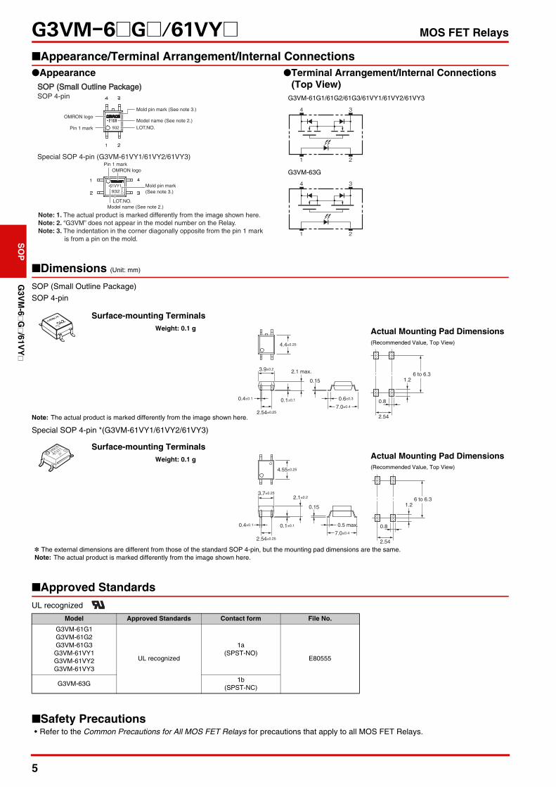
■Appearance/Terminal Arrangement/Internal Connections
■Dimensions (Unit: mm)
SOP (Small Outline Package)
SOP 4-pin
Special SOP 4-pin *(G3VM-61VY1/61VY2/61VY3)
■Approved StandardsUL recognized
■Safety Precautions• Refer to the Common Precautions for All MOS FET Relays for precautions that apply to all MOS FET Relays.
●Appearance ●Terminal Arrangement/Internal Connections(Top View)
Note: The actual product is marked differently from the image shown here.
Actual Mounting Pad Dimensions(Recommended Value, Top View)
Actual Mounting Pad Dimensions(Recommended Value, Top View)
* The external dimensions are different from those of the standard SOP 4-pin, but the mounting pad dimensions are the same.Note: The actual product is marked differently from the image shown here.
Model Approved Standards Contact form File No.
G3VM-61G1G3VM-61G2G3VM-61G3G3VM-61VY1G3VM-61VY2G3VM-61VY3
UL recognized
1a(SPST-NO)
E80555
G3VM-63G1b
(SPST-NC)
SOP 4-pinSOP (Small Outline Package)SOP (Small Outline Package)
OMRON logo
Pin 1 mark
Model name (See note 2.)
Mold pin mark (See note 3.)
LOT.NO.932
Note: 1. The actual product is marked differently from the image shown here.Note: 2. “G3VM” does not appear in the model number on the Relay.Note: 3. The indentation in the corner diagonally opposite from the pin 1 mark
is from a pin on the mold.
Mold pin mark (See note 3.)
Special SOP 4-pin (G3VM-61VY1/61VY2/61VY3)
OMRON logoPin 1 mark
Model name (See note 2.)
932-61VY1
LOT.NO.
G3VM-61G1/61G2/61G3/61VY1/61VY2/61VY3
G3VM-63G
Surface-mounting TerminalsWeight: 0.1 g
4.4±0.25
3.9±0.2
0.4±0.1
2.54±0.25
2.1 max.
0.1±0.1
7.0±0.4
0.6±0.3
0.156 to 6.3
1.2
0.8
2.54
Surface-mounting TerminalsWeight: 0.1 g
4.55±0.25
3.7±0.25
0.1±0.10.4±0.1
2.1±0.2
7.0±0.4
0.5 max.
0.15
2.54±0.25
6 to 6.31.2
0.8
2.54

6
G3VM-6@G@/61VY@ MOS FET RelaysS
OP
G3V
M-6
@G
@/61V
Y@
OMRON CorporationElectronic and Mechanical Components Company
Regional Contact
Cat. No. K282-E1-030318(0216)
Americas Europehttps://www.components.omron.com/ http://components.omron.eu/
Asia-Pacific China https://ecb.omron.com.sg/ https://www.ecb.omron.com.cn/
Korea Japanhttps://www.omron-ecb.co.kr/ https://www.omron.co.jp/ecb/
In the interest of product improvement, specifications are subject to change without notice.© OMRON Corporation 2018 All Rights Reserved.
Please check each region's Terms & Conditions by region website.