ganex iii-n newsletter - knowmade
TRANSCRIPT

Coordinated by CRHEA-CNRS research laboratory, this monthly newsletter is produced by Knowmade with collaboration from the managers of GANEX groups. The newsletter presents a selection of newest scientific publications, patent applications and press releases related to III-Nitride semiconductor materials (GaN, AlN, InN and alloys)
All issues on www.ganex.fr in Veille section. Free subscription http://www.knowmade.com/ganex
GANEX
Cluster of Excellence (Labex, 2012-2019) GANEX is a cluster gathering French research teams involved in GaN technology. The objective of GANEX is to strengthen the position of French academic players in terms of knowledge and visibility, and reinforce the French industrials in terms of know-how and market share. www.ganex.fr
KnowMade KnowMade is a Technology Intelligence and IP Strategy consulting company specialized in analysis of patents and scientific information. The company supports R&D organizations, industrial companies and investors in their business development by helping them to understand their competitive environment, follow technology trends, and find out opportunities and threats in terms of technology and patents. Knowmade operates in the following industrial sectors: Compound Semiconductors, Power Electronics, RF & Microwave Technologies, LED/OLED Lighting & Display, Photonics, Memories, MEMS & Sensors, Manufacturing & Advanced packaging, Batteries & Energy management, Biotechnology, Pharmaceuticals, Medical Devices, Medical Imaging, Agri-Food & Environment. Knowmade’s experts provide prior art search, patent landscape analysis, scientific literature analysis, patent valuation, IP due diligence and freedom-to-operate analysis. In parallel the company proposes litigation/licensing support, technology scouting and IP/technology watch service. Knowmade’s analysts combine their technical and patent expertise by using powerful analytics tools and proprietary methodologies to deliver relevant patent analyses and scientific reviews. www.knowmade.com
GANEX Newsletter No. 77 June 2019
III-N Technology

GaNEX | III-N Technology Newsletter No. 77 | 2
METHODOLOGY
Each month
150+ new scientific publications
200+ new patent applications
30+ new press releases
Sources 10+ scientific journal editors
Elsevier, IOP, IEEE, Wiley, Springer, APS, AIP, AVS, ECS, Nature, Science …
10+ specialist magazines Semiconductor Today, ElectoIQ, i-micronews,
Compound Semiconductor, Solid State Technology … 5+ open access database: FreeFulPDF, DOAJ …
Patent database: Questel-Orbit
Selection by III-N French
experts
GANEX monthly newsletter

GaNEX | III-N Technology Newsletter No. 77 | 3
TABLE OF CONTENTS (clickable links to chapters)
SCIENTIFIC PUBLICATIONS ............................................................................................................................. 4
GROUP 1 - LEDs and Lighting ................................................................................................................................. 4
GROUP 2 - Laser and Coherent Light ..................................................................................................................... 9
GROUP 3 - Power Electronics .............................................................................................................................. 12
GROUP 4 - Advanced Electronics and RF ............................................................................................................. 16
GROUP 5 – MEMS and Sensors............................................................................................................................ 22
GROUP 6 - Photovoltaics and Energy harvesting................................................................................................. 27
GROUP 7 - Materials, Technology and Fundamental .......................................................................................... 32
PRESS RELEASE ............................................................................................................................................ 46
PATENT APPLICATIONS ................................................................................................................................ 72

GaNEX | III-N Technology Newsletter No. 77 | 4
SCIENTIFIC PUBLICATIONS Selection of new scientific articles
GROUP 1 - LEDs and Lighting Group leader: Benjamin Damilano (CRHEA-CNRS)
Information selected by Mathieu Leroux (CRHEA-CNRS)
Highly polarized photoluminescence from c-plane
InGaN/GaN multiple quantum wells on stripe-
shaped cavity-engineered sapphire substrate Department of Materials Science and Engineering, Seoul
National University, Seoul, 08826, Korea
Department of Electronics Engineering, Catholic University
of Daegu, Gyeongbuk, 38430, Korea
Research Institute of Advanced Materials, Seoul National
University, Seoul, 08826, Korea
Inter-university Semiconductor Research Center, Seoul
National University, Seoul, 08826, Korea
Scientific Reports
https://doi.org/10.1038/s41598-019-44519-2
Highly polarized photoluminescence (PL) from c-
plane InGaN/GaN multiple quantum wells (MQWs)
grown on stripe-shaped cavity-engineered sapphire
substrate (SCES) was realized. The polarization ratio
was as high as 0.74 at room temperature. High-
resolution X-ray reciprocal space mapping
measurements revealed that the InGaN quantum
wells on GaN/SCES template were under
considerable anisotropic in-plane strain states of
−1.178% and −1.921% along the directions
perpendicular and parallel to the stripe-pattern,
respectively. The anisotropic strain states were
attributed to the anisotropic alignment of cavity-
incorporated sapphire nano-membranes, which
accommodated both anisotropic elastic relaxation in
the InGaN quantum well plane as well as the graded
elastic relaxation along the vertical direction in the
GaN template adjacent to the InGaN/GaN MQWs.
The partial strain relaxation in the InGaN wells also
contributed to reduction of quantum confined Stark
effect, resulting in four times higher PL intensity than
InGaN/GaN MQWs on planar sapphire substrate.
From theoretical calculations based on k∙p
perturbation theory, it was found that fundamental
origin of the polarized optical emission was strain-
induced modification of valence band structures of
the InGaN/GaN MQWs on the SCES. This study will
allow us to realize light emitting diodes with highly
polarized emission with conventional c-plane
sapphire substrates by strain-induced valence band
modification.
Correlation of Optical, Structural and Compositional
Properties with V-Pit Distribution in InGaN/GaN
Multi-Quantum Wells IHP- Leibniz-Institut für innovative Mikroelektronik, Im
Technologiepark 25, 15236 Frankfurt (Oder), Germany.
European Synchrotron Radiation Facility, BP 220, 38043
Grenoble Cedex, France.
Université Grenoble Alpes, CNRS, Grenoble INP, SIMAP,
38000 Grenoble, France.
OSRAM Opto Semiconductors GmbH, Leibnizstr. 4, 93055
Regensburg, Germany.
Department of Microsystems Engineering (IMTEK),
University of Freiburg, Georges-Köhler-Allee 103, 79110
Freiburg, Germany.
Institute of Physics, Technische Universität Chemnitz,
Reichenhainer Straße 70, 09126 Chemnitz, Germany.
Leibniz-Institut für Kristallzüchtung (IKZ), Max-Born Str.2,
12489 Berlin, Germany.
ACS Appl. Mater. Interfaces
https://doi.org/10.1021/acsami.9b04431
InGaN/GaN double heterostructures and multi-
quantum wells have been successfully developed
since more than 20 years for LED lightning
applications. Recent developments show that state-
of-the-art LEDs benefit from artificially generated V-
pit defects. However, the control of structural and
chemical properties plays a tremendous role. In this
paper we report on the lateral distribution of V-pit
defects and photoluminescence of InGaN/GaN multi
quantum wells grown on thick GaN on patterned
sapphire substrates. The synchrotron based scanning
x-ray diffraction microscopy technique K-Map was
employed to locally correlate these properties with
the local tilt, strain and composition of the
InGaN/GaN multi-quantum well. Compositional
fluctuation is the main factor for the variation of

GaNEX | III-N Technology Newsletter No. 77 | 5
photoluminescence intensity and broadening. In turn
V-pit defects, align along small-angle grain
boundaries, and their strain fields are identified as
reason for promoting the InGaN segregation process
on a microscale.
Effect of electron blocking layer on the efficiency of
AlGaN mid-ultraviolet light emitting diodes Department of Electrical Engineering and Computer
Science, University of Michigan, 1301 Beal Avenue, Ann
Arbor, Michigan, MI 48109, USA
Department of Electrical and Computer Engineering,
McGill University, 3480 University Street, Montreal,
Quebec H3A 0E9, Canada
Optics Express
https://doi.org/10.1364/OE.27.00A738
The performance of AlGaN-based mid and deep
ultraviolet light emitting diodes (LEDs) is severely
limited by electron overflow and by the poor hole
injection into the device active region. We have
studied the effect of various electron blocking layers
on the performance of AlGaN LEDs operating at ~280
nm. It is observed that, compared to conventional p-
type electron blocking layer, the incorporation of an
n-type AlN/AlGaN superlattice electron blocking layer
before the active region can significantly improve the
device performance by reducing electron overflow
without compromising hole injection. Direct on-wafer
measurement showed an external quantum
efficiency ~4.4% and wall-plug efficiency ~2.8% by
optimizing the design of n-type AlN/AlGaN
superlattice electron blocking layer, which is nearly a
factor of five to ten times better than identical
devices but with the incorporation of a conventional
p-type electron blocking layer.
Influence of LO and LA phonon processes on
thermal-nonequilibrium excitation and deexcitation
dynamics of excitons in GaN, AlN, and ZnO Department of Electrical and Electronic Engineering, Chiba
University, 1-33 Yayoicho, Inage-ku, Chiba 263-8522, Japan
Journal of Applied Physics
https://doi.org/10.1063/1.5092620
The 1S-exciton density NX(1) in GaN, AlN, and ZnO is
calculated for thermal-nonequilibrium states where
the temperatures of an electron–hole system and
phonons are different in the range of 10–400 K. The
ratio of NX(1) in AlN to that in ZnO reaches 21 despite
the similar exciton-binding energies of AlN and ZnO,
which is due to the higher rate of excitation by LO-
phonon absorption in ZnO. This result reveals that
thermal-nonequilibrium states significantly affect the
validity of evaluation methods for physical
parameters such as internal quantum efficiency of
radiation. The ratio of NX(1) in AlN to that in ZnO is
enhanced from 2.2 to 18 by the occupation of states
of the principal quantum number n from 2 to 5. This
result demonstrates the importance of the discussion
on the n≥3 states which have not been taken into
account in other analyses. The main reason for the
decrease in NX(1) is found to be the increase in the
temperature of LO phonons rather than LA phonons,
which indicates the importance of LO-phonon control
in light-emitting devices. The results for general
thermal-nonequilibrium states are nontrivial because
the mechanisms of the population balance are
complicated owing to the several-n occupation and
the transition rates determined by various factors.
Our analyses and discussions quantitatively unveil the
LO- and LA-phonon effects on the thermal-
nonequilibrium excitation and deexcitation dynamics
of excitons and provide the basis for design of highly
efficient light-emitting devices particularly in the
ultraviolet region.
Modification of strain and optical polarization
property in AlGaN multiple quantum wells by
introducing ultrathin AlN layer Engineering Research Center of Micro-nano Optoelectronic
Materials and Devices, Ministry of Education; Fujian Key
Laboratory of Semiconductor Materials and Applications,
CI Center for OSED, Jiujiang Res Inst and Department of
Physics, Xiamen University, Xiamen 361005, China
AIP Advances
https://doi.org/10.1063/1.5091027
The effects of ultrathin AlN insertion layers on the
strain status, as well as optical properties of AlGaN
multiple quantum wells (MQWs), were studied. A
large stress variation of about -1.46 GPa can be
achieved by introducing two ultrathin AlN layers at
each interface between the quantum well and the
barrier, thereby resulting in the fact that the degree

GaNEX | III-N Technology Newsletter No. 77 | 6
of polarization is increased from 17.8% to 22.3% in
traditional MQWs. In addition, the quantum well
emission are found to become symmetric and
narrower due to the suppression of compositional
fluctuation. These results provide a simple technique
to modify the strain field of MQWs so as to improve
transverse-electric polarized emission for deep
ultraviolet light emitting diodes.
Polarization control in nitride quantum well light
emitters enabled by bottom tunnel-junctions Department of Electrical and Computer Engineering,
Cornell University, Ithaca, New York 14853, USA
Institute of High Pressure Physics, Polish Academy of
Sciences, Sokołowska 29/37, PL-01-142 Warsaw, Poland
Department of Materials Science and Engineering, Cornell
University, Ithaca, New York 14853, USA
Kavli Institute for Nanoscale Science, Cornell University,
Ithaca, New York 14853, USA
Journal of Applied Physics
https://doi.org/10.1063/1.5088041
The frozen internal polarization-induced electric
fields due to broken inversion symmetry in all
conventional blue and green nitride semiconductor
light-emitting semiconductor quantum well
heterostructures point in a direction opposite to
what is desired for efficient flow of electrons and
holes. This state of affairs has persisted because of
the desire to have p-type hole injectors on top of the
quantum well active region. Because of the internal
polarization fields in nitride heterostructures, there
exist four permutations of doping and polarization for
the realization of such light emitters. Which
permutation is the most desirable for efficient light
emission? In this work, we answer this question by
demonstrating a fundamentally new approach
toward efficient light emission with “bottom-tunnel
junctions.” The bottom-tunnel junction design aligns
the polarization fields in the desired direction in the
quantum well while simultaneously eliminating the
need for p-type contacts and allowing efficient
current spreading. By preventing electron overshoot
past quantum wells, it disables carrier recombination
in undesired regions of the quantized
heterostructures and opens up the possibility for new
geometries of integrating and stacking multiple light
emitters.
Enhanced Performance of InGaN‐Based Blue LEDs
Using an AlGaN/InGaN Super‐Lattice Last Quantum
Barrier Wuhan National Laboratory for Optoelectronics, Huazhong
University of Science and Technology, Wuhan 430074,
China
physica status solidi a
https://doi.org/10.1002/pssa.201800913
In this work, a novel structure of InGaN‐based blue
light‐emitting diodes (LEDs) using a super‐lattice
structure as the last quantum barrier (QB) in the
active region is proposed to improve the blue LEDs
performance. The optical power and external
quantum efficiency (EQE) are investigated by both
simulation and experiment. The proposed
super‐lattice last QB can significantly enhance the
effective barrier of electrons from 463 to 576 meV in
the conduction band and thus block the leakage of
electrons. It is found that such structure can also
facilitate the hole injection due to the reduced
effective barrier height from 293 to 261 meV in the
valance band. Eventually, the increase of the carrier
concentration in the active region further improves
the internal quantum efficiency (IQE) of the device.
The experimental results indicate that the output
power of the proposed LED is increased by 16.9%
compared with the conventional LED, with lower
efficiency droop (less than 20.65%). The proposed
structure can be an alternative in pursuing high
efficiency blue LEDs in the future.
Growth and characterization of InxGa1−xN
(0 < x < 0.16) templates for controlled emissions
from MQW Department of Electrical and Computer Engineering, North
Carolina State University, Raleigh, NC 27695, USA
Department of Materials Science and Engineering, North
Carolina State University, Raleigh, NC 27695, USA
Journal of Crystal Growth
https://doi.org/10.1016/j.jcrysgro.2019.05.019
InxGa1−xN (0 < x < 0.16) templates were grown by
Metal Organic Chemical Vapor Deposition (MOCVD)
using the semibulk (SB) growth approach. We have
studied the impact of different SB design parameters
such as the number of (InGaN/GaN) periods, InGaN

GaNEX | III-N Technology Newsletter No. 77 | 7
layer thickness (T), and the GaN substrate quality on
the SB-template properties, and its degree of
relaxation. SIMS characterization measured the
variation of indium content (x) in the template, while
photoluminescence reflected the indium content at
the topmost layers of the SB template. X-ray
diffraction techniques measured the average lattice
parameters and degree of strain relaxation through
the entire InxGa1−xN SB-templates. The SB approach
results in superior material quality relative to the bulk
grown InGaN, mainly due to its ability to avoid the
inclusion of indium-rich clusters and V-pits in the SB
templates. The SB approach slows down the
relaxation processes and templates as thick as
750 nm are not fully relaxed. We are reporting on
methods to enhance the relaxation processes in
InxGa1−xN SB-templates. Finally, when InxGa1−xN
templates with 0 ≤ x ≤ 0.16 are used as substrates for
InGaN/GaN multiple quantum wells, the emission
wavelength is shifted from blue to green by changing
the indium content in the InxGa1−xN SB-templates.
To the best of our knowledge, the current results
present the highest indium content reported in
InxGa1−xN SB-templates.
Recent progress of tunnel junction-based ultra-
violet light emitting diodes Department of Electrical and Computer Engineering, The
Ohio State University, Columbus, Ohio, 43210, United
States of America
Department of Materials Science and Engineering, The
Ohio State University, Columbus, Ohio, 43210, United
States of America
Japanese Journal of Applied Physics
https://doi.org/10.7567/1347-4065/ab1254
AlGaN-based UV LEDs are promising for a wide range
of industrial, household and healthcare applications.
However, widespread adoption of UV LEDs is limited
by the poor device efficiency. This has been
attributed to the strong internal light absorption and
poor electrical injection efficiency associated with the
conventional UV LED structures, which typically use
an absorbing p-GaN layer for p-type contact. Recent
development of ultra-wide bandgap AlGaN tunnel
junctions enabled a novel UV LED design with the
absence of the absorbing p-GaN contact layer. In this
work, we review the recent progress of AlGaN tunnel
junctions and the development of tunnel junction-
based UV LEDs, and discuss the challenges and future
perspectives for the realization of high power, high
efficiency UV LEDs.
The polarization field in Al-rich AlGaN multiple
quantum wells Department of Materials Science and Engineering, North
Carolina State University, Raleigh, NC 27695, United States
of America
Adroit Materials, 2054 Kildaire Farm Rd, Suite 205, Cary,
NC 27518, United States of America
Japanese Journal of Applied Physics
https://doi.org/10.7567/1347-4065/ab07a9
This paper investigates the quantum confined Stark
effect in AlGaN multiple quantum well structures
with a high Al content grown on single-crystalline AlN
substrates. The quantitative relationship between the
quantum well structure parameters, photogenerated
carrier density, built-in electric field and ground-level
emission is discussed. It is found that the electric field
strength increases from 0.5 MV cm−1 to almost 3 MV
cm−1 when the Al content in the quantum well
barriers is increased from 65% to 100%, which is
consistent with the theory of spontaneous and
piezoelectric polarization in III-nitrides. In addition,
the built-in electric field increases significantly with
increasing barrier thickness. Based on these results,
the electric field in an Al0.55Ga0.45N single quantum
well with AlN cladding is predicted to be around 5 MV
cm−1.
Study of AlN based materials grown on nano-
patterned sapphire substrates for deep ultraviolet
LED applications Advanced Micro-Fabrication Equipment Inc., 188 Taihua
Road, Shanghai, People's Republic of China
Japanese Journal of Applied Physics
https://doi.org/10.7567/1347-4065/ab09de
High quality and crack-free AlN films were obtained
by using nano-patterned sapphire substrates (NPSS)
grown at AMEC Prismo HiT3TM MOCVD platform. It
is believed that the introduced epitaxial lateral
overgrowth can annihilate most of dislocations and
the grain boundary induced tensile stress can be

GaNEX | III-N Technology Newsletter No. 77 | 8
significantly suppressed by NPSS. For a 5 μm thick AlN
film, FWHMs of 173 arcsec and 335 arcsec were
observed from AlN (002) and (102) X-ray rocking
curves, respectively, indicating the high crystalline
quality. The surface of AlN films grown on NPSS
shows a typical step-bunching morphology with
atomic steps on the bunched terrace. In addition, we
also obtained excellent thickness uniformity for AlN
films grown on NPSS with within-wafer and wafer-to-
wafer thickness uniformity of 0.69% and 0.92%,
respectively.
Enhanced Wall-Plug Efficiency in AlGaN-Based Deep-
Ultraviolet LED via a Novel Honeycomb Hole-Shaped
Structure Wuhan National Laboratory for Optoelectronics, Huazhong
University of Science and Technology, Wuhan 430074,
China
State Key Laboratory of Infrared Physics, Shanghai Institute
of Technical Physics, Chinese Academy of Sciences,
Shanghai 200083, China.
IEEE Transactions on Electron Devices
https://doi.org/10.1109/TED.2019.2913962
The novel honeycomb hole-shaped electrode (HHSE)
structure was proposed for 280-nm AlGaN-based flip-
chip deep-ultraviolet light emitting diode (DUV-LED),
which was demonstrated to be beneficial to the
current spreading, optical emission, and heat
dispersion. By means of the finite element method,
we investigated the current density distribution at an
injection current density of 67.5 A/cm² and found
that the effective current spreading area was
approximately improved by 35.3% for the light
emitting diode (LED) with a novel electrode
compared with the LED with the conventional finger-
shape electrode. As a result, the wall-plug efficiency
(WPE) of the LED with a novel electrode was
increased by 28% at an injection current of 280 mA.
Meanwhile, the symmetrical distribution of optical
emission and temperature was realized. This paper
paves the way to solve the current crowding effect
due to the poor conductivity of the n-AlGaN layers
with high Al fraction and significantly develop high
efficiency in the AlGaN-based DUV-LED.
Effects of Meshed p-type Contact Structure on the
Light Extraction Effect for Deep Ultraviolet Flip-Chip
Light-Emitting Diodes Key Laboratory of Electronic Materials and Devices of
Tianjin, School of Electronics and Information Engineering,
Hebei University of Technology, Tianjin, People’s Republic
of China
Nanoscale Research Letters
https://doi.org/10.1186/s11671-019-2984-0
In this work, flip-chip AlGaN-based deep ultraviolet
light-emitting diodes (DUV LEDs) with various
meshed contact structures are systematically
investigated via three-dimensional finite-difference
time-domain (3D FDTD) method. It is observed that
both transverse electric (TE)- and transverse
magnetic (TM)-polarized light extraction efficiencies
(LEEs) are sensitive to the spacing and inclined angle
for the meshed structure. We also find that the LEE
will not be increased when a large filling factor is
adopted for the meshed structures, which is because
of the competition among the p-GaN layer
absorption, the Al metal plasmon resonant
absorption, and the scattering effect by meshed
structures. The very strong scattering effect occurring
in the hybrid p-GaN nanorod/p-AlGaN truncated
nanocone contacts can enormously enhance the LEE
for both TE- and TM-polarized light, e.g., when the
inclined angle is 30°, the LEE for the TE- and TM-
polarized light can be increased by ~ 5 times and ~ 24
times at the emission wavelength of 280 nm,
respectively.

GaNEX | III-N Technology Newsletter No. 77 | 9
GROUP 2 - Laser and Coherent Light Group leader: Bruno Gayral (CEA)
Information selected by Knowmade
Analysis of optical injection on red and blue laser
diodes for high bit-rate visible light communication Optoelectronics Research Laboratory, Electrical
Engineering Department, King Fahd University of
Petroleum & Minerals, Dhahran 31261, Saudi Arabia
Photonics Laboratory, Computer, Electrical and
Mathematical Sciences and Engineering (CEMSE) division,
King Abdullah University of Science & Technology (KAUST),
Thuwal 23955-6900, Saudi Arabia
Optics Communications
https://doi.org/10.1016/j.optcom.2019.05.034
In this work, self-injection and external-injection in
450 nm InGaN/GaN blue and 650 nm InGaP/AlGaInP
red diode lasers are investigated. A distinct locking
characteristic is observed in the self-injection case
with small 19 cm cavity length, demonstrating
enhanced 2.34 and 2.07 GHz 3-dB bandwidths,
corresponding to a factor of 1.4 and 1.1
improvement, and reduced 60 and 80 pm spectral
linewidths, for the blue and the red lasers,
respectively. Moreover, this short external cavity self-
injection locked system exhibited superior
performance by a factor of 1.1–1.3 compared to the
long cavity (26 cm) configuration. Conversely, the
external optical injection exhibited weak locking
signature with improved linewidths by a factor of
1.6–2.8 and reaching as small as 70 and 87 pm for the
blue laser, respectively, while almost doubling in the
peak powers. Later, on–off keying modulation
technique based data transmission rates of up to 3.5
and 4.5 Gb/s are demonstrated on free-running blue
and red laser diodes, respectively, employing an in-
house laser diode mount based system. Moreover,
owing to the bandwidth limitation of the optically
injected systems, successful transmission of up to 2
Gb/s is demonstrated with better performance
compared to the respective free-running cases, in
particular, the external-optically injected system
demonstrated more than double improvement in the
bit-error-rate.
Single and Multiple Longitudinal Wavelength
Generation in Green Diode Laser Electrical and Computer Engineering, McGill University,
5620 Montreal, Quebec Canada H3A 0G4
CEMSE, King Abdullah University of Science and
Technology, Thuwal, Makkah Saudi Arabia 23955-6900
Electrical Engineering, King Abdullah University of Science
and Technology, 127355 Thuwal, Mecca Saudi Arabia
23955-6900
Electrical Engineering Department, King Fahd University of
Petroleum and minerals, Dhahran, Eastern Province Saudi
Arabia 31261
IEEE Journal of Selected Topics in Quantum Electronics
https://doi.org/10.1109/JSTQE.2019.2916870
Single and multiple wavelength laser systems are
presented that employ self-injection locked
InGaN/GaN green laser diode in an external cavity
configuration with a partially reflective mirror. A
stable and simultaneous locking of up to 4
longitudinal Fabry-Perot modes of the system cavity
is demonstrated with appreciable signal-to-noise-
ratio (SNR) of ~13 dB and average mode linewidth of
~150 pm. The multi-wavelength spectrum exhibited a
flat-top emission with nearly equal power
distribution among the modes and an analogous
mode spacing of ~0.5 nm. This first demonstration of
multi-wavelength generation source is highly
attractive in multitude of cross-disciplinary field
applications besides asserting the prospects of
narrow wavelength spaced multiplexed visible light
communication. Moreover, an extended two-stage
self-injection locked near single wavelength visible
laser system is also presented. An ultra-narrow
linewidth of ~34 pm is realized at 525.05 nm locked
wavelength from this novel system, with ~20 dB side-
mode-suppression-ratio (SMSR); thus signifying a
paradigm shift towards semiconductor lasers for near
single lasing wavelength generation, which is
presently dominated by other kinds of laser
technologies.

GaNEX | III-N Technology Newsletter No. 77 | 10
Tunable GaN photonic crystal and microdisk on
PDMS flexible film Department of Electrical and Electronic Engineering, The
University of Hong Kong, Pokfulam Road, Hong Kong
ACS Appl. Electron. Mater.
https://doi.org/10.1021/acsaelm.9b00114
Flexible micro-/nano-scale photonics has shown great
promise in a wide range of applications, especially
those that cannot be addressed by traditional
photonics based on rigid materials and structures.
Flexible photonics are typically implemented by
transferring compact optical devices made in high-
quality crystalline semiconductors onto plastic
substrates. However, success in developing flexible
optical devices based on GaN micro-/nano-structures
has been extremely limited. In this work, we target to
overcome this bottleneck by forming GaN photonic
crystals and microdisks on flexible PDMS films using a
combination of nano-/micro-sphere lithography and
laser lift-off techniques. The GaN-PDMS
configurations not only endow the devices with
mechanical flexibility but also enable optical tuning of
the photonic bandgaps from stretchable photonic
crystals and whispering-gallery-mode laser emission
from bendable microdisks over a remarkably large
range. Their optical properties of the devices are
extensively studied through a range of spectroscopy
techniques and simulations. The present
demonstrations verify the feasibility of the proposed
GaN-PDMS platform for forming compact flexible
devices, which could pave the way towards emerging
applications of flexible photonics technology.
Light confinement and high current density in UVB
laser diode structure using Al composition-graded p-
AlGaN cladding layer Asahi-Kasei Corporation, Fuji, Shizuoka 416-8501, Japan
Faculty of Science and Technology, Meijo University,
Nagoya 468-8502, Japan
Akasaki Research Center, Nagoya University, Nagoya 464-
8603, Japan
Applied Physics Letters
https://doi.org/10.1063/1.5095149
In this study, we investigated laser characteristics via
photoexcitation and electro-optical characteristics via
current injection in ultraviolet (UV)-B laser diodes. To
achieve light confinement and high current injection,
an Al composition-graded 260-nm thick p-type
Al0.9→0.45Ga0.1→0.55N cladding layer was
designed, which exhibited a calculated light
confinement factor of 3.5%. Laser oscillation with a
threshold at 275 kW/cm2 at 297 nm was obtained via
the photoexcited measurement. A prototype device
for current injection was designed using the p-
Al0.9→0.45Ga0.1→0.55N cladding layer and an
additional Al composition-graded 75-nm thick p-type
Al0.45→0Ga0.55→1N layer for the p-type contact
layer. The maximum current density in the device
reached 41.2 kA/cm2, which is the highest ever
reported value among light-emitting devices
operating in the UVB and ultraviolet-C regions. The
peak wavelength of the emission spectrum obtained
from the mirror facet was 300 nm, corresponding to
the double quantum wells, without any significant
droop. Further, a subpeak emission at 275 nm was
observed, which is likely caused by the waveguide
layer by electron overflow.
GaN-based ultraviolet microdisk laser diode grown
on Si Key Laboratory of Nano-Devices and Applications, Suzhou
Institute of Nano-Tech and Nano-Bionics, Chinese
Academy of Sciences, Suzhou 215123, China
University of Science and Technology Beijing, Beijing
100083, China
Suzhou Institute of Nano-Tech and Nano-Bionics, Chinese
Academy of Sciences, Nanchang 330200, China
School of Nano Technology and Nano Bionics, University of
Science and Technology of China, Hefei 230026, China
Photonics Research
https://doi.org/10.1364/PRJ.7.000B32
This work reports a demonstration of electrically
injected GaN-based near-ultraviolet microdisk laser
diodes with a lasing wavelength of 386.3 nm at room
temperature. The crack-free laser structure was
epitaxially grown on Si substrates using an Al-
composed down-graded AlN/AlGaN multilayer buffer
to mitigate the mismatches in the lattice constant
and coefficient of thermal expansion, and processed
into “sandwich-like” microdisk structures with a
radius of 12 μm. Air-bridge electrodes were
successfully fabricated to enable the device electrical

GaNEX | III-N Technology Newsletter No. 77 | 11
characterization. The electrically pumped lasing of
the as-fabricated microdisk laser diodes was
evidenced by the rapid narrowing down of
electroluminescence spectra and dramatic increase in
the light output power, as the current exceeded the
threshold of 248 mA.
Impact of quantum dots on III-nitride lasers: a
theoretical calculation of threshold current densities Institute for Nano Quantum Information Electronics, The
University of Tokyo, 4-6-1, Komaba, Meguro-ku, Tokyo,
153-8505, Japan
Japanese Journal of Applied Physics
https://doi.org/10.7567/1347-4065/ab1068
We present a theoretical study on the gain and
threshold current density of III-nitride quantum dot
(QD) and quantum well (QW) lasers with a
comprehensive theory model. It is found that at
transparency condition the injection current density
of QD lasers is about 120 times lower than QW lasers
in III-nitrides, while in III-arsenide it is about 15 times.
It means that using QDs in III-nitride lasers could be 8
times more efficient than in III-arsenide. This
significant improvement in III-nitrides is due to their
large effective-masses and the large asymmetry of
effective-masses between valence bands and
conduction bands. Our results reveal the advantages
of using QD for low threshold laser applications in III-
nitrides.
Large-area, liftoff nanoporous GaN distributed Bragg
reflectors: Fabrication and application School of Microelectronics, Shandong University, Jinan
250100, China
School of Physics, Shandong University, Jinan 250100,
China
School of Science, Xi'an Polytechnic University, Xi'an
710048, China
Applied Surface Science
https://doi.org/10.1016/j.apsusc.2019.05.128
A facile one-step electrochemical etching based on
NaNO3 solution was developed for use in the
chemical lift-off nanoporous- (NP-) GaN distributed
Bragg reflectors (DBRs) over a macroscopic area
(>1 cm2). The reflectivity of the lift-off DBR mirror is
~85%, which is far lower than that (~97%) of the NP-
GaN DBR on the sapphire substrate. The decrease
should be attributed to light scattering due to higher
roughness in the lift-off mirror. To study its possible
applications, tris(8-hydroxyquinoline) aluminum (III)
(Alq3) thin film was grown on transferred NP-GaN
DBR mirror onto silicon substrate via a thermal
evaporation deposition. Compared to the reference
Alq3 thin film, the photoluminescence of the Alq3
thin film on the transferred mirror presents
significant enhancement and slight blue-shift, which
should be attributable to reflectivity enhancement by
the DBR and inner channel surface in the DBR mirror,
respectively.
Omnidirectional whispering-gallery-mode lasing in
GaN microdisk obtained by selective area growth on
sapphire substrate School of Physical Science and Technology, ShanghaiTech
University, Pudong, Shanghai, 201210, China
Ningbo Institute of Materials Technology and Engineering,
Chinese Academy of Sciences, Ningbo, 315201, Zhejiang,
China
University of Chinese Academy of Sciences, Beijing,
100049, China
School of Materials Science and Engineering, Shanghai
University, Shanghai, 200444, China
Department of Electrical and Electronic Engineering,
Faculty of Science and Engineering, University of
Nottingham Ningbo China, Ningbo 315100, China
Advanced Micro-Fabrication Equipment Inc. Shanghai,
201201, China
Optics Express
https://doi.org/10.1364/OE.27.016195
The optical properties of hexagonal GaN microdisk
arrays grown on sapphire substrates by selective area
growth (SAG) technique were investigated both
experimentally and theoretically. Whispering-gallery-
mode (WGM) lasing is observed from various
directions of the GaN pyramids collected at room
temperature, with the dominant lasing mode being
Transverse-Electric (TE) polarized. A relaxation of
compressive strain in the lateral overgrown region of
the GaN microdisk is illustrated by
photoluminescence (PL) mapping and Raman
spectroscopy. A strong correlation between the
crystalline quality and lasing behavior of the GaN
microdisks was also demonstrated.

GaNEX | III-N Technology Newsletter No. 77 | 12
GROUP 3 - Power Electronics Group leader: Frédéric Morancho (LAAS-CNRS)
Information selected by Frédéric Morancho (LAAS-CNRS) and Yvon Cordier (CRHEA-CNRS)
Characterization and optimization of MIS-HEMTs
device of high~k dielectric material on quaternary
barrier of Al0.42ln0.03Ga0.55N/UID-AIN/GaN/GaN
heterostructure for high power switching
application Department of Physics and Nanotechnology, Faculty of
Engineering and Technology, SRM Institute of Science and
Technology, Kattankulathur 603203, Chennai, India
Applied Surface Science
https://doi.org/10.1016/j.apsusc.2019.05.170
In this study, the structure of efficient recessed gate
Metal Insulator Semiconductor High Electron Mobility
Transistor with Quaternary Barrier materials of
Al0.42ln0.03Ga0.55N was simulated and presented.
The device with heterostructure of
Al0.42ln0.03Ga0.55N/UID-AIN/GaN/GaN and
thickness of 5 nm/10 nm/40 nm/10 μm on SiC
substrate shows normally-OFF characteristics. The
effect of high~k dielectrics of HfAlxOx and the
quaternary barrier on the electrical performance of
the device was analyzed and compared with the
conventional AlGaN/GaN heterostructure. We found
that the charge optimization concept of the
polarization induced charges of the device 2DEG in
the channel was due to the combination of the
Quaternary Barrier of Al0.42ln0.03Ga0.55N and the
high~k dielectrics of HfAlxOx. Furthermore, the two
field plates used which are having a length of plate at
the drain (LGFP) of 1.8 μm and field plate at the
source (LGPS) 0.5 μm effectively spread the electric
field lines with the drain and showed a significant
improvement in the electrical properties of the
device and achieved a maximum drain current of
710 mA/mmV, low transconductance (gm) of 0.158
Smm−1 and high breakdown voltage of 570 V. In
comparison to the conventional AlGaN/GaN MIS-
HEMTs of similar design, the result of this Quaternary
Barrier Metal Insulator Semiconductor High Electron
Mobility Transistor (QB-MIS-HEMTs) exhibited a
better interface property, remarkable suppression of
leakage current, and excellent breakdown voltage
which are important for power switching
applications.
High-voltage vertical GaN-on-GaN Schottky barrier
diode using fluorine ion implantation treatment Suzhou Institute of Nano-tech and Nano-bionics, Chinese
Academy of Sciences, Suzhou 215123, PR China
School of Physical Science and Technology, ShanghaiTech
University, Shanghai 201210, PR China
University of Chinese Academy of Sciences, Beijing 100049,
PR China
Shanghai Institute of Ceramics, Chinese Academy of
Sciences, Shanghai 200050, PR China
Suzhou Nanowin Science and Technology Co., Ltd., Suzhou
215123, PR China
School of Nano Technology and Nano Bionics, University of
Science and Technology of China, Hefei 230026, PR China
AIP Advances
https://doi.org/10.1063/1.5100251
This paper reports on a high-voltage vertical GaN
Schottky barrier diode (SBD) using fluorine (F) ion
implantation treatment. Compared with the GaN SBD
without F implantation, this SBD effectively enhanced
the breakdown voltage from 155V to 775V and
significantly reduced the reverse leakage current by
105 times. These results indicate that the F-
implanted SBD showed improved reverse capability.
In addition, a high Ion/Ioff ratio of 108 and high
Schottky barrier height of 0.92 eV were also achieved
for this diode with F implantation. The influence of F
ion implantation in this SBD was also discussed in
detail. It was found that F ion implantation to GaN
could not only create a high-resistant region as
effective edge termination but be employed for
adjusting the carrier density of the surface of GaN,
which were both helpful to achieve high breakdown
voltage and suppress reverse leakage current. This
work shows the potential for fabricating high-voltage
and low-leakage SBDs using F ion implantation
treatment.

GaNEX | III-N Technology Newsletter No. 77 | 13
Characterization and modeling of 2DEG mobility in
AlGaN/AlN/GaN MIS-HEMT Univ. Grenoble Alpes, CEA-LETI, MINATEC, Grenoble,
France
Univ. Grenoble Alpes, IMEP-LAHC, MINATEC/INPG,
Grenoble, France
Microelectronic Engineering
https://doi.org/10.1016/j.mee.2019.05.003
We present a detailed study of the process influence
on two-dimensional electron gas (2DEG) transport
properties in Al0.25Ga0.75N/AlN/GaN
heterostructure. Hall effect measurements are used
to analyze the conduction in normally on devices
demonstrating the formation of a second channel at
the Al2O3/AlGaN interface for high biases. Electrical
characterization is performed on a large set of
devices for temperatures ranging from 25 °C to
250 °C, and 2DEG mobility is extracted using split C-V
measurement technique. Various technological splits
were experimentally tested and the corresponding
mobility characteristics were modeled using the
Kubo-Greenwood formula in order to determine the
dominant scattering phenomenon limiting the 2DEG
mobility.
A Rigorous Investigation of Electrostatic and
Transport Phenomena of GaN Double-Channel
HEMT Department of Electrical and Electronic Engineering,
Bangladesh University of Engineering and Technology,
Dhaka 1205, Bangladesh.
IEEE Transactions on Electron Devices
https://doi.org/10.1109/TED.2019.2915837
This paper presents a comprehensive investigation of
electrostatics and transport characterization of GaN
double-channel (DC) MOS-HEMT. Upon derivation of
a polynomial analytical expression establishing a
relationship between the Fermi level and the 2-D
electron gas density (2DEG), a relationship between
the sheet carrier density and applied gate voltage has
been obtained. To confirm the validity of the model
in both subthreshold and strong inversion regions,
the charge density profile and capacitance-voltage
profile have been attained from self-consistent
simulation incorporating the quantum mechanical
effect. The impact of GaN channel thickness on the
conduction band profile as well as charge density
profile has also been investigated. A 2-D analytical
model for current-voltage characteristics of GaN-DC-
MOS-HEMT has been developed for the first time.
Assuming velocity saturation of electrons in 2DEG,
the effects of spontaneous and piezoelectric
polarization at the heterointerface, field dependent
mobility, and the parasitic source and drain
resistance have been taken into account in evolution
of this model. The on-resistance extracted from the
analytical model was found to be 7.1 Ω·mm, which is
in close proximity with experimental results. A steep
subthreshold swing of 79 mV/dec was determined
from the current-voltage characteristics with an on-
off drain current ratio of the order of 10⁹, which
holds the promising application for enhancement
mode operation with minimal leakage current. For
corroboration, the derived results were compared
with experimental data acquired from the literature,
thereby enhancing the reliability of this model.
Effect of thermal cleaning prior to p-GaN gate
regrowth for normally-off high electron mobility
transistors School of Nano Technology and Nano Bionics, University of
Science and Technology of China, Hefei 230026, China
Key Laboratory of Nanodevices and Applications, Suzhou
Institute of NanoTech and NanoBionics, Chinese Academy
of Science, Suzhou 215123, China
ACS Appl. Mater. Interfaces
https://doi.org/10.1021/acsami.9b03130
This work studied the effect of thermal cleaning in
metal-organic chemical vapor deposition (MOCVD)
prior to p-GaN gate regrowth for normally-off high-
electron-mobility transistors (HEMTs). X-ray
photoelectron spectroscopy, capacitance-voltage
measurement and atomic force microscopy were
employed to identify the effects of thermal cleaning
before p-GaN regrowth. It was found that the
residual damages were hardly repaired at a relatively
low thermal cleaning temperature, while GaN
decomposition would occur at an excessively high
temperature. Thermal cleaning at 850 oC for 2 min in
MOCVD can effectively remove the surface
contamination and alleviate the etch damage without
causing any significant deterioration of the AlGaN
GaNEX | III-N Technology Newsletter No. 77 | 14
barrier. And the Dit in p-GaN gate was reduced from
1012~1013 to 1011~1012 eV-1·cm-2, resulting in a
low gate reverse leakage of 0.1 nA/mm @ VDS-
OFF=180 V, a high Ion/Ioff ratio of 4×10¹⁰, and a
relatively high threshold voltage of +1.7 V @ ID=10
μA/mm.
Formation of conductive AlN buffer layer using
spontaneous via-holes and realization of vertical
AlGaN Schottky diode on a Si substrate Research Organization of Science and Technology,
Ritsumeikan University, 1-1-1, Noji-higashi, Kusatsu, Shiga
525-8577, Japan
Journal of Applied Physics
https://doi.org/10.1063/1.5058110
A conductive AlN epitaxial layer is successfully
realized by spontaneously forming via-holes filled
with n-AlGaN inside an AlN buffer layer on a Si
substrate. The via-holes are found to originate from
the formation of an Al–Si alloy, produced from a
small amount of Al supplied to the Si substrate at the
initial stage of the crystal growth of the n-AlN buffer
layer using metal organic chemical vapor deposition
and successive selective growth of n-AlN on the Si
surface. The via-holes are filled with conductive n-
AlGaN by successive epitaxial growth of n-AlGaN,
making the insulating n-AlN buffer layer conductive.
The vertical conductivity through this n-AlN buffer
layer is enhanced more than 540 times compared
with an n-AlN buffer layer without via-holes. Using
this conductive n-AlN buffer layer on the Si substrate,
we successfully fabricated a vertical n-AlGaN Schottky
diode on the Si substrate for the first time.
A large-signal Pspice modeling of GaN-based MIS-
HEMTs School of Advanced Materials and Nanotechnology, Xidian
University, Xi'an 710126, China
Key Laboratory of Microelectronics Devices and Integrated
Technology, Institute of Microelectronics of Chinese
Academy of Sciences, Beijing 100029, China
Superlattices and Microstructures
https://doi.org/10.1016/j.spmi.2019.05.023
In this work we present a physics-based semi-
empirical large-signal model for GaN MIS-HEMTs,
which introduces the non-segmented, smooth
continuous equations to describe the static and
dynamic characteristics of GaN MIS-HEMTs in
different working regions. The unique physical effect
of threshold voltage drift was considered for MIS-
HEMTs in the current model, in addition to effects of
the channel length modulation and the temperature
drift. In addition, a current-controlled current source
was used in the dynamic model to characterize the
nonlinear capacitance including the gate-drain
capacitance CGD, gate-source capacitance CGS and
drain-source capacitance CDS at different operating
voltages. The model is in excellent agreement with
the experimental data for both drain current and
capacitances over a typical range of applied voltages
and temperatures.
Comparative Study Between Partially and Fully
Recessed‐Gate Enhancement‐Mode AlGaN/GaN MIS
HEMT on the Breakdown Mechanism State Key Discipline Laboratory of Wide Band-gap
Semiconductor Technology, School of Microelectronics,
Xidian University, Shaanxi 710071, People’s Republic of
China
School of Physics and Optoelectronic Engineering, Xidian
University, Shaanxi 710071, People’s Republic of China
physica status solidi a
https://doi.org/10.1002/pssa.201900115
In this paper, two enhancement‐mode (E‐mode)
AlGaN/GaN recessed‐gate MIS devices with the in
situ N2 plasma treatment, known as partially
recessed‐gate metal insulator semiconductor (MIS)
device and fully recessed‐gate MIS device, are
designed. Among them, the partially recessed‐gate
MIS device shows excellent characteristics that the
threshold voltage of +3.5 V, saturation current
density of 722 mA mm−1, peak transconductance of
212 mS mm−1, and the power figure of merit of
4.39 × 10⁸ W cm−2 which is the highest value in
E‐mode AlGaN/GaN MIS device with the threshold
voltage greater than 3 V. Moreover, the current
collapse and breakdown voltage of partially
recessed‐gate MIS device and fully recessed‐gate MIS
device are investigated, and Silvaco simulation is
carried out to analyze the difference of breakdown
mechanism between two structure devices. Through
the analysis of five main breakdown leakage paths,
we can get the conclusion that the factor causing the

GaNEX | III-N Technology Newsletter No. 77 | 15
breakdown voltage difference between partially
recessed‐gate MIS device and fully recessed‐gate MIS
device is the difference in the width of depletion
region of the two devices.
GaNEX | III-N Technology Newsletter No. 77 | 16
GROUP 4 - Advanced Electronics and RF Group leader: Jean-Claude Dejaeger (IEMN)
Information selected by Jean-Claude Dejaeger (IEMN) and Yvon Cordier (CRHEA-CNRS)
Cl2/Ar based atomic layer etching of AlGaN layers III-V Lab, 1 Avenue Augustin Fresnel, 91767 Palaiseau,
France
Institut d’Electronique, de Microélectronique et de
Nanotechnologie, Avenue Henri Poincaré, 59652
Villeneuve d’Ascq, France
Journal of Vacuum Science & Technology A
https://doi.org/10.1116/1.5090106
This paper reports on atomic layer etching of several
III-N materials such as GaN, AlN, AlGaN, and InAlGaN
based on a sequential surface modification by
chlorine adsorption followed by a low energy Ar
plasma exposure to remove the modified layer using
a reactive ion etching system. A study on the
influence of several parameters, such as gas flow
rates, removal step duration, RIE power and number
of cycles on the etch per cycle, and the root-mean-
square roughness, is performed. Low etch per cycle
from 0.17 to 1.85 nm/cycle, respectively, for AlGaN
and GaN and surfaces as smooth as the as-grown
samples were obtained. The developed process is
intended to be used for normally off GaN-based high
electron mobility transistor processing.
Analysis of Gain Variation with Changing Supply
Voltages in GaN HEMTs for Envelope Tracking Power
Amplifiers Centre for High Frequency Engineering (CHFE), School of
Engineering, Cardiff University, Cardiff CF10 3AT, U.K.
Manufacturing Engineering Centre, Cardiff University,
Cardiff CF10 3AT, U.K.
Department of Electronic and Electrical Engineering,
University of Sheffield, Sheffield S10 2TN, U.K.
IEEE Transactions on Microwave Theory and Techniques
https://doi.org/10.1109/TMTT.2019.2916404
Envelope tracking (ET) is a promising power amplifier
(PA) architecture for current and future
communications systems, which uses dynamic
modulation of the supply voltage to provide high
efficiency and potentially very wide bandwidth over a
large dynamic range of output power. However, the
dynamic nature of the supply voltage can lead to a
problematic variation in transistor gain, particularly in
GaN HEMTs. This paper describes and analyzes this
behavior and the detrimental effect it can have on ET
PAs. Contributing factors and origins of gain variation
are described in detail along with how, for the first
time, meaningful comparisons can be made between
different devices. Using these guidelines, gain
variation is shown to be a widespread issue effecting
most GaN HEMTs presented in literature. To allow an
analysis of the intrinsic device behavior, an extended
transistor model is developed that takes the effect of
gate and source field plates into account. This model
is refined using measurement data and used to
demonstrate the fact that the parasitic gate-drain
capacitance (CGD) is the main contributor to the
small-signal gain variation--a significant part of the
overall gain variation. Based on this knowledge,
possible strategies to reduce gain variation at the
transistor technology level are proposed, allowing the
optimization of GaN HEMTs specifically for ET PAs.
One identified strategy involves reducing the length
of the gate field plate and is shown to be a viable
approach to reduce the gain variation in GaN HEMTs,
albeit at an increased RF/dc dispersion.
A Fully Integrated C-band GaN MMIC Doherty Power
Amplifier with High Efficiency and Compact Size for
5G Application Department of Electronic Engineering, Tsinghua University,
Beijing, 100084, China
Intelligent RF Radio Laboratory (iRadio Lab), University of
Calgary, AB T2N 1N4, Canada
IEEE Access
https://doi.org/10.1109/ACCESS.2019.2919603
This paper presents a fully integrated C-band Doherty
power amplifier (DPA) based on a 0.25-μm GaN-
HEMT process for 5G massive MIMO application. The
performance degradation caused by nonlinear output
capacitance is analyzed, and a novel compensation
technique is proposed. A low-Q output network is
employed to broaden the bandwidth, and its

GaNEX | III-N Technology Newsletter No. 77 | 17
insertion loss in the back-off region is demonstrated
to be mainly decided by the Q-factor of the drain bias
inductor of the main PA. Hence, by adopting on-chip
transmission lines with high Q-factors for drain
biasing, a full integration and a low loss can be
achieved simultaneously. Reversed uneven power
splitting and back-off input matching are proposed
for gain enhancement. The fabricated DPA
demonstrates a small-signal gain of 8.6 -11.6 dB, an
output power of 40.4 -41.2 dBm, a 6-dB back-off
drain efficiency (DE) of 47% -50%, and a saturation DE
of 55% -63% across a wide bandwidth from 4.5 to 5.2
GHz, with an ultra-compact size of 2.2 mm × 2.1 mm.
Using a 40-MHz LTE signal with a 7.7-dB peak-to-
average power ratio at the carrier frequency of 4.9
GHz, the measured average output power and
efficiency are 33 dBm and 43%, respectively. The raw
adjacent channel power ratio is -29 dBc, and is
improved to -46 dBc by applying digital predistortion.
930 kA/cm2 peak tunneling current density in
GaN/AlN resonant tunneling diodes grown on
MOCVD GaN-on-sapphire template U.S. Naval Research Laboratory, Washington, DC 20375,
USA
Department of Electrical and Computer Engineering, The
Ohio State University, Columbus, Ohio 43210, USA
Departments of Physics and Electrical Engineering, Wright
State University, Dayton, Ohio 45435, USA
Lincoln Laboratory, Massachusetts Institute of Technology,
Lexington, Massachusetts 02421, USA
Applied Physics Letters
https://doi.org/10.1063/1.5095056
We report on the design and fabrication of ultrahigh
current density GaN/AlN double barrier resonant
tunneling diodes grown via rf-plasma assisted
molecular-beam epitaxy. The device structure was
grown on a metal-organic chemical vapor deposition
GaN-on-sapphire template. The devices displayed
repeatable room temperature negative differential
resistance with peak tunneling current densities (Jp)
between 637 and 930 kA/cm2. Analysis of
temperature dependent measurements revealed the
presence of severe self-heating effects, which allow
strong phonon scattering that deteriorates the
electron quantum transport. Finally, a qualitative
comparison to the same structure grown on a low
dislocation density freestanding GaN substrate has
shown that sapphire-based templates are a feasible
alternative.
Temperature‐dependent small signal performance
of GaN‐on‐diamond HEMTs School of Electronic Science and Engineering, University of
Electronic, Science and Technology of China, Chengdu,
China
Key Laboratory of Integrated Circuits, Nanjing Electronic
Devices Institute, Nanjing, China
International Journal of Numerical Modelling: Electronic
Networks, Devices and Fields
https://doi.org/10.1002/jnm.2620
This paper presents the temperature dependence of
small signal performance of GaN‐on‐diamond high
electron mobility transistors (HEMTs) at an ambient
temperature range from 0°C to 125°C. The
temperature influence on the parasitic resistances
together with the intrinsic parameters is investigated,
and the temperature coefficients of these parameters
are extracted from measured data. For comparison, a
GaN‐on‐SiC device is also investigated. These results
are important for the development and application of
the GaN‐on‐diamond HEMT technology.
1/f noise characteristics of AlGaN/GaN HEMTs with
periodically carbon-doped GaN buffer layer Advanced Material Research Center, Kumoh National
Institute of Technology, Gumi 39177, Republic of Korea
Department of Advanced Materials Science and
Engineering, Kumoh National Institute of Technology,
Gumi 39177, Republic of Korea
School of Electronics Engineering, Kyungpook National
University, Daegu 41566, Republic of Korea
Microelectronic Engineering
https://doi.org/10.1016/j.mee.2019.110985
We investigate the DC and 1/f noise properties in
Al0.25Ga0.75N/GaN high-electron mobility
transistors (HEMTs) with two types of 2 μm-thick
periodically carbon-doped GaN buffer layer (PC-
doped GaN buffer) with and without inserting the
30 nm-thick Al0.05Ga0.95N back barrier layer
between the GaN channel layer and the PC-doped
GaN buffer. The PC-doped GaN buffer layer consists
of multiple layers of 12 nm-thick C-doped GaN layer

GaNEX | III-N Technology Newsletter No. 77 | 18
with doping concentration of 1 × 1018 cm−3 and
50 nm-thick undoped GaN layer with unintentional n-
typing concentration of 2 × 1016 cm−3. A reference
AlGaN/GaN HEMT with 2 μm-thick highly-resistive
GaN buffer layer without C-doping is also fabricated
for comparison. Similarly to the reference AlGaN/GaN
HEMT, the AlGaN/GaN HEMTs with PC-doped GaN
buffer show typical 1/f noise characteristics mainly
due to the trapping effects at the AlGaN/GaN
interface from subthreshold region to strong-
accumulation region, which indicates that the deep
trapping effects in the PC-doped GaN buffer layer is
negligible, and experience the correlated mobility
fluctuations (CMF), which is convinced from the drain
current power spectral density (PSD) versus drain
current. At off-state (deep-subthreshold region), on
the other hand, the HEMTs with the PC-doped GaN
buffer layer exhibit 1/f2 noise characteristics, which
are closely related to the generation-recombination
(g-r) noise caused by the spatial trapping/detrapping
process between the deep acceptor in the C-doped
layer and the shallow donor in the undoped layer in
the PC-doped GaN buffer, while the reference HEMT
still shows typical 1/f noise characteristics.
The influence of dielectric layer on the thermal
boundary resistance of GaN‐on‐diamond substrate Institute for Advanced Materials and Technology,
University of Science andTechnology Beijing, Beijing, China
Science and Technology on Monolithic Integrated Circuits
and Modules Laboratory, Nanjing Electronic Devices
Institute, Nanjing, China
Institute of Engineering Thermophysics, Chinese Academy
of Sciences, Beijing, China
College of Pipeline and Civil Engineering, China University
of Petroleum (East China), Qingdao, China
Surface and Interface Analysis
https://doi.org/10.1002/sia.6649
The cooling behavior of GaN‐on‐diamond substrate
can be enhanced by reducing the thermal boundary
resistance (TBR), which is mainly determined by the
nature of interlayer. Although SiN film is considered
as the primary candidate of dielectric layer, it is still
needed to be optimized. In order to facilitate the
understanding of the influence of dielectric layer on
the TBR of GaN‐on‐Diamond substrate, aluminum
nitride (AlN), and silicon nitride (SiN) film were
compared systematically, both of which are 100 nm.
The time‐domain thermoreflectance (TDTR)
measurements, adhesion evaluation, and
microstructural analysis methods were adopted to
analyse these two interlayers. The results show the
TBR of SiN interlayer is as low as 38.5 ± 2.4 m2K
GW−1, comparing with the value of 56.4 ± 5.5 m2K
GW−1 for AlN interlayer. The difference of TBR
between these two interlayers is elucidated by the
diamond nucleation density, and the adhesion
between the diamond film and GaN substrate, both
of which are affected by the surface charge and
chemical groups of the dielectric layer.
A systematic study of device structure on DC and
small‐signal characteristics of millimeter‐wave
AlGaN/GaN HEMT State Key Discipline Laboratory of WideBand‐gap
Semiconductor Technology, School of Microelectronics,
Xidian University, Xi'an, China
School of advanced materials and technology, Xidian
University, Xi'an, China
International Journal of Numerical Modelling: Electronic
Networks, Devices and Fields
https://doi.org/10.1002/jnm.2623
In this paper, the relationship between the gate
structure, passivation structure, short‐channel effect,
source‐drain distance, DC, and the small‐signal
characteristic of a device is studied through
simulations. By studying the gate structure and
passivation layer, it is concluded that the operating
frequency of a device increases as the gate length
decreases. However, as the gate length decreases,
the gate resistance becomes the main factor
restricting the small‐signal performance. In order to
solve the contradiction between the gate resistance
and gate length, a T‐shaped gate structure is studied,
in which the gate height, gate cap, and passivation
layer thickness are optimized. It is found that when
the gate height and gate cap are 120 and 500 nm,
respectively, the parasitic capacitance introduced by
the gate cap can be minimized. Meanwhile, the
influence of gate resistance on the small‐signal gain
can also be reduced. Besides, the short‐channel
effect is analyzed, and the scheme for improving the
short‐channel effect is proposed. By analyzing the
source‐drain distance, and considering the influence

GaNEX | III-N Technology Newsletter No. 77 | 19
of parasitic capacitance and resistance on the
small‐signal characteristic, the gate‐source spacing is
determined to be 0.9 μm. The design of a gate‐drain
spacing is mainly based on the influence of a
breakdown voltage; therefore, the gate‐drain spacing
should be 1.5 to 2 μm.
Assessing the Role of Fluorine in the Performance of
AlxGa1−xN/GaN High-Electron-Mobility Transistors
from First-Principles Calculations Microsystem and Terahertz Research Center, China
Academy of Engineering Physics, Chengdu 610200, China
Institute of Electronic Engineering, China Academy of
Engineering Physics, Mianyang 621999, China
Department of physics, School of Science, Wuhan
University of Technology, Wuhan 430070, China
Physical Review Applied
https://doi.org/10.1103/PhysRevApplied.11.054021
Doping fluorine (F) into the AlxGa1−xN layer is critical
to the performance of enhancement-mode
AlxGa1−xN/GaN high-electron-mobility transistors
(HEMTs). However, the understanding of the role of F
in, AlxGa1−xN/GaN HEMTs is rather limited. Using the
first-principles-calculated defect formation energies
and transition energy levels, combined with the
special quasirandom structure approach and the
detailed balance theory, we investigate the
interaction between F and native defects and
impurities, as well as its effect on the Fermi energy of
the AlxGa1−xN alloy. Our results suggest that F is
incorporated as F−i in the AlxGa1−xN layer, which
exhibits auto n-type conductivity because of
unintentionally induced oxygen (O). F doping causes
the redistribution of the charge states of intrinsic
defects and impurities, and thus the Fermi energy of
the AlxGa1−xN layer. The charge-redistribution
depends on the difference between the
concentrations of F and O. Finally, we reveal the
mechanism for the change of the electronical
performance of
AlxGa1−xN/GaN HEMTs after F doping. The positive
shift of the threshold voltage is related to the
negatively charged F i. Only when the concentration
of F is higher than that of unintentionally induced O
in AlxGa1−xN, F begins to increase the surface
potential and the Schottky barrier height of
AlxGa1−xN/GaN HEMTs.
Study of high Al fraction in AlGaN barrier HEMT and
GaN and InGaN channel HEMT with In0.17Al0.83N
barrier Department of Electronics and Communication
Engineering, Birla Institute of Technology, Mesra, India
Microsystem Technologies
https://doi.org/10.1007/s00542-019-04466-4
This paper investigates to find a method to improve
the design parameters such as drain current,
transconductance, cut off frequency and most
importantly minimum noise figure of the Nitride
HEMTs. Firstly, to improve the performance of the
Nitride HEMT, the AlGaN barrier with high Al fraction
was used. Owing to its higher carrier density at higher
Al fraction, AlGaN/GaN HEMT exhibited higher drain
current, higher transconductance. It also results in a
lower minimum noise figure. But, the increase of Al in
barrier leads to a lattice mismatch of barrier layer
with GaN channel layer. Thus, In0.17Al0.83N barrier
layer which is lattice matched to GaN is used instead
of traditionally popular AlGaN. Along with a change
of material of the barrier layer, a change of material
of the channel layer shows improvement in DC & RF
response and most importantly in the minimum noise
figure when InGaN replaces GaN. The noise
performance has been further improved with the T-
shaped gate by reducing the gate resistance. All the
theoretical analyses have been supported and
verified by the results obtained from simulation
carried out using Silvaco TCAD tool.
Supply- and Load-Modulated Balanced Amplifier for
Efficient Broadband 5G Base Stations Department of Electrical, Computer and Energy
Engineering, University of Colorado Boulder, Boulder, CO
80304 USA.
Department of Electrical, Electronic, and Information
Engineering, University of Bologna, 40136 Bologna, Italy.
School of Engineering, Cardiff University, Cardiff CF10 3AT,
U.K.
IEEE Transactions on Microwave Theory and Techniques
https://doi.org/10.1109/TMTT.2019.2915082
This paper presents a broadband efficient power
amplifier (PA) targeting sub-6-GHz 5G base station
applications. Due to the demanding requirements in
both peak-to-average power ratio (PAPR) and

GaNEX | III-N Technology Newsletter No. 77 | 20
bandwidth in 5G systems, we employ a combination
of both load and supply modulation for efficiency
enhancement. Active matching, implemented using
an RF-input load-modulated balanced amplifier
(LMBA) architecture, enables efficient octave-
bandwidth operation. Supply modulation, which is
carrier frequency agnostic, is then used to further
extend the back-off efficiency. This paper focuses on
a study of supply modulation strategies for the load-
modulated PA using an efficient GaN eight-level
discrete supply modulator. To overcome the
bandwidth limitations associated with discrete-level
switching, a commutation rate reduction (CRR) filter
is applied in digital baseband and its effects are
analyzed theoretically and experimentally. The
supply-modulated LMBA is characterized across 1.8-
3.8 GHz with 100-MHz, 10-dB PAPR signals. An output
power of 34 dBm with average composite (total) PAE
ranging from 22.4% to 43.9% across the band is
demonstrated, with an ACLR of about -50 dBc after
digital predistortion.
Analytical Design Space of Power Amplifiers
Including the Class-A/B/J Continuum for Dynamic
Load Modulation IRadio laboratory, University of Calgary, Calgary, AB,
T2N1N4 Canada
School of Information and Communication Engineering,
University of Electronic Science and Technology of China,
Chengdu, 611731 China
IEEE Access
https://doi.org/10.1109/ACCESS.2019.2919379
In this work, an analytical design space of power
amplifiers (PAs) including the Class-A/B/J continuum
for dynamic load modulation (DLM) at the current
generator plane (CGP) is proposed based on the
theory of load modulated (LM) continuous Class-B/J
PAs. By introducing a biasing operation factor q, the
theory of DLM PAs provides an analytical design
space for all the operation modes from Class-B/J
mode to Class-A mode. The analytical design space of
DLM PAs shows that high efficiency is maintained at a
large dynamic range of output power back-off (OPBO)
with a purely resistive load modulation at the CGP
when Class-B/J mode is performed. For deep Class-AB
mode, the analytical design space of DLM PAs shows
that a combination of resistive and reactive load
modulation at the CGP is used to maintain the high
efficiency at OPBO. The effectiveness of proposed
analytical design space is validated by load-pull
measurements of a bare-chip gallium nitride (GaN)
device.
Optimized Load Trajectory for Finite Peaking scOFF-
State Impedance-Based Doherty Power Amplifiers School of Electrical, Computer, and Energy Engineering,
Arizona State University, Tempe, AZ 85287 USA
IEEE Microwave and Wireless Components Letters
https://doi.org/10.1109/LMWC.2019.2915998
This letter presents an optimized load trajectory for
symmetrical Doherty power amplifiers (DPA) with
finite peaking off-state output impedance. This
presented architecture uses the transistor's nonlinear
phase distortion (NPD) to enhance the average drain
efficiency (DE) of the DPA with the proper choice of
carrier and peaking power amplifier (PA) load
trajectories. A gallium nitride (GaN)-based DPA
operating at 2.2 GHz has been designed and
fabricated using the presented design methodology.
The DPA delivers 43 dBm of output power at 3-dB
compression (P-3 dB) and exhibits a DE of 55.5% at 9-
dB OBO under continuous wave (CW) excitation. The
DPA achieves average DE of 55% with linearized
adjacent channel power ratio (ACPR) of -56.0 dBc
with a 20-MHz LTE signal. This letter demonstrates
that NPD in a DPA with finite peaking off-state
impedance can be used to achieve excellent back-off
efficiency and linearity.
A Study on Quadratic PHD Models for Large Signal
Applications Institute of Electrodynamics, Microwave and Circuit
Engineering, TU Wien, 1040 Vienna, Austria
IEEE Transactions on Microwave Theory and Techniques
https://doi.org/10.1109/TMTT.2019.2915086
Measurement-based black box behavioral models are
widely used nowadays. To handle nonlinear effects
efficiently, such models often rely on approximation
techniques. Polyharmonic distortion (PHD) modeling
emerged as a viable approach for describing a
nonlinear mapping. Typical PHD-based models, such
as the well-known X-parameter model, are gained

GaNEX | III-N Technology Newsletter No. 77 | 21
from linearization while operating on a certain large
signal (LS) operational point. This limits the accuracy,
especially for hard nonlinearities. However, quadratic
terms can be added, which result in the quadratic
PHD (QPHD) model. This enables highly accurate
models for devices in strongly nonlinear operation,
even in highly mismatched environments. In this
paper, the accuracy of such models is investigated by
predicting typical nonlinear measures, such as load-
pull contours and intermodulation distortion, to
assess the model accuracy for both static and
dynamic stimulus. Furthermore, the LS matching
problem is solved for both the X-parameter and the
QPHD model. This allows to predict the optimum
matching analytically, without performing load-pull
analysis. To verify the accuracy of the model, the
results are presented by comparing the model
prediction with verification measurements for a
commercially available GaN HEMT.
A p-Channel GaN Heterostructure Tunnel FET With
High ON/OFF Current Ratio Department of Electronic and Electrical Engineering, The
University of Sheffield, Sheffield S3 7HQ, U.K..
IEEE Transactions on Electron Devices
https://doi.org/10.1109/TED.2019.2915768
A novel mechanism to achieve a nonambipolar tunnel FET (TFET) is proposed in this paper. The method relies on polarization charge induced in semiconductors, such as group III nitrides, to enhance the electric field across the junction and facilitate unidirectional tunneling based on the polarity of the applied gate bias. This also enables enhanced control over the tunneling distance, reducing it significantly in comparison to a conventional TFET. The proposed p-channel device implemented in a novel vertical GaN nanowire geometry facilitates a reduction of footprint while still maintaining comparable performance to that of conventional E-mode p-channel devices in GaN. This opens up possibilities for E-mode p-channel GaN devices.

GaNEX | III-N Technology Newsletter No. 77 | 22
GROUP 5 – MEMS and Sensors Group leader: Marc Faucher (IEMN) Information selected by Knowmade
Electrical Modulation of Narrowband GaN/AlGaN
Quantum-Well Photonic Crystal Thermal Emitters in
Mid-Wavelength Infrared Department of Electronic Science and Engineering and
Photonics and Electronics Science and Engineering Center,
Kyoto University, Kyoto 615-8510, Japan
ACS Photonics
https://doi.org/10.1021/acsphotonics.9b00440
Narrowband thermal emitters operating in the mid-
wavelength infrared (MWIR, 3–8 μm) are important
for spectroscopic sensing systems in various fields of
research such as chemistry, healthcare, and
environmental science. To increase the signal-to-
noise ratio in these spectroscopic applications, it is
required that only thermal emission in a narrow
target wavelength range be modulated electrically
while other wavelength components are
unmodulated. In addition, an increase of the
emitter’s temperature is highly desired for high-
power operation in the MWIR. To date, a number of
efforts have been put into the demonstration of
electrical modulation of thermal emission by using
semiconductors, phase-change materials, and
graphene. However, these emitters have not
achieved selected modulation of narrowband thermal
emission in the MWIR at high temperatures. Here, we
demonstrate the electrical modulation of a
narrowband MWIR thermal emission at high
temperatures of up to 500 °C using GaN/AlGaN
multiple quantum well (MQW) photonic crystals. Our
emitter exhibits a narrowband thermal emission (Q =
40) owing to the combination of intersubband
absorption in the MQWs and optical resonances of
the photonic crystals, the intensity of which can be
electrically modulated at high speed (50 kHz) through
the control of the electron density in the MQWs. Our
demonstration of electrical modulation of MWIR
narrowband thermal emitters at high temperature
will accelerate the practical use of narrowband
thermal emitters in various spectroscopy applications
such as optical gas sensors, including CO2 sensors.
Design and implementation of bound-to-quasibound
GaN/AlGaN photovoltaic quantum well infrared
photodetectors operating in the short wavelength
infrared range at room temperature Department of Electrical Engineering, Technion-Israel
Institute of Technology, Haifa 32000, Israel
Univ. Grenoble-Alpes, CEA, INAC, PHELIQS, 17 av. des
Martyrs, 38000 Grenoble, France
Univ. Grenoble-Alpes, CNRS-Institut Néel, 25 av. des
Martyrs, 38000 Grenoble, France
Journal of Applied Physics
https://doi.org/10.1063/1.5079408
In this paper, we discuss the design of photovoltaic
quantum well infrared photodetectors (QWIPs) based
on polar GaN/AlGaN multiquantum wells (MQWs).
Getting a reasonable escape probability of the
excited electron requires adjusting the bound-to-
quasibound intersubband transition in the absorbing
quantum well and engineering the polarization-
related internal electric field in the barriers. This can
be achieved with a MQW period that consists of 3
layers, namely, the active quantum well, an
extraction barrier, and an injection barrier, the latter
being thin enough to allow tunneling transport.
Following this design scheme, we demonstrate
bound-to-quasibound GaN/AlGaN QWIPs with peak
photocurrent response at 2.3 μm, operating at room
temperature in both photovoltaic and
photoconductive modes. Based on high-resolution x-
ray diffraction measurements, the entire detector
structure, which included a 40-period MQW with
30 nm-thick barriers, along with top and bottom
contact layers of combined thickness above 900 nm,
was grown pseudomorphically on an AlGaN-on-
sapphire template. A room-temperature responsivity
of 88 μA/W was measured at zero bias, increasing up
to 302 μA/W at −1.0 V bias. The responsivity reached
its maximum at 150–200 K, where it was
approximately a factor of 2 higher than at room
temperature. Ideas for a new device structure to
improve the QWIP response in the photovoltaic
mode are proposed.

GaNEX | III-N Technology Newsletter No. 77 | 23
Design and analysis of plasmonic sensor in
communication band with gold grating on nitride
substrate Department of Applied Sciences (Physics Division),
National Institute of Technology Delhi, 110040, India
Superlattices and Microstructures
https://doi.org/10.1016/j.spmi.2019.05.006
Grating coupled nanostructures are integral part of
advanced plasmonic sensors for bio-sensing
applications. In this work, gold gratings on dielectric
substrate (e.g., GaN, AlN, and Si3N4) based plasmonic
sensor is simulated and analyzed in optical
communication band for refractive index sensing with
spectral interrogation. The sensor simulation is
carried out with rigorous coupled wave analysis
(RCWA). The influence of grating variables on
resonance behavior and sensing performance of the
grating structure is also studied. A significantly large
sensitivity of 1140 nm/RIU is achieved with a very
high precision (in terms of as small curve width as
4.20 nm). The results indicate that Au grating on GaN
substrate can provide a high sensing performance for
a broad range of analyte refractive indices. The
sensor provides comparatively better performance
than the existing grating based plasmonic sensors.
The possibility of self-referenced sensing is also
explored.
Flexible and Transparent Aluminum‐Nitride‐Based
Surface‐Acoustic‐Wave Device on Polymeric
Polyethylene Naphthalate Center for Biomolecular Nanotechnologies, Istituto Italiano
di Tecnologia, Via Barsanti snc, Arnesano 73010, Italy
Department of Innovation Engineering, University of
Salento, Campus Ecotekne, Via Monteroni, Lecce 73100,
Italy
Materials Characterization Facility, Istituto Italiano di
Tecnologia, Via Morego 30, Genova 16163, Italy
Advanced Electronic Materials
https://doi.org/10.1002/aelm.201900095
The development of wearable technology
increasingly requires bendable sensing devices
operating across multiple domains for
opto‐electro‐mechanical and biochemical
transduction. Piezoelectric materials integrated into
flexible and transparent device architectures can
enable multiple‐sensing platforms. It is shown that
flexible and compliant surface‐acoustic‐wave (SAW)
piezoelectric devices include all these features and
can be applied to the human body. A flexible and
transparent aluminum‐nitride‐(AlN)‐based SAW
device on a thermoplastic polyethylene naphthalate
(PEN) substrate, fabricated by low‐temperature
sputtering deposition of a multilayered AlN‐based
stack, is reported for the first time. Two resonant
modes, corresponding to Rayleigh and Lamb wave
propagation, are shown and compared with a control
SAW device on a silicon substrate. A large
transmission‐signal amplitude, up to 20 dB, is
achieved for the Lamb resonance mode around 500
MHz at an acoustic velocity of 10 500 m s−1. The
technology is applied to the fabrication of a wearable
temperature sensor. Compared to the same
piezoelectric stack and SAW technology onto silicon
substrates, the AlN/PEN SAW shows better
performance and a temperature coefficient
frequency as high as ≈810 ppm °C−1. The potential of
this flexible SAW device as a wearable temperature
sensor based on Rayleigh modes is demonstrated.
Hydrogen sensing performance of a GaN-based
Schottky diode with an H2O2 treatment and
electroless plating approach Department of Chemical Engineering, National Cheng Kung
University, Tainan 70101, Taiwan, Republic of China
Institute of Microelectronics, Department of Electrical
Engineering, National Cheng Kung University, Tainan
70101, Taiwan, Republic of China
Department of Computer Science and Information
Engineering, Chaoyang University of Technology, Taichung
41349, Taiwan, Republic of China
Sensors and Actuators B: Chemical
https://doi.org/10.1016/j.snb.2019.05.076
A new electroless plating (EP)-Pd/GaOx/GaN Schottky
diode-type hydrogen sensor is fabricated and
comprehensively studied herein. The GaOx dielectric
is formed as a result of a proper H2O2 treatment on
the GaN surface. In addition, a 20-period
sensitization/activation process and an appropriate
EP approach of the Pd catalytic layer are employed to
facilitate a high-performance metal-semiconductor
(M-S) Schottky contact. Experimentally, an extremely

GaNEX | III-N Technology Newsletter No. 77 | 24
high hydrogen sensing response of 5.5 × 10⁶ (under
1% H2/air gas) and a relatively low detection limit of
5 ppm H2/air are obtained at 300 K. The
corresponding response and recovery times are 22 s
and 21 s at 300 K, respectively. A new data
transmission algorithm based on the Kalman
algorithm is also proposed in this work. According to
the simulation results, the data transmission volume
can be reduced by 90%. The average recovery error
rate is less than 0.38%. Furthermore, our developed
reduced redundancy method can pre-warn the user
of sensor failure. Based on the advantages
mentioned above, therefore, the studied device is
promising for high-performance hydrogen sensing
and Internet of Things (IoT) applications.
Characterization of highly textured piezoelectric AlN
films obtained from aluminum and ammonium
chloride by a simple vapor deposition process Institute of Microelectronics Technology and High-Purity
Materials, Russian Academy of Science, Chernogolovka,
Moscow District, 6 Academician Ossipyan Str, 142432,
Russia
Thin Solid Films
https://doi.org/10.1016/j.tsf.2019.05.049
We report a simple and efficient deposition
technique for the growth of highly-textured AlN thin
films. The proposed chloride-based chemical vapor
deposition approach is based on widely available
precursors and an unsophisticated experimental set-
up. The films were characterized by electron
microscopy, X-ray diffraction, Raman spectroscopy
and cathodoluminescence. We studied the
correlations between the deposition conditions and
the properties of the resulting films, such as
morphology, microstructure, features of the Raman
spectra, and piezoelectric characteristics. In
particular, we show that the minimum of the Raman
bands A1(TO)/ E2(h) intensity ratio, under excitation
along c-axis, corresponds to the maximum of the
piezoelectric coefficient. The films deposited under
the optimized conditions are composed of well-
aligned column-like crystallites. These films have a
piezoelectric coefficient of 5.5–6.5 pC/N, which
approaches the highest values reported for this
material. The simplicity, efficiency and high quality of
the resulting films make the proposed deposition
approach highly interesting for a wide range of
practical applications.
Solution-processed Au@rGO/GaN nanorods hybrid-
structure for self-powered UV, visible photodetector
and CO gas sensors Department of Physics, Chungnam National University,
Daejeon, 34134, Republic of Korea
b
Sungkyunkwan Advanced Institute of Nanotechnology
(SAINT), Department of Physics, Sungkyunkwan University,
Suwon, 16419, Republic of Korea
Department of Chemistry, SRM Institute of Science and
Technology, Kattankulathur, 603203, India
Department of Polymer Science and Engineering,
Department of IT Convergence (BK21 PLUS) Chemical
Industry Institute, Korea National University of
Transportation, Chungju, 27469, Republic of Korea
Department of Information and Communications, Jongbu
University 305 Donghen-ro, Goyang, Kyunggi-do, 10279,
Republic of Korea
Current Applied Physics
https://doi.org/10.1016/j.cap.2019.05.008
Although metal nanoparticles (NPs) have been widely
reported, Au NPs functionalized reduced graphene
oxide (rGO)/GaN nanorods (NRs) for multi-functional
applications are rarely discussed. The rGO is a well
known transparent electrode and has been
considering an alternative electrode to ITO in the
current optoelectronic community. In this work, Au
NPs functionalized rGO (Au@rGO)/GaN NRs hybrid
structure probed for photodetector and CO gas
sensing applications. The hybrid structure was
characterized by scanning electron microscopy,
transmission electron microscope, current-voltage
characteristics, photo conductivity, and gas sensor
measurements. The Au@rGO/GaN NRs showed
higher photoresponsivity (λ = 382 nm, 516 nm)
compared to rGO/GaN NRs at room temperature. The
rising and falling times of Au@rGO/GaN NRs are
faster than that of rGO/GaN NRs. The hybrid
structure Au@rGO/GaN NRs exhibited high CO gas
response compared to rGO/GaN NRs at room
temperature (∼38% to the 20 ppm). Au NPs played
an important role in terms of electronic and chemical
changes in the hybrid structure for improving both
photodetectors the CO gas response. Such a multi-

GaNEX | III-N Technology Newsletter No. 77 | 25
functional hybrid device is an interest of various
room temperature applications.
Visible- and solar-blind photodetectors using AlGaN
high electron mobility transistors with a nanodot-
based floating gate Sandia National Laboratories, Albuquerque, New Mexico
87185, USA
Sandia National Laboratories, Livermore, California 94550,
USA
Photonics Research
https://doi.org/10.1364/PRJ.7.000B24
AlGaN-channel high electron mobility transistors
(HEMTs) were operated as visible- and solar-blind
photodetectors by using GaN nanodots as an
optically active floating gate. The effect of the
floating gate was large enough to switch an HEMT
from the off-state in the dark to an on-state under
illumination. This opto-electronic response achieved
responsivity >108 A/W at room temperature while
allowing HEMTs to be electrically biased in the off-
state for low dark current and low DC power
dissipation. The influence of GaN nanodot distance
from the HEMT channel on the dynamic range of the
photodetector was investigated, along with the
responsivity and temporal response of the floating
gate HEMT as a function of optical intensity. The
absorption threshold was shown to be controlled by
the AlN mole fraction of the HEMT channel layer,
thus enabling the same device design to be tuned for
either visible- or solar-blind detection.
Long‐Term, High‐Voltage, and High‐Temperature
Stable Dual‐Mode, Low Dark Current Broadband
Ultraviolet Photodetector Based on Solution‐Cast
r‐GO on MBE‐Grown Highly Resistive GaN CSIR-National Physical Laboratory, Dr. K. S. Krishnan Road,
New Delhi 110012, India
Academy of Scientific and Innovative Research (AcSIR),
CSIR-HRDC Campus, Ghaziabad 201002, India
Surface Physics and Material Science Division, Saha
Institute of Nuclear Physics, 1/AF, Bidhannagar, Kolkata
700064, India
Advanced Optical Materials
https://doi.org/10.1002/adom.201900340
New generation of hybrid photodetectors may
provide the optimal solution for compact, highly
sensitive, durable, and reliable broadband ultraviolet
(BUV) sensors. A high‐performance dual‐mode BUV
photodetector based on melding of highly resistive
GaN and reduced graphene oxide is reported. Under
zero bias, the device exhibits a sub‐picoampere dark
current, high light‐to‐dark current (ILight/IDark) ratio
of ≈3.8 × 10³ and high BUV–visible rejection ratio
(≈1.8 × 10²) with fast rise and fall times. The
photodetector displays remarkable stability when
subject to extreme operating conditions. The
photoresponse of the detector shows a dark current
of ≈2.41 nA at ± 200 V bias, ILight/IDark ratio of ≈200
and high BUV–vis rejection ratio (≈7 × 10²). The
response time of device is typically in the range of
15–27 ms measured at 12 Hz light chopping
frequency. When subjected to high working
temperature of up to 116 °C, it shows a stable optical
switching response. In addition, the device displays
impressive long‐term stability with no change in
photoresponse even after a period of 28 months. This
unique combination of low dark current, dual‐mode
operation, and no aging effects upon prolonged
exposure to high‐operating voltage,
high‐temperature, and BUV radiation is attractive for
a variety of harsh environment applications.
Nanowire photodetectors based on wurtzite
semiconductor heterostructures Univ. Grenoble-Alpes, CNRS, Institut Néel, 25 av. des
Martyrs, 38000 Grenoble, France
Univ. Grenoble-Alpes, CEA, IRIG-PHELIQS, 17 av. des
Martyrs, 38000 Grenoble, France
Semiconductor Science and Technology
https://doi.org/10.1088/1361-6641/ab0cb8
Using nanowires for photodetection constitutes an
opportunity to enhance the absorption efficiency
while reducing the electrical cross-section of the
device. Nanowires present interesting features like
compatibility with silicon substrates, which offers the
possibility of integrating detector and readout
circuitry and facilitates their transfer to flexible
substrates. The incorporation of heterostructures in
nanowire photodetectors opens interesting prospects
for application and performance improvement.
Within a nanowire, it is possible to implement axial

GaNEX | III-N Technology Newsletter No. 77 | 26
and radial (core-shell) heterostructures, and these
two types can be combined to obtain the three-
dimensional carrier confinement (dot-in-a-wire)
which is required for the development of quantum
photodetectors. If the nanowires present wurtzite
crystallographic structure, the presence of
heterointerfaces can induce internal electric fields
due to the difference of polarization between the
constituents. Such polarization-induced internal
electric fields, like those induced by heterojunctions
or type-II heterostructures, can be ingeneered to
favor the separation of the photogenerated electrons
and holes. This paper provides a general review of
latest progresses in nanowire photodetectors,
including single nanowires and heterostructured
nanowires.
Highly sensitive AlGaN/GaN HEMT biosensors using
an ethanolamine modification strategy for bioassay
applications School of Nano Technology and Nano Bionics, University of
Science and Technology of China, Hefei 230026, China
i-Lab, Suzhou Institute of Nano-Tech and Nano-Bionics,
Chinese Academy of Sciences, Suzhou 215125, People's
Republic of China
Key Laboratory of Multifunctional Nanomaterials and
Smart Systems, Chinese Academy of Sciences, Suzhou
215125, People's Republic of China
The College of Materials Sciences and Engineering,
Shanghai University, Shanghai 200444, China
The College of Nuclear Technology and Automation
Engineering, Chengdu University of Technology, Chengdu
610059, China
RSC Advances
https://doi.org/10.1039/C9RA02055A
In this paper, we propose a highly efficient surface
modification strategy on an AlGaN/GaN high electron
mobility transistor (HEMT), where ethanolamine (EA)
was utilized to functionalize the surface of GaN and
provided amphoteric amine groups for probe
molecular immobilization for bioassay application.
The molecular gated-AlGaN/GaN HEMT was utilized
for pH and prostate-specific antigen (PSA) detection
to verify its performance as a biosensor. Benefitting
from the high coating quality on the GaN surface, the
performance of our biosensor is drastically improved
compared to other AlGaN/GaN HEMT based pH and
PSA biosensors reported before. Our molecular
gated-AlGaN/GaN HEMT biosensor has achieved
good static electrical performance for pH sensing,
such as high sensitivity, good linearity and chemical
stability. Moreover, after further immobilization of
PSA antibody onto the EA aminated GaN surface, the
limit of detection (LOD) for PSA detection is as low as
1 fg mL−1 in PBS buffer, which has reached an at least
two orders of magnitude decrease compared to any
other AlGaN/GaN HEMT based PSA biosensor
reported before. And the sensitivity of our PSA
biosensor has achieved a substantial increase,
reaching up to 2.04% for 100 ng mL−1. The
measurements of pH and PSA utilizing the EA
modified AlGaN/GaN HEMT biosensor indicate that
the surface modification strategy on the GaN
proposed in this paper can effectively improve the
performance of the AlGaN/GaN HEMT based
biosensor, which demonstrates a promising
application prospect in the AlGaN/GaN HEMT based
biological detection field.
Design and fabrication of AlGaN/GaN high electron
mobility transistors for biosensing applications Department of Electronics and Communication
Engineering, Malaviya National Institute of Technology,
Jaipur, India
CSI Transactions on ICT
https://doi.org/10.1007/s40012-019-00233-y
Developing and optimizing FET platforms for label
free bio molecule detection has gained huge interest
in recent years. This paper presents a charge control
model based sensitivity analysis of an optimized GaN
HEMT for pH and biomarker detection. Analytical
modeling, simulation and fabrication of the device
have been discussed in this paper with focus on its
sensing application. The overall aim is to enhance the
sensitivity of AlGaN/GaN HEMT by epitaxial
optimization and contact optimizations and deliver a
highly efficient end product with desired sensitivity
for bio/chemical detection.

GaNEX | III-N Technology Newsletter No. 77 | 27
GROUP 6 - Photovoltaics and Energy harvesting Group leader: Eva Monroy (INAC-CEA)
Information selected by Knowmade
Significant Phonon Drag Enables High Power Factor
in the AlGaN/GaN Two-Dimensional Electron Gas Department of Mechanical Engineering, Stanford
University, Stanford, CA 94305, USA.
Department of Electrical Engineering, Stanford University,
Stanford, CA 94305, USA.
Department of Thermal and Fluid Engineering, University
of Twente, Enschede, 7500 AE, Netherlands.
Department of Materials Science and Engineering, UC
Berkeley, CA 94720, USA.
Department of Applied Physics, Stanford University,
Stanford, CA 94305, USA.
Stanford Institute for Materials and Energy Sciences, SLAC
National Accelerator Laboratory, Menlo Park, CA 94025,
USA.
Department of Physics, Stanford University, Stanford, CA
94305, USA.
Department of Materials Science and Engineering,
Stanford University, Stanford, CA 94305, USA.
Precourt Institute for Energy, Stanford University,
Stanford, CA 94305, USA.
Department of Aeronautics and Astronautics, Stanford
University, Stanford, CA 94305, USA.
NanoLetters
https://doi.org/10.1021/acs.nanolett.9b00901
In typical thermoelectric energy harvesters and
sensors, the Seebeck effect is caused by diffusion of
electrons or holes in a temperature gradient.
However, the Seebeck effect can also have a phonon
drag component, due to momentum exchange
between charge carriers and lattice phonons, which is
more difficult to quantify. Here, we present the first
study of phonon drag in the AlGaN/GaN two-
dimensional electron gas (2DEG). We find that
phonon drag does not contribute significantly to the
thermoelectric behavior of devices with ∼100 nm
GaN thickness, which suppresses the phonon mean
free path. However, when the thickness is increased
to ∼1.2 μm, up to 32% (88%) of the Seebeck
coefficient at 300 K (50 K) can be attributed to the
drag component. In turn, the phonon drag enables
state-of-the-art thermoelectric power factor in the
thicker GaN film, up to ∼40 mW m–1 K–2 at 50 K. By
measuring the thermal conductivity of these
AlGaN/GaN films, we show that the magnitude of the
phonon drag can increase even when the thermal
conductivity decreases. Decoupling of thermal
conductivity and Seebeck coefficient could enable
important advancements in thermoelectric power
conversion with devices based on 2DEGs.
Simulation study for the current matching
optimization in In0.48Ga0.52N/In0.74Ga0.26N dual
junction solar cells Laboratory of Metallic and Semiconductor Materials,
University of Biskra, Algeria
Faculty of Science, University of Batna, Algeria
DIIES – Mediterranea University of Reggio Calabria, Italy
Superlattices and Microstructures
https://doi.org/10.1016/j.spmi.2019.05.004
In this paper indium gallium nitride (InGaN) is used to
design and optimize a dual junction (DJ) solar cell,
which is series-connected via a tunnel diode, with a
careful analysis of the current matching between the
top and the bottom sub-cells. In particular, a bandgap
combination of 1.76eV/1.13eV for an
In0.48Ga0.52N/In0.74Ga0.26N structure is adopted
and several numerical simulation results are
presented. The doping concentration and the base
thickness of each sub-cell are considered as fitting
parameters in order to determine an accurate
current matching condition. The In0.48Ga0.52N-
based n++/p++ tunnel junction behavior is also taken
into account. A maximum short circuit current
density of 19.543 mA/cm2 is obtained for a 1 μm-
thick base in both the sub-cells, and a p/n doping
ratio of 5 × 1018 cm−3/5 × 1015 cm−3 and
1.9 × 1019 cm−3/1.9 × 1016 cm−3 for the top and the
bottom cell, respectively. The optimized DJ solar cell
exhibits an open circuit voltage of 1.713 V, a fill factor
of 82.49%, and a conversion efficiency of 28.78%. The
external quantum efficiency and the current (power)
density-voltage characteristics of different devices
are investigated in detail.

GaNEX | III-N Technology Newsletter No. 77 | 28
A theoretical investigation of pyroelectric effect and
thermoelectric improvement of AlInN/GaN
heterostructures Department of Physics, N.I.T, Raipur, Raipur 492010, India
Thin Solid Films
https://doi.org/10.1016/j.tsf.2019.05.051
Improved thermoelectric (TE) efficiency of AlxIn1-
xN/GaN heterostructure (HS) requires high Seebeck
coefficient (S) and electrical conductivity (σ); but
small thermal conductivity (k). Built-in polarization
(BIP) electric field of AlxIn1-xN/GaN HS enhances S
and σ. In this work theoretically BIP effect on k of HS
is explored. It is found that thermal conductivities k
and kp (in absence and presence of BIP, respectively)
vs temperature show a crossover at a temperature
Tp. Below Tp, kp is lower than k due to negative
thermal expansion causing dominance of
spontaneous polarization (sp) over piezoelectric
polarization (pz); while above Tp, kp is higher than k
due to positive thermal expansion causing dominance
of pz over sp. This change in polarization with
temperature signifies poyroelectric behavior with Tp
as transition temperature between primary and
secondary pyroelectricity because above Tp thermal
expansion takes place which is reason of secondary
pyroelectricity. For x = 0.1, 0.2, 0.4 and 0.5, Tp are
close to 200, 210, 300 and 360 K, respectively. Tp can
be raised above room temperature by changing x and
interfacial strain judiciously. Theoretical findings are
made comparisons with results available in the
current literature. Thus, TE efficiency of HS is
improved by polarization field below Tp; making it
suitable simultaneously for pyroelectric sensors and
TE module for maximum power production.
Intrinsic properties of macroscopically tuned gallium
nitride single crystalline facets for electrocatalytic
hydrogen evolution State Key Lab of Crystal Materials, Shandong University,
Jinan, 250100, P. R. China.
Chemistry, A European Journal
https://doi.org/10.1002/chem.201901395
The anisotropy of crystal materials results in different
physical and chemical properties on their different
facets, warranting an in‐depth investigation.
Macroscopically facet‐tuned, high‐purity gallium
nitride (GaN) single crystals were synthesised and
machined, and electrocatalytic hydrogen evolution
reaction (HER) was set as the template reaction to
show the differences among the facets. The density
functional theory (DFT) calculation revealed that the
Ga and N sites of GaN (100) had a considerably
smaller ΔGH* value than the metal Ga site of GaN
(001) or N site of GaN (00‐1), thereby indicating that
GaN (100) should be more catalytically active for HER
on account of its nonpolar facet. The subsequent
experiments testified that the electrocatalytic
performance of GaN (100) was considerably more
efficient than that of other facets for both acidic and
alkaline HERs. Moreover, the GaN crystal with a
preferentially (100) active facet possessed an
excellently durable alkaline electrocatalytic HER for
more than 10 days. This work provides fundamental
insights into the exploration of the intrinsic
properties of materials and designing advanced
materials for physicochemical applications.
Stable Unassisted Solar Water Splitting on
Semiconductor Photocathodes Protected by Multi-
Functional GaN Nanostructures Department of Electrical Engineering and Computer
Science, University of Michigan, 1301 Beal Avenue, Ann
Arbor, Michigan 48109, USA
Department of Materials Science and Engineering,
University of Michigan, 2300 Hayward Street, Ann Arbor,
Michigan 48109, USA
ACS Energy Lett.
https://doi.org/10.1021/acsenergylett.9b00549
Producing hydrogen by unassisted solar water
splitting is one essential step to make direct solar fuel
conversion a viable energy source. To date, however,
there has been no demonstration of stable
photoelectrodes for high efficiency
photoelectrochemical water splitting. In this work,
we report that a GaInP2/GaAs/Ge triple-junction (3J)
photocathode protected by multi-functional GaN
nanostructures can enable both efficient and
relatively stable solar water splitting. A 12.6% solar-
to-hydrogen (STH) efficiency is measured without any
external bias. Of particular importance, we
demonstrate relatively stable solar water splitting for
80 hours in three-electrode configuration and 57

GaNEX | III-N Technology Newsletter No. 77 | 29
hours in two-electrode measurement at zero bias.
This is the best reported stability for multi-junction
semiconductor photocathodes in two-electrode
configuration to our knowledge. The multifunctional
GaN nanostructure significantly reduces the charge
transfer resistance at semiconductor/electrolyte
interface and protects III-V materials against
corrosion. Such multi-functional GaN photocatalytic
nanostructures provide a new pathway to improve
the performance of conventional photoelectrodes to
achieve both efficient and stable unassisted solar
water splitting.
Photoluminescence of CuInSe2/GaN and
CuInSe2/InN Department of Physics, National Sun Yat-Sen University,
Kaohsiung, 80424, Taiwan, ROC
Institute of Mathematical Sciences and Physics, University
of the Philippines Los Baños, Laguna, 4031, Philippines
Department of Physics, Tamkang University, New Taipei
City, 25137, Taiwan, ROC
Journal of Luminescence
https://doi.org/10.1016/j.jlumin.2019.05.018
The power and temperature dependent
photoluminescence (PL) of epitaxially grown In-rich
CuInSe2 (CIS) and Cu-rich CIS deposited on N-polar
GaN and InN were investigated in this paper. The In-
rich CIS/GaN has two PL emissions characterized by a
donor-acceptor pair (DAP) peak at 0.92 eV and an
excitonic peak at 1.08/1.1 eV. On the other hand, the
Cu-rich CIS/GaN has four PL emissions characterized
by two DAP peaks at 0.86 eV and 0.94 eV, free-to-
bound recombination peak at 0.97 eV and an
excitonic peak at 1.03 eV. Identification of these
defects in the CIS absorber layer is crucial for the
improvement of the device efficiency. The PL
emission of the CIS/InN closely resembles that of the
Cu-rich CIS/GaN. For all the samples, the PL intensity
increased with excitation power while the PL
intensity decreased with temperature. The obtained
power coefficients and activation energies support
the proposed mechanism causing the luminescence.
The defects present in CIS/GaN and CIS/InN were also
identified. The results from this study are consistent
with those of CIS single crystals and show that the CIS
absorber layer can be incorporated with III-nitride
materials, and its absorption can be extended beyond
the spectrum covered by plain CIS.
Analysis of the performance of InxGa1−xN based
solar cells Nanoscience and Nanotechnology Doctoral Program,
CINVESTAV-IPN, Mexico City, Mexico
Electrical Engineering Department SEES, CINVESTAV-IPN,
Mexico City, Mexico
Mathematics and Physics Department, ITESO,
Tlaquepaque, Mexico
ESFM, Instituto Politécnico Nacional, Mexico City, Mexico
Physics Department, CINVESTAV-IPN, Mexico City, Mexico
SN Applied Sciences
https://doi.org/10.1007/s42452-019-0650-x
We have modeled InxGa1−xN single homo-junction
solar cells considering realistic carrier transport
parameters. It is shown that the maximum efficiency
will be less than 19% for an Indium content around
60%. This practical efficiency limit is due to
technological issues such as the residual high electron
background making it difficult to have p-type doping,
causing a low open circuit-voltage and the reduction
of the absorber depletion region, and as a result a
drop in the photo-current generation. Besides, the
difficulty for incorporating In concentrations higher
than 40% without phase separation in addition to
highly defective material should also be considered.
The model does not take in account the carrier
lifetime variation as a function of the In content
because there are no experimental studies about this
yet. To overcome this lack of knowledge, the solar
cell with the highest possible In content was modeled
by varying the carrier lifetimes from picoseconds to
nanoseconds giving calculated efficiencies in the
range from 3.9 to 18.9%, respectively. These results
explain the poor experimental efficiencies already
reported for InxGa1−xN single homo-junction solar
cells and suggest that, even in the best case, the
expected efficiency will be below that obtained for
more conventional Si and GaAs solar cells. Hence, our
analysis indicates that alternative ways, such as using
nanoparticles or nanowires engineered for making
competitive solar cells using this kind of materials,
should be looked for in the near future.

GaNEX | III-N Technology Newsletter No. 77 | 30
Improvement in carrier dynamics in InxGa1−xN/GaN
multi-quantum well for solar cell applications Faculty of Technology, University of Blida 1, Blida, Algeria
Institute of Electronics, Microelectronics and
Nanotechnology (IEMN), UMR CNRS 8520, University of
Sciences and Technologies of Lille 1, Villeneuve of Ascq,
France
Journal of Optics
https://doi.org/10.1007/s12596-019-00536-y
In this work, we have studied and simulated
nanostructures to improve the solar cell efficiency.
The idea of this study is to insert multi-quantum wells
in the structure of a solar cell (MQWSC). The electric
field, recombination, and the photogeneration rates
of charge carriers in QWSC influence the collection
and carrier extraction efficiency. In this work, the
behavior of these magnitudes and the main
characteristics as current density–voltage J–V and
external quantum efficiency of In0.35Ga0.65N/GaN
MQWSC are studied. Our results have shown that the
insertion of five MQW layers within the intrinsic
region of p-GaN/i-InGaN/n-GaN heterojunction solar
cell can increase both short-circuit current and the
conversion efficiency from 0.89 to 2.12 mA/cm2 and
0.78 to 1.25%, respectively; additionally, with the
same number of embedded MQWs, the absorption
range edge of the heterojunction solar cell extends
from 430 to 500 nm.
Enhanced water splitting performance of GaN
nanowires fabricated using anode aluminum oxide
templates State Key Laboratory on Integrated Optoelectronics,
Institute of Semiconductors, Chinese Academy of Sciences,
P. R. China
Semiconductor Lighting Research and Development
Center, Institute of Semiconductors, Chinese Academy of
Sciences, P. R. China
College of Materials Science and Optoelectronic
Technology, University of Chinese Academy of Sciences,
Beijing 100049, People's Republic of China
RSC Advances
https://doi.org/10.1039/C9RA01188A
Highly ordered GaN nanowires were fabricated using
an anodic aluminum oxide (AAO) template.
Compared to planar GaN, the GaN nanowires
significantly increased the light absorption, and the
saturated photocurrent increased by a factor of 5
from 0.075 to 0.38 mA cm−2. The photocurrent
increase with the GaN nanowires is not only due to
their increased surface to volume ratio and reduction
in the distance for photo-generated carriers to reach
the electrolyte, but also the built-in electric field,
which mainly contribute to the enhancement in their
water splitting ability. The GaN nanowires can lead to
band bending due to their surface states and the
formation of a polarized electric field to accelerate
the separation of photo-generated carriers. We also
established a theoretic model to simulate the band
bending in the nanowires. The results showed that
when the nanowire diameters are equal or bigger
than the full width of depletion region, the nanowires
have the maximum electric field, which improves
their water splitting performance significantly. These
results provide a cost-effective way for highly
efficient water splitting.
Reconsideration of the gallium nitride: Dual
functionality as an electron transporter and
transparent conductor for recyclable polymer solar
cell substrate applications Department of Molecular Science and Technology, Ajou
University, Suwon, 16499, Republic of Korea
LED R&D Division, Korea Photonics Technology Institute,
Gwangju, 500-779, Republic of Korea
Department of Energy systems, Soonchunhyang University,
Asan, 31583, Republic of Korea
Australian Centre for Advanced Photovoltaics (ACAP),
School of Photovoltaic and Renewable and Engineering,
University of New South Wales, Sydney, 2052, Australia
Surface Technology Division, Korea Institute of Materials
Science (KIMS), 797 Changwondaero, Sangsan-Gu,
Changwon, Gyeongnam, 642-831, Republic of Korea
Solar Energy Materials and Solar Cells
https://doi.org/10.1016/j.solmat.2019.109971
Herein, we report the dual functionality of a single n-
type gallium nitride (n-GaN) layer as an electron
transporter and transparent conductor, which has
applications in reusable organic solar cells. After
silicon doping with an optimized electron
concentration, thin-film layer of GaN showed
exceptional electrical properties including charge
carrier mobility of 161 cm2 V−1s−1, electrical

GaNEX | III-N Technology Newsletter No. 77 | 31
conductivity of 1.4ⅹ106 S cm−1, and sheet
resistance of 11.1 Ω cm−2. Organic solar cells based
on n-GaN exhibited power conversion efficiency
comparable to those based on a conventional
ITO/ZnO bilayered cathode. Furthermore, the n-GaN
substrates exhibited reusability; due to excellent
chemical stability of n-GaN, the reconstructed organic
solar cells maintained their initial performance after
the substrates were recycled. We suggest a new type
of reusable n-GaN cathode layer featuring an
integrated electron transporting layer and
transparent electrode.

GaNEX | III-N Technology Newsletter No. 77 | 32
GROUP 7 - Materials, Technology and Fundamental Group leader: Jean-Christophe Harmand (LPN-CNRS)
NANO
Information selected by Jesús Zúñiga Pérez (CRHEA-CNRS)
Vertical GaN Nanowires and Nanoscale Light-
Emitting-Diode Arrays for Lighting and Sensing
Applications Institute of Semiconductor Technology (IHT), TU
Braunschweig, 38106 Braunschweig, Germany
Laboratory for Emerging Nanometrology (LENA), TU
Braunschweig, 38106 Braunschweig, Germany;
Research Center for Physics, Indonesian Institute of
Sciences (LIPI), 15314 Tangerang Selatan, Indonesia
MIND-IN2 UB, Department of Engineering - Electronics,
University of Barcelona, 08028 Barcelona, Spain.
ACS Appl. Nano Mater.
https://doi.org/10.1021/acsanm.9b00587
For various lighting and monolithic sensor systems
applications, vertically aligned three dimensional
(3D) gallium nitride (GaN) and InGaN/GaN-based
LED nanowire arrays with sub-200 nm feature sizes
(down to 35 nm) were fabricated using nanosphere
lift-off lithography (NSLL) technique combined with
hybrid top-down etching (i.e., inductively coupled
plasma dry reactive ion etching (ICP-DRIE) and wet
chemical etching). Owing to the lithographic
opening and well-controlled surface
functionalization prior to the polystyrene
nanosphere (PN) deposition, vertical GaN nanowire
arrays with an area density of 9.74 × 108 cm-2 and
an aspect ratio of >10 could be realized in a
specified large area of 1.5 × 1.5 mm2. Optoelectrical
characteristics of the nanoLEDs were further
investigated in cathodoluminescence (CL)
measurements, in which the multi-quantum well
(MQW) shows a clear CL-emission at a wavelength
of 465 nm. Thus, using NSLL to manufacture low-
cost but highly ordered 3D GaN-based nanowires
and nanoLEDs is a feasible alternative to other
sophisticated but more expensive nanolithography
methods.
Influence of surface nitridation and an AlN buffer
layer on the growth of GaN nanostructures on a
flexible Ti metal foil using laser molecular beam
epitaxy CSIR-National Physical Laboratory, Dr. K.S. Krishnan
Marg, New Delhi 110012, India
Academy of Scientific and Innovative Research (AcSIR),
Ghaziabad 201002, India
Japanese Journal of Applied Physics
https://doi.org/10.7567/1347-4065/ab0f17
GaN nanorods (NRs) and hollow nanocolumns
(HNCs) were grown on flexible Ti foils using laser-
assisted molecular beam epitaxy at a growth
temperature of 700 °C. The shape, size and density
of the GaN nanostructures were tuned by surface
nitridation and AlN buffer layer growth
temperature on a Ti foil. Sparse (~ 5.5 × 108 cm−2)
GaN NRs were obtained on the bare surface
whereas dense (~3.47 × 109 cm−2) GaN NRs were
grown on the nitridated Ti foil. The shape of the
GaN changed from NRs to HNCs by introducing an
AlN buffer layer on nitridated Ti foil. Raman
spectroscopy showed the grown GaN
nanostructures have a wurtzite crystal structure.
Room-temperature photoluminescence
spectroscopy measurements show that the GaN
nanostructures possess an intensive near band edge
emission at ~3.42 eV with a negligible defect-
related peak. The growth of tunable GaN
nanostructures on flexible metal foils is attractive
for flexible optoelectronics and sensor devices.
Nanowire photodetectors based on wurtzite
semiconductor heterostructures Univ. Grenoble-Alpes, CNRS, Institut Néel, 25 av. des
Martyrs, 38000 Grenoble, France
Univ. Grenoble-Alpes, CEA, IRIG-PHELIQS, 17 av. des
Martyrs, 38000 Grenoble, France
Semiconductor Science and Technology
https://doi.org/10.1088/1361-6641/ab0cb8
Using nanowires for photodetection constitutes an
opportunity to enhance the absorption efficiency

GaNEX | III-N Technology Newsletter No. 77 | 33
while reducing the electrical cross-section of the
device. Nanowires present interesting features like
compatibility with silicon substrates, which offers
the possibility of integrating detector and readout
circuitry and facilitates their transfer to flexible
substrates. The incorporation of heterostructures in
nanowire photodetectors opens interesting
prospects for application and performance
improvement. Within a nanowire, it is possible to
implement axial and radial (core-shell)
heterostructures, and these two types can be
combined to obtain the three-dimensional carrier
confinement (dot-in-a-wire) which is required for
the development of quantum photodetectors. If the
nanowires present wurtzite crystallographic
structure, the presence of heterointerfaces can
induce internal electric fields due to the difference
of polarization between the constituents. Such
polarization-induced internal electric fields, like
those induced by heterojunctions or type-II
heterostructures, can be ingeneered to favor the
separation of the photogenerated electrons and
holes. This paper provides a general review of latest
progresses in nanowire photodetectors, including
single nanowires and heterostructured nanowires.
Optical Performance of Top-Down Fabricated
AlGaN Nanorod Arrays with Multi-Quantum Wells
Embedded Department of Physics, Fujian Key Laboratory of
Semiconductor Materials and Applications, Collaborative
Innovation Center for Optoelectronic Semiconductors
and Efficient Devices, Xiamen University, Xiamen, China
Jiangsu Provincial Key Laboratory of Advanced Photonic
and Electronic Materials, School of Electronic Science
and Engineering, Nanjing University, Nanjing, China
Nanoscale Research Letters
https://doi.org/10.1186/s11671-019-3003-1
Deep ultraviolet AlGaN-based nanorod (NR) arrays
were fabricated by nanoimprint lithography and
top-down dry etching techniques from a fully
structural LED wafer. Highly ordered periodic
structural properties and morphology were
confirmed by scanning electron microscopy and
transmission electron microscopy. Compared with
planar samples, cathodoluminescence
measurement revealed that NR samples showed
1.92-fold light extraction efficiency (LEE)
enhancement and a 12.2-fold internal quantum
efficiency (IQE) enhancement for the emission from
multi-quantum wells at approximately 277 nm. The
LEE enhancement can be attributed to the well-
fabricated nanostructured interface between the
air and the epilayers. Moreover, the reduced
quantum-confined stark effect accounted for the
great enhancement in IQE.
A p-Channel GaN Heterostructure Tunnel FET with
High ON/OFF Current Ratio Department of Electronic and Electrical Engineering, The
University of Sheffield, Sheffield S3 7HQ, U.K..
IEEE Transactions on Electron Devices
https://doi.org/10.1109/TED.2019.2915768
A novel mechanism to achieve a nonambipolar
tunnel FET (TFET) is proposed in this paper. The
method relies on polarization charge induced in
semiconductors, such as group III nitrides, to
enhance the electric field across the junction and
facilitate unidirectional tunneling based on the
polarity of the applied gate bias. This also enables
enhanced control over the tunneling distance,
reducing it significantly in comparison to a
conventional TFET. The proposed p-channel device
implemented in a novel vertical GaN nanowire
geometry facilitates a reduction of footprint while
still maintaining comparable performance to that of
conventional E-mode p-channel devices in GaN. This
opens up possibilities for E-mode p-channel GaN
devices.
NON/SEMI POLAR Information selected by
Knowmade Enhanced hole concentration and improved
surface morphology for nonpolar a-plane p-type
AlGaN/GaN superlattices grown with indium-
surfactant Advanced Photonics Center, Southeast University,
Nanjing, 210096, Jiangsu, China
Superlattices and Microstructures
https://doi.org/10.1016/j.spmi.2019.05.012
The nonpolar a-plane Mg-delta-doped
Al0.6Ga0.4N/GaN superlattices (SLs) with enhanced
GaNEX | III-N Technology Newsletter No. 77 | 34
hole concentration were successfully grown by
using indium (In)-surfactant with metal organic
chemical vapor deposition (MOCVD) technology.
The effect of In-surfactant on the characteristics of
the nonpolar a-plane Mg-doped AlGaN/GaN SLs
were studied with scanning electron microscopy,
atomic force microscopy, X-ray diffraction, and Hall
effect measurements. It was found that the surface
morphology was improved evidently and the hole
concentration was enhanced effectively with the
use of In-surfactant. In fact, a root-mean-square
value as small as 0.8 nm and a hole concentration
as high as 5.1 × 1017 cm-3 were achieved by
carefully optimizing the TMIn mole flow rate in the
MOCVD growth process. Moreover, it was inferred
that the enhancement in hole concentration was
due to the significant increase in the Mg
incorporation efficiency and the decrease in the
self-compensation effect induced by the proper
usage of In-surfactant.
Improved crystal quality of nonpolar a-plane GaN
based on the nano pattern formed by the
annealed thin Ni layer Wide Bandgap Semiconductor Technology Disciplines
State Key Laboratory, School of Microelectronics, Xidian
University, Xi'an, 710071, China
Superlattices and Microstructures
https://doi.org/10.1016/j.spmi.2019.05.020
A method to improve the nonpolar (11–20) a-plane
GaN crystalline quality is investigated. The
promoted crystal quality of a-plane GaN is achieved
through growing on the a-plane GaN template with
nano pattern. For on-axis (11–20) plane X-ray
rocking curves, the full width at half maximum
values are remarkably reduced from 2834 to 1210
arcsec, 2868 to 780 arcsec along the m-axis and the
c-axis directions, respectively. Also, the improved
crystalline quality results in the better optical
properties according to the photoluminescence and
Raman measurements. Moreover, the cross-
sectional transmission electron microscopy is also
used to study the mechanisms of dislocation
reduction. Evidently, this technique is effective in
promoting crystal quality of nonpolar a-plane GaN.
Microscopic analysis of interface composition
dynamics in m-plane AlInN Institute of Applied Physics, Technische Universität
Braunschweig, Mendelssohnstraße 2, 38106
Braunschweig, Germany
Laboratory for Emerging Nanometrology, Braunschweig,
Germany
Thermo Fisher Scientific, Achtseweg Noord 5, 5651 GG
Eindhoven, The Netherlands
Japanese Journal of Applied Physics
https://doi.org/10.7567/1347-4065/ab079d
We present first microscopic evidence on
approximately two monolayers of interfacial indium
depletion in one-directionally lattice-matched AlInN
grown on m-plane GaN as measured by energy
dispersive X-ray spectroscopy. Contrary to other
reports, we find no significant incorporation of
parasitic gallium into the volume material, but only
some spreading of gallium across the GaN/AlInN
heterointerface. Using a quantitative description of
this behaviour, we conclude that the observed
effects are not depending on the crystal
orientation, nominal stoichiometry and strain state
of the AlInN, but rather represent an inherent
characteristic of its growth dynamics, related to the
differences in metal-nitrogen binding energies of
AlN and InN.
Magnetic-induced PL modulation of InGaN/GaN
MQWs by a CoFeB ferromagnetic cap layer Beijing Key Laboratory for Magneto-Photoelectrical
Composite and Interface Science, School of Mathematics
and Physics, University of Science and Technology
Beijing, No. 30, Xueyuan Road, Beijing 100083, People's
Republic of China
Japanese Journal of Applied Physics
https://doi.org/10.7567/1347-4065/ab0cfe
III-nitride semiconductors show wide applications in
general illumination, displays, visible-light
communication, power electronics and so on. Until
recently, it has been rather hard to experimentally
realize magnetic modulation or coupling due to the
lack of magnetism in GaN-based semiconductors.
Here, we have fabricated the nonpolar a-plane
InGaN/GaN MQWs capped by ferromagnetic CoFeB
thin film. After magnetizing a CoFeB cap layer under

GaNEX | III-N Technology Newsletter No. 77 | 35
a low magnetic field of 100 mT, the peak PL
wavelength of nonpolar a-plane InGaN/GaN MQWs
has a red shift from 460 to 475 nm, while its PL
polarization degree shows an effective
enhancement from 29% to 41% by increasing the
CoFeB thickness. The magnetic-induced carrier
redistribution has played a great role on the PL
modulation of nonpolar InGaN/GaN MQW active
region. Therefore, our proposed method exhibits a
great potential to develop the highly polarized light
emitters, optical polarization modulation,
polarization-sensitive detectors, magnetic-optical
modulation and coupling sensing in future multi-
field applications.
Ultrafast carrier dynamics of conformally grown
semi-polar (11[2 with combining macron]2)
GaN/InGaN multiple quantum well co-axial
nanowires on m-axial GaN core nanowires Department of Physics, Chonnam National University,
Gwangju 61186, Republic of Korea
Department of Physics and KI for the NanoCentury,
Korea Advanced Institute of Science and Technology,
Daejeon 34141, Republic of Korea
Optoelectronics Convergence Research Center, Chonnam
National University, Gwangju 61186, Republic of Korea
Nanoscale
https://doi.org/10.1039/C9NR02823D
The growth of semi-polar (11[2 with combining
macron]2) GaN/InGaN multiple-quantum-well
(MQW) co-axial heterostructure shells around m-
axial GaN core nanowires on a Si substrate using
MOCVD is reported for the first time. The core GaN
nanowire and GaN/InGaN MQW shells are grown in
a two-step growth sequence of vapor–liquid–solid
and vapor–solid growth modes. The luminescence
and carrier dynamics of GaN/InGaN MQW coaxial
nanowires are studied by photoluminescence,
cathodoluminescence, and low temperature time-
resolved photoluminescence (TRPL). The emission is
tuned from 430 nm to 590 nm by increasing the
InGaN QW thickness. The non-single exponential
decay measured by low-temperature TRPL was
attributed to the indium fluctuations in the InGaN
QW. The ultrafast radiative lifetime was measured
from 14 ps to 26 ps with different emission
wavelengths at a very high internal quantum
efficiency up to 68%. An ultrafast carrier lifetime
was assigned to the growth of the InGaN QW on
semi-polar (11[2 with combining macron]2) growth
facet and the improved carrier collection efficiency
due to the radial growth of the GaN/InGaN MQW
shells. Such an ultrafast carrier dynamics of NWs
provides a meaningful active medium for high
speed optoelectronic applications.
Controlling the orientations of directional
sputtered non- and semi-polar GaN/AlN layers Department of Electronics, Nagoya University, Furo-cho,
Chikusa-ku, Nagoya 464-8603, Japan
Institute of Materials and Systems for Sustainability,
Nagoya University, Furo-cho, Chikusa-ku, Nagoya 464-
8601, Japan
Akasaki research center, Nagoya University, Furo-cho,
Chikusa-ku, Nagoya 464-8603, Japan
Japanese Journal of Applied Physics
https://doi.org/10.7567/1347-4065/ab1252
We have studied the impact on the surface
orientation of different sputtered Al layers followed
by AlN layers sputtered on m-plane sapphire. These
initial layers were then overgrown by AlN and
followed by GaN using metal-organic vapor phase
epitaxy (MOVPE). By increasing sputtering time of
the initial Al layer from 0 s to 15 s, we obtained
single phase (10-10), (10-13) and (10-14) GaN/AlN
layers. The thickness of the initial Al layer was
estimated by optical transmission measurements to
be about 0.5–1 nm for the (10-13) orientation, and
>1 nm for the (10-14) orientation. After MOVPE
growth, no trace of metallic Al was found by
transmission electron microscopy, indicating that
this layer was fully converted to AlN.
Reduced radiative emission for wide nonpolar III-
nitride quantum wells Institute of Applied Physics and Laboratory for Emerging
Nanometrology, Technische Universität Braunschweig,
38106 Braunschweig, Germany
Physical Review B
https://doi.org/10.1103/PhysRevB.99.205308
The radiative rate of GaInN/GaN quantum well
structures on nonpolar substrates is investigated for
different quantum well widths, showing a

GaNEX | III-N Technology Newsletter No. 77 | 36
significant decrease of the radiative emission
towards larger well widths. This effect can be
explained by the strict selection rules that apply for
radiative transitions in nonpolar structures without
any polarization fields in the direction of
quantization. The selection rule Δn=0 reduces the
number of possible radiative transitions that involve
higher quantized hole states. These states will get
occupied towards room temperature for wider
quantum wells due to the decrease in quantization
energies. Since the effective masses are strongly
different in the conduction and valence bands, the
thermal population of higher states is imbalanced
between electrons and holes. Applying a simple
model in a nondegenerate limit, we can well
describe the width dependence of the
experimentally determined radiative rates. At room
temperature, the decrease amounts to a factor of
2–4 for nonpolar quantum wells of 8nm thickness.
Controlled crystal orientations of semipolar AlN
grown on an m-plane sapphire by MOCVD RIKEN, 2-1 Hirosawa, Wako, Saitama 351-0198, Japan
Japanese Journal of Applied Physics
https://doi.org/10.7567/1347-4065/ab0f1c
The way to control AlN orientations on an m-plane
sapphire in metal-organic chemical vapor
deposition has not been clarified. We investigated
the effect of the nitridation process on the crystal
orientation of semipolar AlN on an m-plane
sapphire. In terms of substrate heating, (10-1-3) AlN
was obtained under H2 without NH3, whereas (11–
22) AlN was obtained by heating with H2 and NH3.
Temperature-dependent nitridation demonstrated
that the AlN orientation changed from (10-1-3) to
(11–22) at the nitridation temperature of 500 °C,
which can be explained by the formation of r-plane
nanofacets on m-plane sapphire under significant
nitridation at a high temperature. At a nitridation
temperature of 1100 °C, a small amount of NH3 led
to the formation of (11–22) AlN, indicating that care
must be taken to keep the reactor conditions for
producing desired AlN orientations with
reproducibility.
Valence band structure and effective masses of
GaN(10¯10) Institut für Festkörperphysik, Technische Universität
Berlin, 10623 Berlin, Germany
Peter Grünberg Institut, Forschungszentrum Jülich
GmbH, 52425 Jülich, Germany
Physical Review B
https://doi.org/10.1103/PhysRevB.99.195306
The electronic structure of the clean and
stoichiometric GaN(10¯10) cleavage surface is
investigated in a comprehensive angle-resolved
photoelectron spectroscopy study. A clear
distinction between surface and bulk related
features allows us to measure the dispersions of the
occupied surface state band from the N dangling
bonds as well as of the uppermost bulk valence
bands and to extract the effective hole masses
directly with high precision. This is performed along
various directions in k∥ space providing a detailed
picture of the electronic band dispersion. The
obtained results show three separated bulk bands
without indications of a crossing of these bands as
commonly predicted in theoretical works.
Moreover, from the observed Fermi-level pinning
we determine the position of the minimum of the
empty Ga-derived surface state band, which is
found deep within the fundamental band gap at
∼2.3 eV above the valence band maximum.
MATERIAL / CHARACTERIZATION /
EQUIPMENT / NUMERICAL SIMULATION Information selected by
Yvon Cordier (CRHEA-CNRS)
Highly efficient p-type doping of GaN under
nitrogen-rich and low-temperature conditions by
plasma-assisted molecular beam epitaxy National Research Council, Ottawa, Ontario K1A 0R6,
Canada
AIP Advances
https://doi.org/10.1063/1.5089658
Highly efficient and reproducible p-type doping of
GaN under nitrogen-rich and low-growth-
temperature conditions was demonstrated with the
plasma-assisted molecular beam epitaxy technique.

GaNEX | III-N Technology Newsletter No. 77 | 37
The low-temperature range is approximately below
650 °C and refers to growth temperatures at which
the thermal desorption of any excess Ga is
negligibly slow. The Mg and hole concentrations
obtained with the N-rich condition were more than
one order of magnitude higher than those obtained
with the Ga-rich condition while keeping all other
conditions identical. The Mg doping under such N-
rich conditions was also found to show Mg-
mediated suppression of background impurities,
good epitaxy quality on GaN templates, and
relatively low surface roughness. Over the
investigated growth temperature range from 580 °C
to 650 °C, the Mg incorporation efficiency under the
N-rich condition was found to be close to unity
(70%-80%) and independent of the growth
temperature. High hole concentrations of up to
2×1019 cm-3 and activation efficiencies of up to
16.6% were obtained. The result rules out the Mg
surface sticking probability as the limiting
mechanism for Mg incorporation in this
temperature range, as it would be temperature
dependent. Instead, the Mg incorporation rate was
more likely governed by the availability of
substitutional sites for Mg on the surface, which
should be abundant under the N-rich growth
conditions. Excellent diode characteristics and
electroluminescence results were observed when
this p-type doping method was employed in the
growth of full device structures.
Interface-phonon–electron interaction potentials
and dispersion relations in III-nitride-based
structures Electrical and Computer Engineering, University of Illinois
at Chicago, Chicago, Illinois 60607, USA
Department of Physics, University of Illinois at Chicago,
Chicago, Illinois 60607, USA
Department of Bioengineering, University of Illinois at
Chicago, Chicago, Illinois 60607, USA
U.S. Army Research Laboratory, 2800 Powder Mill Road,
Adelphi, Maryland 20783, USA
Journal of Applied Physics
https://doi.org/10.1063/1.5086306
In dimensionally confined multilayer
heterostructures, phonons that are joint modes of
the materials composed of these heterostructures
are known to exist over specific frequency ranges.
These modes, known as interface phonons, can
exhibit phonon-electron interactions that are
enhanced as the thicknesses of the layers of the
heterostructure are reduced in size to about 10 nm
or less. These modes have been shown to be
important in phonon engineering and have been
applied in optoelectronic and electronic devices,
primarily for semiconductor heterostructures with
underlying cubic lattices, with few studies existing
for heterostructures based on wurtzite III-nitride.
Motivated by applications of interface modes in
ternary-based nitride structures, such as heat
transport, this paper presents generalized
expressions for the phonon-electron Fröhlich
interactions as well as the dispersion relations for
these joint modes for the technologically important
case of III-nitride materials. Frequency conditions
are found to restrict the existence of interface
modes as illustrated through several structures.
Single- and double-resonant enhancement of
second-harmonic generation in asymmetric
AlGaN/GaN/AlGaN quantum well heterostructures Laboratoire de Micro-Optoélectronique et
Nanostructures, Université de Monastir, Faculté des
Sciences de Monastir, Avenue de l’Environnement, 5019
Monastir, Tunisia
Journal of Applied Physics
https://doi.org/10.1063/1.5079660
The second-harmonic generation susceptibility is
theoretically investigated based on the compact
density-matrix formalism in two- and three-level
AlGaN/GaN systems. The electronic states and their
related wave functions were calculated by solving
self-consistently the Schrödinger–Poisson equations
within the effective mass and Hartree
approximations. The presence of spontaneous and
piezoelectric polarizations is taken into account in
the modeling part. It was revealed from the
relevant results that (i) the second-order
susceptibility shows a multiple peak structure due
to intersubband and their corresponding virtual
transitions, (ii) the use of a back doping as well as
the optimization of the layer widths in delta-doped
AlGaN/GaN asymmetric quantum wells improved
considerably the second-harmonic susceptibility,

GaNEX | III-N Technology Newsletter No. 77 | 38
and (iii) the three-level AlGaN/GaN system is the
most efficient structure, which generates the
second-harmonic with a significant intensity up to
4.36 × 10⁻⁵ mV−1. Numerical results of the present
work could lay the basis for research in AlGaN-
related optoelectronic device applications.
Impact of Cone‐Shape‐Patterned Sapphire
Substrate and Temperature on the Epitaxial
Growth of p‐GaN via MOCVD Key Laboratory of Semiconductor Materials Science,
Institute of Semiconductors, Chinese Academy of
Sciences, P. O. Box 912, Beijing 100083, People’s
Republic of China
Beijing Key Laboratory of Low Dimensional
Semiconductor Materials and Devices, Institute of
Semiconductors, Chinese Academy of Sciences, P. O. Box
912, Beijing 100083, People’s Republic of China
Center of Materials Science and Optoelectronics
Engineering, University of Chinese Academy of Sciences,
Beijing 101408, People’s Republic of China
physica status solidi a
https://doi.org/10.1002/pssa.201900026
In this paper, the authors report both the effects of
the cone‐shape‐patterned sapphire substrate
(CSPSS) and the growth temperature on surface
morphology and crystalline quality of the p‐GaN
layers, grown via metal‐organic chemical vapor
deposition (MOCVD). Low‐temperature GaN buffer
and high‐temperature undoped GaN (u‐GaN)
coalescence layers are grown between p‐GaN
epitaxial film and substrate for all the samples. The
time evolution of surface morphology of those films
is monitored by scanning electron microscope
(SEM) in order to investigate the growth
mechanism of films on CSPSS. The compressive
stresses in the p‐GaN films is also discussed. From
atomic force microscopy (AFM) and X‐ray
diffraction (XRD) results, it is observed that, using
CSPSS at a lower temperature (1030 °C) significantly
reduces the surface roughness and enhances the
crystallinity of p‐GaN film compared to growth at
1060 °C on conventional sapphire substrate.
Furthermore, the low resistivity level of 0.05 Ω cm
and high hole carrier concentration of
1.57 × 1019 cm−3 in the p‐GaN have been achieved
by using CSPSS at lower temperature.
Time-resolved photoluminescence from n-doped
GaN/Al0.18Ga0.82N short-period superlattices
probes carrier kinetics and long-term structural
stability Max-Born-Institut für Nichtlineare Optik und
Kurzzeitspektroskopie, Max-Born-Str. 2A, 12489 Berlin,
Germany
Ferdinand-Braun-Institut, Leibniz-Institut für
Höchstfrequenztechnik, Gustav-Kirchhoff-Str. 4, 12489
Berlin, Germany
Journal of Applied Physics
https://doi.org/10.1063/1.5078668
Heavily n-doped GaN/Al0.18Ga0.82N short-period
superlattices with and without SiN protection layers
are studied in spectrally and temporally resolved
photoluminescence (PL) experiments. The room-
temperature PL from a protected sample displays a
nonexponential decay with an initial decay time of
150 ps for low excitation levels and an exponential
decay with a time constant of ∼300 ps for higher
excitation. The PL decays are governed by
nonradiative carrier relaxation into deep defect
states which are partially saturated at high
excitation densities. PL measurements at low
sample temperature reveal a marked influence of
carrier cooling on the PL kinetics in a time range up
to 50 ps and a significant radiative decay
component. SiN coatings are shown to provide
long-term stabilization of surface morphology while
increasing nonradiative carrier relaxation rates.
Investigation of GaN with Low Threading
Dislocation Density Grown on Graphene/Sputtered
AlN Composite Substrate State Key Discipline Laboratory of Wide Band Gap
Semiconductor, Technology School of Microelectronics,
Xidian University, No.2 South TaiBai Road, Xi’an 710071,
China
School of Aerospace Science and Technology, Xidian
University, No.2 South TaiBai Road, Xi’an 710071, China
physica status solidi rrl
https://doi.org/10.1002/pssr.201900167
High‐quality GaN film is grown on graphene with
the underneath sputtered AlN modified layer using
metal organic chemical vapor deposition. Due to
the modulation effect of sputtered AlN on the

GaNEX | III-N Technology Newsletter No. 77 | 39
surface potential and the chemical reactivity of
graphene, the nucleation probability of GaN is
significantly improved. The GaN epitaxial layer
shows excellent crystal quality and surface
morphology, and has very low threading dislocation
density of 1.78 × 108 cm−2. Furthermore, the
mechanism of threading dislocation suppression is
revealed according to the transmission electron
microscope results. The improved nucleation
probability and enhanced lateral growth mode lead
to the formation of short‐range stacking faults in
c‐plane GaN, which block the propagation of
threading dislocations along the growth direction.
Moreover, the formation and evolution mechanism
of the short‐range stacking faults are discussed. The
results in this work not only offer a promising
approach to propel the widespread application of
GaN on graphene, but also provide a new idea for
the regulation and suppression of defects in the
growth of nitride semiconductors.
Monolayer GaN functionalized with alkali metal
and alkaline earth metal atoms: A first-principles
study Department of Electrical and Electronic Engineering, Lee
Kong Chian Faculty of Engineering and Science, Universiti
Tunku Abdul Rahman, Kajang, Selangor, 43000, Malaysia
School of Physics, Universiti Sains Malaysia, USM,
Penang, 11800, Malaysia
Faculty of Engineering and Technology, Multimedia
University, Jalan Ayer Keroh Lama, Melaka, 75450,
Malaysia
Center for Foundation Studies, International University
of Malaya-Wales, Kuala Lumpur, 50480, Malaysia
Faculty of Engineering, Multimedia University, Persiaran
Multimedia, Cyberjaya, Selangor, 63100, Malaysia
Superlattices and Microstructures
https://doi.org/10.1016/j.spmi.2019.05.011
Based on first-principles calculations, we have
carried out a systematic study on the geometric,
electronic and magnetic properties of free-standing
monolayer GaN (ML GaN) functionalized with
Lithium (Li), Sodium (Na), Beryllium (Be) or Calcium
(Ca) atoms. We consider three different levels of
concentrations i.e. , and . Within the tested,
metallization of ML GaN only occurs with the
adsorption of Li or Na atoms. The adsorption of Be
or Ca atoms preserves the semiconducting
characteristics of ML GaN. The ML GaN remains
non-magnetic with the adsorption of Be or Ca atom.
In contrast, the total magnetization of the Li-
adsorbed ML GaN decreases as Li atoms
concentration increases. For the case of Na
adsorption, the ML GaN exhibits ferromagnetism
only at . In addition, we found the work function of
the functionalized ML GaN can be controlled by
varying the concentrations of the adatoms. Our
findings here suggest that by selective adsorption of
Group I and Group II element, ML GaN is a
promising material for the development of
spintronic and field emission devices.
GaN in different dimensionalities: Properties,
synthesis, and applications College of Chemistry and Molecular Sciences, Wuhan
University, Wuhan 430072, China
The Institute for Advanced Studies (IAS), Wuhan
University, Wuhan 430072, China
Suzhou Institute of Nano-Tech and Nano-Bionics
(SINANO), Chinese Academy of Sciences, Suzhou 215123,
China
Materials Science and Engineering: R: Reports
https://doi.org/10.1016/j.mser.2019.04.001
Wurtzite GaN materials underpin many aspects of
optoelectronic applications due to the special
tetrahedral-coordinated structure. Compared with
three dimensional (3D) GaN, low dimensional GaN
provides structural and electronic changes, such as
different geometrical configuration, surface trapped
states and quantum confinement effect, which
impose dramatic effects on the properties and even
the ultimate applications. To construct desirable
devices and expand the scope of applications for
GaN, it necessitates an in-depth understanding of
the dimensionality-dependent property. In this
review, we firstly review the structure and
properties of GaN in different dimensionalities.
Successively, strategies for realizing the synthesis of
GaN with various dimensionalities are generalized.
Afterwards, we examine how their structure and
properties are utilized in the significant applications
involving microelectronic devices and energy
conversion fields. Finally, we conclude by outlining
a few research directions of GaN semiconductors
GaNEX | III-N Technology Newsletter No. 77 | 40
that might be worthwhile for exploration in the
future.
Determination of energy thresholds of electron
excitations at semiconductor/insulator interfaces
using trap-related displacement currents Semiconductor Physics Laboratory, University of Leuven,
3001 Leuven, Belgium
PGI 9-IT, Forschungszentrum Jülich GmbH, 52425 Jülich,
Germany
Microelectronic Engineering
https://doi.org/10.1016/j.mee.2019.110992
Spectral measurements of illumination-induced
displacement currents related to trapping of charge
carriers optically excited in semiconductor
electrodes are shown to deliver information
regarding energy onsets of electron transitions at
the interface. Presented examples include
determination of the conduction band offset at the
GaN/Al2O3 interface and determination of charge
carrier excitation spectra of two-dimensional (2D)
semiconductors MoS2 and WS2 at the interface
with insulating SiO2.
Thermodynamic modeling of elastic mismatch
strain energy on epitaxial growth of GaInN thin
films Beijing Key Laboratory of Construction Tailorable
Advanced Functional Materials and Green Applications,
School of Materials Science and Engineering, Beijing
Institute of Technology, Beijing, 100081, PR China
Dept. of Chemical, Paper and Biomedical Engineering,
Miami University, Oxford, OH 45056, United States
Computer Network Information Center, Chinese
Academy of Sciences, Beijing, 100190, PR China
Journal of Alloys and Compounds
https://doi.org/10.1016/j.jallcom.2019.05.225
The effect of mismatch elastic strain energy
between GaInN epitaxial film and GaN (0001)
substrate is investigated by classical
thermodynamics combining with classical elastic
mechanics and first-principles calculations. The
mismatch elastic strain energies in different indium
content are calculated by classical mechanics with
stiffness coefficients determined by the first-
principles calculations. A negative excess term is
discovered in the mismatch strain energy of GaInN
epitaxial films. The negative excess term largely
counteracts the positive mixing enthalpy of GaInN
solution compound, suppressing the large
miscibility gap of GaInN alloy. The calculations well
explain the successful growth of GaInN epitaxial
films with high indium content. This work provides
an easy and logical approach to evaluate the
thermodynamics of lattice mismatch in various
material systems, such as heteroepitaxial growth,
second-phase precipitation, etc.
Growth and thermal annealing for acceptor
activation of p-type (Al)GaN epitaxial structures:
Technological challenges and risks Łukasiewicz Research Network - Institute of Electronic
Materials Technology, Wólczyńska 133, 01-919 Warsaw,
Poland
Applied Surface Science
https://doi.org/10.1016/j.apsusc.2019.05.306
III-nitride materials, such as ternary alloys of gallium
nitride (GaN) and aluminum nitride (AlN), are the
prominent semiconductor systems in research and
industry due to their importance for optoelectronic
applications using ultraviolet (UV) spectral range.
Although significant efforts have been made over
the last two decades, the main drawback of
epitaxial structures hindering their full potential in
devices is still associated with obtaining reasonably
good p-doping control. Here, an effect of acceptor
activation by post-growth treatments, that is
conventional and rapid thermal annealing, was
studied, revealing that while selecting inappropriate
conditions p-type AlGaN structures with
microstructural degradation, surface precipitation,
Mg out-diffusion and poor electrical properties are
achieved. The observed planar segregation in a
form of pyramidal domains (Mg-rich features),
associated with Mg overdose and its limited
solubility in AlGaN (~5 × 1019 cm−3) results in a
decrease of the hole concentration. However, rapid
thermal annealing in oxidizing and then reducing
atmospheres leads to controlled oxygen co-doping
of a p-type layer, and at the same time acceptor
activation is enhanced and the carrier
concentration is increased, >1018 cm−3. Therefore,
rapid thermal annealing of Mg-doped AlGaN

GaNEX | III-N Technology Newsletter No. 77 | 41
structures, in particular using oxygen atmosphere,
is advantageous to obtain relatively high carrier
concentration and p-type conduction.
GaN crystals growth in the Na-Li-Ca flux by liquid
phase epitaxy (LPE) technique Electronic Materials Research Laboratory, Key Laboratory
of the Ministry of Education & International Center for
Dielectric Research, School of Electronic and Information
Engineering, Xi’an Jiaotong University, Xi’an 710049,
China
Journal of Crystal Growth
https://doi.org/10.1016/j.jcrysgro.2019.05.010
10 × 10 mm2 area GaN crystals were successfully
grown on HVPE-GaN seed by LPE technique in Na-
Li-Ca flux. Many growth hillocks with hexagonal
shape were formed on the surface of crystal when
the growth time was 150 h. Due to the lateral
growth, the smooth Ga-face could be obtained after
growth 300 h. The dislocation density could be
decrease from 107 cm−2 to 103 cm−2 with
increasing GaN crystal growth thickness. The
reduction mechanism of dislocation was discussed.
The PL spectra showed that the relative intensity of
the yellow band luminescence peak of GaN crystals
was obviously reduced comparing with HVPE-GaN
seed, which indicated that the impurity defects in
the crystal could be effectively suppressed.
Detailed surface analysis of V‐defects in GaN films
on patterned silicon(111) substrates by metal–
organic chemical vapour deposition National Institute of LED on Silicon Substrate, Nanchang
University, Nanchang, Jiangxi 330096, People’s Republic
of China
Journal of Applied Crystallography
https://doi.org/10.1107/S1600576719005521
The growth mechanism of V‐defects in GaN films
was investigated. It was observed that the crystal
faces of both the sidewall of a V‐defect and the
sidewall of the GaN film boundary belong to the
same plane family of \{ {{{10\bar 11}}} \}, which
suggests that the formation of the V‐defect is a
direct consequence of spontaneous growth like that
of the boundary facet. However, the growth rate of
the V‐defect sidewall is much faster than that of the
boundary facet when the V‐defect is filling up,
implying that lateral growth of \{ {{{10\bar 11}}} \}
planes is not the direct cause of the change in size
of V‐defects. Since V‐defects originate from
dislocations, an idea was proposed to correlate the
growth of V‐defects with the presence of
dislocations. Specifically, the change in size of the
V‐defect is determined by the growth rate around
dislocations and the growth rate around
dislocations is determined by the growth
conditions.
The new nitrides: layered, ferroelectric, magnetic,
metallic and superconducting nitrides to boost the
GaN photonics and electronics eco-system Electrical and Computer Engineering, Cornell University,
14853, Ithaca, New York, United States of America
Materials Science and Engineering, Cornell University,
14853, Ithaca, New York, United States of America
Applied Physics, Cornell University, 14853, Ithaca, New
York, United States of America
Japanese Journal of Applied Physics
https://doi.org/10.7567/1347-4065/ab147b
The nitride semiconductor materials GaN, AlN, and
InN, and their alloys and heterostructures have
been investigated extensively in the last 3 decades,
leading to several technologically successful
photonic and electronic devices. Just over the past
few years, a number of "new" nitride materials
have emerged with exciting photonic, electronic,
and magnetic properties. Some examples are 2D
and layered hBN and the III–V diamond analog cBN,
the transition metal nitrides ScN, YN, and their
alloys (e.g. ferroelectric ScAlN), piezomagnetic
GaMnN, ferrimagnetic Mn4N, and epitaxial
superconductor/semiconductor NbN/GaN
heterojunctions. This article reviews the fascinating
and emerging physics and science of these new
nitride materials. It also discusses their potential
applications in future generations of devices that
take advantage of the photonic and electronic
devices eco-system based on transistors, light-
emitting diodes, and lasers that have already been
created by nitride semiconductors.

GaNEX | III-N Technology Newsletter No. 77 | 42
Enhanced lateral growth of AlN epitaxial layer on
sapphire by introducing periodically pulsed-TMGa
flows State Key Laboratory of Optoelectronic Materials and
Technologies, School of Electronics and Information
Technology, Sun Yat-sen University, Guangzhou, 510275,
PR China
Superlattices and Microstructures
https://doi.org/10.1016/j.spmi.2019.05.034
Crystal quality improvements of AlN epilayers
grown on sapphire substrates has been achieved by
using periodically pulsed-trimethylgallium (TMGa)
flows (PTFs) in the initial growth stage of high-
temperature AlN. The 400-nm-thick AlN layer
deposited with this method demonstrated
atomically flat surface, and the line widths of x-ray
rocking curves were 40 and 245 arcsec for (002) and
(105) reflections, respectively. GaN mole fraction
was measured to be less than 0.6% in the AlN layer,
indicating a surfactant effect of the PTFs. A
combination of experimental characterizations and
density functional theory calculations unveils that
the improvements are ascribed to the supplement
of Ga atoms and the enhanced surface migration of
Al adatoms by using the PTFs which promotes the
transition of growth mode from three-dimension to
two-dimension one.
Impact of metalorganic vapor phase epitaxy
growth conditions on compressive strain
relaxation in polar III-nitride heterostructures STR Group—Soft-Impact, Ltd., 64 Bolshoi Sampsonievskii
Ave., Bld. 'E', 194044 St. Petersburg, Russia
Japanese Journal of Applied Physics
https://doi.org/10.7567/1347-4065/ab06b7
A novel approach to estimating the critical
thicknesses (CTs) of compressively strained III-
nitride layers is suggested, based on a quasi-
thermodynamic growth model and accounted for
the effect of material decomposition during
dislocation half-loop formation on the CT value. The
approach provides good quantitative agreement
with available data on CTs of MOVPE-grown
InGaN/GaN and AlGaN/AlN epilayers. The
extremely large CTs observed for high Al-content
AlGaN alloys grown on bulk AlN substrates may be
attributed, in particular, to the dominant AlGaN
decomposition mechanism, producing group-III
metallic liquid and gaseous nitrogen. The suggested
approach may also be helpful for analysis of
threading dislocation inclination in compressively
strained layers and applicable to studying point
defect formation in semiconductors and its
dependence on growth conditions.
AlGaN/GaN high electron mobility transistor
heterostructures grown by ammonia and
combined plasma-assisted ammonia molecular
beam epitaxy King Abdulaziz City for Science and Technology, National
Nanotechnology Center, PO Box 6086, 11442 Riyadh,
Saudi Arabia
Institute of Physics of NAS of Belarus, 68 Nezalezhnasci
Ave, 220072 Minsk, Belarus
Tyndall National Institute, University College Cork, Lee
Maltings, Dyke Parade, T12R5CP Cork, Ireland
SemiTEq JSC, 27 Engels Ave, 194156 Saint-Petersburg,
Russia
Japanese Journal of Applied Physics
https://doi.org/10.7567/1347-4065/ab06b4
The structural properties and surface morphology
of AlN epitaxial layers grown by ammonia (NH3)
and plasma-assisted (PA) molecular beam epitaxy
(MBE) at different growth conditions on (0001)
sapphire were investigated. The lowest RMS
roughness of ~0.7 nm was achieved for the sample
grown by NH3 MBE at a substrate temperature of
1085 °C and NH3 flow of 100 standard cm3 min−1.
Atomic force microscopy measurements
demonstrated a terrace-monolayer step-like surface
morphology. Furthermore, the optimal substrate
temperature for growth of GaN and AlGaN layers
was determined from analysis of the GaN thermal
decomposition rate. Using the optimized growth
conditions, high electron mobility transistor
heterostructures were grown by NH3 MBE on
different types of AlN nucleation layer deposited by
NH3 MBE or PA MBE. The grown heterostructures
demonstrated comparable two-dimensional
electron gas (2DEG) properties. The maximum 2DEG
mobility of ~2000 cm2 V–1 s–1) at a 2DEG density
of ~1.17 × 1013 cm−2 was achieved for the

GaNEX | III-N Technology Newsletter No. 77 | 43
heterostructure with a PA MBE-grown AlN
nucleation layer. The obtained results demonstrate
the possibility of successful combination of
different epitaxial approaches within a single
growth process, which will contribute to the
development of a new type of hybrid epitaxy that
exploits the advantages of several technologies.
A 300 nm thick epitaxial AlInN film with a highly
flat surface grown almost perfectly lattice-
matched to c-plane free-standing GaN substrate Research Center for Nano Devices and Advanced
Materials, Nagoya Institute of Technology, Nagoya 466-
8555, Japan
Innovation Center for Multi-Business of Nitride
Semiconductors, Nagoya Institute of Technology, Nagoya
466-8555, Japan
Faculty of Science and Technology, Meijo University,
Nagoya 468-8502, Japan
Japanese Journal of Applied Physics
https://doi.org/10.7567/1347-4065/ab040c
Single-layer AlInN films with a film thickness of
approximately 300 nm were grown on a c-plane
free-standing (FS) GaN substrate by metalorganic
chemical vapor deposition. The result showed that
a highly flat-surface AlInN film with a small root-
mean-square surface roughness of less than 0.5 nm
was realized by adjusting its alloy composition to an
almost perfectly lattice-matched to FS-GaN. As for
the highly flat-surface AlInN film, the optical
constants were evaluated in whole visible
wavelength by spectroscopic ellipsometry. Then, its
energy bandgap energy was determined to be 3.92
eV.
Plasma assisted-MBE of GaN and AlN on graphene
buffer layers National Research Nuclear University MEPhI, Moscow,
115409, Russia
Belarusian State University of Informatics and
Radioelectronics, Minsk, 220013, Belarus
Japanese Journal of Applied Physics
https://doi.org/10.7567/1347-4065/ab124b
The possibility of using chemical vapor deposition
(CVD) graphene as a 2D buffer layer for epitaxial
growth of III-nitrides by plasma assisted-MBE on
amorphous substrates (SiO2 prepared by thermal
oxidation of Si wafer) was investigated. The
comparative study of graphene-coated parts of the
wafers and the parts without graphene was carried
out by scanning electron microscopy and X-ray
diffractometry. It was shown that epitaxial GaN and
AlN films with close to 2D surface morphology can
be obtained by plasma assisted-MBE on amorphous
SiO2 substrates with a multilayer graphene buffer
using the HT AlN nucleation layer.
The role of Si in GaN/AlN/Si(111) plasma assisted
molecular beam epitaxy: polarity and inversion Physical Measurement Laboratory, National Institute of
Standards and Technology, Boulder, CO 80305, United
States of America
Japanese Journal of Applied Physics
https://doi.org/10.7567/1347-4065/ab1124
The microstructure, polarity and Si distribution in
AlN/GaN layers grown by plasma assisted molecular
beam epitaxy on Si(111) was assessed by scanning
transmission electron microscopy. Samples grown
under both metal- and nitrogen-rich conditions
contained defects at the AlN/Si interface which
suggest formation of an Al-Si eutectic. Correlated
with this, interfacial segregation of Si was found in
the samples. It is proposed that Si is dissolved in a
eutectic layer floating on the AlN surface under
metal-rich conditions. This Si is then incorporated
into the film if the growth becomes nitrogen-rich,
either intentionally or due to plasma source
transients. These Si-rich layers appear to induce
inversion of the nitride from nitrogen- to metal-
polarity, and uncontrolled variations in the Si
concentration cause occasional nonuniformity in
the resulting inversion.
Impact of low-temperature annealing on defect
levels generated by Mg-ion-implanted GaN Research Center for Integrated Quantum Electronics,
Hokkaido University, Sapporo 060-0813, Japan
Japanese Journal of Applied Physics
https://doi.org/10.7567/1347-4065/ab09d5
The impact of low-temperature annealing on Mg-
ion-implanted GaN with a low dosage (1.5 × 10¹¹

GaNEX | III-N Technology Newsletter No. 77 | 44
cm−2) has been investigated using MOS diodes.
Low-temperature annealing was carried out for Mg-
ion-implanted GaN in the temperature range from
400 °C to 700 °C before forming the
insulator/semiconductor interface of the tested
MOS diodes. Upon annealing, the hysteresis and
the slope of the capacitance–voltage (C–V) curves,
which were affected by deep levels in the GaN bulk,
were changed with the annealing temperature. In
particular, the shape of C–V curve was changed by
annealing at a temperature as low as 500 °C. The C–
V curves were found to be reproducible by a
simulation in which the dominant deep levels were
assumed to be located at 0.1 and 0.7 eV below the
conduction band edge. Considering the low
recovery temperature and low dosage, the
possibility of the existence of simple defects after
implantation is discussed.
Oxygen and silicon point defects in Al0.65Ga0.35N Department of Materials Science and Engineering, North
Carolina State University, Raleigh, North Carolina 27695,
USA
Physical Review Materials
https://doi.org/10.1103/PhysRevMaterials.3.054604
The formation energies of oxygen and silicon
impurities have been examined explicitly in
Al0.65Ga0.35N using hybrid exchange-correlation
density-functional theory simulations. Both
impurities were initialized in on-site substitutional
and off-site DX configurations in a range of charge
states. The O+1N donor was found to always relax
into an on-site configuration, and its formation
energy is relatively independent of local chemistry
(the configuration of Al and Ga atoms surrounding
the defect). By contrast, the O−1N acceptor almost
always relaxes into a DX configuration, with a
formation energy that is strongly dependent on
local chemistry. The differences in formation energy
of distinct O−1N defect configurations are
understood through the interplay of two qualitative
trends in the types of nearest-neighbor bonds (O-Al
or O-Ga), as well as the subtler influence of the
lengths of the O-Al bonds. Knowledge of O−1N
formation energies as well as the relative
frequencies of sites with different local chemistry
allows one to compute the relative site occupancies
of O−1N. Because the thermodynamic transition
levels associated with different defect
configurations are unique, the ON DX transition is
associated with multiple defect levels. SiIII, where III
represents the group III cation of Al or Ga, provides
an interesting counterexample. Si+1III is predicted
to be the dominant charge state across the entire
band gap of Al0.65Ga0.35N, and little dependence
of the formation energy on the composition of
nearby cation sites was found. This is explained by
the fact that the first-nearest neighbors are all of
the same species (N), so the local environment is
similar to a bulk III nitride, in which on-site Si+1III is
stable across the same Fermi level range (i.e., below
the band gap of Al0.65Ga0.35N). Thus, the trends in
the energetics of ON and SiIII in Al0.65Ga0.35N are
both determined by the chemistry of the four
nearest-neighbor sites surrounding the defect site.
Analysis of strain and dislocation evolution during
MOCVD growth of an AlGaN/GaN power high-
electron-mobility transistor structure STR Group—Soft-Impact, Ltd., 64 Bolshoi Sampsonievskii
pr., Build. "E" 194044, St. Petersburg, Russia
ON Semiconductor Czech Republic, s.r.o., 1. maje 2230
Roznov pod Radhostem, 756 61 Czechia
Japanese Journal of Applied Physics
https://doi.org/10.7567/1347-4065/ab138e
We present the results of a comprehensive analysis
of GaN-on-Si based HEMT epi-wafers grown by
metal-organic chemical vapor deposition (MOCVD)
in a production-scale reactor. An AlGaN/AlN
superlattice was used as the buffer layer. Detailed
characterization was combined with process
modeling by STREEM-AlGaN software. Comparative
analysis of modeling results, characterization data,
and in situ curvature measurements allows the
study of the evolution of structural properties of
the epi-wafer during growth. The initial
compressive mean stress in the superlattice
gradually decreases during starting period of the
growth and then becomes almost constant. The
filtering of the dislocations is more effective in the
bottom part of the SL, as both experiment and
modeling demonstrate large inclination of
dislocations in AlGaN layers of the superlattice,
while the predicted dislocation density decreases

GaNEX | III-N Technology Newsletter No. 77 | 45
due to annihilation. Proposed buffer layer and
growth recipe resulted in final reduction of the
dislocation density to ~2 centerdot 108 cm−2 with
good structural uniformity over 6'' wafers and a
residual bow below 50 μm.

GaNEX | III-N Technology Newsletter No. 77 | 46
PRESS RELEASE Technical and economic information selected by Knowmade
ELECTRONICS
NXP unveils RF power portfolio for 5G cellular infrastructure SemiconductorToday
NXP Semiconductors N.V. of Eindhoven, The Netherlands has unveiled what it claims is one of the industry’s
most integrated portfolios of RF solutions for 5G cellular infrastructure, industrial and commercial markets,
exceeding existing 5G RF power amplification demands for base stations - from MIMO to massive MIMO-based
active antenna systems for cellular and millimeter-wave (mmWave) spectrum bands.
The firm says that its radio power solutions also simplify mMIMO deployments by enabling smaller, lighter
active antenna systems, and its RF power multi-chip modules (MCMs) offer high levels of integration and
performance. With solutions from sub-6GHz to 40GHz and from milliwatts to kilowatts, NXP aims to further
simplify 5G infrastructure to allow partners to rapidly develop systems and join the 5G ecosystem.
“With the potential to transform entire industries and economies, 5G will be fully realized over time and NXP is
uniquely positioned to facilitate its global adoption by offering one of the industry’s most comprehensive
cellular infrastructure portfolio focused on driving the 5G-connected world,” believes Paul Hart, senior VP &
general manager of NXP’s Radio Power Solutions. “NXP is ahead of the demand curve as the world’s top supplier
of massive MIMO solutions enabling carriers to provide more bandwidth to customers,” he adds.
NXP says it is enabling many of the world’s first RF deployments in 5G for both sub-6GHz mMIMO and the first
millimeter-wave networks. The firm adds that at the core of this is its trifecta of radio power solutions:
• Smart antenna solutions, including highly integrated analog beam-forming products (operating at
frequencies of 24-40GHz) that leverage NXP’s silicon germanium (SiGe) technology for 5G millimeter-
wave infrastructure. The solutions enable customers to build the 5G mmWave phased-array antenna
systems of the future and serve consumers with substantial bandwidths in both fixed wireless access
(FWA) and radio access networks (RAN) applications.
• Integrated, high-efficiency power solutions, with 5G mMIMO and IC products for base stations across all
sub-6GHz cellular bands.
• Discrete high-power RF transistors for 4G and 5G MIMO-based cellular base stations, plus a full suite of
gallium nitride (GaN) RF and LDMOS RF power solutions for industrial, scientific & medical (ISM),
broadcast, RF energy, mobile radio and aerospace & defense applications.
Claiming to be the only company delivering RF and transceiver solutions across the complete range of 5G
network deployments from sub-6GHz to mmWave, NXP has established hardware and software partnerships
with key multiple-system operators (MSOs) and original design manufacturers (ODMs) to quickly deliver systems
for 5G hyper-connectivity to the market.

GaNEX | III-N Technology Newsletter No. 77 | 47
Qorvo GaN and GaAs amplifiers selected for Syrlinks’ telemetry, tracking and control modules in Airbus OneWeb LEO satellites SemiconductorToday
Qorvo Inc of Greensboro, NC, USA (which provides core technologies and RF solutions for mobile, infrastructure
and defense applications) says that its amplifiers are being used in the telemetry, tracking and control modules
developed by Syrlinks of Cesson-Sévigné, near Rennes, France, for low Earth orbit (LEO) satellites. The first six
satellites of the constellation, designed by Airbus OneWeb Satellites, were recently launched to provide internet
connectivity almost anywhere in the world. Qorvo says that the reliability and performance of its products
reduce stress on the satellite power systems and ensure signal integrity in both transmit and receive modes.
Syrlinks specializes in radio communication and geolocation subsystems for space, defense and safety
applications. Its NewSpace products meet the new requirements of the space industry. Syrlinks’ telemetry,
tracking and control modules enable remote sensing and monitoring of the Airbus OneWeb LEO satellites for
internet connectivity service.
Close collaboration and flexibility across both companies’ functional teams were key to the project. Syrlinks
integrated the Qorvo RF front-end components into the space-qualified module and provided product definition
and performance requirements for the Qorvo products. Qorvo provided product application, manufacturing and
test support.
The MMIC power amplifier selected is fabricated on Qorvo’s highly reliable and efficient QGaN15 0.15µm
gallium nitride (GaN) process technology, which supports high-frequency applications through 40GHz. The low-
noise amplifier (LNA) is fabricated on Qorvo’s QPHT09 90nm gallium arsenide (GaAs) pseudomorphic high-
electron-mobility transistor (pHEMT) process, which has what is claimed to be a best-in-class noise figure. Qorvo
has nearly 100 commercial products (die and package options) built on these processes.
“Syrlinks has been investing for three years in the NewSpace approach associated with the latest generation of
components,” says the firm’s CEO Guy Richard. “These efforts required stronger links with manufacturers of
high-performance and innovative components, such as Qorvo,” he adds.
“Qorvo’s commercially packaged products are proving their operational readiness to meet the harsh
environment of space,” says Roger Hall, general manager, Qorvo High Performance Solutions. “By combining
powerful process technology with advances in packaging, Qorvo is enabling high-power devices that also
achieve high reliability and are operationally rugged.”
NXP unveils first GaN-on-SiC transistor for 2.45GHz RF energy surpassing efficiency of most magnetrons SemiconductorToday
At the IEEE’s International Microwave Symposium (IMS 2019) in Boston, MA, USA (4–6 June), NXP
Semiconductors N.V. of Eindhoven, The Netherlands has unveiled what it claims is the first RF power transistor
designed for RF energy using gallium nitride on silicon carbide (GaN-on-SiC). Leveraging the high efficiency of
GaN, the MRF24G300HS exceeds the efficiency of most magnetrons at 2.45GHz, while the high thermal
conductivity of SiC helps to ensure continuous wave (CW) operation.
For more than 50 years, 2.45GHz magnetrons have been widely used in consumer and industrial applications
ranging from microwave ovens to high-power welding machines. Solid-state solutions appeared on the market
several years ago, bringing advanced control, reliability and ease of use. The capability to dynamically adjust the
power, frequency and phase helps to optimize the energy transmitted to the material or food being heated. The

GaNEX | III-N Technology Newsletter No. 77 | 48
long lifetime of transistors at full rated performance reduces the need for replacements. However, until the
advent of GaN-on-SiC for RF energy, solid-state devices lacked the efficiency to meet the incumbent
magnetrons’ performance standards.
The MRF24G300HS is a 330W CW, 50V GaN-on-SiC transistor, demonstrating 73% drain efficiency at 2.45GHz,
which is five points higher than the latest LDMOS silicon technologies. The high power density of GaN enables
the device to reach high output power in a small footprint. GaN technology has an inherently high output
impedance that allows broadband matching compared with LDMOS. This reduces the design time and ensures
consistency on the manufacturing line, so no more hand tuning is needed. The simplified gate biasing of the
MRF24G300HS RF transistor removes another step of the otherwise complex power-up sequence typically seen
on GaN devices.
“The smart control, low maintenance and ease of use of solid-state open the door to new use cases, such as
smart cooking and industry 4.0 heating machines,” says Paul Hart, senior VP & general manager of NXP’s Radio
Power Solutions. “By breaking the efficiency barrier of vacuum tubes, we enable our customers to unlock
innovation without any compromise on performance.”
The MRF24G300HS RF transistor is sampling now and production is planned for third-quarter 2019. The 2400-
2500MHz reference circuit is available now, under order number MRF24G300HS-2450MHZ. As part of the NXP
Partner Program, Prescient Wireless Inc has designed a 2-up, 550W power amplifier pallet with 45dB of gain,
which will be shown at IMS.
EPC to provide eGaN power devices in wafer form for ease of power systems integration SemiconductorToday
Efficient Power Conversion Corp (EPC) of El Segundo, CA, USA – which makes enhancement-mode gallium
nitride on silicon (eGaN) power field-effect transistors (FETs) for power management applications – has
announced the availability of its enhancement-mode GaN devices in wafer form for ease of integration. The
firm’s eGaN FETs and ICs are traditionally sold as singulated chip-scale devices with solder bars or solder bumps.
Chip-scale packaging is a more efficient form of packaging that reduces the resistance, inductance, size, thermal
impedance and cost of power transistors. These attributes of eGaN devices enable unmatched in-circuit
performance at competitive prices, claims EPC.
Wafer-level offerings of these devices allows easier integration in customer power system sub-assemblies,
further reducing device interconnect inductances and the interstitial space needed on the printed circuit board
(PCB), says the firm, adding that this increases both efficiency and power density while reducing assembly costs.
“We have listened to our partners and are pleased to offer our industry-leading GaN products in wafer form that
can accommodate a variety of assembly techniques and applications,” says CEO & co-founder Alex Lidow.
EPC is offering eGaN power devices in wafer form either with or without solder bumps. Extra services such as
wafer thinning, metallization of the wafer backside and the application of backside coating tape are also
available.
Qorvo unveils 10W Ka-band GaN amplifier for radar and EW applications SemiconductorToday
Qorvo Inc of Greensboro, NC, USA (which provides core technologies and RF solutions for mobile, infrastructure
and defense applications) has unveiled a monolithic microwave integrated circuit (MMIC) power amplifier that
delivers more than 10W of saturated power over the 32-38GHz band. The reliability and efficiency of the

GaNEX | III-N Technology Newsletter No. 77 | 49
product – said to be the highest-performing MMIC on the market – enable performance objectives to be
achieved in critical defense applications while reducing costs, says the firm.
Fabricated on Qorvo’s gallium nitride on silicon carbide (GaN-on-SiC) technology, the 10W TGA2222 provides
16dB of large-signal gain, 25dB of small-signal gain and what is claimed to be industry-leading power-added
efficiency greater than 22%. It delivers this extended RF power in a smaller die, which reduces the size (to
3.43mm x 2.65mm x 0.05mm), weight and number of components to create a simple solution for radar and
electronic warfare (EW) applications.
“The increasing demand for higher data rates across all markets continues to drive the need for better-
performing RF solutions,” notes Roger Hall, general manager of Qorvo’s High Performance Solutions business.
“With the TGA2222 [available now to qualified customers], Qorvo is delivering a breakthrough MMIC with the
industry’s highest levels of power and bandwidth for Ka-band defense applications,” he adds.
Qorvo launches GaN PAs for mission-critical Ka-band satcom and X-band phased-array radar applications SemiconductorToday
Qorvo Inc of Greensboro, NC, USA (which provides core technologies and RF solutions for mobile, infrastructure
and defense applications) has launched two new gallium nitride (GaN) power amplifier (PA) families for
domestic and international Ka-band satcom and X-band phased-array radar applications. The solutions, which
are claimed to deliver best-in-class power, linearity and efficiency in a smaller footprint, enable higher system
performance while reducing costs.
The QPA2212 for Ka-band applications has what is said to be the industry’s highest linearity for wideband multi-
carrier systems, delivering 20W of RF power operating over the 27-31GHz frequency band. There are also 14W
QPA2211D and 7W QPA2210D options. Delivering higher linear power in a single monolithic microwave
integrated circuit (MMIC) PA enables cost reduction and performance enhancing opportunities, the firm states.
The QPA2212D is available now in die form; packaged versions will be available in August.
Available now in both packaged and die versions, the QPA1022 for X-band phased arrays offers what is claimed
to be best-in-class power-added efficiency of 45% at 4W RF power in the 8.5-11GHz range - an increase of 8%
over previous products while providing 24dB large-signal gain. These capabilities translate into maximum power
with minimum heat, higher reliability and lower cost of ownership, says Qorvo, adding that designers can create
higher-density arrays and achieve greater range for the same power budget.
“These new amplifiers expand Qorvo’s already-large portfolio of differentiated GaN products for defense
applications,” says Dean White, director of defense and aerospace market strategy. “Their advanced capabilities
and packaging leverage our more than 30 years of expertise in designing and delivering RF solutions for this
market, and also offer viable options for commercial 28GHz 5G network design.”
WIN releases 0.15μm GaN process for high-power mmWave PA applications and 5G infrastructure SemiconductorToday
WIN Semiconductors Corp of Taoyuan City, Taiwan – the largest pure-play compound semiconductor wafer
foundry – has expanded its gallium nitride (GaN) portfolio with the commercial release of NP15-00, a 0.15μm-
gate technology that supports emerging mmWave PA applications including radar, satellite communications and
5G massive MIMO infrastructure. NP15-00 supports full MMICs enabling customers to design compact, linear or
saturated high-power amplifiers through 35GHz.

GaNEX | III-N Technology Newsletter No. 77 | 50
NP15-00 GaN employs a source-coupled field plate for improved breakdown voltage, and operates at a drain
bias of 20V. This technology is fabricated on 100mm silicon carbide (SiC) substrates with through-wafer vias for
low-inductance grounding. In the 29GHz band, NP15-00 offers saturated output power of 3W/mm with 13dB
linear gain and greater than 50% efficiency without harmonic tuning.
“The release of NP15 expands WIN’s portfolio of mmWave compound semiconductor technologies for transmit
power amplifiers used in 5G mmWave radio access networks (RANs), satellite communications and radar
systems,” says senior VP David Danzilio. “For mmWave active arrays, the higher transmit power and efficiency
from NP15 affords designers greater flexibility to optimize antenna count, PA size and total array power,” he
adds. “Depending on where deployed, mmWave RAN infrastructure will leverage access points of various sizes,
shapes and power levels, and a broad trade-space is crucial to optimize the performance and economics of
mmWave active antenna systems.”
Wolfspeed presents new GaN-on-SiC and LDMOS components at IMS SemiconductorToday
In booth 842 at the IEEE’s International Microwave Symposium (IMS 2019) in Boston, MA, USA (4–6 June),
Wolfspeed of Durham, NC, USA — a Cree Company that makes silicon carbide (SiC) power products and gallium
nitride on silicon carbide (GaN-on-SiC) high-electron-mobility transistors (HEMTs) and monolithic microwave
integrated circuits (MMICs) — is exhibiting a broad assortment of GaN-on-SiC and laterally diffused metal-oxide-
semiconductor (LDMOS) devices, as well as introducing new products for aerospace/defense and
communications infrastructure applications.
Wolfspeed is also giving live demonstrations each day including:
• a broadband GaN monolithic microwave integrated circuit (MMIC) power amplifier (PA) for 32V counter
improvised explosive device (C-IED) applications;
• a mid-Ku-band GaN MMIC PA for satellite communications (SatCom) applications;
• a 63W average, 3.6-3.8GHz high-efficiency Doherty GaN transistor for cellular base-station transmitter
amplifiers;
• a broadband GaN MMIC power amplifier for 28V X-band radar applications including military, marine
and weather radars;
• a 120W multi-stage application fixture for S-band radar; and
• a troposcatter tactical radio reference design for SatCom and radio links.
Northrop Grumman’s GaN-based G/ATOR AESA radar system passes initial operational test & evaluation SemiconductorToday
Northrop Grumman Corp, in partnership with the United States Marine Corps, has passed an Initial Operational
Test and Evaluation (IOT&E) for the AN/TPS-80 Ground/Air Task-Oriented Radar (G/ATOR) Blocks 1 and 2.
Northrop Grumman’s AN/TPS-80 G/ATOR is a multi-mission active electronically scanned array (AESA) radar that
provides comprehensive real-time, 360° situational awareness.
To date, eight AN/TPS-80 G/ATOR production systems have been delivered to the Marine Corps. In early 2017,
Northrop Grumman delivered six low-rate initial production systems. The first systems incorporating gallium
nitride (GaN) technology were delivered ahead of schedule in July 2018 and were used for development test
(DT) 1E1, DT1E2 and IOT&E.
GaNEX | III-N Technology Newsletter No. 77 | 51
IOT&E is a rigorous phase of testing that a new system undergoes to determine that it is operationally effective
and suitable for fleet introduction. The milestone demonstrates viability and suitability of the system, and
completion indicates the Marine Corps is ready to operate and field G/ATOR Blocks 1 and 2 in their current
configuration. The commitment of both the Marine Corps and G/ATOR team to deliver an operationally
effective, 360° AESA radar system will ensure that warfighters can detect – and take action against – complex,
modern threats, Northrop Grumman says.
“Through our close partnership with the Marine Corps, we have been able to successfully achieve the IOT&E
milestone and begin fielding this radar system with unrivaled mission capability to operational units,” says
Christine Harbison, vice president, land and avionics C4ISR, Northrop Grumman. “We are proud to deliver
hardware-enabled, software-defined advanced ground radar systems that meet our customer’s mission needs,
protect the warfighter in a rapidly changing threat environment, and have significant margin for capability
growth.”
Nitrogen-polar gallium nitride current-aperture vertical electron transistor SemiconductorToday
Researchers based in the USA have reported the ‘first demonstration’ of a nitrogen-polar (N-polar) gallium
nitride (GaN) current-aperture vertical electron transistor (CAVET) [Saba Rajabi et al, IEEE Electron Device
Letters, published online 1 May 2019]. The device also achieved a blocking electric field of 2.9MV/cm.
The use of N-polar structures allows the use of an aluminium gallium nitride (AlGaN) back-barrier to induce a
two-dimensional electron gas (2DEG) in an overlying GaN channel layer. This reverses the usual structure in Ga-
polar material where a top AlGaN barrier layer is used. A back-barrier structure is attractive in radio-frequency
power applications such as amplifiers to reduce power losses. Another attractive feature is that Ohmic metal
contact is not impeded in the presence of a top barrier.
CAVETs combine a lateral channel and a vertical voltage-blocking structure that allows higher electric fields and
eliminates dispersion/current collapse under pulsed operation.
University of California Davis (UCD), University of California Santa Barbara (UCSB) and Stanford University used
metal-organic chemical vapor deposition (MOCVD) epitaxial growth on c-plane sapphire, beginning with an
unintentionally doped (UID) GaN buffer layer. The structure (Figure 1) continued with 200nm n+-GaN drain and
200nm UID n-GaN drift layers.
The current-block layer (CBL) regions were formed using selective-area implantation of magnesium ions (Mg2+)
into the drift layer. The implantation was followed by annealing at 1280°C for 30s in nitrogen atmosphere.
According to the researchers, the annealing did not need a cap layer due to the thermal stability of the N-polar
GaN. Such cap layers can have detrimental effects since they can crystallize, making removal difficult. “This is
another advantage of N-polar GaN that can play a very important role in implantation-based device
technology,” the researchers write.
After the implantation, further layers were grown at 1160°C: 3nm graded AlGaN, 1nm AlN, 150nm n-GaN, and
40nm n+-GaN. Secondary-ion mass spectrometry (SIMS) showed that the AlN barrier was effective in blocking
out-diffusion of Mg atoms from the CBL into the regrown layers. Such out-diffusion would negatively impact the
2DEG region that forms near the AlN/n-GaN interface in the regrown structure.
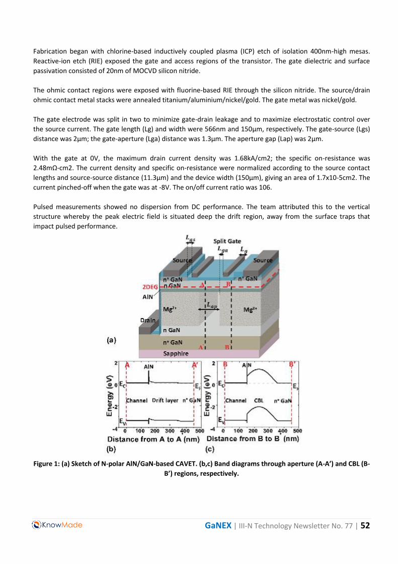
GaNEX | III-N Technology Newsletter No. 77 | 52
Fabrication began with chlorine-based inductively coupled plasma (ICP) etch of isolation 400nm-high mesas.
Reactive-ion etch (RIE) exposed the gate and access regions of the transistor. The gate dielectric and surface
passivation consisted of 20nm of MOCVD silicon nitride.
The ohmic contact regions were exposed with fluorine-based RIE through the silicon nitride. The source/drain
ohmic contact metal stacks were annealed titanium/aluminium/nickel/gold. The gate metal was nickel/gold.
The gate electrode was split in two to minimize gate-drain leakage and to maximize electrostatic control over
the source current. The gate length (Lg) and width were 566nm and 150μm, respectively. The gate-source (Lgs)
distance was 2μm; the gate-aperture (Lga) distance was 1.3μm. The aperture gap (Lap) was 2μm.
With the gate at 0V, the maximum drain current density was 1.68kA/cm2; the specific on-resistance was
2.48mΩ-cm2. The current density and specific on-resistance were normalized according to the source contact
lengths and source-source distance (11.3μm) and the device width (150μm), giving an area of 1.7x10⁻⁵cm2. The
current pinched-off when the gate was at -8V. The on/off current ratio was 106.
Pulsed measurements showed no dispersion from DC performance. The team attributed this to the vertical
structure whereby the peak electric field is situated deep the drift region, away from the surface traps that
impact pulsed performance.
Figure 1: (a) Sketch of N-polar AlN/GaN-based CAVET. (b,c) Band diagrams through aperture (A-A’) and CBL (B-
B’) regions, respectively.

GaNEX | III-N Technology Newsletter No. 77 | 53
With the gate pinched-off, the breakdown voltage (Figure 1) was 58V for a leakage of 1mA/cm2. The
researchers estimate the peak electric field at 2.9MV/cm. The researchers claim this as the “first evidence of
such a high breakdown field achieved in vertical N-polar GaN transistors.”
Figure 2: Three-terminal breakdown with the gate at pinch-off (-8V). (b) Gate dielectric breakdown test with
floating source. (c) n-CBL-n test structure measurement.
Experiments on various test structures indicated that the breakdown occurred via punch-through in the current-
block layer, not the gate dielectric. The team believes that the CBL could be improved with a more uniform,
thicker implantation profile. Thicker, lower-doped drift regions also would enable increased breakdown
voltages. The researchers say that there is progress towards growing such thicker drift regions on N-polar GaN
with lower dislocation density generation, as needed for high breakdown voltages and low leakage.
MMIC market growing at 10.6% CAGR from $7.7bn to $12.7bn by 2024 SemiconductorToday
The monolithic microwave integrated circuit (MMIC) market will grow at a compound annual growth rate
(CAGR) of 10.6% from $7.7bn in 2019 to $12.7bn by 2024, according to a report from Global Information Inc.
Factors driving growth include: increased demand from the smartphone industry; increasing adoption of E-band
frequencies to meet the growing bandwidth requirements of the space, defense and wireless communication
infrastructure sectors; and rising defense spending of countries globally.

GaNEX | III-N Technology Newsletter No. 77 | 54
Power amplifier segment to hold largest market share
Most power amplifiers are designed for a specific application producing a specific type of signal, signal
modulation scheme, and a set of specifications such as frequency range, gain (dB), gain flatness (dB), supply
voltage (VDC), power decibels (dB-milliwatt), and package type.
MMICs developed using GaN offer high input power survivability of 40dBm, potentially eliminating the
requirement for a power limiter in broadband communication, electronic warfare (EW) instrumentation or radar
applications.
Growth of this segment can be attributed to the increased use of power amplifiers in defense, automotive,
smartphone and wireless communication applications, driven by the continuously growing demand for high data
transfer rates in communication systems.
GaN material segment to grow at highest CAGR
As well as its high-brightness emission in optoelectronics, gallium nitride (GaN) is an emerging alternative to
silicon due to its high power efficiency, superior high-frequency handling capacity and its flexibility to be used
with various substrates such as silicon, sapphire and silicon carbide (SiC). Since it is a hard and mechanically
stable material with a wide bandgap and high heat capacity and thermal conductivity, MMICs developed using
GaN offer large bandwidth, improved power density and high efficiency to support the future cellular
infrastructure such as 5G for the mobile base-station transmitters.
E-pHEMT device segment to grow fastest
Enhancement-mode pseudomorphic high-electron-mobility transistors (E-pHEMTs) offer superior output power
and high efficiency with bias voltages of less than +3VDC. For commercial communication systems, E-pHEMTs
offer a combination of high gain, low noise and wide dynamic range in high-linearity MMIC applications. These
transistors can economically provide superior electrical performance in very high frequency (VHF) and ultra high
frequency (UHF) wireless communication bands commonly associated with technologies such as gallium
arsenide (GaAs) MESFETs and depletion-mode pHEMTs.
Asia Pacific to be largest market by region
Asia Pacific was the largest MMIC market by geographic region in 2018. The main growth drivers are the
expanding cellular infrastructure in the region and the increasing number of telecom equipment shipments in
countries such as China and India. Japan has been a dominant player in the global semiconductor industry since
the 1960s, while the strategy of China is to develop the highest-performance products at the lowest cost, which
has helped it gain a large share of the Asia Pacific MMIC market. The increased production of electronic devices
in the region due to the low manufacturing cost and availability of cheap labor is another growth driver. Rising
demand for smartphones, digital televisions, automobile electronics, and electro-medical devices in the Asia
Pacific region is expected to contribute to growth of the MMIC market in the region.
Key players in the MMIC market are cited as Analog Devices (USA), NXP Semiconductor (Netherlands), MACOM
(USA), Qorvo (USA), Skyworks Solutions (USA), Broadcom (USA), Infineon Technologies (Germany), Maxim
Integrated (USA), Mini-Circuits (USA), OMMIC (France), WIN Semiconductors (Taiwan), United Monolithic
Semiconductors (UMS) (France), Custom MMIC Design Services (USA), Microarray Technologies (China),
VectraWave (France), BeRex (South Korea), and Arralis (Ireland).

GaNEX | III-N Technology Newsletter No. 77 | 55
EPC: Ahead Of The Pack CompoundSemiconductor
For EPC chief executive, Alex Lidow, this year's PCIM Europe 2019 has been all about applications. Presenting
myriad enhanced-mode GaN FETs and ICs in end-products, the company is making a big play for 48 V DC-DC
power conversion in advanced computing and automotives.
“The market that we are making a full-frontal attack on, is silicon at 48 V input,” he says. “We can get higher
performance from GaN at a lower cost and with less design time... just think what it's going to be like in a few
years.”
“It's been a race and GaN has always been in front on performance but not on price,” he adds. “But now we're
in front on performance and price, and we're also accelerating; silicon's stuck in the mud.”
In recent years, EPC has been introducing ever-smaller, cheaper and higher-performing chips. Recently
delivering 100V eGaN FETs for 48V DC-DC conversion in servers and automotives, as well as automotive-
qualified 80 V eGaN FETs for lidar applications in autonomous vehicles, Lidow says device costs now rival those
of silicon chips.
“We've shrunk the die so much that, for the same ratings, we price our products at or below silicon [prices],” he
says. “Price comparisons with silicon MOSFETS at a range of performance levels show that whether we're at low
or high volumes, we're priced at the below average point.”
“And of course, the performance of GaN devices is so much superior to silicon MOSFETs at 48V,” he adds. “So
our devices are smaller and more efficient than silicon MOSFETs, yet the same price, so what's not to like?”
Market moves
With market penetration a priority, Lidow has his sights set on data-centre and automotive applications.
Following the success of the Open Compute Project - an organisation that shares designs of data-centre
products - engineers are moving to 48 V rack-level power distribution systems to boost energy efficiency of the
latest high performance computers and servers for data centres.
“We have this movement towards 48V... and today the preferred solutions are LLC-converter and buck
converter [power conversion] topologies,” highlights Lidow. “And here, I will say with all due modesty, our
products have swept all the new designs. Almost all of this is coming out of Asia, and it's a big deal for us.”
Meanwhile, the automotive industry continues its shift from 12 V to 48 V electrical distribution buses,
particularly in mild hybrid vehicles, to handle power steering, power brakes, air conditioning, suspension, high-
intensity headlamps, start-stop systems and more. What's more, new applications such as autonomous vehicles
equipped with sensors, lidar and radar are also emerging.
As such, Tier 1 automotive suppliers are busy developing 48 V electrical systems, as well as bi-directional
systems to support both 48 V and 12 V legacy accessories.
“Given all of this, automotives is huge for us,” says Lidow. “For example, the minute you go to even a mild
hybrid vehicle, you have more electrical components drawing more and more power.”

GaNEX | III-N Technology Newsletter No. 77 | 56
“We have 80 V and 100 V FETs auto-qualified for DC to DC, lidar and headlamp applications and we're also
designing into infotainment and radar systems,” he adds. “There's a heavy design effort here right now and the
market will really be starting to reach volume [production] in 2021.”
Indeed, for the EPC chief executive, the real action for GaN still lies at 400 V and lower, where the
semiconductor's high frequency and switching speeds are imperative for applications such as lidar. “[Compared
to lower voltages], the 600 V GaN market is a crowded field right now and has key vulnerabilities,” he says. “For
starters, it's not such a performance-sensitive market, and both silicon and silicon carbide are also gunning for
that 600 V node.”
At the same time, he highlights how remote control electronics are enabling the use of multi-level converters to
hit the higher voltages. Case-in-point, at this year's PCIM, EPC demonstrated a 400 V input power factor
correction circuit made from 200 V devices stacked in series.
“In this way you can pick up the higher power density at a lower cost,” he says. “So at these higher voltages, the
threats for GaN are coming in from all directions... I'm not saying this isn't a valid market but it's going to be a
difficult slog.”
So where next for EPC and GaN? In short, integration and monolithic GaN ICs.
In March this year, EPC revealed a monolithic half-bridge GaN transistor with level shifters and drivers
integrated onto the chip. The transistors are currently with alpha-customers and Lidow expects to launch
devices towards the end of this Summer.
What's more, he believes this latest IC marks the beginning of a new era for GaN power components. “Today we
see power components as transistors or diodes but I predict this [monolithic device] will redefine what a power
components is,” he says. “And I will also say that in five years, I doubt we will be launching discrete GaN
transistors at all; instead we'll be launching power products that have features and functions.”
OPTOELECTRONICS
Seoul Semiconductor files patent suit against European distributor of MEGAMAN lighting products SemiconductorToday
South Korean LED maker Seoul Semiconductor Co Ltd has filed a lawsuit in Germany in the District Court of
Düsseldorf asserting that European LED lighting distributor Leuchtstark Vertriebs GmbH is selling a ‘MEGAMAN’
brand lighting product that infringes two of its LED patents. MEGAMAN is an Asian-based LED lamp brand. Seoul
is currently investigating Leuchstark’s OEM/ODM manufacturers as well as other distributors.
The asserted patents relate to one of Seoul’s LED light extraction patent portfolios. In December, Seoul
successfully enforced a patent in the field of LED light extraction technology, and the District Court of Düsseldorf
ordered an injunction against sales of the accused Everlight products as well as a recall of any such products sold
after 13 July 2012.
Seoul holds rights to more than 14,000 LED patents, and has notified 90 companies regarding TVs, cell phones,
lighting and automobiles of patent infringements in the past year. Seoul has successfully enforced 62 patents in
eight countries in the past five years.

GaNEX | III-N Technology Newsletter No. 77 | 57
“Respecting intellectual property is essential to establish a fair competition business culture,” says Nam Ki-bum,
executive VP of the Lighting Department at Seoul Semiconductor. “We will take all necessary legal actions
against companies that have suspicions of infringing our patents or of unlawful access to our trade secret by
luring employees, as we have done against Everlight.”
Klaran launches 60mW UVC LED and reactor prototype for water disinfection SemiconductorToday
Crystal IS Inc of Green Island, NY, USA, an Asahi Kasei company that makes proprietary ultraviolet light-emitting
diodes (UVC LEDs), says that its Klaran product line has gained a new 60mW UVC LED in its water disinfection
(WD) series.
In an advanced prototype reactor, the 60mW LED has demonstrated effective and affordable water treatment
at flow rates up to three liters per minute, with disinfection rates comparable to NSF/ANSI 55 Class ‘A’, says the
firm. Klaran’s existing WD series LEDs and water treatment reactors are used to treat point-of-use (PoU) water
at flow rates up to two liters per minute and at disinfection rates comparable with NSF/ANSI Class ‘B’.
The new reactor, which is expected to be ready for market in early 2020, incorporates a user-replaceable LED
‘engine’ to address both the different market performance requirements and alternate business revenue
models of the commercial water industry. Similar to Klaran’s other WD series devices, the new LED is priced at
under 25 cents per mW. “The introduction of our new 60mW LED marks another milestone in proving that UVC
LEDs can affordably deliver the performance needs of the commercial and consumer point-of-use markets,” says
Eoin Connolly, VP for Klaran.
Klaran’s expanding portfolio of products enable manufacturers and distributors of point-of-use water products
to reduce their total cost of ownership by addressing maintenance issues, such as annual replacement and
unplanned service, related to traditional UVC technologies, says the firm. “An unplanned UV lamp failure can
quickly cost hundreds of dollars to a service provider, making a serious impact on profit margins,” notes
Connolly. “Our rigorous testing of thousands of Klaran devices and ISO 9001 quality system provide the data-
driven proof in the reliability and performance of our Klaran products,” he adds.
GaNEX | III-N Technology Newsletter No. 77 | 58
Indium gallium nitride platelets for green and red light-emitting diodes SemiconductorToday
Lund University and RISE Research Institutes in Sweden have developed indium gallium nitride (InGaN) platelet
arrays as a basis for green and red light-emitting diodes (LEDs) [Zhaoxia Bi et al, Nano Lett., published online 2
April, 2019]. The researchers used the platelets to achieve quantum well (QW) regions with higher indium
content with less compressive strain from lattice mismatching. “The large strain has a direct impact on the
crystal quality of the QWs, potentially introducing plastic crystal deformation during growth and then leading to
a dislocation formation,” the team explains.
High strain in InGaN heterostructures also leads to large piezoelectric fields, which reduce the efficiency of the
electron-hole recombination processes that are needed for photon emission – a mechanism called the
‘quantum-confined Stark effect’ (QCSE).
Strain effects severely reduce the performance of red and green InGaN-based LEDs, relative to blue devices that
can reach 80% external quantum efficiency. By using the InGaN platelets, lower strain in InGaN QWs with high
indium content should be achieved due to the smaller lattice mismatch. Higher indium content narrows the
bandgap, increasing the wavelength.
The platelet growth technique combined selective-area metal-organic vapor phase epitaxy (MOVPE) and
reformation to convert InGaN pyramid structures into c-plane oriented platelets. The selective-area epitaxy was
on (0001) GaN-on-silicon templates, using silicon nitride masking with 100nm-diameter holes at 1μm pitch. The
platelets are 100-200nm high and extend laterally a few hundred nanometers.
The reformation process consisted of 1070°C annealing in ammonia (NH3) and InGaN regrowth to create a
smooth top surface. The annealing did not affect the {10-11} pyramid side facets, which remained smooth after
the thermal processing.
The researchers explain: “The surfaces of {10-11} planes are N-terminated. N atoms at the surface are supposed
to bond with H atoms cracked from NH3, which can be a reason for the stable {10-11} planes during the
annealing.”
The regrowth included an intermediate InGaN layer with a low V/III ratio of 700 (close to the limit for In/Ga
droplet formation). The aim of the intermediate layer was to reduce pit formation in the c-plane surface. The
researchers suggest that the metal-rich conditions on the growth plane gives a longer adatom diffusion length,
flattening the initially rough surface.
The indium content of the intermediate layer was estimated to be less than 5%. The technique was successful in
removing pits from In0.09Ga0.91N platelets, but there remained some pits in In0.18Ga0.82N structures. This
residual pitting was attributed to the larger lattice mismatch with the intermediate layer. The top InGaN layer
was 40-50nm thick.
Comparison of photoluminescence and energy-dispersive x-ray analysis suggested that the InGaN below the
intermediate layer had higher indium content fluctuations compared with the InGaN above. Photoluminescence
analysis tends to overestimate indium content when there are large fluctuations.
The researchers found that growth of InGaN quantum wells on the InGaN platelets had enhanced indium
incorporation, probably due to reduced compressive strain relative to wells grown on pure GaN.

GaNEX | III-N Technology Newsletter No. 77 | 59
The InGaN platelets had narrow photoluminescence peaks: 107meV and 151meV full-widths at half-maximum
(FWHMs) for In0.09Ga0.91N and In0.18Ga0.82N, respectively. These platelets were used for green and red LEDs,
respectively.
Figure 1: (a, e) Cross-sectional high-angle annular dark-field scanning transmission electron microscope
(HAADF-STEM) images of single QW samples. The white arrow in panel e indicates dislocation. (b, f) Magnified
HAADF-STEM images close to periphery and (c, g) high-resolution TEM images in middle of QWs. (d, h) CL
spectra measured at 10K. Inset: SEM images and corresponding monochromatic CL images with QW emission.
CL images recorded in energy windows of (d) 1.80−2.50eV and (h) 1.85−2.35eV.
Cathodoluminescence (CL) spectra under electron-beam excitation showed a QW peak in the emission at 2.17eV
(in the yellow range) for the In0.09Ga0.91N platelet and 1.95eV (red) for In0.18Ga0.82N (Figure 1). The
researchers report that the QW was slightly thicker on an In0.18Ga0.82N platelet – 5.8nm, compared with
4.5nm. The team suggests the thicker well increases the quantum-confined Stark effect, red-shifting the
emission.
The indium content of the well could also be higher on the higher-indium-concentration platelet, narrowing the
bandgap. The higher indium content could be the result of reduced ‘indium pulling’ compared with the lower-
indium-concentration platelet.
For LEDs, a ~200nm p-InGaN contact layer was added to platelets with quantum wells (Figure 2). The n-contact
was through the n-GaN buffer. Electrical isolation was achieved with 30nm atomic layer deposition (ALD)
aluminium oxide (Al2O3) passivation and spin-coated/planarized polymer spacer material. The spacer was also
used as an etch mask for removal of the Al2O3 from the top of the p-GaN contact. The contact metal was
circular in form with 360μm diameter, covering around 1.2x10⁵ platelets.

GaNEX | III-N Technology Newsletter No. 77 | 60
Figure 2: (a) Schematic of InGaN platelet LEDs. (b, c) EL spectra obtained at different current injection levels
for green and red LEDs on In0.09Ga0.91N and In0.18Ga0.82N platelets, respectively. Current density
normalized to QW rather than contact area.
Electroluminescence (EL) from the LEDs gave green (2.30eV) and red (1.98eV) peaks for In0.09Ga0.91N and
In0.18Ga0.82N platelet structures, respectively. The corresponding FWHM linewidths were 210meV and
150meV.
Osram launches its first quantum dot LED SemiconductorToday
In booth #1701 at the LIGHTFAIR International 2019 trade show in Philadelphia, PA (19–23 May), Osram Opto
Semiconductors GmbH of Regensburg, Germany is showcasing its first quantum dot (QD) LED.
Due to their very small size, the light that is re-emitted when blue LED light hits nanoparticles depends on their
size: QD particles that are roughly 3nm in size produce green light, while particles about 7nm emit red light.
Osram is using such tunable light conversion technology for the first time in its new Osconiq S 3030 QD mid-
power LED, which will lead to more QD LEDs for the general lighting market in the future. The Osconiq S 3030
QD was specially developed to enable users to design luminaires with high efficacy and color rendering for area
lighting and downlight applications.
When manufacturing conventional white LEDs, the main objectives are efficacy and product quality. Achieving
both at the same time is particularly challenging, especially with very high color rendering indexes (CRI), says
Osram. The advantage of using quantum dots is that the existing LED manufacturing processes remain the same.
QDs are simply used instead of conventional phosphors when the converter material is applied.
More than a year ago, Osram acquired Pacific Light Technologies (PLT), which develops and manufactures
optical nanomaterials. Osram says that the PLT QD technology is enabling it to begin to close the efficacy gap
that exists between CRI 80 and CRI 90 LEDs today. The new Osconiq S 3030 includes a specially developed QD
phosphor solution that enables CRI 90 to achieve an efficacy value of 173lm/W at 3000K – which is claimed to

GaNEX | III-N Technology Newsletter No. 77 | 61
be a best-in-class value for 0.2W high-performance LEDs. The compact dimensions of 3.0mm x 3.0mm and the
low thermal resistance enable simple system design. The Osconiq S 3030 QD is also available in various color
temperatures, from 2700 to 6500K.
Osram says that another unique feature of the PLT QD technology is that the quantum dots are encapsulated to
protect them from moisture and other external influences that pose the greatest risk to the functionality of an
LED. The special encapsulation technology allows the QDs to reliably master the demanding conditions of on-
chip operation within the LED component, the firm adds.
Plessey enters into long-term micro-LED supply agreement with Vuzix SemiconductorToday
An exclusive display device design and long-term supply agreement will support the development and
production of next-generation augmented reality (AR) products and solutions combining the micro-LED light
source technology of UK-based Plessey with the expertise and IP in smart glasses and essential optics
technologies of Vuzix Corp of Rochester, NY, USA.
Vuzix has already developed an evolving family of smart glasses culminating in the Vuzix Blade, a next-
generation smart display with a see-through viewing experience via its proprietary waveguide optics. Formed
from glass with precision nanostructures, the waveguide enables users to see high-resolution computer-
generated graphics, images and information superimposed over images from the physical or real world.
Plessey says that its micro-LED solution will simplify existing smart glasses’ complex optical system of red, green
and blue light sources and their additional optics by replacing it with a single self-emitting display that has
integrated micro-optical elements. Size, weight and power reduction are key considerations in the AR wearables
market. Existing light source systems have considerable losses all the way through to the waveguide and the
optical systems around them are bulky and complex, whereas an emissive micro-LED has simple optical
requirements, allowing a much smaller footprint with minimal system losses by placing the light source directly
in front of the waveguide.
“Micro-LED technology represents a key part of the solution needed to bring the form and functionality of Vuzix
next-generation smart glasses to the look and feel of fashion forward glasses,” believes Vuzix’s president & CEO
Paul Travers.
“By overcoming the difficulties of manufacturing micro-LEDs on a commercial scale, Plessey is playing a central
role in providing next-generation technology to the augmented reality and display markets,” says Plessey’s
president of corporate and business development Mike Lee.
Ultraviolet aluminium gallium nitride shell nanowire light-emitting diodes SemiconductorToday
The National Institute of Standards and Technology (NIST) and University of Colorado in the USA have reported
aluminium gallium nitride/gallium nitride (AlGaN/GaN) shell/core nanowire light-emitting diodes (LEDs) that
demonstrated ~5x the light output compared with GaN/GaN nanowire devices [Matt D Brubaker et al,
Nanotechnology, vol30, p234001, 2019].
Developing ultraviolet LEDs such as the 365nm wavelength from the AlGaN/GaN device are seen as being useful
for spectroscopy, photopolymer curing, water purification and medical disinfection. Some of these applications
need short ‘deep’ UV wavelengths less than 300nm. Nanowire structures might be useful in boosting the pitiful
efficiencies (mostly less than 10%) in high-aluminium-content AlGaN LEDs based on conventional technology.

GaNEX | III-N Technology Newsletter No. 77 | 62
First, ordered arrays of nanowires were grown using plasma-assisted molecular beam epitaxy (PAMBE) on
nitrogen-polar GaN/AlN templates on (111) silicon with a silicon nitride mask. The holes in the mask for
nanowire growth were 80-240nm diameter with 300-10,000nm pitch. The silicon-doped n-GaN cores were
grown at 860°C substrate temperature. The core length was around 2μm. The ~40nm-thick silicon-doped
Al0.09Ga0.91N shell was grown at 700°C.
Photoluminescence spectra measured at 5K suggested that the Al mole fraction of the shell tip decreased with
nanowire diameter. By contrast, reducing the pitch increased Al concentration. The decrease in Al content at the
nanowire tip was related to reduced mobility of the atoms at the growing tip, compared with Ga.
The Al content of the main shell of the nanowire stems was more difficult to determine, probably due to non-
radiative recombination, surface states and defects. The researchers used emissions from excitons (bound
electron-hole states) to estimate Al content. Smaller-diameter nanowires were found to have higher-Al-content
shells. Smaller pitch arrays had low Al concentration.
The nanowire growth process was modified to include doping for p-i-n LEDs. The n-GaN core region was grown
to a height of 3.3μm pitched at 5μm. Shell growth was initiated with 15nm n-GaN followed by ~85nm intrinsic
AlGaN, ~285nm p-AlGaN and ~5nm heavily doped p++-AlGaN.
The LED p-contact electrode was constructed by 20nm/200nm nickel/gold deposition at normal incidence,
followed by 200nm gold at 45°. This covered one side of the wires with metal while the other side allowed light
extraction. The n-side current flow was through the buffer with electrical isolation provided by the silicon nitride
nanowire growth mask.
Figure 1: Core–shell p–i–n nanowire LED characteristics comparing AlGaN/GaN heterojunctions and GaN/GaN
homojunctions. (a) Scanning electron micrograph of post-metallization AlGaN/GaN core–shell LEDs, with inset
pre-metallization single nanowire. (b) Current-voltage characteristics and (c) EL spectra for 25 nanowire LEDs.
(d) EL images for 4 nanowire LEDs are shown in the figure. GaN p–i–n EL intensities multiplied by factor of
three. (e) Peak emission wavelength and (f) integrated intensity versus current for various core diameters.

GaNEX | III-N Technology Newsletter No. 77 | 63
The researchers compared the performance of the AlGaN/GaN heterojunction LEDs with GaN/GaN
homojunction nanowire devices previously reported by the group (Figure 1). The turn-on voltage of the
AlGaN/GaN LEDs was higher than for GaN/GaN, “likely related to the reduced electron overflow current and
increased barrier to hole injection expected for higher Al mole fractions,” according to the team.
Subjecting the AlGaN/GaN LED to prolonged current injection seemed to have an electrical annealing effect on
the p-contact, giving increased electroluminescence (EL) intensity and lower series resistance. The researchers
comment: “Further development of optimized p-contact metallization and annealing processes are expected to
reduce burn-in effects and improve overall device performance.”
The EL from the AlGaN/GaN was around 365nm wavelength, close to the band edge of GaN. This was in contrast
to the GaN/GaN LEDs, which emitted around 380nm, corresponding to donor-acceptor-pair (DAP)
recombination from electrons injected into the p-GaN shell, according to the researchers. The team also
suggests that GaN core emissions could be reabsorbed in the GaN shell, unlike with the wider-bandgap AlGaN.
The 380nm emission and 365nm reabsorption effects are stopped by the wider-bandgap AlGaN, which is also
commonly used as an electron-blocking layer in standard GaN LEDs. The researchers report that the integrated
EL intensity in the AlGaN/GaN nanowire LEDs was around 5x that of the GaN/GaN reference for a given current
injection.
Leti develops CMOS-driven micro-LEDs with simplified transfer process that eliminates TFT backplane SemiconductorToday
On 14 May during Display Week 2019 in San Jose, CA, USA, micro/nanotechnology R&D center CEA-Leti of
Grenoble, France has presented a paper on new technology for fabricating high-performance gallium nitride
(GaN) micro-LED displays for applications ranging from smart watches to TVs with no size limit.
The approach fabricates elementary units of all-in-one red, green, blue (RGB) micro-LEDs on a CMOS driving
circuit, and transfers the devices to a simple receiving substrate. The units are fabricated with a full
semiconductor, wafer-scale approach.
“This new process, in the proof-of-concept stage, paves the way to commercial, high-performance micro-LED
displays,” reckons François Templier, CEA-Leti’s strategic marketing manager for photonic devices. “The CMOS-
based approach provides higher-brightness and higher-resolution micro-LEDs and is a game changer for very
large TVs,” he adds.
While they promise exceptional image quality and better energy efficiency than existing liquid crystal display
(LCD) and organic light-emitting diode (OLED) technologies, micro-LED displays currently face significant barriers
to commercialization.
One of the biggest challenges is improving the performance of the driving electronics, which require more
power to deliver brighter images and more speed to support continuously increasing demands for high display
resolution. Faster electronics are required to power millions of pixels in a fixed-frame time in micro-LED
displays, but existing thin-film transistor (TFT) active-matrix driving display technology cannot provide the
necessary current and speed.
CEA-Leti’s new approach fabricates CMOS-driven, high-performance GaN micro-LED displays with a simplified
transfer process that eliminates the use of the TFT backplane. RGB micro-LEDs are stacked directly onto a micro-

GaNEX | III-N Technology Newsletter No. 77 | 64
CMOS circuit, and each unit is transferred onto a simple receiving substrate. Then, the RGB micro-LEDs and the
backplane are fabricated on a single semiconductor line.
In addition to increasing power and driving speed – and improving display performance – this process avoids
several costly steps needed with existing technology to make electrical and mechanical contacts between micro-
LEDs and the receiving substrates.
New technique could pave way to simple color tuning of monolithically integrated GaN LEDs SemiconductorToday
A team at Lehigh University, West Chester University, Osaka University and the University of Amsterdam has
demonstrated a new technique that could enable simple color tuning of gallium nitride (GaN)-based LEDs simply
by changing the time sequence at which the operating current is provided to the device (ACS Photonics, ‘Color-
Tunablility in GaN LEDs Based on Atomic Emission Manipulation under Current Injection’).
Notably, the technique is compatible with current LEDs that are at the core of commercial solid-state LED
lighting. “This work could make it possible to tune between bright white and more comfortable warmer colors in
commercial LEDs,” says Volkmar Dierolf, Distinguished Professor and Chair of Lehigh’s Department of Physics,
who worked on the project.
Lead author Brandon Mitchell is a former graduate student in Dierolf's lab, now an assistant professor in the
Department of Physics and Engineering at West Chester University in Pennsylvania.
In existing active LED displays, different colors are produced by three to four individual LEDs placed close to
each other that create the different fundamental colors needed to produce the full color spectrum.
“We demonstrate that this can be achieved by a single LED,” says Dierolf.
“We show that is possible to attain red, green and blue emissions originating
from just one GaN LED structure that uses doping with a single type of rare-
earth ion, europium (Eu),” he adds. “Using intentional co-doping and energy-
transfer engineering, we show that all three primary colors can emit due to
emission originating from two different excited states of the same trivalent
Eu3+ ion (620nm red/orange and 545nm green) mixed with near-band-edge
emission from GaN centered at ~430nm (blue/violet). The intensity ratios of
these transitions can be controlled by choosing the current injection
conditions such as injection current density and duty cycle under pulsed
current injection.”
In other words, the team achieved color-tunability in a single GaN-based LED through the manipulation of the
emission properties of an atomic-type dopant.
Graphic: Top row is a GaN:Eu LED, which can be tuned from red-yellow due to red and green light mixing from
different Eu states. Middle and bottom rows are of a GaN:Eu LED with additionally added Si/Mg, which adds
blue emission. Each picture is under a different current injection/filtering condition. Credit: West Chester
University.
“The main idea of this work - the simultaneous active exploitation of multiple excited states of the same dopant
- is not limited to the GaN:Eu system, but is more general,” notes Mitchell. “The presented results could open up
a whole new field of tunable emission of colors from a single dopant in semiconductors, which can be reached
by simple injection current tuning,” he adds.

GaNEX | III-N Technology Newsletter No. 77 | 65
The research could benefit those looking for more comfortable ‘warmer’ white light from LEDs. “It could pave
the way for monolithic integration for simple color tuning of a light bulb,” says Dierolf. “It would also be
beneficial for micro-LED displays, since it allows for higher density of pixels.”
The materials used in previous research on color tunable LEDs did not allow for easy integration with current
LED technology, he adds. This work is compatible with existing GaN-based LEDs that are at the core of
commercial solid-state LED lighting.
Rise of LED Lighting For Cars Driven By Energy Efficiency CompoundSemiconductor
The approximately $35 billion market for automotive lighting is estimated to see just under 5 percent year on
year growth in 2019, according to a new report by Future Market Insights. While passenger cars have
significantly driven the LED Automotive Lighting Sales, bright prospects have been foreseen for sales in electric,
in line with the rising trend of vehicle electrification.
Nearly 60 percent of the automotive lighting systems installed are of headlights/front lights, which collectively
capture more than 3/4th of the market revenue, with rear lights. Fog lights are gradually gaining ground in front
and rear lighting systems, which is likely to shape the overall performance of automotive lighting market, as
indicated by the report.
Lightweight automotive components have been a trendsetter over the past decade, will push the demand
growth of lightweight automotive lighting in parallel. This growth forecast is predominantly owing to increasing
vehicle electrification and surging demand for high-performance, fuel efficient vehicles.
Halogen lamps continue to reign supreme, holding more than 65 percent share in the automotive lighting
market. In line with tightening vehicle emission standards that demand reduced weight and improved fuel
efficiency, the automotive lighting market will observe strong emergence of LED. Superior endurance and high
energy efficiency are projected to provide an impetus to LED popularity over halogen and HID counterparts. The
report envisages a preeminent push to LED automotive lighting from manufacturers of premium class vehicles.
Enhanced aesthetic appeal of vehicles with innovative lighting features will remain a priority strategy for leading
automakers and OEMs. However, lighting technology innovators in collaboration with prominent market players
are also strategizing on introducing economic range products, which is cited as another factor providing a strong
push to LED automotive lighting products.
While compact and mid-size passenger car manufacturers remain prime consumer of automotive lighting
solutions, the report indicates that this demand growth will be spectacular in EVs over the coming years. Hybrid
EVs will further account for a considerable demand share in automotive lighting market. Moreover, billowing
sales of motorcycles, particularly in developing economies, will bolster installations of a wide range of
automotive lighting in the two-wheelers segment, says the report.
In a fairly consolidated competitive landscape of automotive lighting market, a majority of players are based in
North America, Europe, and China. Automotive lighting market leaders such as Koito Manufacturing, Valeo SA,
Magneti Marelli, Hella, and Stanley Electric continue to dedicate a majority of investments in strategic
acquisitions and new product launches.
Valeo recently acquired a Japanese automotive lighting manufacturer, Ichikoh Industries, Ltd. Expansion has
also been among the key developmental strategies in the competitive landscape of automotive lighting market.
On the other side, Tier 2 companies including Osram, Varroc Group, Robert Bosch, LG Lightings, and Hyundai

GaNEX | III-N Technology Newsletter No. 77 | 66
Mobis are focusing on collaborative ventures that prominently target product innovations and new launches in
automotive lighting space.
In the latter half of 2018, Fiat Chrysler Automobiles inked a collaborative agreement over the sale of their
automotive components business - Magneti Marelli to the Japanese supplier CK Holdings. (Calsonic Kansei
Corporation's holding company). Osram has been actively introducing new automotive lighting product lineups
in the market.
While Europe retains the top consumer title in automotive lighting landscape, the report projects significant
growth potential for automotive lighting market in emerging Asian countries. Automakers, OEMs, and other
lighting product manufacturers will capitalise on a series of untapped opportunities particularly in East Asian
market, attributed to soaring automotive sales, elevating acceptance for EVs and HEVs, and more importantly,
improving purchasing power of consumers. East Asia is likely to represent just-under a third of the global
automotive lighting market value, towards 2019 end.
OTHER
Newport Wafer Fab completes multi-million-pound refinancing deal to new fund equipment and plant SemiconductorToday
Newport Wafer Fab (NWF), the UK’s 200mm compound semiconductor wafer foundry, has completed a multi-
million pound refinancing deal, involving a restructure of existing Welsh Government loans and a new asset
finance facility from HSBC UK.
The deal includes the early settlement of deferred
consideration, the purchase of specialist back-end-of-line
equipment to broaden the foundry’s manufacturing
capabilities, and a £3m contribution to a new combined
heat and power (CHP) plant designed to reduce utility
costs by over £1.5m per annum.
NWF was acquired by private investors in September 2017
from Germany’s Infineon Technologies AG (which
acquired the fab on buying US-based International
Rectifier Corp at the beginning of 2015).
NWF is a critical component of CS Connected, the world’s first compound semiconductor cluster. CS Connected,
which is supported by investment from the Welsh and UK governments and the Cardiff Capital Region (CCR),
brings together compound semiconductor material expertise and large-scale semiconductor wafer
manufacturing, combined with academic research, to deliver bespoke solutions to customer using compound
semiconductor materials.
NWF provides volume manufacturing services for the cluster and any customers who have developed their own
products using silicon and compound semiconductors on silicon. It is said to be pivotal to a number of significant
international projects being scrutinised by companies attracted to the one-stop-shop capability of CS
Connected.

GaNEX | III-N Technology Newsletter No. 77 | 67
CS Connected is one of 24 shortlisted projects (and the only one wholly based in Wales) to receive early-stage
funding from the ‘Strength in Places’ Fund of UK Research and Innovation (UKRI) to develop a full-stage business
case submission, benefiting all regions of the UK by enabling them to tap into research and innovation capability
spread across the country, aiming to yield significant economic impact, high-value job creation and regional
growth.
NWF’s CEO Dr Paul James expressed his gratitude to the involved parties for their continuing support that has
strengthened the position of NWF and the wider CS Cluster.
“The Welsh Government has invested significantly in establishing Wales as a global centre for advanced
compound semiconductor technologies and we were pleased to provide support for Newport Wafer Fab so that
they can continue work to attract further commercial investment,” says Ken Skates, the Welsh Government’s
Minister for Economy and Transport. “The cluster and its skilled workforce is hugely important to our economy
and, with world-leading companies and technologies operating and thriving in the region, I look forward to its
continued success and growth in the years ahead,” he adds.
“We are delighted to be supporting a business in growth and one which is helping retain a number of jobs in
South Wales,” comments Warren Lewis, head of corporate banking in South Wales at HSBC UK. “The funding
from HSBC UK is helping NWF grow its customer base both domestically and internationally and, as a result, is
on the path to becoming the largest semiconductor foundry in Europe. We look forward to continuing our
support over the coming years,” he adds.
“The Cardiff Capital Region is committed to creating a complete compound semiconductor eco-system in South-
East Wales to take advantage of the growing prominence of compound semiconductor technologies,” says
Councillor Andrew Morgan, leader of Rhondda Cynon Taf County Borough Council, and chair of the Cardiff
Capital Region’s Regional Cabinet. “We are supporting the establishment of the world’s first compound
semiconductor cluster. In turn, this can place this region at the heart of a sector which is developing technology
which is playing an increasingly vital role in the way we live,” he adds.
“To achieve our aspiration to create the world’s first compound semiconductor cluster, a robust and sustainable
supply chain is critical,” states Councillor Debbie Wilcox, leader of Newport City Council, and a member of the
Cardiff Capital Region’s Regional Cabinet. “This investment will enable support of this, and in the process deliver
the economic and social benefits we aspire to achieve for our local communities here in South-East Wales.”
GlobalFoundries sign long-term agreements for high-volume supply of Soitec’s 300mm SOI wafer SemiconductorToday
GlobalFoundries (GF) of Santa Clara, CA, USA (one of the world’s largest semiconductor foundries, with
operations in Singapore, Germany and the USA) and Soitec of Bernin, near Grenoble, France - which makes
engineered substrates including silicon-on-insulator (SOI) wafers - have signed multiple long-term high-volume
supply agreements for 300mm SOI wafers to meet the growing demand for GF’s differentiated radio-frequency
silicon-on-insulator (RF-SOI), fully depleted silicon-on-insulator (FD-SOI) and silicon photonics technology
platforms. The firms say that the agreements build on the existing close relationship between them to ensure
high-volume manufacturing for years to come.
RF-SOI solutions are used in all smartphones manufactured today and FD-SOI has become the standard
technology for cost-effective, low-power devices in high-volume consumer and Internet of Things (IoT)
applications as well as for mission-critical safety solutions in automotive proximity sensing. Silicon photonics

GaNEX | III-N Technology Newsletter No. 77 | 68
technologies enable solutions to support the massive growth in communication infrastructure for data centers
and next-generation 5G communication optical networks.
“GF is delivering and investing in highly differentiated industry-leading technologies required for 5G, IoT, data-
center and automotive applications,” says Bami Bastani, senior VP of business units at GF. “These long-term
agreements with Soitec, a valued partner, represent our commitment to ensure a secure supply of ultra-lower-
power, high-performance SOI solutions and supply that meet customers fast-growing needs and unprecedented
demand in these attractive markets,” he adds.
“GF is leading the industry in providing differentiated SOI solutions, creating more demand for Soitec's
engineered substrates,” comments Soitec’s CEO Paul Boudre. “These agreements reflect the strength of our
long-term partnership as we build the required capacity to meet this growing SOI demand.”
Element Six launches diamond thermal-material-grade Diafilm TM220, offering thermal conductivity over 2200W/mK SemiconductorToday
In booth 1190 at the International Microwave Symposium (IMS 2019) in Boston, MA, USA, Luxembourg-
registered synthetic diamond materials firm Element Six (E6, part of the De Beers Group) is launching the
diamond thermal-material-grade Diafilm TM220, which is claimed to be the first diamond thermal material
engineered to offer industrial users thermal conductivity in excess of 2200W/mK.
The launch is in response to the ever-increasing demand for more content and bandwidth, which is pushing the
boundaries of semiconductor thermal management. The shift to higher frequencies is creating a unique
opportunity for chemical vapor deposition (CVD) diamond, and Element Six says that the launch extends its
portfolio of thermal materials to even higher heat-spreading capabilities.
The new grade of CVD diamond thermal material is suitable for the thermal management of high-power-density
radio frequency (RF) and application-specific integrated circuits (ASIC) devices, as well resistive components for
power management at high frequencies. Diafilm TM220 also has applications in gallium nitride (GaN)-based RF,
in addition to monolithic microwave integrated circuits (MMICs) for phase-array radar, space and satellite, 5G
base stations and beyond. Moreover, the success of terabit rate optoelectronics networks for both metro and
long-haul content delivery is predicated on high-efficiency thermal management.
As with the other material grades of Diafilm TM, TM220 is thermally isotropic, spreading heat with equal
efficiency in a planar direction as well as through the material. Additional Diafilm TM220 properties include
dielectric permittivity, optical clarity, electrical insulation, low density and chemical inertness, making it suitable
for pushing the boundaries of advanced thermal management as either an active or passive component, says
the firm.
“This new material validates the unique multi-functionality of CVD diamond and further demonstrates Element
Six’s leadership and innovation in CVD diamond synthesis and material characterization, where we continue to
open up new areas of advancement,” says Speaking at IMS, Thomas Obeloer, business development manager
for Thermal Applications. “We have already had positive feedback from customers in RF device packaging, x-ray
generation and the high-performance ASIC sector, who were early adopters of the TM220 grade,” he adds.
Material blanks of Diafilm TM220 are available in standard thicknesses and can be made to meet specific
customer requirements. To match the high performance of the diamond, the use of high-quality, sputter-

GaNEX | III-N Technology Newsletter No. 77 | 69
deposited thin-film metallization is offered, and specifications to meet advanced needs for wire bonding or
direct deposition of solder materials onto the CVD diamond can be supplied.
Qorvo cuts June-quarter financial guidance due to US action against Huawei SemiconductorToday
In response to the US Department of Commerce’s Bureau of Industry and Security (BIS) adding Huawei
Technologies Co Ltd and 68 of its affiliates to its ‘Entity List’ prohibiting the sale to Huawei of products covered
by the Export Administration Regulations (EAR) without obtaining an appropriate export license, Qorvo Inc of
Greensboro, NC, USA has updated the financial guidance it provided on 7 May for its fiscal first-quarter 2020 (to
end-June 2019) and full-year 2020.
Sales from its Mobile Products (MP) and Infrastructure and Defense Products (IDP) operating segments to
Huawei and its affiliates accounted for about $469m (15%) of Qorvo’s total revenue in its fiscal full-year 2019
(ended 30 March). Qorvo is continuing to review the impact of the BIS action on its business, including its ability
to apply for and obtain licenses to allow it to ship products to Huawei in the future. Pending further
developments, Qorvo has ceased shipments to Huawei and its affiliates and cannot predict when it will be able
to resume such shipments.
In the meantime, Qorvo is cutting its fiscal first-quarter 2020 guidance for non-GAAP revenue from $780-800m
to $730-750m, for gross margin from 45-45.5%, and for diluted earnings per share from $1.30 to $1.15.
Currently, for fiscal second-quarter 2020, Qorvo’s assumes no sales to Huawei and is projecting revenue to be
roughly flat sequentially. However, due to the ongoing uncertainty of this situation, the firm is not providing any
additional update to its fiscal 2020 guidance at this time.
Cree chosen as silicon carbide partner for Volkswagen’s FAST program SemiconductorToday
Cree Inc of Durham, NC, USA has been selected as the exclusive silicon carbide (SiC) partner for Volkswagen
Group’s ‘Future Automotive Supply Tracks’ initiative (FAST). The aim of FAST is to work together to implement
technical innovations more quickly than before and to realize global vehicle projects more efficiently and
effectively.
“The Volkswagen Group has committed to launch almost 70 new electric models in the next ten years, which is
up from our pledge of 50 and increases the projected number of vehicles to be built on the group’s electric
platforms from 15 million to 22 million in that timeframe,” says Michael Baecker, head of Volkswagen
Purchasing Connectivity. “An effective network is our key to success,” he adds. “Our FAST partners are our
strategic partners, each of them outstanding in their respective field.”
Cree’s CEO Gregg Lowe with Michael Baecker, head of Volkswagen Purchasing Connectivity during Volkswagen
Group’s FAST partner selection ceremony in Wolfsburg, Germany.
Photograph: Cree’s CEO Gregg Lowe with Michael Baecker, head of Volkswagen Purchasing Connectivity during
Volkswagen Group’s FAST partner selection ceremony in Wolfsburg, Germany.
The agreement connects two simultaneous revolutions: the automotive industry’s move from internal
combustion engines to electric vehicles (EVs) and the growing adoption of silicon carbide in the semiconductor
market. It should also drive innovation for both parties.

GaNEX | III-N Technology Newsletter No. 77 | 70
The use of silicon carbide accelerates the automotive industry’s transformation to electric vehicles, enabling
greater system efficiencies that result in electric cars with longer range and faster charging, while reducing cost,
lowering weight and conserving space.
“Cree’s technology is at the heart of the dramatic change underway in EVs, and we are committed to supporting
the automotive industry as it transitions to more efficient, higher-performing SiC-based solutions,” says Cree’s
CEO Gregg Lowe. “VW Group is a global power in the automotive field with a strong commitment to electric
vehicles, and this partnership will leverage the advantages of silicon carbide to enable longer driving distances,
shorter charge times and improved efficiency,” he adds.
Volkswagen Group and Cree will be working with tier-one and power module suppliers to engineer SiC-based
solutions for future Volkswagen Group vehicles. The partnership was announced on 10 May. This follows Cree’s
announcement on 7 May that it is expanding its manufacturing capacity for silicon carbide MOSFETs and wafers.
PowerAmerica Updates WBG Roadmap CompoundSemiconductor
PowerAmerica has unveiled an updated technology roadmap to provide a common vision of the future for the
WBG (wide bandgap) community to work toward.
This roadmap outlines key markets and application areas as well as the performance targets GaN and SiC
technologies are expected to meet over time, technical barriers to achieving those targets, and activities needed
to overcome those barriers.
While WBG technologies such as SiC and GaN offer significant capabilities for power electronics, industry must
overcome numerous challenges including high material and manufacturing costs, reliability perceptions,
packaging and performance requirements, and difficulty coordinating efforts across the entire power electronics
ecosystem.
Recent progress against these challenges in automotive applications, PV inverters, and power supplies is
encouraging; however, SiC and GaN have not taken off as rapidly in traction applications, industrial motor
drives, and wind turbines. Further strides are needed to begin manufacturing these devices at high volumes and
competitive costs across the full range of useful applications.
The following high-level recommendations are a summary of the actions found PowerAmerica's 5- Year
Roadmap Strategy.
Reducing Cost
- Lower the $/ampere of WBG devices and power modules.
- Support vertically integrated fabrication.
- Support and promote early adopter, high-volume WBG applications.
- Establish SiC and GaN open foundries to scale to high-volume manufacturing.
Improving Reliability and Quality
- Establish WBG power electronics reliability at system-level and investigate degradation/failure mechanisms of
devices, modules, or systems.
- Develop open databases for reliability data.
- Develop capability to perform AECQ or JEDEC standard tests for WBG power devices.
-Set dedicated standards for WBG power electronics.

GaNEX | III-N Technology Newsletter No. 77 | 71
Enhancing Performance Capabilities
- Focus on near-term applications to demonstrate the system-level advantages of WBG power devices.
- Support pathways to commercialisation for industry-led projects.
- Promote reference designs, advanced gate drives and modules, and work in advanced peripherals.
Strengthening the Power Electronics Ecosystem
- Continue to offer the Device Bank for quick access to SiC and GaN devices.
- Continue to provide communication mechanisms for different levels of stakeholders, from vendors to end
users.
- Train a WBG power electronics workforce.
- Monitor basic core technologies, state-of-the-art complementary technologies, and long-term applications to
identify promising opportunities.
A more detailed version of the roadmap, available to members only, outlines key markets and application areas
for SiC and GaN power electronics, the performance targets GaN and SiC technologies are expected to meet
over time, technical barriers to achieving those targets, and activities needed to overcome those barriers.

GaNEX | III-N Technology Newsletter No. 77 | 72
PATENT APPLICATIONS
More than 300 new patent families (inventions) were published in May 2019.
Other patent applicants Anhui East China Photoelectric Technology Research Institute, Beijing University of Technology, Cea - Commissariat à l’Energie Atomique Et Aux Energies Alternatives, Changchun Institute of Optics Fine Mechanics & Physics Chinese Academy of Sciences, China United Northwest Institute For Engineering Design & Research, Dongtai Gaoke Equipment Technology, Fudan University, Fuji Electric, Guangdong Midea Refrigeration Equipment, Infineon Technologies, Infineon Technologies Austria, Institute of Electronic Engineering China Academy of Engineering Physics, Institute of Microelectronics Chinese Academy of Sciences, Intel, Jiangsu Dahang Hongcheng Power Electronics, Lattice Power, Midea, Nanjing University, Nikkiso, Northwestern Polytechnical University, NXP, Panasonic, Sciocs, Shaanxi Reactor Microelectronics, Shanghai Jiao Tong University, Shanghai Xinsheng Semiconductor Technology, Sharp, Shenzhen Original Digital, Sumitomo Chemical, Sun Yat Sen University, University of California, UV Craftory, Wisconsin Alumni Research Foundation, Wuhan University, Xiangneng Hualei Optoelectronic Corppration, Zhangjiagang Ever Power Semiconductor, Advanced Optoelectronic Technology, AGC, Anhui Sanan

GaNEX | III-N Technology Newsletter No. 77 | 73
Optoelectronics Technology, Anhui University of Technology, Arizona State University, Asahi Kasei, Baoding Zhongchuang Yanyuan Semiconductor Technology, Beijing Ainfo Technology, Beijing Jiaotong University, Beijing Juci Technology, Beijing University of Posts &Telecommunications, BOE Technology, BYD, Chengdu Chenxun Technology, China Cited Core Technology, China Electronics Technology, Chongqing HKC Optoelectronics Technology, Chongqing University, Cornell University, Delta Electronic Enterprise Management, Disco, Elektrotechnicky Ustav SAV, Epistar, Ericsson, ETRA Semiconductor, Ezhou Industrial Technology Research Institute Huazhong University of Science & Technology, Facebook Technologies, Florida International University, Foshan Guoxing Semiconductor Technology, Foshan Huayu Equity Investment Partnership, Fraunhofer, Fujitsu, Fuyang Sineva Material Technology, Gallium Entpr, GaN Systems, General Electric, Global Energy Interconnection Research Institute, Guangdong Institute of Semiconductor Industrial Technology, Guangdong University of Technology, Guangdong Yushi United Holdings, Guangzhou Heguang Tongsheng Technology.
Notable new patent applications
Process for fabrication of an optoelectronic device comprising a plurality of diodes Publication Number: WO2019/092357, FR3073669 Patent Applicant: Cea, Thales The invention relates to a process for fabrication of an optoelectronic device, including: a) adding, to one side of a control circuit (110), a diode stack (150) comprising first and second semiconductor layers (153, 157) of opposite conductivity types, so that the second layer is connected to metal pads (113) of the control circuit; b) forming in the stack trenches bounding a plurality of diodes (176) connected to separate metal pads of the control circuit; c) depositing an insulating layer (178, 178') on the side walls of the trenches; d) partially removing the insulating layer so as to free the flanks of the sections of the first layer that are bounded by the trenches; and e) forming a metallisation (180) coating the side walls and the bottom of the trenches and making contact with the flanks of the sections of the first layer that are bounded by the trenches.
Epitaxial growth and transfer via patterned two-dimensional (2D) layers Publication Number: WO2019/099461 Patent Applicant: MIT
Embodiments including apparatus, systems, and methods for nanofabrication are provided. In one example, a method of manufacturing a semiconductor device includes forming a two-dimensional (2D) layer comprising a 2D material on a first substrate and forming a plurality of holes in the 2D layer to create a patterned 2D layer. The method also includes forming a single-crystalline film on the patterned 2D layer and transferring the single-crystalline film onto a second substrate.

GaNEX | III-N Technology Newsletter No. 77 | 74
Semiconductor power device Publication Number: US10290730 Patent Applicant: Epistar A semiconductor power device includes an engineered aluminum-nitride substrate structure, and method of fabricating the same are described. The engineered substrate structure is effectively integrated with a transition layer of AlN/AlGaN disposed thereon, a buffer layer disposed on the transition layer having a C—(Al)GaN/u-GaN multiple stacking layered structure, a channel layer, a barrier layer, and an optional SiNx interlayer together, to form a GaN-based semiconductor power device. The GaN buffer layer is capable of achieving sufficient thickness for higher performance. The engineered substrate structure has a core region made of an aluminum nitride (AlN) substrate, a single crystal silicon layer as top material layer thereof, and bonded together with an encapsulated multi-layered structure containing adhesive layers, thin film layers and the AlN substrate. Higher breakdown voltage and improved overall device quality with respect to epitaxy-induced bow, warp, and cracking issues are achieved by the semiconductor power device.
Method for forming a semiconductor structure for a gallium nitride channel device Publication Number: EP3486939, US20190157081, CN109817698 Patent Applicant: IMEC According to an aspect of the present inventive concept there is provided a method of forming a semiconductor structure for a III-N semiconductor channel device, the method comprising: forming a buffer structure on a Si-substrate, wherein forming the buffer structure includes: forming a superlattice including at least one superlattice block , each superlattice block including a repetitive sequence of superlattice units , each superlattice unit including a first layer and a second layer formed on the first layer, wherein the first layer is a carbon-doped Al x Ga 1-x N layer and the second layer is a carbon-doped Al y Ga 1-y N layer, wherein x and y differ from each other and 0‰¤ x‰¤1, 0‰¤y‰¤1, and wherein said at least first and second layers are epitaxially grown at a temperature of 980 °C or lower, and forming a III-N semiconductor channel layer above the buffer structure wherein the channel layer is epitaxially grown at a temperature of 1040 °C or lower and is grown to a thickness of 1 µm or smaller.

GaNEX | III-N Technology Newsletter No. 77 | 75
Power and RF devices implemented using an engineered substrate structure Publication Number: WO2019/090212, US20190139859 Patent Applicant: Qromis
An electronic device includes a support structure comprising a polycrystalline ceramic core, a first adhesion layer coupled to the polycrystalline ceramic core, a conductive layer coupled to the first adhesion layer, a second adhesion layer coupled to the conductive layer, and a barrier layer coupled to the second adhesion layer. The electronic device also includes a buffer layer coupled to the support structure, a contact layer coupled to the buffer layer, and a field-effect transistor (FET) coupled to the contact layer.
Stacking-fault-free nonpolar semipolar group III-nitride substrates Publication Number: US20190157068, US20190157069, WO2019/099996, WO2019/100064 Patent Applicant: Saphlux Aspects of the disclosure provide for mechanisms for producing group III-nitride substrates. In accordance with some embodiments, a method for producing a group Ill-nitride substrate is provided. The method may include: forming, on a growth template, an epitaxial layer of a group ID-nitride material comprising a surface with a first crystallographic orientation, wherein the first crystallographic orientation comprises a semipolar orientation or a nonpolar orientation, and separating the epitaxial layer of the group III -nitride material from the growth template to produce the group Ill-nitride substrate, wherein the growth template comprises a semiconductor layer of the group Ill-nitride material. The group III- nitride material may include gallium.
High resolution display device Publication Number: KR10-2019-0052887, EP3483933, US20190140016, CN109768149 Patent Applicant: Samsung Electronics
A display device is provided. The display device includes a substrate, an emission layer configured to emit light, the emission layer including a first semiconductor layer provided on the substrate, an active layer provided on the first semiconductor layer, and a second semiconductor layer provided on the active layer, and a plurality of color converting layers provided on the emission layer and configured to emit light of certain colors from light emitted from the emission layer.

GaNEX | III-N Technology Newsletter No. 77 | 76
Polarization field assisted heterostructure design for efficient deep ultra-violet light emitting diodes Publication Number: US20190148584, US20190148593 Patent Applicant: Cornell University, University of Notre Dame du Lac A polarization field assisted DUV-LED including a bottom substrate and a n-contact/injection layer formed on the bottom substrate. The n-contact/injection layer includes: a first region for accommodating strain relaxation; a second region for lateral access with a low sheet resistance and higher conductivity compared to the first region to minimize resistive losses and heat generation; and a third region of a graded vertical injection layer with low vertical resistance to minimize heat loss due to vertical resistance. The DUV-LED also includes a p-contact region, and an emitting active region between the n-contact/injection layer and the p-contact region. The injection of electrons and holes into quantum wells (dots, discs) proceeds due to tunneling of electrons and holes under the barriers due to less than 2 nm thickness of barriers. This carrier injection lowers the Turn ON voltage of LEDs and reduces heat generation compared with conventional thermionic over-barrier injection.
Core-shell InGaN/AlGaN quantum nanowire photonic structures Publication Number: US20190148583 Patent Applicant: University of Michigan
A nanowire can include a first semiconductor portion, a second portion including a quantum structure disposed on the first portion, and a second semiconductor portion disposed on the second portion opposite the first portion. The quantum structure can include one or more quantum core structures and a quantum core shell disposed about the one or more quantum core structures. The one or more quantum core structures can include one or more quantum disks, quantum arch-shaped forms, quantum wells, quantum dots within quantum wells or combinations thereof.

GaNEX | III-N Technology Newsletter No. 77 | 77
Instrinscally tunable and ultra-linear multi-fin MIS HEMT devices Publication Number: WO2019/089727 Patent Applicant: University of California
Devices and methods of the invention use a plurality of Fin structures and or combine a planar portion with Fin structures to compensate for the first derivative of transconductance, gm. In preferred methods and devices, Fins have a plurality of widths and are selected to lead to the separate turn-on voltage thresholds for the largest, intermediate and smallest widths of the MIS HEMT fins to flatten the transconductance gm curve over an operational range of gate source voltage.
LED unit for display and display apparatus having the same Publication Number: US20190165037, WO2019/103568 Patent Applicant: Seoul Viosys
A light emitting device including first, second, and third LED sub-units, and electrode pads disposed on the first LED sub-unit, electrically connected to the LED sub-units, and including a common electrode pad electrically connected to each of the LED sub-units, and first, second, and third electrode pads connected to a respective one of the LED sub-units, in which the common electrode pad, the second electrode pad, and the third electrode pad are electrically connected to the second LED sub-unit and the third LED sub-unit through holes that pass through the first LED sub-unit, the first, second, and third LED sub-units are configured to be independently driven, light generated in the first LED sub-unit emitted to the outside through the second and third LED sub-units, and light generated in the second LED sub-unit is emitted to the outside through the third LED sub-unit.
2405 route des Dolines, CS 10065
06902 Sophia Antipolis, France [email protected] www.knowmade.com