gat e, i s& p us gate, ies & psu sgat e, i s & p u dissipation in ideal inductor is...
TRANSCRIPT
9789351377542
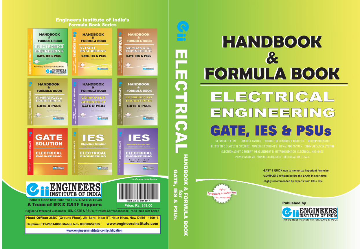
GATE, IES & PSUs
GATE, IES & PSUs
GATE, IES & PSUs

FORMULA BOOKfor
GATE, IES & PSU’s
ELECTRICALENGINEERING
Published by Engineers Institute of India

2016 By Engineers Institute of India
ALL RIGHTS RESERVED. No part of this work covered by the copyrightherein may be reproduced, transmitted, stored or used in any form or by anymeans graphic, electronic, or mechanical & chemical, including but notlimited to photocopying, recording, scanning, digitizing, taping, Webdistribution, information networks, or information storage and retrievalsystems.
Engineers Institute of India
28-B/7, Jia Sarai, Near IIT Hauz Khas New Delhi-110016
Tel: 011-26514888
For publication information, visit www.engineersinstitute.com/publication
ISBN: 978-93-5156-854-4
Price: Rs. 349/-

A WORD TO THE STUDENTS.GATE and Engineering Services Examinations are themost prestigious competitive examinations conductedfor graduate engineers. Over the past few years, theyhave become more competitive as more and morenumbers of aspirants are increasingly becominginterested in post graduate qualifications &government jobs for a secured and bright career.This Formula Book consists of well-illustrated concepts, importantformulae and diagrams, which will be highly beneficial at the last leg ofcandidate’s preparation.It includes all the subjects of Electrical Engineering, InstrumentationEngineering, which are required for all type of competitiveexaminations. Adequate emphasis has been laid down to all the majortopics in the form of Tips / Notes, which will be highly lucrative forobjective and short answer type questions.Proper strategy and revision is a mandatory requirement for clearingany competitive examination. This book covers short notes andformulae for Electronics & Communication Engineering. This book willhelp in quick revision before the GATE, IES & all other PSUs.With best wishes for future career
R. K. RajeshDirectorEngineers Institute of [email protected]
This book is dedicated to all
Electrical Engineers
Preparing for GATE, IES, SSC& Public sectorexaminations.

CONTENTS
1. NETWORK THEORY .............................................. 01-40
2. CONTROL SYSTEMS ............................................ 41-74
3. DIGITAL ELECTRONICS AND CIRCUITS ............. 75-118
4. MICROPROCESSORS .......................................... 119-136
5. ELECTRONIC DEVICES & CIRCUITS .................. 137-168
6. ANALOG ELECTRONICS .................................... 169-204
7. SIGNALS AND SYSTEMS ................................... 205-230
8. COMMUNICATION SYSTEMS ............................. 231-264
9. ELECTROMAGNETIC THEORY ........................... 265-286
10. MEASUREMENTS AND INSTRUMENTATION .... 287-308
11. ELECTRICAL MACHINES ................................... 309-392
12. POWER SYSTEMS ............................................. 393-448
13. POWER ELECTRONICS ..................................... 449-500
14. ELECTRICAL MATERIALS ................................ 501-514
Why IES?Indian engineering services (IES) constitute of engineers that work under thegovt. of India to manage a large segment of public sector economy whichconstitutes of Railroads, Public works, Power, Telecommunications, etc. IESremain the most sought-after careers for the engineering graduates in India. Acombined competitive examination is conducted by UPSC for recruitment tothe Indian Engineering Services. The exam constitutes of a written examfollowed by an interview for personality test.Why GATE?In the present competitive scenario, where there is mushrooming ofuniversities and engineering colleges, the only yardstick to measureand testthe calibre of engineering students is the GATE.The GATE AdvantageMany public sector undertakings such as BHEL, IOCL, NTPC, BPCL, HPCL, BARCand many more PSUs are using the GATE score for selecting candidates fortheir organizations. Students who qualify in GATE are entitled to a stipend ofRs 8,000 per month during their M.Tech. course. Better remuneration is beingoffered for students of M.Tech./ME as compared to those pursuing B.Tech/B.E.A good rank assures a good job. After joining M.Tech. at IITs and IISc, one canlook at a salary package ranging from Rs 7lakh to 30lakh per annum dependingupon specialization and performance. Clearing GATE is also an eligibility clausefor the award of JRF in CSIR Laboratories.Proper strategy and revision is a mandatory requirement for clearing anycompetitive examination. This book covers short notes and formulae forElectronics & Communication Engineering. This book will help in quickrevision before the GATE, IES & all other PSUs.
EE FORMULA BOOK 1. NETWORK THEORY [1]
Published by: ENGINEERS INSTITUTE OF INDIA. ALL RIGHTS RESERVED www.engineersinstitute.com
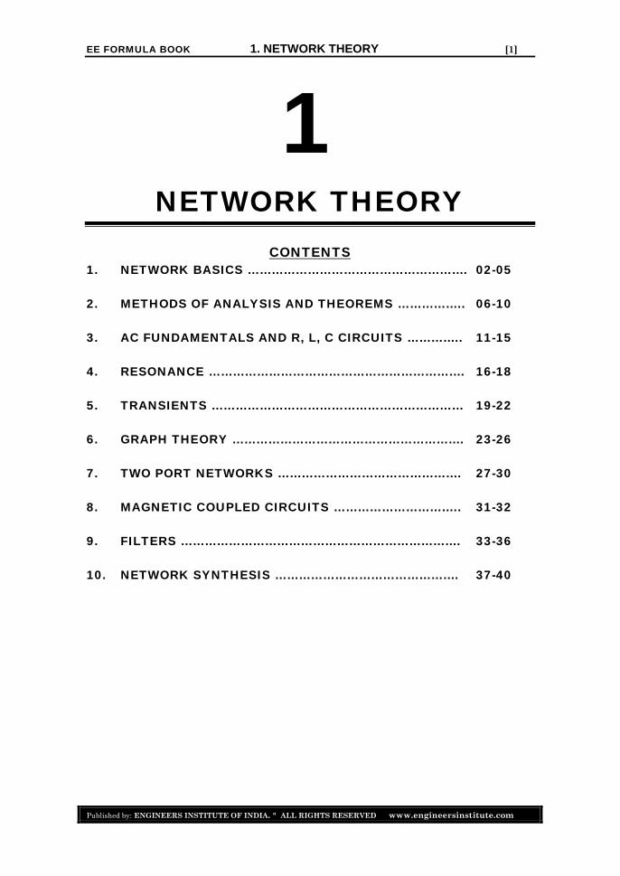
1NETWORK THEORY
CONTENTS1. NETWORK BASICS ………………………………………………. 02-05
2. METHODS OF ANALYSIS AND THEOREMS …………….. 06-10
3. AC FUNDAMENTALS AND R, L, C CIRCUITS ………….. 11-15
4. RESONANCE ………………………………………………………. 16-18
5. TRANSIENTS ……………………………………………………… 19-22
6. GRAPH THEORY …………………………………………………. 23-26
7. TWO PORT NETWORKS ………………………………………. 27-30
8. MAGNETIC COUPLED CIRCUITS ………………………….. 31-32
9. FILTERS ……………………………………………………………. 33-36
10. NETWORK SYNTHESIS ………………………………………. 37-40
EE FORMULA BOOK 1. NETWORK THEORY [2]
Published by: ENGINEERS INSTITUTE OF INDIA. ALL RIGHTS RESERVED www.engineersinstitute.com
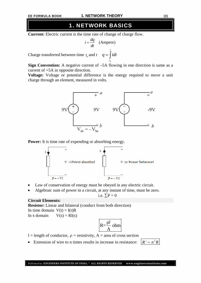
1. NETWORK BASICSCurrent: Electric current is the time rate of change of charge flow.
(Ampere)
Charge transferred between time and to
t
t
q idt Sign Convention: A negative current of –5A flowing in one direction is same as acurrent of +5A in opposite direction.Voltage: Voltage or potential difference is the energy required to move a unitcharge through an element, measured in volts.
Power: It is time rate of expending or absorbing energy.
Law of conservation of energy must be obeyed in any electric circuit. Algebraic sum of power in a circuit, at any instant of time, must be zero.
i.e. P = 0Circuit Elements:Resistor: Linear and bilateral (conduct from both direction)In time domain V(t) = I(t)RIn s domain V(s) = RI(s)
ρR= ohm
A
l
l = length of conductor, = resistivity, A = area of cross section
Extension of wire to n times results in increase in resistance: 2'R n R
dqi
dt
ot
EE FORMULA BOOK 1. NETWORK THEORY [3]
Published by: ENGINEERS INSTITUTE OF INDIA. ALL RIGHTS RESERVED www.engineersinstitute.com
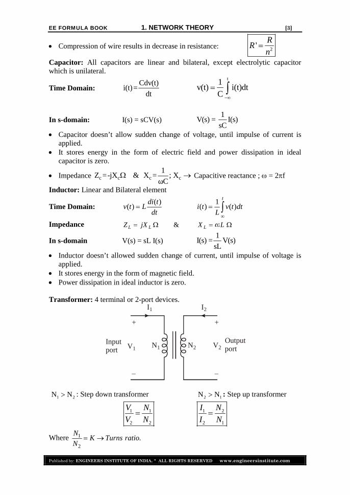
Compression of wire results in decrease in resistance: 2'R
Rn
Capacitor: All capacitors are linear and bilateral, except electrolytic capacitorwhich is unilateral.
Time Domain:Cdv(t)
i(t)=dt
t1v(t) i(t)dt
C
In s-domain: I(s) = sCV(s)1
V(s) = I(s)sC
Capacitor doesn’t allow sudden change of voltage, until impulse of current isapplied.
It stores energy in the form of electric field and power dissipation in idealcapacitor is zero.
Impedance c c c c1
Z =-jX & X = ; XωC
Capacitive reactance ; = 2f
Inductor: Linear and Bilateral element
Time Domain:( ) 1
( ) ( ) ( )t
di tv t L i t v t dt
dt L
Impedance &L L LZ jX X L
In s-domain V(s) = sL I(s)1
I(s) = V(s)sL
Inductor doesn’t allowed sudden change of current, until impulse of voltage isapplied.
It stores energy in the form of magnetic field. Power dissipation in ideal inductor is zero.
Transformer: 4 terminal or 2-port devices.
: Step down transformer : Step up transformer
1 1
2 2
V N
V N 1 2
2 1
I N
I N
Where 1
2
.N
K Turns ratioN
V1 N1 N2 V2
I2
+
–
Inputport
Outputport
I1
+
–
1 2N N 2 1N N
EE FORMULA BOOK 1. NETWORK THEORY [4]
Published by: ENGINEERS INSTITUTE OF INDIA. ALL RIGHTS RESERVED www.engineersinstitute.com
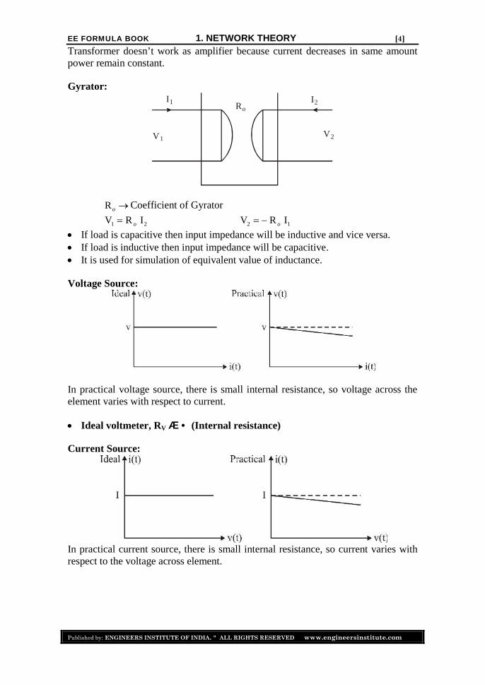
Transformer doesn’t work as amplifier because current decreases in same amountpower remain constant.
Gyrator:
Coefficient of Gyrator
If load is capacitive then input impedance will be inductive and vice versa. If load is inductive then input impedance will be capacitive. It is used for simulation of equivalent value of inductance.
Voltage Source:
In practical voltage source, there is small internal resistance, so voltage across theelement varies with respect to current.
Ideal voltmeter, RV (Internal resistance)
Current Source:
In practical current source, there is small internal resistance, so current varies withrespect to the voltage across element.
V1
Ro
V2
I2I1
Ro
1 2V R Io 2 1V R Io
EE FORMULA BOOK 1. NETWORK THEORY [5]
Published by: ENGINEERS INSTITUTE OF INDIA. ALL RIGHTS RESERVED www.engineersinstitute.com
Ideal Ammeter, Ra 0 (Internal resistance)
Dependent and Independent Source:Independent Source: Voltage or current source whose values doesn’t depend onany other parameters. E.g. Generator etc.
Dependent Source: Voltage or current source whose values depend upon otherparameters like current, voltage.The handling of independent and dependent voltage source is identical except.
(i) In Thevenin and Norton Theorem (ii) Superposition TheoremWhere, (i) All independent voltage sources are short circuited.
(ii) All independent current sources are open circuited.(iii) All dependent voltage and current sources are left as they are.
A network in which all network elements are physically separable is known aslumped network.
A network in which the circuit elements like resistance, inductance etc, are notphysically separate for analysis purpose, is called distributed network. E.g.Transmission line.
If an element is capable of delivering energy independently, then it is calledactive element.Example: Voltage source, Current source
If it is not capable of delivering energy, then it is passive element.Example: Resistor, Inductor, Capacitor
If voltage and current across an element are related to each other through aconstant coefficient then the element is called as linear element otherwise it iscalled as non-linear.
When elements characteristics are independent of direction of current thenelement is called bi-directional element otherwise it is called as unidirectional.Ex: R, L & C.
Diode is a unidirectional element. Voltage and current sources are also unidirectional elements. Every linear element should obey the bi-directional property but vice versa as is
not necessary. Internal resistance of voltage source is in series with the source. Internal
resistance of ideal voltage source is zero. Internal resistance of current source is in parellel with the source. Internal
resistance of ideal current source is infinite.

EE FORMULA BOOK 1. NETWORK THEORY [6]
Published by: ENGINEERS INSTITUTE OF INDIA. ALL RIGHTS RESERVED www.engineersinstitute.com
2. METHODS OF ANALYSIS AND THEOREMS(i) Kirchoff’s Points Law or Current Law (KCL): In any electrical network, thealgebric sum of the currents meeting at point (or junction) is zero.
Incoming current = Outgoing current
I1+I2 = I3+I4
It is based on conservation of charge.
(ii) Kirchoff’s Mesh Law or Voltage Law (KVL): The algebraic sum of productsof currents and resistance in each of conductor in any closed path in a network plusthe algebraic sum of emf in that path is zero.
i.e.It is based on conservation of energy.
Determination of Voltage Sign(a) Sign of Battery E.M.F.:
(b) Sign of IR Drop:
Resistors in Series: eq 1 2 3 nR = R + R + R +...... R
Resistors in Parallel:n
1.....+
R
Inductors in Series: eq 1 2 3 nL = L + L + L ....... L
Inductors in Parallel:eq 1 2 3 n
1 1 1 1 1= + + +......
L L L L L
Capacitors in Series:eq 1 2 3 n
1 1 1 1 1= + + +......
C C C C C
Capacitor in Parallel: eq 1 2 3 nC = C + C + C +...... C
IR emf 0
eq 1 2 3
1 1 1 1
R R R R
EE FORMULA BOOK 1. NETWORK THEORY [7]
Published by: ENGINEERS INSTITUTE OF INDIA. ALL RIGHTS RESERVED www.engineersinstitute.com
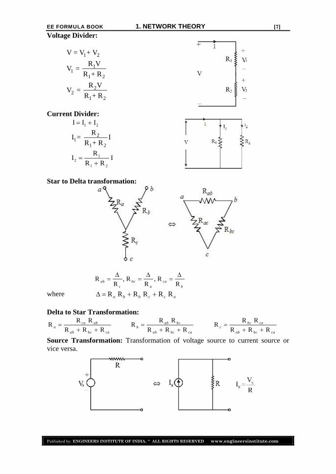
Voltage Divider:
1 2
11
1 2
22
1 2
V = V + V
R VV =
R + R
R VV =
R + R
Current Divider:
21
1 2
RI = I
R + R
Star to Delta transformation:
where
Delta to Star Transformation:
Source Transformation: Transformation of voltage source to current source orvice versa.
1 2I I I
12
1 2
RI I
R R
R , R , RR R Rab bc ca
c a b
R R R R R Ra b b c c a
R RR
R R Rca ab
aab bc ca
R RR
R R Rab bc
bab bc ca
EE FORMULA BOOK 1. NETWORK THEORY [7]
Published by: ENGINEERS INSTITUTE OF INDIA. ALL RIGHTS RESERVED www.engineersinstitute.com
Voltage Divider:
1 2
11
1 2
22
1 2
V = V + V
R VV =
R + R
R VV =
R + R
Current Divider:
21
1 2
RI = I
R + R
Star to Delta transformation:
where
Delta to Star Transformation:
Source Transformation: Transformation of voltage source to current source orvice versa.
R , R , RR R Rab bc ca
c a b
R R R R R Ra b b c c a
R RR
R R Rab bc
bab bc ca
R RR
R R Rbc ca
cab bc ca
EE FORMULA BOOK 1. NETWORK THEORY [7]
Published by: ENGINEERS INSTITUTE OF INDIA. ALL RIGHTS RESERVED www.engineersinstitute.com
Voltage Divider:
1 2
11
1 2
22
1 2
V = V + V
R VV =
R + R
R VV =
R + R
Current Divider:
21
1 2
RI = I
R + R
Star to Delta transformation:
where
Delta to Star Transformation:
Source Transformation: Transformation of voltage source to current source orvice versa.
EE FORMULA BOOK 1. NETWORK THEORY [8]
Published by: ENGINEERS INSTITUTE OF INDIA. ALL RIGHTS RESERVED www.engineersinstitute.com
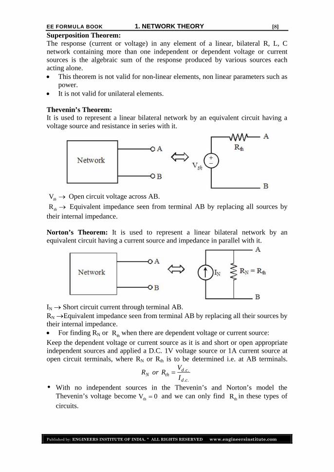
Superposition Theorem:The response (current or voltage) in any element of a linear, bilateral R, L, Cnetwork containing more than one independent or dependent voltage or currentsources is the algebraic sum of the response produced by various sources eachacting alone. This theorem is not valid for non-linear elements, non linear parameters such as
power. It is not valid for unilateral elements.
Thevenin’s Theorem:It is used to represent a linear bilateral network by an equivalent circuit having avoltage source and resistance in series with it.
Open circuit voltage across AB.
Equivalent impedance seen from terminal AB by replacing all sources bytheir internal impedance.
Norton’s Theorem: It is used to represent a linear bilateral network by anequivalent circuit having a current source and impedance in parallel with it.
IN Short circuit current through terminal AB.RNEquivalent impedance seen from terminal AB by replacing all their sources bytheir internal impedance. For finding RN or when there are dependent voltage or current source:Keep the dependent voltage or current source as it is and short or open appropriateindependent sources and applied a D.C. 1V voltage source or 1A current source atopen circuit terminals, where RN or Rth is to be determined i.e. at AB terminals.
. .
. .
d cN th
d c
VR or R
I
With no independent sources in the Thevenin’s and Norton’s model theThevenin’s voltage become and we can only find in these types ofcircuits.
Vth Rth
thR
thV 0 thR

EE FORMULA BOOK 2. CONTROL SYSTEMS [41]
Published by: ENGINEERS INSTITUTE OF INDIA. ALL RIGHTS RESERVED www.engineersinstitute.com
2CONTROL SYSTEMS
CONTENTS
1. BLOCK DIAGRAM ………………………………………………… 42-44
2. MATHEMATICAL MODELLING ………………………………. 45-46
3. TIME RESPONSE ANALYSIS ………………………………… 47-52
4. STABILITY …………………………………………………………. 53-55
5. ROOT LOCUS ……………………………………………………… 56-58
6. FREQUENCY DOMAIN ANALYSIS …………………………. 59-60
7. POLAR PLOTS …………………………………………………… 61-64
8. BODE PLOTS …………………………………………………….. 65-68
9. COMPENSATORS ……………………………………………….. 69-72
10. STATE SPACE ANALYSIS ……………………………………. 73-74
EE FORMULA BOOK 2. CONTROL SYSTEMS [42]
Published by: ENGINEERS INSTITUTE OF INDIA. ALL RIGHTS RESERVED www.engineersinstitute.com
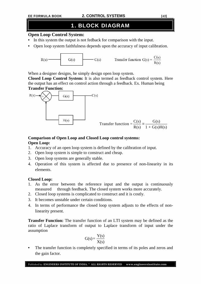
1. BLOCK DIAGRAMOpen Loop Control System: In this system the output is not fedback for comparison with the input.
Open loop system faithfulness depends upon the accuracy of input calibration.
When a designer designs, he simply design open loop system.Closed Loop Control System: It is also termed as feedback control system. Herethe output has an effect on control action through a feedback. Ex. Human beingTransfer Function:
C(s) G(s)Transfer function =
R(s) 1 + G(s)H(s)
Comparison of Open Loop and Closed Loop control systems:Open Loop:1. Accuracy of an open loop system is defined by the calibration of input.2. Open loop system is simple to construct and cheap.3. Open loop systems are generally stable.4. Operation of this system is affected due to presence of non-linearity in its
elements.
Closed Loop:1. As the error between the reference input and the output is continuously
measured through feedback. The closed system works more accurately.2. Closed loop systems is complicated to construct and it is costly.3. It becomes unstable under certain conditions.4. In terms of performance the closed loop system adjusts to the effects of non-
linearity present.
Transfer Function: The transfer function of an LTI system may be defined as theratio of Laplace transform of output to Laplace transform of input under theassumption
Y(s)G(s)=
X(s)
The transfer function is completely specified in terms of its poles and zeros andthe gain factor.

EE FORMULA BOOK 2. CONTROL SYSTEMS [43]
Published by: ENGINEERS INSTITUTE OF INDIA. ALL RIGHTS RESERVED www.engineersinstitute.com
The T.F. function of a system depends on its elements, assuming initialconditions as zero and is independent of the input function.
To find a gain of system through transfer function put s = 0
Example: G(s) = Gain =
If a step, ramp or parabolic response of T.F. is given, then we can find ImpulseResponse directly through differentiation of that T.F.
(Parabolic Response) = Ramp Response
(Ramp Response) = Step Response
(Step Response) = Impulse Response
Block Diagram Reduction:Rule Original Diagram Equivalent Diagram1. Combiningblocks in cascade
2. Moving asumming pointafter a block
3. Moving asumming pointahead of block
4. Moving a takeoff point after ablock
2
4
6 9
s
s s
4
9
d
dtd
dtd
dt
G1
X1G2
X G11X G G21 1 X1
G G21
X G G21 1
GX1
X1
X G1G
X1
X1
1/G
X G1

EE FORMULA BOOK 2. CONTROL SYSTEMS [44]
Published by: ENGINEERS INSTITUTE OF INDIA. ALL RIGHTS RESERVED www.engineersinstitute.com
5. Moving a takeoff point ahead ofa block
6. Eliminating afeedback loop
1 2(GX ± X )Signal Flow Graphs: It is a graphical representation of control system.
Signal Flow Graph of Block Diagram:
Mason’s Gain Formula: Transfer function =
Path gain of forward path
1 – [Sum of all individual loops] + [Sum of gain products of two non-touchingloops] – [Sum of gain products of 3 non-touching loops] + ………..
Value of obtained by removing all the loops touching forward path aswell as non-touching to each other
GX1 X G1
X G1
GX1
G
X G1
X G1
X1 G
1 GH
X2
k kp
kp thk
k thk
EE FORMULA BOOK 2. CONTROL SYSTEMS [45]
Published by: ENGINEERS INSTITUTE OF INDIA. ALL RIGHTS RESERVED www.engineersinstitute.com
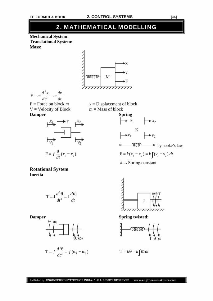
2. MATHEMATICAL MODELLINGMechanical System:Translational System:Mass:
F = Force on block m x = Displacement of blockV = Velocity of Block m = Mass of blockDamper Spring
by hooke’s law
Spring constant
Rotational SystemInertia
Damper Spring twisted:
2
2F
d x dvm m
dt dt
x2x1
v1 v2
K
1 2F ( )d
f x xdt
1 2 1 2F ( ) ( )k x x k v v dt k
2
1 22T ( )
df f
dt
T k k dt
2
2T J J
d d
dt dt

EE FORMULA BOOK 2. CONTROL SYSTEMS [46]
Published by: ENGINEERS INSTITUTE OF INDIA. ALL RIGHTS RESERVED www.engineersinstitute.com
Force Voltage and Force Current Analogy:
Voltage(Series RLC)
Current(Parallel RLC)
Force(Translational)
Torque(Rotational)
V I F Tq x
R f (Damper) f (Damper)
k k
L C M JI V Linear velocity Angular velocity
Conversion of Translational System to other Systems:
2
2
d x dxF M f kx
dt dt
Force–Current Analogy:
2
2
d 1 di C
dt R dt Ldv v 1
i C + + vdtdt R L
Force–Voltage Analogy:
2
2
d q dq qV L R
dt Cdt
di 1V L iR idt
dt C
1
R
1
C
1
L
EE FORMULA BOOK 2. CONTROL SYSTEMS [47]
Published by: ENGINEERS INSTITUTE OF INDIA. ALL RIGHTS RESERVED www.engineersinstitute.com
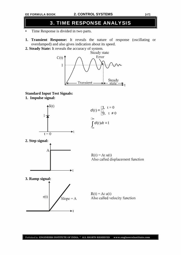
3. TIME RESPONSE ANALYSIS Time Response is divided in two parts.
1. Transient Response: It reveals the nature of response (oscillating oroverdamped) and also gives indication about its speed.
2. Steady State: It reveals the accuracy of system.
Standard Input Test Signals:1. Impulse signal:
1, t = 0( )
0, t 0
( ) 1
t
t dt
2. Step signal:
3. Ramp signal:

EE FORMULA BOOK 3. DIGITAL ELECTRONICS AND CIRCUITS [75]
Published by: ENGINEERS INSTITUTE OF INDIA. ALL RIGHTS RESERVED www.engineersinstitute.com
3DIGITAL ELECTRONICS
AND CIRCUITSCONTENTS
1. NUMBER SYSTEM & CODES …………………………………. 76-78
2. BINARY AIRTHMETIC ………………………………………….. 79-82
3. LOGIC GATES …………………………………………………….. 83-89
4. DIGITAL LOGIC CIRCUITS ……………………………………. 90-95
5. SEQUENTIAL CIRCUITS ………………………………………. 96-100
6. SHIFT REGISTERS ……………………………………………… 101-102
7. COUNTERS ………………………………………………………… 103-105
8. DIGITAL LOGIC FAMILY ……………………………………… 106-112
9. ADCs AND DACs ……………………………………………… 113-116
10. MEMORIES ……………………………………………………….. 117-118

EE FORMULA BOOK 3. DIGITAL ELECTRONICS AND CIRCUITS [76]
Published by: ENGINEERS INSTITUTE OF INDIA. ALL RIGHTS RESERVED www.engineersinstitute.com
1. NUMBER SYSTEM & CODESNumber System and Codes:
A number system with base ‘r’, contents ‘r’ different digits and they are from 0 tor – 1.Decimal to other codes conversions: To convert decimal number into other systemwith base ‘r’, divide integer part by r and multiply fractional part with r.
Other codes to Decimal Conversions:
Hexadecimal to Binary: Convert each Hexadecimal digit into 4 bit binary.
216
1111)(0101 1010(5 )
5AF
A F
Binary to Hexadecimal: Grouping of 4 bits into one hex digit.
Octal to Binary and Binary to Octal: Same procedure as discussed above but heregroup of 3 bits is made.
Codes:Binary coded decimal (BCD): In BCD code each decimal digit is represented with 4 bit binary format.
109 4 9
: (943) 1001 0100 0011BCD
Eg
It is also known as 8421 codeInvalid BCD codesTotal Number possibleValid BCD codes 10Invalid BCD codesThese are 1010, 1011, 1100, 1101, 1110, and 1111
Excess-3 code: (BCD + 0011) It can be derived from BCD by adding ‘3’ to each coded number. It is unweighted and self-complementing code.
2 1 0 1 2 10( . ) (A)rx x x y y 2 1 2
2 1 0 1 2A x r x r x y r y r
2 16(110101.11) 0011 0101.1100 (35.C)
42 16
16 10 6
EE FORMULA BOOK 3. DIGITAL ELECTRONICS AND CIRCUITS [77]
Published by: ENGINEERS INSTITUTE OF INDIA. ALL RIGHTS RESERVED www.engineersinstitute.com
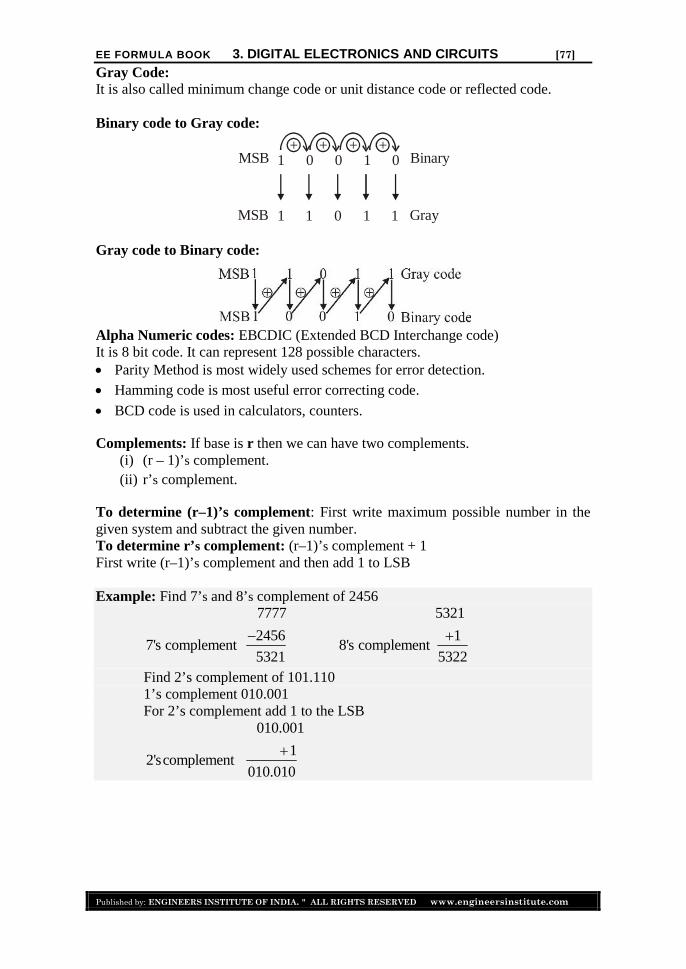
Gray Code:It is also called minimum change code or unit distance code or reflected code.
Binary code to Gray code:
Gray code to Binary code:
Alpha Numeric codes: EBCDIC (Extended BCD Interchange code)It is 8 bit code. It can represent 128 possible characters. Parity Method is most widely used schemes for error detection. Hamming code is most useful error correcting code.
BCD code is used in calculators, counters.
Complements: If base is r then we can have two complements.(i) (r – 1)’s complement.(ii) r’s complement.
To determine (r–1)’s complement: First write maximum possible number in thegiven system and subtract the given number.To determine r’s complement: (r–1)’s complement + 1First write (r–1)’s complement and then add 1 to LSB
Example: Find 7’s and 8’s complement of 24567777 5321
2456 17's complement 8's complement
5321 5322
Find 2’s complement of 101.1101’s complement 010.001For 2’s complement add 1 to the LSB
010.001
12'scomplement
010.010
+1 0 0 1 0
+ + +
1 1 0 1 1
MSB
MSB
Binary
Gray

EE FORMULA BOOK 3. DIGITAL ELECTRONICS AND CIRCUITS [78]
Published by: ENGINEERS INSTITUTE OF INDIA. ALL RIGHTS RESERVED www.engineersinstitute.com
Data Representation:
Unsigned Magritude: Range with n bit
Signed Magritude: Range with n bit
1’s complement: Range with n bit
2’ complement: With n bits Range
In any representation+ve numbers are represented similar to +ve number in sign magnitude.
10 to 2n 5 101 5 Not possible
1 1(2 1) to (2 1)n n 6 0110
sign bit sign bit
with 4 bits with 8 bits
6 1 110 1 0000110
1 1(2 1) to (2 1)n n 6 0110
sign bit 1's complement of 6
6 1 001
1 12 to (2 1)n n 6 0110
sign bit 2 's complement of 6
6 1 010

EE FORMULA BOOK 3. DIGITAL ELECTRONICS AND CIRCUITS [79]
Published by: ENGINEERS INSTITUTE OF INDIA. ALL RIGHTS RESERVED www.engineersinstitute.com
2. BINARY AIRTHMETICWhen both the numbers have same sign then we add only magnitude and use thesign of MSB.
1’ Complement Addition: When the numbers have different signs, keep onenumber as it is and take 1’s complement of the negative number and add them.If carry occurs:(a) add carry to LSB(b) sign of the result is sign of the complemented number.If carry does not occur:(a) take 1’s complement of the result(b) sign of the result is sign of the complemented number.
2’ Complement Addition: When the numbers have different signs, keep thepositive number as it is and take 2’s complement of the negative number and addthem.If carry occurs:(a) carry is discardedIf carry does not occur:(a) take 2’s complement of the result(b) sign of the result is sign of the complemented number
BCD Addition: Add the BCD numbers as regular true binary numbers.If the sum is 9(1001) or less, it is a valid BCD answer.If sum is greater than 9 or if there is carryout of MSB, it is an invalid BCD number.If it is invalid, add 6 (0110) to the result to make it valid. Any carry out of the MSBis added to the next more-significant BCD number.Repeat steps for each group of BCD bits
76 0111 0110
94 1001 0100Invalid BCD number
170 1 0000 1010
Add 6 (110) in the result, 1 7 0
1 0000 1010
0110 0110valid BCD number
1 0111 0000

EE FORMULA BOOK 3. DIGITAL ELECTRONICS AND CIRCUITS [80]
Published by: ENGINEERS INSTITUTE OF INDIA. ALL RIGHTS RESERVED www.engineersinstitute.com
Overflow concept: Overflow may occur when two same sign numbers are added.
Overflow condition : If x and y are the MSB’s of two numbers and z is resultantMSB after adding two numbers then overflow conditions is
BOOLEAN ALGEBRABasic Operations:
AND OR NOT
A.A=A A+A=A
A.0=0 A+0=A A=A
A.1=A A+1=1
A.A=0 A+A=1Boolean algebra Laws:Commutative Law: A + B = B + A and A.B = B.AAssociative Law: A + (B + C) = (A + B) + C = A + B + C
A.(B.C) = (A.B).C = A.B.C
Distributive Law: A.(B + C) = A.B + A.CTheorems: Distribution theorem: (A + B.C) = (A + B).(A + C)
A.(B + C) = A.B + A.CExample: A + AB = (A + A)(A + B) = (A + B)
A+AB (A+A)(A+B) A+B
Transposition Theorem: (A + B) . (A + C) = A + B.C
De Morgan’s Law:
1 2 n1 2 3 n
1 2 n1 2 3 n
A .A .A ......A =A +A +....+A
A +A +A .....+A =A .A .....A
Involution Theorem: A = AAbsorption Theorem: A + AB = ADual Expression: It will convert positive logic into negative and negative logic intopositive logic.Procedure:1. Change each OR sign by AND and vice-versa.2. Convert all 1s to 0s and all 0s to 1s.3. Keep variables as it is. If one time dual is as same as function then it is known as self dual expression.
1x y z x y z

EE FORMULA BOOK 3. DIGITAL ELECTRONICS AND CIRCUITS [81]
Published by: ENGINEERS INSTITUTE OF INDIA. ALL RIGHTS RESERVED www.engineersinstitute.com
Boolean Function Representation:Canonical Form: All terms contain each literal.
F(A, B, C) =
Standard form: All the terms do not have each literal.
Sum of Product (SOP) : In SOP form each product term is known as minterm. SOP forms are used to write logical expression so that the output becomes
logic ‘1’. Notation for SOP expression is f (A, B, C) = (3, 5, 6, 7)m
Product of Sum (POS):Example:
Each individual term in standard POS is called maxterm. POS forms are used to write logical expression so that the output becomes
logic‘0’.
Example: f (A, B, C) =
Y =
Implicant: Each individual minterm or group of minterms in canonical SOP iscalled implicant.Prime Implicant: It is a minterm, which are obtained by combining maximumpossible adjacent cells in k-map.Essential Prime Implicant: It is Prime Implicant in which one or more mintermsare unique.Example:1.
Possible K-map solutions:
PI:
EPI:
ABC ABC ABC
F(A, B, C) A BC ABC
Y ABC ABC ABC ABC
(A C) . (B E)
M(0,1, 2, 4)
(A B C) (A B C) (A B C) (A B C)
AB AB BC, AB AB AC
AB, AC, AB, BC
AB, AB

EE FORMULA BOOK 3. DIGITAL ELECTRONICS AND CIRCUITS [82]
Published by: ENGINEERS INSTITUTE OF INDIA. ALL RIGHTS RESERVED www.engineersinstitute.com
2.
A, B
A, B
PI :
EPI :
With n Variable
Maximum possible logic expressions
Minterms/Maxterms Self dual expressions
1 1
1 1
B C B C
A
B C B C
A 1 1
22n
2n122
n
EE FORMULA BOOK 6. ANALOG ELECTRONICS [169]
Published by: ENGINEERS INSTITUTE OF INDIA. ALL RIGHTS RESERVED www.engineersinstitute.com
6ANALOG ELECTRONICS
CONTENTS
1. VOLTAGE REGULATOR & RECTIFIERS …………………….. 170-171
2. BJT & TRANSISTOR BIASING …………………………………. 172-175
3. MULTISTAGE & POWER AMPLIFIERS ……………………… 176-178
4. SMALL SIGNAL ANALYSIS …......................................... 179-183
5. FEEDBACK AMPLIFIERS ………………………………………… 184-187
6. OSCILLATORS ………………………………………………………. 188-191
7. OPERATIONAL AMPLIFIERS …………………………………… 192-204
EE FORMULA BOOK 6. ANALOG ELECTRONICS [170]
Published by: ENGINEERS INSTITUTE OF INDIA. ALL RIGHTS RESERVED www.engineersinstitute.com
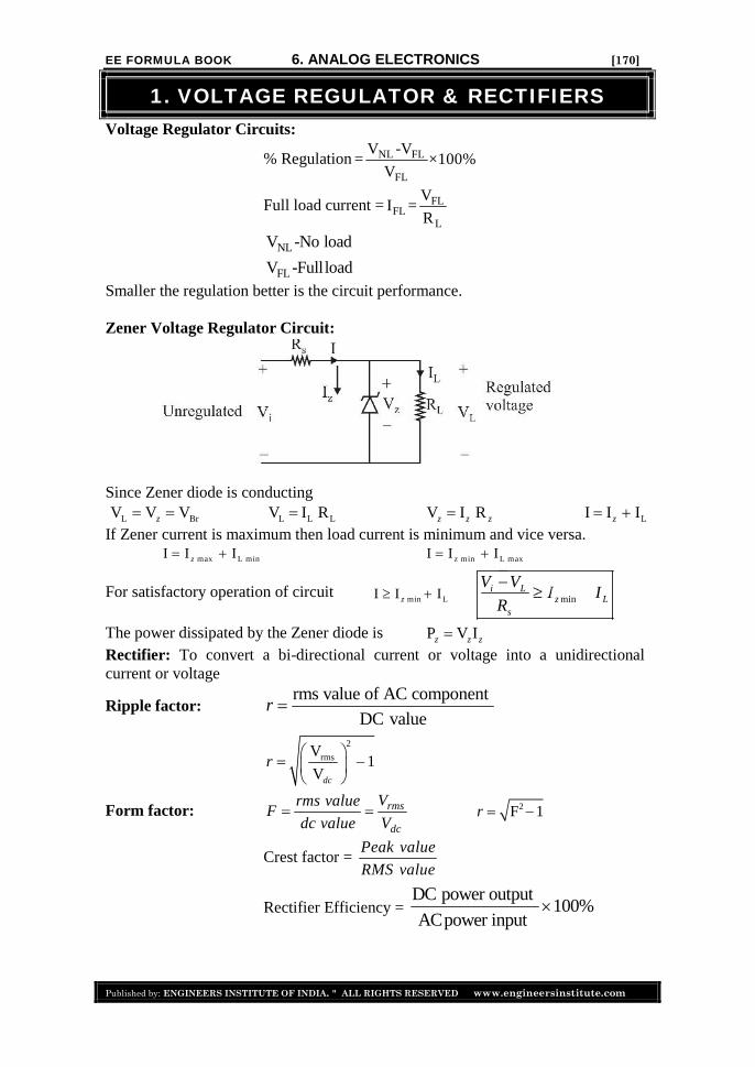
1. VOLTAGE REGULATOR & RECTIFIERSVoltage Regulator Circuits:
% Regulation NL FL
FL
V -V= ×100%
V
Full load current = FLFL
L
VI =
R
NL
FL
V -No load
V -FullloadSmaller the regulation better is the circuit performance.
Zener Voltage Regulator Circuit:
Since Zener diode is conducting
If Zener current is maximum then load current is minimum and vice versa.
For satisfactory operation of circuit mini L
z Ls
V VI I
R
The power dissipated by the Zener diode isRectifier: To convert a bi-directional current or voltage into a unidirectionalcurrent or voltage
Ripple factor:rms value of AC component
DC valuer
Form factor: rms
dc
Vrms valueF
dc value V
Crest factor =Peak value
RMS value
Rectifier Efficiency =DC power output
100%ACpower input
L BrV V Vz L L LV I R V I Rz z z LI I Iz
max L minI I Iz min L maxI I Iz
min LI I Iz
P V Iz z z
2
rmsV1
Vdc
r
2F 1r

EE FORMULA BOOK 6. ANALOG ELECTRONICS [171]
Published by: ENGINEERS INSTITUTE OF INDIA. ALL RIGHTS RESERVED www.engineersinstitute.com
TUF (Transformer utilization factor):
TUF =DC power output
ACrating of transformerHalf Wave Rectifier: Average value of current and voltage
RMS value of current and voltage:
Efficiency Ripper factor = 1.21Frequency of ripple voltage = f Form factor = 1.57Peak inverse voltage = TUF = 0.286
Full Wave Rectifier: Average value of current and voltage:
RMS value of current and voltage:
Efficiency Ripper factor = 0.48
From factor = 1.11 Crest factor =TUF = 0.692
Frequency of ripple voltage = 2f Peak inverse voltage =Bridge Rectifier: All the parameters are same as full wave rectifier exceptPeak inverse voltage = Transformer utilization factor = 0.812
Advantage of Bridge Rectifier:1. The current in both the primary and secondary of the transformer flows for entire
cycle.2. No center tapping is required in the transformer secondary. Hence it is a cheap
device.3. The current in the secondary winding of transformer is in opposite direction in
two half cycles. Hence net DC current flow is zero.4. As two diode currents are in series, in each of the cycle inverse voltage appear
across diode gets shared. Hence the circuit can be used for high voltageapplication.
dc
II ,m
dc
VV m
rms
II ,
2m rms
VV
2m
40.6%
Vm
dc dc
2I 2VI , Vm m
rms
VV ,
2m rms
II
2m
81.2%
2
2Vm
Vm

EE FORMULA BOOK 6. ANALOG ELECTRONICS [172]
Published by: ENGINEERS INSTITUTE OF INDIA. ALL RIGHTS RESERVED www.engineersinstitute.com
2. BJT & TRANSISTOR BIASING
General Equation of Transistor: In CE mode C B COI = βI + (1+ β)IIn CB mode
BE
T
O
V
VE CI I e
Typical values for = 0.2 (Ge Transistor)0.7 (Si Transistor)1.3 (GaAs Transistor)
(a) Condition to keep transistor in cut off: 0.7BEV V
(b) Condition for transistor under active region:
1. 0.7BEV V 2. C B EI I I 3.
(c) Transistor under saturation region:To find whether transistor is in active mode or saturation mode
0.7
0.2
BE
C B E
CEsat
V V
I I I
V V
I. If active > (saturation)
then transistor is in saturation and Qpoint is ( (saturation),0.2).
II. If (saturation) > (active)then transistor is in active region and Qpoint is ( (active), ).
C E COI I I
BEV
satB
II c
CI CI
CI
CI CI
CI CEV

EE FORMULA BOOK 6. ANALOG ELECTRONICS [173]
Published by: ENGINEERS INSTITUTE OF INDIA. ALL RIGHTS RESERVED www.engineersinstitute.com
Transistor DC Load Line and Q Point
DC load line is a straight line which joins or which joins saturation
and cutoff point. DC load line is the locus of all possible operating point at which it remains in
active region. Q point is called quiescent point or operating point and it is a function of IB, IC,
and VCC. For best performance of amplifier in the BJT the Q point must be located at the
center of D.C. load line.
Stability Factor:IC is a function of , , (T em perature dependent param eter )C O BEI V
Stability S =,BE
C
CO V
I
I
Smaller the values of S better will be thermal stability.
The general equation for stability factor S: 1
1 B
C
SI
I
Transistor Biasing Circuits and Their Stability:A. Fixed Bias Circuit (Base – Bias)
CC CEC
C
CC BEB
B
V VI
R
V VI
R
Stability 1S Fixed bias circuit is unstable.
max CCI and Vc
EE FORMULA BOOK 6. ANALOG ELECTRONICS [174]
Published by: ENGINEERS INSTITUTE OF INDIA. ALL RIGHTS RESERVED www.engineersinstitute.com
B. Collector to base bias circuits
( 1)CC BE
BC B
C B
V VI
R R
I I
Stability 1
1 C
C B
SR
R R
The circuit is having good thermal stability.
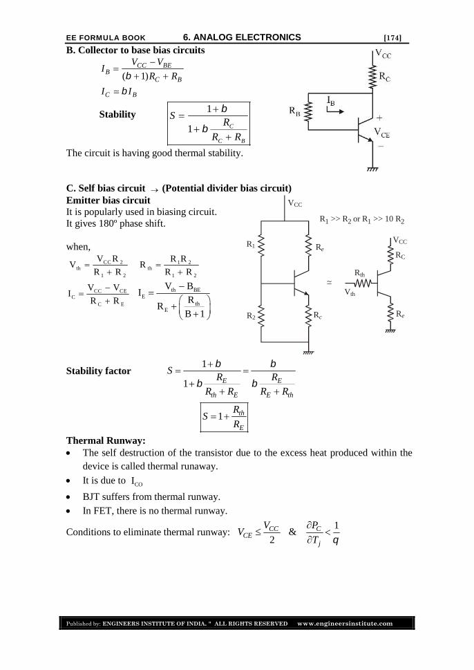
C. Self bias circuit (Potential divider bias circuit)Emitter bias circuitIt is popularly used in biasing circuit.It gives 180º phase shift.
when,
Stability factor1
1 E E
th E E th
SR R
R R R R
1 th
E
RS
R
Thermal Runway: The self destruction of the transistor due to the excess heat produced within the
device is called thermal runaway.
It is due to
BJT suffers from thermal runway. In FET, there is no thermal runway.
Conditions to eliminate thermal runway:1
&2
CC C
CEj
V PV
T
CC 2th
1 2
V RV
R R
1 2
th1 2
R RR
R R
CC CEC
C E
V VI
R R
th BE
Eth
E
V BI
RR
B 1
COI
Rth
Vth
VCC
RC
Re
R1
R2
VCC
Re
Rc
~–
R >>1 R or R >> 10 R2 1 2
EE FORMULA BOOK 6. ANALOG ELECTRONICS [175]
Published by: ENGINEERS INSTITUTE OF INDIA. ALL RIGHTS RESERVED www.engineersinstitute.com
Thermal resistance º C / watt or º / wattj A
D
T TK
P
Junction temperature (collector junction)
Ambient temperature
Power dissipated across collector junction
A transistor is thermally stable if C d
j j
dP dP
dT dT
C
j
dP
dTRate at which heat is released D
j
dP
dTRate at which heat is dissipated
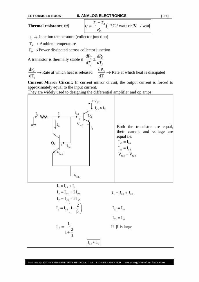
Current Mirror Circuit: In current mirror circuit, the output current is forced toapproximately equal to the input current.They are widely used to designing the differential amplifier and op amps.
Both the transistor are equal,their current and voltage areequal i.e.
1 3 4b bI I I
If is large
( )
T j
AT
DP
3 4I Ib b
3 4I Ic c
3 4V Vbc bc
2 4 1I I Ic
2 4 4I I 2Ic b
2 3 3I I 2 Ic b
2 3
2I I 1c
3 4I Ic c
3 4I Ib b
23
II
21
c
3 2I Ic
EE FORMULA BOOK 11. ELECTRICAL MACHINES [309]
Published by: ENGINEERS INSTITUTE OF INDIA. ALL RIGHTS RESERVED www.engineersinstitute.com
11ELECTICAL MACHINES
CONTENTS
1. TRANSFORMER…………………………………………………… 310-330
2. DC MACHINE ……………………………………………………… 331-346
3. SYNCHRONOUS MACHINES………………………………… 347-364
4. INDUCTION MACHINES ………………………………………. 365-381
5. FRACTIONAL KW MACHINES ………………………………. 382-392
EE FORMULA BOOK 11. ELECTRICAL MACHINES [310]
Published by: ENGINEERS INSTITUTE OF INDIA. ALL RIGHTS RESERVED www.engineersinstitute.com
1. TRANSFORMER
Definition: A transformer is a static device that transfers electrical energy from oneelectrical circuit to another electrical circuit through the medium of magnetic fieldand without the change of frequency.
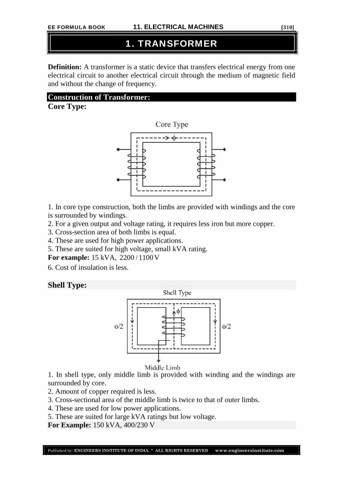
Construction of Transformer:Core Type:
1. In core type construction, both the limbs are provided with windings and the coreis surrounded by windings.2. For a given output and voltage rating, it requires less iron but more copper.3. Cross-section area of both limbs is equal.4. These are used for high power applications.5. These are suited for high voltage, small kVA rating.For example: 15 kVA, 2200 /1100V6. Cost of insulation is less.
Shell Type:
1. In shell type, only middle limb is provided with winding and the windings aresurrounded by core.2. Amount of copper required is less.3. Cross-sectional area of the middle limb is twice to that of outer limbs.4. These are used for low power applications.5. These are suited for large kVA ratings but low voltage.For Example: 150 kVA, 400/230 V

EE FORMULA BOOK 11. ELECTRICAL MACHINES [311]
Published by: ENGINEERS INSTITUTE OF INDIA. ALL RIGHTS RESERVED www.engineersinstitute.com
Principle of Transformer Action:
Figure (i)
A transformer works on the principle of electromagnetic induction betweentwo (or more) coupled circuits or coils. According to Faraday’s law ofelectromagnetic induction, an emf is induced in a coil if it links to changingflux.
The direction of induced emf is given by Lenz’s law which states that emf willbe induced in such a way that it opposes the cause which has produced it.
In transformer electrical energy is transferred due to mutual induction betweenprimary and secondary winding.
Emf equation of Transformer:Referring to figure (i), 1E = emf induced in the primary winding
2E = emf induced in the secondary winding
and 1 2N , N are the winding turns.
Let the flux is represented as, sinm t By Faraday’s law of electromagnetic induction,
Emf induced in primary winding, 1 1E Nd
dt
1 1E N ( sin )m
dt
dt 1 1E N cosm t
1 1E (E ) sin( 90º )m t rms value of emf induced in primary winding
11 rms
(E )(E )
2m
1 rms 1(E ) 2 N mf …(i)
Similarly, emf induced in secondary winding 2 2E Nd
dt
2 2E N sin( 90º )m t
22 rms
N(E )
2m

EE FORMULA BOOK 11. ELECTRICAL MACHINES [312]
Published by: ENGINEERS INSTITUTE OF INDIA. ALL RIGHTS RESERVED www.engineersinstitute.com
2 rms 2(E ) 2 N mf …(ii)
From equation (i) and (ii), 1 2
1 2
E E
N N
i.e., voltage per turns are equal in primary and secondary windings.From figure (i) we have, 1 1E V and 2 2E V
Hence, 1 1 1 2
2 2 2 1
V E N I
V E N Ia
Key Points:
1. Emf induced in the windings are2
radians ahead by the core flux.
2. Any change in the secondary current of the transformer causes a change inprimary current so that the flux remains constant.3. Infinite permeability of the core signifies that no magnetizing current is requiredfor establishment of flux.
Ideal Transformer:Properties(i) Resistance of the windings of transformer is zero.(ii) Magnetic leakage flux is zero.(iii) The permeability of the core of transformer is infinite.(iv) Efficiency is 100%.
Phasor diagram of an ideal transformer:
mmf balance equation: 1 1 2 2N I N I 0
2 21 2 2
1
N II I I
N a
2I = Secondary current referred to primary.

EE FORMULA BOOK 11. ELECTRICAL MACHINES [313]
Published by: ENGINEERS INSTITUTE OF INDIA. ALL RIGHTS RESERVED www.engineersinstitute.com
Phasor diagram of a Ideal Transformer (At Lagging pf load):
Note: As per IEEE, the turns ratio (a) = HV
LV
N
N
Where, NHV = Number of turns of HV windingNLV = Number of turns of LV winding
Practical Transformer ( ) In case of a practical transformer, Io current is required to produce flux in the coreand to compensate the core losses.
The mmf balance equation reads: 1 1 2 2 1N I N I N Io
21 2
1
NI I I
N o
1 2I I Io
Where Io is the exciting current/no load current.
Phasor Diagram of Practical Transformer on no load:
Here, Ic
core loss component of Io
I
= magnetizing component of Io
Note: Hysteresis angle ( ) shows us the lagging nature of w.r.t. Io

EE FORMULA BOOK 11. ELECTRICAL MACHINES [314]
Published by: ENGINEERS INSTITUTE OF INDIA. ALL RIGHTS RESERVED www.engineersinstitute.com
Circuit Representation of a practical Transformer
The KVL equations Read:
2 2 2 2 2 2E V I R I Xj
1 1 1 1 1 1V E I R I Xj
Figure: Transformer at Lagging Power Factor Load.
Equivalent circuit of Transformer:
Figure: Exact equivalent circuit referred to primary side.

EE FORMULA BOOK 11. ELECTRICAL MACHINES [315]
Published by: ENGINEERS INSTITUTE OF INDIA. ALL RIGHTS RESERVED www.engineersinstitute.com
Here, 2R ' represented the resistance of secondary winding referred to primary
Similarly, 22X ' and V '
represents reactance and voltage of secondary referred to
primary.
Let the no. of turns on primary be 1N and secondary be 2N
Hence, 12 2
2
NR ' R
N
12 2
2
NX ' X
N
12 2
2
NV ' V
N
22 2
1
NI ' I
N
Note:
No load current (I )o = 2% to 3% of full load current. This property of Io
leads
to further approximate circuits which are:
The voltage drop due to I0 in (R1+jX1) is so small that it can be neglected.
Note: Due to low value of Io
the magnetizing branch is sometimes totally ignored.
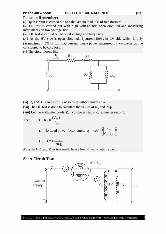
OC and SC tests on Transformer:Open Circuit Test:
EE FORMULA BOOK 11. ELECTRICAL MACHINES [316]
Published by: ENGINEERS INSTITUTE OF INDIA. ALL RIGHTS RESERVED www.engineersinstitute.com
Points to Remember:(i) Open circuit is carried out to calculate no load loss of transformer.(ii) OC test is carried out with high voltage side open circuited and measuringinstruments on low voltage side.(iii) OC test is carried out at rated voltage and frequency.(iv) As the HV side is open circuited, Io current flows in LV side which is only(at maximum) 5% of full load current, hence power measured by wattmeter can beconsidered to be core loss.(v) The circuit looks like
(vi) 1 1R and X can be easily neglected without much error.(vii) The OC test is done to calculate the values of RC and X(viii) Let the wattmeter reads OCP voltmeter reads OCV ammeter reads OCI
Then, (i)2
OCC
OC
(V )R
P
(ii) No Load power factor angle, 1 OC
OC OC
Pcos
V Io
(iii) CRX
tan o
Note: In OC test, o is too small, hence low Pf watt-meter is used.
Short Circuit Test:
EE FORMULA BOOK 12. POWER SYSTEMS [393]
Published by: ENGINEERS INSTITUTE OF INDIA. ALL RIGHTS RESERVED www.engineersinstitute.com
12POWER SYSTEMS
CONTENTS
1. FUNDAMENTAL OF ELECTRICAL POWER SYSTEM … 394-396
2. PER UNIT REPRESENTATION …………………………… 397-397
3. TRANSMISSION LINE ………………………………………. 398-405
4. TRAVELLING WAVES ………………………………………. 406-406
5. CABLE & INSULATOR ……………………………………… 407-409
6. ADMITTANCE & IMPEDENCE MODEL OF NETWORK 410-413
7. LOAD FLOW STUDIES ………………………………………. 414-416
8. ECONOMIC LOAD DISPACTCH …………………………. 417-418
9. FAULT ANALYSIS …………………………………………… 419-426
10. POWER SYSTEM STABILITY ……………………………. 427-430
11. SAG AND TENSION ………………………………………….. 431-432
12. CORONA …………………………………………………………. 433-438
13. POWER SYSTEM PROTECTION …………………………. 439-442
14. CIRCUIT BREAKER ………………………………………….. 443-444
15. HVDC-HIGH VOLTAGE DC TRANSMISSION …………. 445-448
EE FORMULA BOOK 12. POWER SYSTEMS [394]
Published by: ENGINEERS INSTITUTE OF INDIA. ALL RIGHTS RESERVED www.engineersinstitute.com
1. FUNDAMENTAL OF ELECTRICAL POWER SYSTEM
Work done = F.d cos Where F= force applied , d = displacement, = angle between F & dEnergy: It is capacity to do the work.
Unit : watt second 1w s 1Joule 1N m Newton meters
Electrical energy : It is energy that is in charged particles in an electric field.Electrical energy generally expressed in kilo watt hours (kwh)
61 kwh 3.6 10 J
Kinetic energy (KE): 21
2mv (Jules)
Potential Energy (PE): Mgh (Jules)Thermal Energy: Internal energy present in system by virtue of its temperature.
Unit : Calories 1 Cal 4.186 JPower: it is time rate of change of energy
dw duP
dt dt u = work, w = energy
Unit : Watt 1 Watt 1 J / sNote: Electric motor ratings are expressed in horse power (hp)1hp = 745.7 W and also 1 metric horse power = 735 Watt.
Electric parameter:Let 2 sinv V t
2 sin( )i I t where v = instantaneous value voltage
i = instantaneous value currentV = rms value of voltageI = rms value of voltage
In Phasor representation0 ,v V i I
S = P+jQ = VI cos + jVI sin = VI* (for this relation Q will be positive forlagging VAR)Where S = complex power or apparent power
P = Active powerQ = Reactive power
EE FORMULA BOOK 12. POWER SYSTEMS [395]
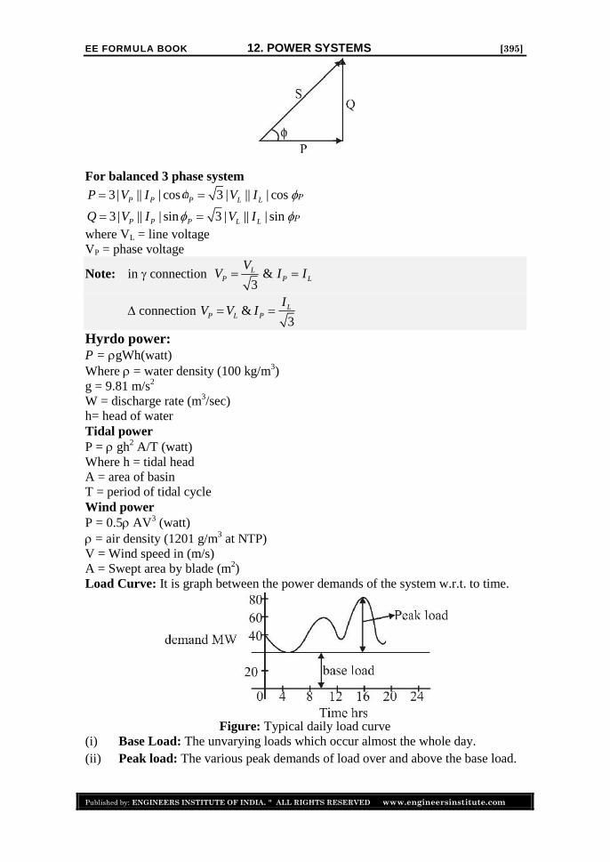
Published by: ENGINEERS INSTITUTE OF INDIA. ALL RIGHTS RESERVED www.engineersinstitute.com
For balanced 3 phase system3 | || | cos 3 | || | cosP P P L LP V I V I P3 | || | sin 3 | || | sinP P P L LQ V I V I P
where VL = line voltageVP = phase voltage
Note: in connection &3L
P P L
VV I I
connection &3L
P L P
IV V I
Hyrdo power:P = gWh(watt)Where = water density (100 kg/m3)g = 9.81 m/s2
W = discharge rate (m3/sec)h= head of waterTidal powerP = gh2 A/T (watt)Where h = tidal headA = area of basinT = period of tidal cycleWind powerP = 0.5 AV3 (watt) = air density (1201 g/m3 at NTP)V = Wind speed in (m/s)A = Swept area by blade (m2)Load Curve: It is graph between the power demands of the system w.r.t. to time.
Figure: Typical daily load curve(i) Base Load: The unvarying loads which occur almost the whole day.(ii) Peak load: The various peak demands of load over and above the base load.

EE FORMULA BOOK 12. POWER SYSTEMS [396]
Published by: ENGINEERS INSTITUTE OF INDIA. ALL RIGHTS RESERVED www.engineersinstitute.com
Designationcapacity
Capital cost Fuel cost Typicalannual loadfactor
Type of plant
Base load High Low 65-75 Nuclear,thermal
Peak load Low High 5-10 Gas based,small hydro,pump storage
Operational factors :
1. Demand Factor =Maximum demand
Connected load
2.energy consumed is a given period
Average loadHours in that time period
3.Average demand
Load factorMaximum load
4.sum of individual max demands
Diversity factorMaximum demand on power station
5.Average demand
Plant Capacity factorInstalled capcity
6. Reserve Capacity = Plant capacity - max. demand
7.Actual energy produced
Plant use factorPlant capacity hours (the plant has been in operation)
Note:1. Load factor can be defined for a period such daily load factor, monthly load
factor, annual load factor etc.2. Practically load factor is less than 1.3. Practically diversity factor is greater than 1.4. Both factors should be high for economical use.

EE FORMULA BOOK 12. POWER SYSTEMS [397]
Published by: ENGINEERS INSTITUTE OF INDIA. ALL RIGHTS RESERVED www.engineersinstitute.com
2. PER UNIT REPRESENTATION
the actual valuein any unitPer unit value
the base value in same unit
For single phaseLet Base volt amperes = (VA)B
Base voltage = VB V
Base current( )B
B
VAA
V
Base Impedance =2
( )B B
BB B
V VZ ohms
I VA
2
( ) ( )( ) B
B B
Z ohms VAZZ pu
Z V
where Z(ohms) = actual ImpedancePp.u = Vp.u Ip.u cos
For 3 phaseThere phase base mega votamperes = (MVA)B
Line to line base kilovolts = (KV)B
Base current1000 ( )
3 ( )B
B
B
MVAI
KV
Base Impedance2( )
( )B
BB
KVZ ohms
MVA
Pp.u (3-)= Vp.u Ip.u cos
Change of base2
, ,
2, ,
( ) ( )( ) ( )
( ) ( )B new B old
new oldB old B new
MVA KVZ Pu Z Pu
MVA KV
( )pu newZ New base value of impedence
( )pu oldZ Old base value of impedence
EE FORMULA BOOK 12. POWER SYSTEMS [398]
Published by: ENGINEERS INSTITUTE OF INDIA. ALL RIGHTS RESERVED www.engineersinstitute.com
3. TRANSMISSION LINE
Transmission line parameterResistanceThe effective Ac resistance
2
( )( )ac
average power loss in conductor wattsR ohm
I
Where I = Rms current (amp) in conductor
DC resistance ( )DC
lR ohms
A
= resistivity of the conductor, ohm-ml = length, mA = Cross-sectional area, m2
Note:(i) ac dcR R if current distribution in conductor is uniform.
(ii) At 50Hz acR is 4% to 8% more than dcR .
(iii) Skin effect & Proximity effect both are proportional to frequency.(iv) The temperature dependence of resistance
2 1 2 11 ( )R R T T
where 2 1&R R are the resistance at temperature T1 and T2 respectively
= temp. Coefficient of resistance
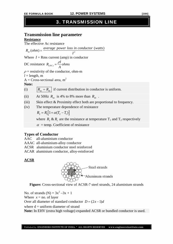
Types of ConductorAAC all-aluminium conductorAAAC all-aluminium-alloy conductorACSR aluminium conductor steel reinforcedACAR aluminium conductor, alloy-reinforced
ACSR
Figure: Cross-sectional view of ACSR-7 steel strands, 24 aluminium strands
No. of strands (N) = 3x2 –3x + 1Where x = no. of layerOver all diameter of standard conductor (2 1)D x d where d = uniform diameter of strandNote: In EHV (extra high voltage) expanded ACSR or bundled conductor is used.

EE FORMULA BOOK 12. POWER SYSTEMS [399]
Published by: ENGINEERS INSTITUTE OF INDIA. ALL RIGHTS RESERVED www.engineersinstitute.com
InductanceSingle phase two wire line
74 10 ln /'
DL H m
r
Where D is distance between the centres of the conductors1/4' 0.7788r re r Geometric mean radius
r = radius of conductorsComposite Conductor
Figure: Single-phase line consisting of two composite conductors
7
7
2 10 ln /
2 10 ln /
mA
sA
mB
sB
DL H m
D
DL H m
D
71/24 10 ln /
( )m
A BsA sB
DL L L H m
D D
Where mD mutual geometric mean distance1/ '
'
1 1
m nn m
iji j
D
sAD self geometric mean distance of A21/
1 1
nn n
iji j
D
Note: Composite inductance calculation is general formula. It can be extended forbundled conductor also.
Three phase three wire line inductance
EE FORMULA BOOK 12. POWER SYSTEMS [400]
Published by: ENGINEERS INSTITUTE OF INDIA. ALL RIGHTS RESERVED www.engineersinstitute.com
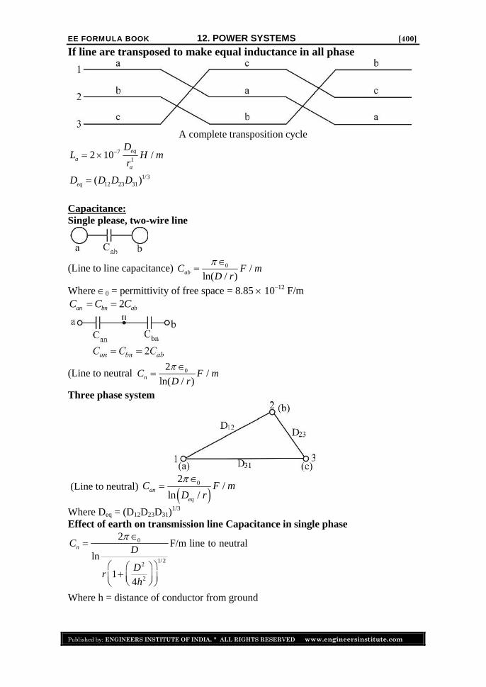
If line are transposed to make equal inductance in all phase
A complete transposition cycle
71
1/312 23 31
2 10 /
( )
eqa
a
eq
DL H m
r
D D D D
Capacitance:Single please, two-wire line
(Line to line capacitance) 0 /ln( / )abC F m
D r
Where 0 = permittivity of free space = 8.85 10–12 F/m2an bn abC C C
(Line to neutral 02/
ln( / )nC F mD r
Three phase system
(Line to neutral) 02
/ln /
an
eq
C F mD r
Where Deq = (D12D23D31)1/3
Effect of earth on transmission line Capacitance in single phase0
1/22
2
2F/m line to neutral
ln
14
nCD
Dr
h
Where h = distance of conductor from ground