gate-all-around si nanowire transistors (snwts) for ... · iedm, 2008 leti top-down process for...
TRANSCRIPT

1
Gate-All-Around Si NanowireTransistors (SNWTs) for
Extreme Scaling: Fabrication, Characterization and Analysis
Ru HuangPeking University (PKU)
Beijing 100871, China

2
Outline• Introduction• Fabrication and integration• Recent advances in understanding SNWTs
– Parasitic effects– Self-heating effects– Variability
• Recent nanowire circuit demonstrations• Summary

3
Introduction - 1/5

4
Introduction - 2/5We are entering the multi-gate era!
• Intel’s 22nm is Tri-gate transistor
• What’s next?Source: M. Bohr and K. Mistry, http://www.intel.com

5
Introduction - 3/5Next: Gate-all-around Nanowire Transistor
FinChannels
ExtremeScaling Nanowire
Channels
FinFET/Tri-gate Gate-all-around
“the ideal transistor” best gate controllability relax the strict scaling
requirement of tOX and Tsi
SourceExt.
DrainExt.
Gate All
Around
Number of Gates2 3 3+ 4+
Upper Limitof TSi / LG
Scalability
1/2
2/3
2
1 Double-gate
FinFETTri-gateFinFET
-gate-gate cylindricalrectangular
Gate-all-around
4Number of Gates
2 3 3+ 4+
Upper Limitof TSi / LG
Scalability
1/2
2/3
2
1 Double-gate
FinFETTri-gateFinFET
-gate-gate cylindricalrectangular
Gate-all-around
4

6
Strongly-confined quasi-1D structure
Introduction - 4/5How to fabricate this device?
Did we know all about this kind of device?• We already have the scaling theory for Tri-gate and GAA• But, one cannot simply scale GAA properties to get
correct understanding of Si nanowire transistor
Carriertransport?
Carriertransport?
Self-heating?
Self-heating?
Noise?Noise?
Reliability?Reliability? Source Drain
3D System
3D System
Quasi-1D System
Drain Ext.
Gate
Source Ext.
Source Drain
3D System
3D System
Quasi-1D System
Drain Ext.
Gate
Source Ext.
Variability?Variability?
Parasitics?Parasitics?
fundamentallydifferent !
Fabrication?Fabrication?

7
Transport?Transport?
Self-heating?
Reliability?Reliability?
Variability?Variability?
Parasitics?Parasitics?
Noise?Noise?
GAA SNWTs
R. Wang, et al., IEDM 2008R. Wang, et al, T-ED 2008
J. Zhuge, et al., T-ED 2008J. Zou, et al, T-ED 2011
J. Zhuge, et al., EDL 2008J. Zhuge, et al., APL 2009C. Liu, et al, IEDM 2011J. Zhuge,et al., IEDM 2009
R. Wang, et al, IEDM 2010C. Liu et al, IEDM 2011T. Yu, et al., T-ED 2010R. Wang, et al, T-ED 2011.
R. Wang, et al., IEDM 2008J. Zhuge, et al., T-Nano 2008X. Huang, et al., ISQED 2012
R. Wang, et al., IEDM 2007L. Zhang, et al., IEDM 2008L. Zhang, et al., VLSI 2009C. Liu, et al., T-ED 2010C. Liu, et al., IEDM 2011
• clarify the related physics• find the challenges for optimization• new characterizing techniques• ……
Introduction - 5/5
Fabrication?Fabrication?Y. Tian, et al., IEDM 2007
Fabricate this device from top-down approach Evaluate the key device characteristics for circuit
applications with confined quasi-1D structure

8
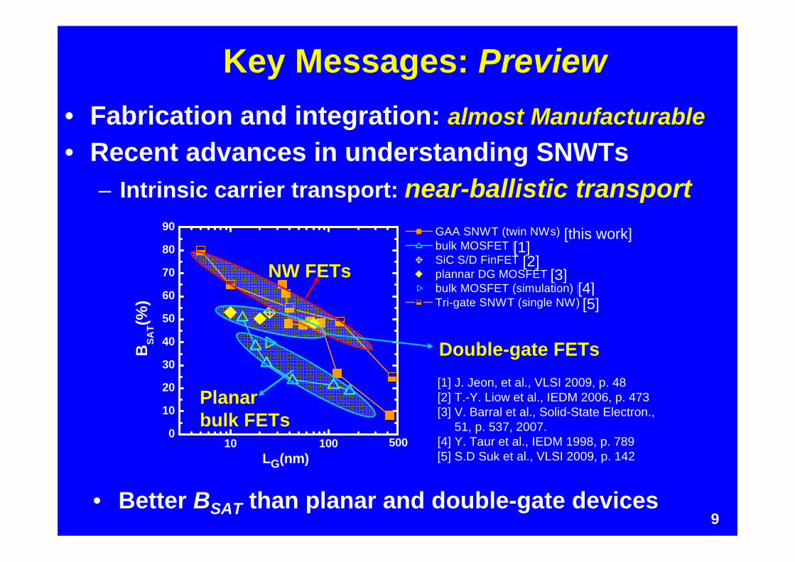
Key Messages: Preview• Fabrication and integration: almost Manufacturable• Recent advances in understanding SNWTs
– Intrinsic carrier transport: near-ballistic transport
9
Key Messages: Preview• Fabrication and integration: almost Manufacturable• Recent advances in understanding SNWTs
– Intrinsic carrier transport: near-ballistic transport
10 1000
10
20
30
40
50
60
70
80
90 GAA SNWT (twin NWs) [x] bulk MOSFET [x] SiC S/D FinFET [x] plannar DG MOSFET [x] bulk MOSFET (simulation) [x] Tri-gate SNWT (single NW) [x]
BSA
T(%)
LG(nm)500
NW FETs
Double-gate FETs
Planarbulk FETs
[this work]
[2][3]
[4][5]
[1]
[1] J. Jeon, et al., VLSI 2009, p. 48[2] T.-Y. Liow et al., IEDM 2006, p. 473 [3] V. Barral et al., Solid-State Electron.,
51, p. 537, 2007. [4] Y. Taur et al., IEDM 1998, p. 789[5] S.D Suk et al., VLSI 2009, p. 142
• Better BSAT than planar and double-gate devices

10
Key Messages: Preview• Fabrication and integration: almost Manufacturable• Recent advances in understanding SNWTs
– Intrinsic carrier transport: near-ballistic transport– Low-frequency noise: slightly degraded and fluctuated– Parasitic effects (R and C): should be optimized– Self-heating effects: observable when dNW<14nm– Variability: holds the record low (static) variations– Reliability: HCI is OK, but NBTI needs more studies
• Recent nanowire circuit demonstrations: On the way– SRAM, ring oscillator, current mirror…
• Other benefits for 3D integration, MtM applications…• Summary: We are facing a great opportunity!

11
Key Messages: Preview• Fabrication and integration: almost Manufacturable• Recent advances in understanding SNWTs
– Intrinsic carrier transport: near-ballistic transport– Low-frequency noise: slightly degraded and fluctuated– Parasitic effects (R and C): should be optimized– Self-heating effects: observable when dNW<14nm– Variability: holds the record low (static) variations– Reliability: HCI is OK, but NBTI needs more studies
• Recent nanowire circuit demonstrations: On the way– SRAM, ring oscillator, current mirror…
• Other benefits for 3D integration, MtM applications…• Summary: We are facing a great opportunity!

12
Outline• Introduction• Fabrication and integration
– based on bulk (our focus)– based on SOI– with stacked NW channel
• Recent advances in understanding SNWTs– Parasitic effects– Self-heating effects– Variability
• Recent nanowire circuit demonstrations• Summary

13
Purdue
TiN
SiO2
SiSamsung
SNWGox SNWGox
Poly-Gate
BOX
SNWGox SNWGox
Poly-Gate
BOX
NUS
Poly Silicon
Oxide10 nm Silicon Nanowire
Poly Silicon
Oxide10 nm Silicon Nanowire
OxideOxide
10 nm Silicon Nanowire10 nm Silicon Nanowire
OxideOxide
10 nm Silicon Nanowire10 nm Silicon Nanowire
PKU
NUS
IBMLETI
C. Dupré et al., IEDM, 2008LETI
Top-down process for SNWTs
IEDM, 2006NUS
IEDM, 2005Samsung
IEDM, 2007PKU
• Key points– NW formation– NW releasing or suspending
Sato S, et al., SSE, 2010, TIT
S. Bangsaruntipet al., IEDM, 2009IBM
TIT

14
Bulk SNWTs - Samsung method
S.D.Suk et al., IEDM, 2005
HM Trimming for NW definitionSiGe/Si stack epi for releasing
HM trimming
diameter = 10nmtOX=3.5nmTiN metal-gate

15
Self-aligned bulk SNWTs by epi-free compatible process
based on bulk substrate NW originally defined by e-beam, thinning and cylinder channel shaping by self-limiting oxidation and annealing NW released by isotropic etch with HM
Y. Tian et al., IEDM, 2007, PKU
16
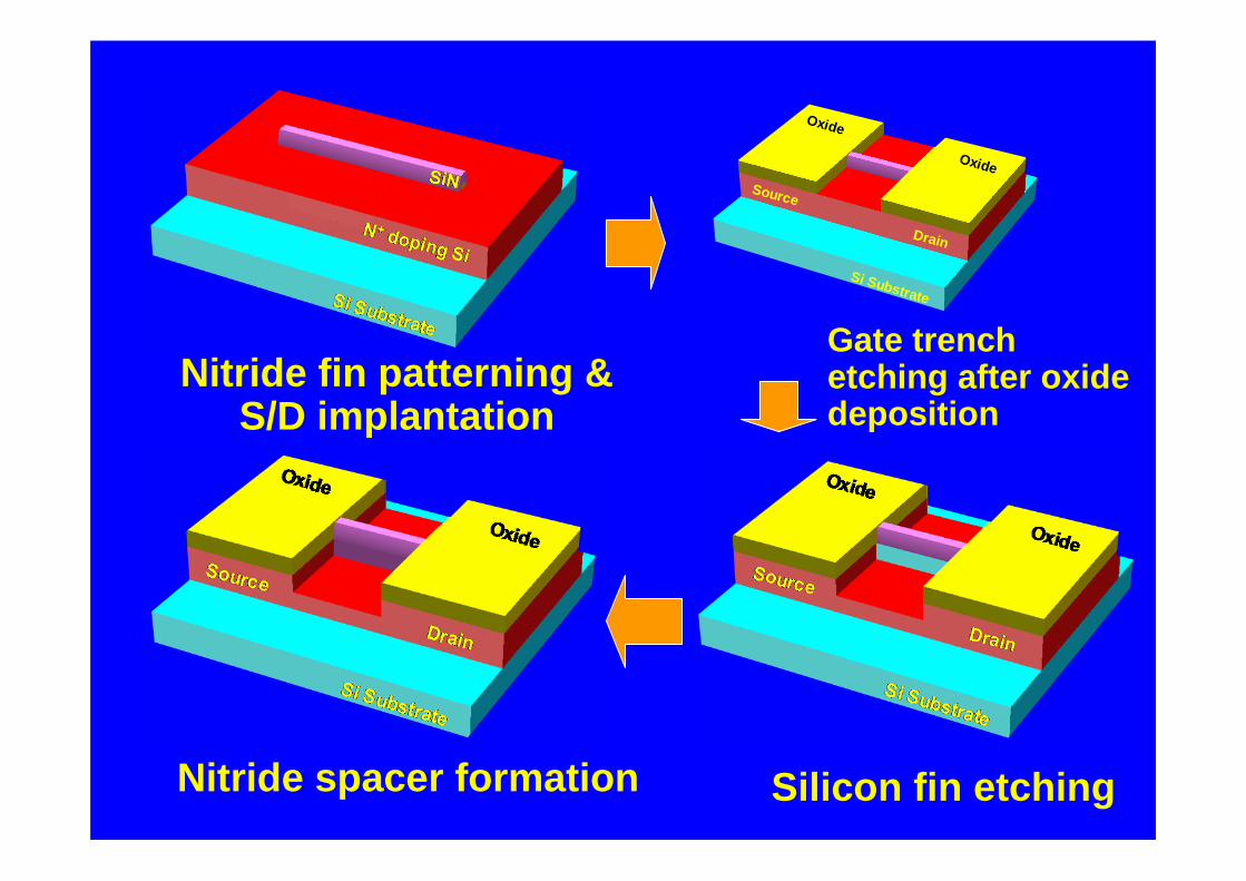
Nitride fin patterning & S/D implantation
Oxide
Si Substrate
Source
Oxide
Drain
Oxide
Si Substrate
Source
Oxide
Drain
Silicon fin etchingNitride spacer formation
Gate trench etching after oxide deposition

17
Silicon etching surrounding fin channel
Si etching under channel
BPT(bottom parasitic transistor) Stopper layerHard mask removal

18
Cylindrical shaping Gate oxidation &Poly-Si gate formation
• diameter = 10nm• tOX=5nm• Poly gate
19
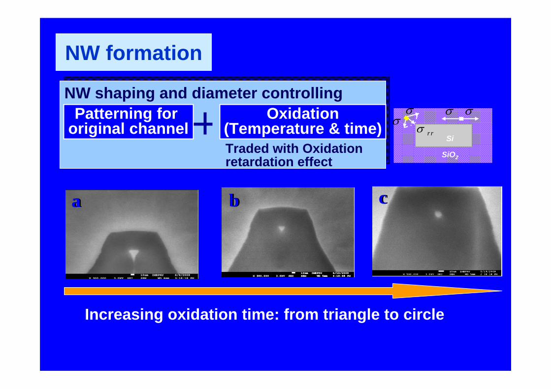
aa bb cc
Increasing oxidation time: from triangle to circle
SiO2
rrSi
Oxidation(Temperature & time)
NW shaping and diameter controllingPatterning for
original channelTraded with Oxidation retardation effect
NW formation

20
Experimental results of NWFETs
Single wire
Multiple wireY. Tian et al., IEDM, 2007, PKU
SourceSource
DrainDrain
Damascene Damascene Gate GrooveGate Groove

21
Current mirror (CM) based on SNWTs
2T CM
cascade CM
Single NW
R.Huang et al.,T-ED,2011,PKU adjust current ratio with NW number
Multi NW

22
OVC(%)=100(IOUT/IOUT)/VOUT
0 2 4 6 8 10
0
10
20
symbols: results
VOUT=0.3~1.2V
lines: linear fittingcurrent ratio (IOUT:IIN) Inversion
I O
UT (
A)
IIN(A)
1:2 1:1 4:1
0.0 0.2 0.4 0.6 0.8 1.0 1.20
2
4
6
8
output voltage swing
Inversion IIN=8A
IIN=6A
IIN=4A
IIN=2A
symbols: 2-T NWCMlines: 2-T PCM
I OU
T (A
)
VOUT (A)
OVC NW CM Planar CM2T ~0.2% ~5.7%
cascade ~0.05% ~1%
Testing results
23
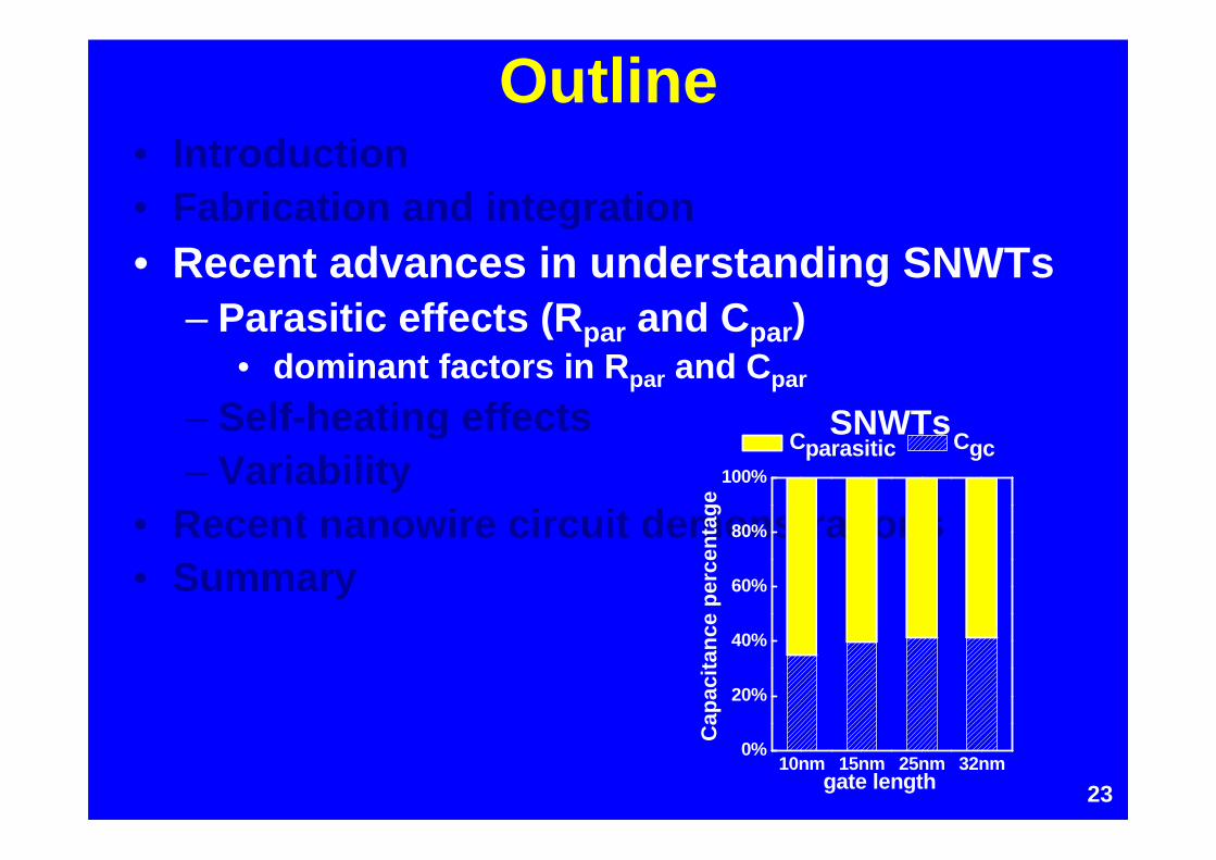
Outline• Introduction• Fabrication and integration• Recent advances in understanding SNWTs
– Parasitic effects (Rpar and Cpar)• dominant factors in Rpar and Cpar
– Self-heating effects– Variability
• Recent nanowire circuit demonstrations• Summary
10nm 15nm 25nm 32nm0%
20%
40%
60%
80%
100%
gate length
Cap
acita
nce
perc
enta
ge
Cparasitic CgcSNWTs

24
Parasitic R and C in GAA SNWTs• SNWT is worse
than planar devices and FinFETs– larger and
dominant SDE series resistances
– larger outer fringing capacitances
RsdRext
Rsd

25
Cparasitic = Cof + Cif + Cov + Cside
Parasitic capacitances in SNWTs
Cof = Cof_gsd + Cof_gex
• A predictive model for parasitic C in SNWTs has been developed*
*Jibin Zou et al., T-ED, vol. 58, no. 10, Oct. 2011,PKU

26
Impacts of parasitic C -1/2
10nm 15nm 25nm 32nm0%
5%
10%
15%
20%
25%
30%
Para
sitic
cap
acita
nce
perc
enta
ge
gate length
Cif
Cside
Cov
Cof
J. Zhuge et al., T-ED 2008, p. 2142; PKUJibin Zou et al., IEEE T-ED, vol. 58, no. 10, Oct. 2011.PKU
10nm 15nm 25nm 32nm0%
20%
40%
60%
80%
100%
Out
er fr
inge
cap
acita
nce
gate length
Cof_gsd Cof_gex
• Outer fringe capacitance Cof is dominant– Cof_gsd is the main contributor
Cof_gsd
CifSource Extension
Gate
Cov
Source
Cof_gex
Lex
Hg
dw
Cside

27
Key messages for design optimization of parasitics in SNWTs
• multi-wire structure is needed– with merged SDE structure
• gate height need to be reduced• Optimizations in SDE regions
– different from DG FinFETs• FinFETs: underlap is
better • SNWTs: overlap is better due to better gate control
capability in SNWTs can effectively reduce Rext
but with smaller impact on Cparastic
J. Zhuge et al., T-ED 2008, p. 2142;
-0.03 -0.02 -0.01 0.00 0.01 0.02 0.031014
1015
1016
1017
1018
1019
1020
1021
Opt
imiz
ed D
opin
g Pr
ofile
(cm
-3)
Channel Direction (m)
Lex = 5 nm 10 nm 20 nm 30 nm
channel doping
Lg
@ Optimized stdDev / Lex = 0.3

28
Outline• Introduction• Fabrication and integration• Recent advances in understanding SNWTs
– Parasitic effects (R and C)– Self-heating effects (SHE)– Variability
• Recent nanowire circuit demonstrations• Summary
29
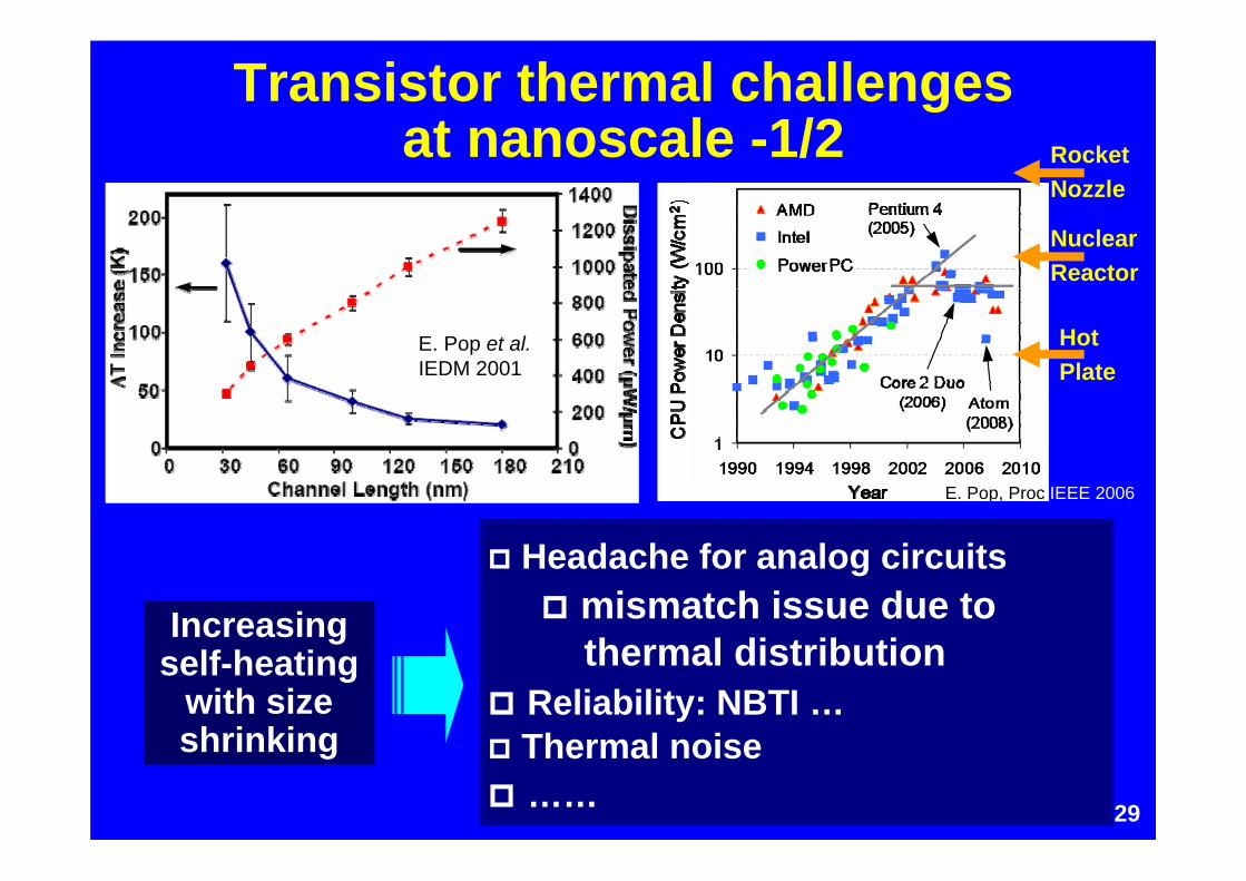
Transistor thermal challenges at nanoscale -1/2
E. Pop et al.IEDM 2001
Rocket Nozzle
Hot Plate
Nuclear Reactor
Increasing self-heating
with size shrinking
Headache for analog circuits mismatch issue due to
thermal distribution Reliability: NBTI … Thermal noise ……
E. Pop, Proc IEEE 2006
30
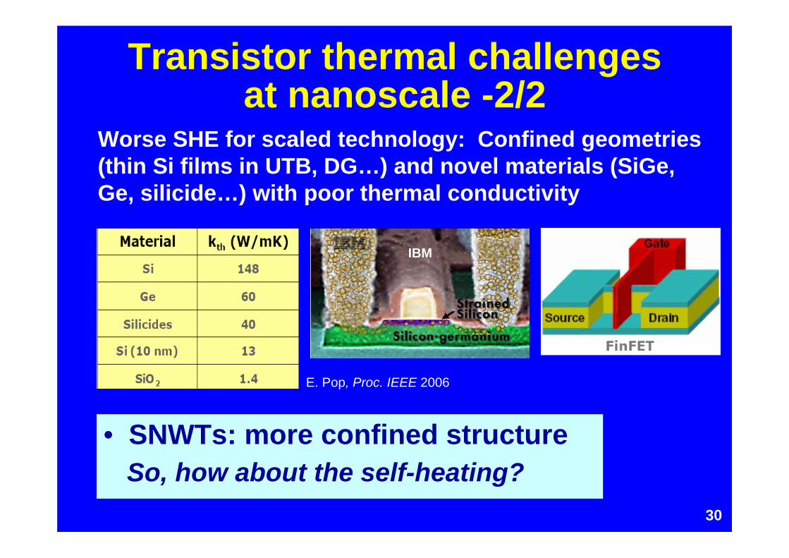
Transistor thermal challenges at nanoscale -2/2
Worse SHE for scaled technology: Confined geometries (thin Si films in UTB, DG…) and novel materials (SiGe, Ge, silicide…) with poor thermal conductivity
E. Pop, Proc. IEEE 2006
• SNWTs: more confined structureSo, how about the self-heating?
IBM

31
SHE Characterization of SNWTs• AC conductance method
0.0 0.3 0.6 0.9 1.2 1.50
100
200
300
400
500Bulk SNWTsLG=130nm
Hollow: w/ SHE (DC)Solid: w/o SHE (AC)
VD (V)
I D (
A)
VG=1.2V
VG=1.5V
VG=1.8V
R. Wang, et al., IEDM 2008,PKU
SNWTs on fully bulk substrate (w/o e-SiGe S/D or SOI)

32
• SHE in SNWTs even on bulk-Si substrate is a little bit worse than SOI devices
Comparisons
[12] G. Guegan et al., Mater. Res. Soc. Symp. Proc., 2006; [13] K. Etessam-Yazdani et al., ITHERM, 2006; [14] B. M. Tenbroek et al., IEEE TED, 1996; [15] W. Jin et al., IEDM, 1999; [x] A.J. Scholten et al., IEDM 2009.
100 1000
10
100
SOI [13]
R
th (
mK
/mW
)
LG (nm)
Bulk SNWTs (this work)
Bulk [13]SOI [12]
SOI[14]
SOI [15]
0.01 0.1 1 100.1
1
10
100
Planar SOI [14]
T
(K)
Power (mW)
Bulk SNWTs (this work)
Planar SOI [12]
FinFET [x](on SOI)

33
Improvement by increasing heat dissipation through the gate stack?
• High-k gate dielectric has better thermal conductivity than SiO2 or SiON gate material
• but still have non-negligible SHE when dNW < 14nm
S. Bangsaruntip, et al., VLSI 2010
HfOx / TaN gate, LG=21nm

34
• 1D heat transport for strongly-confined NW structure– limited modes for heat dissipation
Why degraded SHE in SNWTs?
Source Drain
3D System System
Source Drain
TS TD
1-D heat transport
contact thermal resistance
q
BOX
TS TD
2-D heat transport

35
• 1D heat transport for strongly-confined NW structure– limited modes for heat dissipation
Why degraded SHE in SNWTs?
• Additional contact thermal resistance– abrupt interface between 1D-NW and 3D-S/D region – does not exist in planar devices
• GAA: increased surface/volume ratio, strong phonon-boundary scattering and thus increased boundary Rth– worse than UTB SOI, DG/TG structures
Source Drain
3D System System
Source Drain
TS TD
1-D heat transport
contact thermal resistance
q
BOX
TS TD
2-D heat transport

36
Thermal conductivity model for Si NWs
2
2 2
2
1
4
beff
b
b b
kkCA B
d d d L
[a] A. I. Hochbaum et al., Nature, vol. 451, p.163, 2008. [b] D. Li et al., APL, vol. 83, p. 2934, 2003. [c] P. Martin et al., PRL, vol. 102, p. 125503, 2009.
The model includes diameter dependence, surface roughness and gate length dependence.
X. Huang, et al., to be published.
0 40 80 1200
10
20
30
40
0 1 2 3 4 5
Roughness=1nm
k eff (
W/m
K)
Diameter(nm)
Roughness=0.3nm
stars: exp. [a,b]circles: simulation [c]lines: this work (model)
d=56nm
Roughness(nm)
d=115nm

37
Equivalent Thermal Network for SNWTs
Multi‐wires
in parallel
T=300K
T=300K
Rch2
Rch3
Rext1 Rext2Rs Rd
Rox
Rox
Rg‐pad
Rg‐sub
Rsub
Rcouple1
Rcouple2
Rch4
Rch1
Rox
Rox
Rox
RoxRcontact
Rd‐g
oxox Rcontact
X. Huang, et al., to be published.
0.0 0.3 0.6 0.9 1.2 1.50
100
200
300
400
500Line: model
I ds (u
A)
Red: wo/SHEBlack: w/SHE
Vds (V)
Bulk SNWTs LG=130nm
VG=1.8V
VG=1.5V
VG=1.2V
Symbol: Exp.
White
Symbol: ExperimentLine: model
Heat dissipation: to big S/Dto gate
38
Outline• Fabrication and integration (a quick review)• Recent advances in understanding SNWTs
– Intrinsic carrier transport– Parasitic effects (R and C)– Low-frequency noise– Self-heating effects– Variability
• Recent nanowire circuit demonstrations• Summary

39
• Variability challenges in nano-CMOS– new process technologies– new materials– much smaller devices
die-to-die
wafer-to-wafer
within-die
die-to-die
wafer-to-wafer
within-die
“There’s also plenty of noise and variation at the bottom…”
“There’s plenty of room at the bottom” -- Richard P. Feynman

40
Variation in nano-scale devices
• Random variations near atomic dimensions – impacts circuit functionality and stability
• New architecture NWFET with ultra-scaled dimension and surrounding gate structure– What about its variability?
Random Dopants, Line Edge Roughness, High-k Morphology, Metal Gate Granularity…
OPC, Layout Dependent Strain…
Random
Systematic

41
• Elimination of random dopant fluctuation (RDF) in the channel, what about other sources?
What about GAA nanowire MOSFETs?
DrainGate
Extension
Metal-gate WFVariation (WFV)
NW cross-
sectional
shape variation
(radius ∆R,
etc.)
Gate length ∆Lg
NWLER/LWR
Ext. length ∆Lext
Extension region RDF(Rext or Lext variation)
Transport (ballistic effects, mobility) variation due to strain variation, surface roughness, etc.
Source
NWChannel
Effective channel length ∆L:L
2 = Lext2 + Lg
2
New sources:diameter variation, NW LER/LWR, NW SDE RDF

42
Impacts of Variation Sources in SNWTs(Experimental Extraction Results)
100 200 300 400
Vgs=1.2VVds=1.2V
Lg (nm) I
on (a
.u.)
L R long
1,2
LER WF
Variation Sources
100 200 300 400
V
th (a
.u.)
Lg (nm)
Vds=1.2V L R long
1,2
LER WF
Variation Sources
J. Zhuge, et al., IEDM 2009,PKU
R WF LER, L
R

43
Discussion - 1/2: SDE RDF (1)implant variation near
the interface
RTA variation
R. Wang et al., T-ED 2011, p. 2864.PKU
5
10
15
20
25
Rto
tal
(dN
W/2
)2 (
m2 )
4 12 20 28 36 44Nanowire Diameter dNW (nm)
• Diameter-Dependent Annealing (DDA): thinner NW results in faster diffusion– Rext reduction and variation– Leff reduction and variation
3-D KMC simulations

44
Discussion - 2/2: SDE RDF (2)
0.0 0.3 0.6 0.9
10-12
10-9
10-6dNW=45nmVdd = 1V
dNW=10nmVdd = 1V
I d (A
)
Vg (V)0.0
2.0x10⁻⁶
4.0x10⁻⁶
6.0x10⁻⁶
8.0x10⁻⁶
1.0x10⁻⁵
0.0 0.3 0.6 0.910-11
10-9
10-7
10-5
0.0
1.5x10⁻⁵
3.0x10⁻⁵
4.5x10⁻⁵
6.0x10⁻⁵
0 5 10 15 20 250.00
0.05
0.10
0.15
0.20
0.25
0.30
SNWTsLg=40nmLspacer=20nm
R (nm)
(R
ext
R2 ) (
m2 )
dNW=10nm dNW=45nm

45
SNWT vs. planar MOSFET – Simulations -1/2
PlanarLg=32nm
SNWTsLg=32nm
PlanarLg=32nm
SNWTsLg=32nm
• SNWT-based SRAM cells– Larger NM and less variation of noise margin
• intrinsic channel and excellent SCE-suppression
46
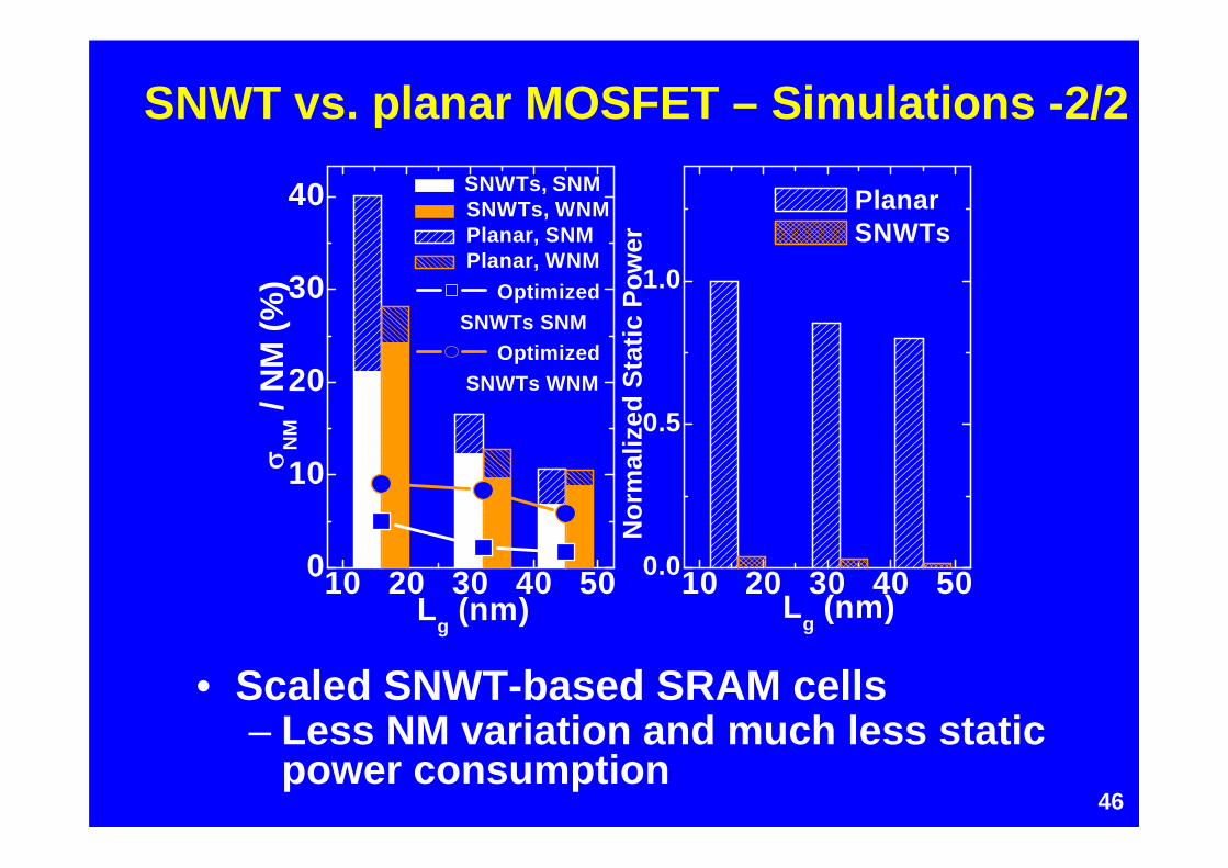
SNWT vs. planar MOSFET – Simulations -2/2
10 20 30 40 500
10
20
30
40
10 20 30 40 500.0
0.5
1.0 Optimized SNWTs SNM
Optimized SNWTs WNM
SNWTs, SNM SNWTs, WNM Planar, SNM Planar, WNM
Lg (nm)
NM /
NM
(%)
Planar SNWTs
Nor
mal
ized
Sta
tic P
ower
Lg (nm)
• Scaled SNWT-based SRAM cells – Less NM variation and much less static
power consumption

47
Comparisons with FinFET and UTB SOI Devices
• Experimental demonstrations so far
0
1
2
3
4
5
SNWTUTBSOI
FinFET
AVT
(mV-m
)
Planar bulk
Experimental data from 2007-2010 IEDM, VLSI papers
Samsung, VLSI 2008
With careful process control
effeff
VTT WL
AV

48
• First-order device-level comparisons with FinFETs
Main device characteristics Comparison with FinFETs

49
Outline• Introduction• Fabrication and integration• Recent advances in understanding
SNWTs– Parasitic effects– Self-heating effects– Variability
• Recent nanowire circuit demonstrations• Summary

50
• SRAM (Samsung, VLSI 08)– Larger SNM than planar and
FinFET devices– Smallest variation demo
• Current Mirror (Peking Univ., T-ED 11)– Good performance in both inversion and subthreshold
regions• 25-Stage Ring Oscillators (IBM, VLSI 10)
– dNW= 3~14 nm, LG= 25~55 nm– Limited by the SDE series resistance, need further
improvement
Circuit demonstration is at early stage

51
Outline• Introduction• Fabrication and integration • Recent advances in understanding SNWTs
– Parasitic effects– Self-heating effects– Variability
• Recent nanowire circuit demonstrations• Summary
52
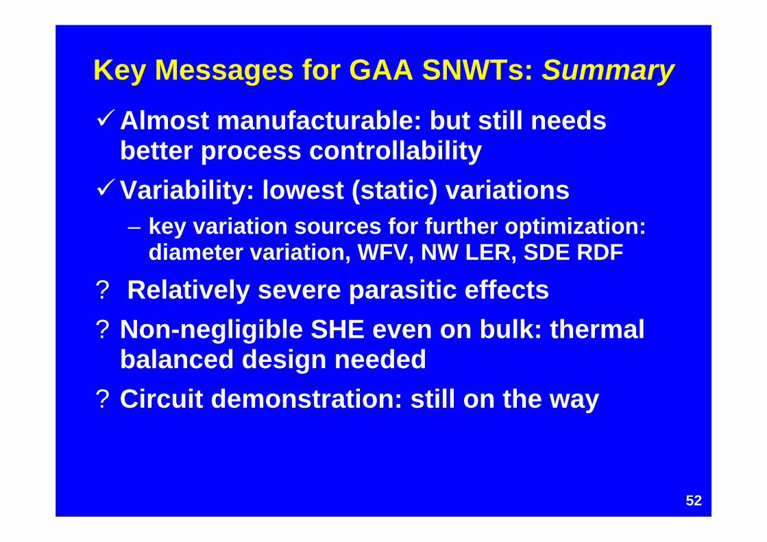
Key Messages for GAA SNWTs: SummaryAlmost manufacturable: but still needs
better process controllabilityVariability: lowest (static) variations
– key variation sources for further optimization: diameter variation, WFV, NW LER, SDE RDF
? Relatively severe parasitic effects? Non-negligible SHE even on bulk: thermal
balanced design needed? Circuit demonstration: still on the way

53
Source Drain
Drain Ext.
Gate
Source Ext.
Source Drain
Drain Ext.
Gate
Source Ext.
Quasi-1D cylindrical channel• transport• self-heating• reliability
Multiple surface orientations• reliability• noise
Strong confinement with GAA• transport• reliability• noise (RTN)
3D S/D interfaced with 1D NW• transport• self-heating• parasitics
Shallow SDE region• variability• parasitics• noise…
Structure features should be included
Further in-depth understanding and special device-circuit co-design expected

5454
Thank You Very Much !