gem detector assembly, implementation, data analysisdavid.gore/capstone/files/colvinlosada.pdf ·...
TRANSCRIPT

1
GEM Detector Assembly, Implementation,
Data Analysis
William C. Colvin & Anthony R. Losada
Christopher Newport University
PCSE 498W
Advisors:
Dr. Fatiha Benmokhtar (Spring 2012)
Dr. Edward Brash (Fall 2012)

2
ABSTRACT
In particle physics experiments, one of the crucial techniques for determining the energy
and momentum of the scattered particles produced in collisions is to use position-sensitive
detectors. These detectors, when used in combination, provide a "track" of the particle as it
travels outward from the collision point. The Gas Electron Multiplier (GEM), a type of position-
sensitive detector, shows great promise for future use at particle accelerators. In our project, two
prototype GEM detectors were assembled and tested in an experiment at the Italian National
Institute of Nuclear Physics (INFN) in Frascati, Italy. The GEM detectors were used to measure
the position/trajectory of the incoming electron beam which was used in conjunction with
another detector, known as a Ring Imaging Cherenkov Detector (RICH). In addition to building
the GEM detectors themselves, we were responsible for assembling a system of electronics that
could be used to signal an event, or when a charged particle passes through the detector.
Furthermore we calibrated the response of the GEMS, and aided in the subsequent data analysis.
We will report on all aspects of this process from construction to data analysis.

3
Table of Contents
Title Page ……………1
Abstract ……………..2
Table of Contents……3
Introduction………….4
Theory……………….5
Experiment…………..6
Construction…………7
Implementation………8
Efficiency……………9
Data Analysis………..11
Future Work…………13
Appendix…………….14
4
Introduction
For our PHYS 498 capstone project, we worked on the Ring Imaging Cherenkov (RICH)
detector upgrade being constructed for Experimentation Hall B at Thomas Jefferson National
Accelerator Facility (TJNAF). This project was an international collaboration with the Italian
National Institute of Nuclear Physics (INFN) in Frascati, Italy. The RICH detector consists of
two main parts. The first is two Gas Electron Multiplier (GEM) detectors that are used to plot
trajectory of a charged particle. The two GEM detectors are not part of the actual RICH but
rather will be used for the prototype only. The second part if the RICH detector itself consists of
an aerogel block, used as a Cherenkov radiator combined with an array of Photomultiplier Tubes
(PMTs), used to detect the Cherenkov cone. When first offered to join this collaboration we
were given two separate tasks; William would set the electronics for the GEMs and operate
them. Anthony would write macros to read and display the data collected by 28 PMTs. However,
it was crucial that we both know the specifics of each other's work. This is because, in Italy we
were both expected to be able to answer any question asked about either project as both of were
not always present. Once problems arose with the arrival of the GEMs, Anthony was reassigned
to the GEM portion of the RICH upgrade, joining William’s work. At this point, the goals were
set as follows:
1. Assemble the two GEMs.
2. Calibrate and test them at TJNAF.
3. Operate them on the beam line at INFN.
4. Collect successful run data to be analyzed upon return to the TJNAF.
5. Calculate the position of the beam line with respect to the GEM detectors.

5
Theory
Gas Electron Multipliers (GEMs) are a type of micro pattern detectors created by CERN
in 1997. The key element to the GEMs is the four pieces of very thin double-sided copper-clad
kapton foil (See Figure 4). The foil is perforated with a high density of holes, and each hole has a
diameter of about 70 µm and spaced 140 µm apart (center-to-center). A gas mixture of 70%
argon and 30% carbon dioxide is left to flow through the chamber at a very low pressure so that
the kapton foil is not damaged. A high voltage, no greater than 4.1kV, was applied to the drift
chamber of the GEMs. This voltage created a potential difference between the stacked layers of
kapton foil and the signal strips. In order to trigger the data acquisition software to record the
voltages on the signal strips, a trigger must be set up. The most common trigger setup is a pair of
scintillators, one in front and one behind the GEM chamber. A charged particle travels through
the front scintillator and the outer layer of the GEM and then, temporarily neglecting diffusion,
the particle follows the electric field lines created when a potential difference is introduced to the
front and back electrodes. These lines are then pushed into the holes of the kapton foil, in what is
called the drift region (See Figure 11). The high electric fields in these holes excite the particle
and thus it causes a coulomb interaction with the gas and the medium is ionized releasing an
electron-ion pair. As a result of the high electric field, the field lines multiply causing the
primary electrons to further ionize the gas, thus creating secondary electrons. This then causes an
avalanche effect where each new electron is interacting with the medium, resulting in an
exponential increase in electron quantity (See Figure 7). These charges can then be picked up by
sensors with 256 channels for both x and y positions located on the board at the base of the GEM
(See Figure 3). Depending on the equipment set-up and the Data Acquisition (DAQ) System,
GEMs can be used to analyze different scenarios. A common use of GEM detectors is to
6
calculate a beam track. This is done by placing a minimum of two chambers in parallel one in
front of the other, collecting the x and y position of where the beam passed through each
chamber, and then calculating the slope. This slope calculation was crucial for the success of the
RICH detector prototype. In order to find the most accurate beam trajectory through the RICH,
the GEMs would need to “sandwich” the aerogel and PMT array.
Experiment
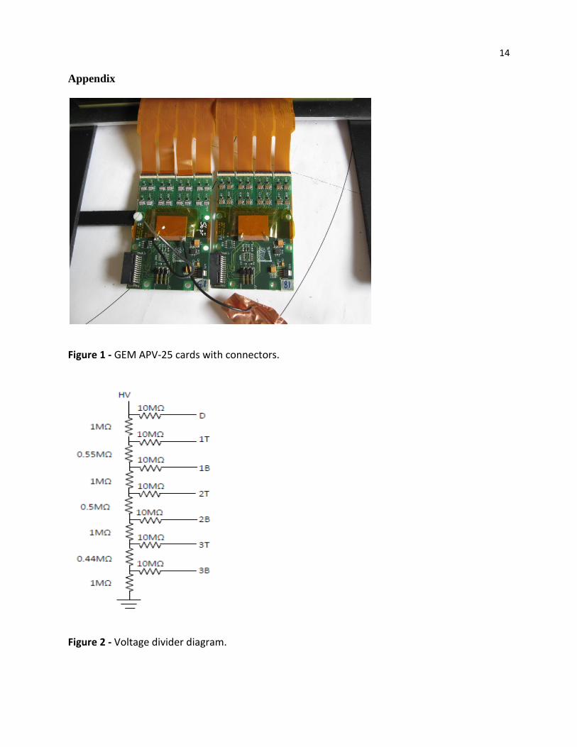
Our preparation for the experiment began in early 2012. The first task was to acquire two
Panasonic adapting connectors for each chamber. These are needed because the readout chips
used at CERN are not the same as APV-25 readout chips used in Frascati. Each connector has
128 channels, so two connectors are needed for the x and y positions respectively. A picture of
these connectors and the APV-25 cards can be seen in Figure 1 in the Appendix. This connector
had to be specially fabricated and purchased by TJNAF. The next task was to build two voltage
dividers, making one for each chamber. A voltage divider is a series of resistors used to split up a
high input voltage. The output voltage is a fraction of the initial voltage and the ratio is
dependent on the resistors used. Voltage dividers are essential to the GEM detectors because
without them a discharge voltage between the layers of kapton would likely destroy the chamber.
With a voltage divider applied, the discharge would cause a drop in one of the voltages which
would cause the overall voltage to decrease and prevent damaging high electric fields in the drift
region. A diagram of the voltage dividers can be seen in Figure 2.
Upon arrival of the GEMs, we encountered our first large setback. Our expectation was
that the GEMs would arrive ready to be run; only lacking the APV-25 electronics setup and
voltage dividers. However, what we received was a parts kit, for two unassembled GEM

7
detectors. This meant our focus had to switch from calibration of the GEMs, to construction.
Construction
While we understood the basic concepts of GEMs, we needed the help of an expert in
order to avoid damaging them. So we emailed UVA asking for help and one of their grad
students, Kiad, walked William through the assembly at TJNAF. To begin, the chamber wall had
to have the gas inputs attached and sealed (See Figure 5). This was done with a twenty-four hour
epoxy. Using the same epoxy, the translucent plastic “window” was sealed to the cover of the
GEM (See top of Figure 4). Then four plastic rods were glued onto the board to support the
Kapton frames. These rods were glued with a five minute epoxy. The layers were then placed
onto the board and supported with the plastic rods. ½ mm plastic spacers were used to create a
gap between the layers. With the frames that protect the foils having a ½ mm thickness on the
top and bottom, two spacers were used to create a 2mm gap between the layers. The gap between
the board and the bottom foil requires 3 spacers because there is no frame to provide the extra ½
mm on the board. The distance between the third layer and the drift foil is larger, using four
spacers to make a 3mm gap between the layers. Both the top and bottom sides of the foil strip
must be soldered to the board via the copper strips. While there is no specific strip designated for
each layer, it is vital that each side of each layer is on its own strip. It is also necessary to know
where each layer is attached when implementing the voltage divider. Once the chamber wall had
finished drying, two rubber tubes were used as O-rings for the top and bottom of the wall
respectively. The wall was then placed onto the board encasing the foils and the top cover was
then bolted on and tightened to ensure a thorough seal. During this process nitrogen gas running
through a filter was used to clean off every part of the detectors throughout the construction. It

8
was absolutely necessary to perform the entirety of this construction within a clean-room to
prevent dust from getting into the sealed chamber. See Figure 6 for the completed GEM rig.
Once the GEMs themselves were constructed the voltage dividers were installed. This
was a quick task of soldering the voltage dividers in place. To ensure everything was connected
properly, we used a multi-meter to check for short circuits. After confirming there were none, we
ran 4.1 kV through it and tested the current output to verify we were creating the proper electric
field. At this point the GEMs were ready to be tested using TJNAF’s facilities, which would be
done one at a time due to resource constraints.
Implementation
In order to test the GEMs we had to set up the coincidence trigger. To do this we placed a
GEM between two scintillators. Using a coincidence module the trigger logic was set to only
accept a hit if it occurred on both scintillators simultaneously. A discriminator was used and set
to accept any trigger greater than or equal to 30 mV. When a coincidence was accepted and the
signal was above 30 mV a veto was set to prevent further signals from being read. While the veto
was active a read-out module read the data from the APV-25 cards and sent it to the Data
Acquisition System (DAQ). When the DAQ finished processing the hit, it sent a reset command
back to the veto module which turned the veto off. The cycle then repeated from there once a
new hit was registered (See Figure 8).
With the two GEM detectors were constructed and all external electronics had been set
up, we began the process of testing. To act as a source we placed a small amount of Strontium-90
above the top scintillator. As the Strontium-90 underwent radioactive decay, it would release a
beta particle. This beta particle would pass through the top scintillator, the GEM chamber, and
then the bottom scintillator, triggering a coincidence event and creating an electron avalanche in

9
the GEM. However, beginning with our first run we experienced an extraordinarily large amount
of background noise. This noise created inefficiency and reducing it became the focus of our
calibration efforts.
Efficiency
We were told by Evaristo Cisbani that the GEM detectors should ideally be over 99%
efficient with a common background noise of around 10-30 ADC units. An ADC unit is
proportional to the voltage detected on the strips; this proportion is caused by the process of
analog-to-digital conversion, thus the name ADC. Efficiency is defined as the number of “good”,
or usable, hits divided by the total number of samples. Over the course of the experiment, the
average background noise we registered was around 500 ADC units, 50 times greater than
expected. While the background noise was capable of blocking the analysis programs from
detecting hits, we should have been able to see them by eye on the display modules. However,
when we check we saw only a few over the course of several samples, meaning not only was
there background noise, but some other causes of inefficiency as well. With the aid of Mark
Jones at TJNAF, and Evaristo Cisbani at INFN, we identified and attempted to correct several
causes of inefficiency.
The first inefficiency cause we tackled was the large amount of background noise. As
stated above, the GEM should have a background noise of 10-30 ADC units and we were
experiencing 500 ADC units. To solve this problem we tried four main solutions. First we added
layers of insulation between the electronics (such as the ADC cards) and the metal rack the
GEMs were in. This resulted in no noticeable change. Second, we placed the GEMs in a faraday
cage in an attempt to reduce interference from electric fields. This gave us a visible change,
dropping the average background radiation by 50-100 ADC units. The third solution attempt was
10
to add extra grounding. The key in doing this was to avoid creating loops that could feed ground
signals from one APV card into another. The added grounding also produced positive results,
lowering the background by another 100 ADC units. At this point our background noise was
averaging at 300-350 ADC units, which was still too high. Our final solution was to simply
increase the distance between the GEMs and other sources of electronic interference. We moved
the GEMs two meters from everything else and our background noise dropped to less than 50
ADC units. The reason this was so effective is due to the fact that electromagnetic interactions
decrease by 1/R2.
With the background noise problems solved, we expected to begin seeing a high
efficiency, but it was still far below 50%. There were a few possible causes for this. The next
potential problem we decided to solve was what is known as clocking errors. Due to the speed in
which the charged particles are moving, sampling has to be correct within 50ns. The time it takes
for the electric signals to move across wires creates a latency effect that can cause our sampling
to be late. To account for this, clock settings are added to programs to go back through older data
for sampling. A clocking error occurs when this window is offset from the good data. To solve it
we simply set the phase clocks to zero and took data runs, incrementing the clock in steps of
25ns as we went. Eventually we started seeing consistent hits, verifying our clock settings (in our
case this occurred at around a 450 ns delay). With the clocks fixed our efficiency rose, but was
still around 30%.
The final issue that caused problems during the experiment was improper gas flow. In our
case, the gas flow was so low that the GEMs efficiency was cut by over half. Once discovered,
this issue was easily fixed by quadrupling the gas flow. The reason this occurred was due to the

11
electronic flow-meter not having any form of units for its flow rate. This solution brought our
final efficiency to just below 80%.
Data Analysis
In order to begin the process of analyzing data, we first had to take what is known as a
pedestal run. This is a data collection run taken using a false trigger, at a point when no charged
particles were being sent through the GEMs. The purpose of this run is to find the average levels
of background noise on each channel. As long as that noise is within an acceptable level, the
pedestal run will be a baseline. A background noise of less than 100 ADC units is usable, but less
than 50 is desirable. The pedestal run will be subtracted from all future data runs taken under the
same conditions.
Once a pedestal has been set, the runs with data may be analyzed. We used two methods
of data analysis. The first method is what we will refer to as “live analysis”. For a live analysis,
we would begin looking at data while the acquisition program was still running. Once it had 50+
hits we would load the data into a root tree and plot the immediate voltage on the strips at a 25ns
time step for the 150ns following the trigger. The purpose of doing this was to simply check for
good hits by eye. We would expect to see a voltage spike up to 1000 ADC units then a slow
decay over the course of the 150ns. The main purpose of doing this was to ensure that the GEMs
were operating properly. Therefore, this was our main method of analysis throughout the
experiment both at TJNAF and INFN. This was the method used to calibrate the GEMs, by
making small changes to a single setup variable, such as the phase clock. We could take several
different runs within a small time frame and check to see which parameters produced the best
results.

12
The other type of analysis is what is called “reconstruction” analysis. This analysis is
what we spent the majority of the fall term learning how to do and trying to make functional. The
process behind the reconstruction program is a fairly straightforward process in theory, but
becomes complex in practice. In his “Note on GEM reconstruction for CERN Test”, Evaristo
Cisbani explained the process in seven steps.
1. Find the strip with the maximum charge. Define as X
2. Define three windows surrounding X (See Figure 9)
a. Peak region (X±n)
b. Near region (X-2n, X-n) and (X+n, X+2n)
c. Background region (0, X-2n) and (X+2n, 127)
3. Compute the integral of the peak region. Define as SP
4. Compute the mean of the near region. Define as MN
5. Compute the RMS of the background region. Define as RMSB
6. Check to see if the hit is a “good” hit. (Sp- 2n*MN)>(nsigma*RMSB)
7. If defined as a good hit, the peak region is fitted with a Gaussian. The center
point of the Gaussian is defined to be XG. (See Figure 10)
When performing these calculations with the 10cm by 10cm GEM detectors, n is always
assumed to equal to five. The second unlabelled value, nsigma, is the “noise threshold number of
the RMS”, which is always set as 4. These steps, 1 through 7, are performed for every sample of
an event. For an event to be usable, the following two conditions must be met:
1. At least three of the samples are defined as good hits (step 6 returns true).
2. XG differs by no greater than 1 millimeter between all of the good hits.

13
If the event is usable, we average the XG of each sample, and that value becomes the coordinate
position, either x or y depending on the plane, for that event. This process is repeated for the
same event on each plane of both GEMs. If the event is usable on all four planes, then the (X,Y)
coordinates for both GEMs are printed out to a file to be used for beam tracking. This entire
process is repeated for every event to fill the file. With these coordinates, it is now possible to
plot the trajectory of the slope.
Future Work
Given more time to work with the project, there are several things we would like to have
done. Due to the focus of the collaboration being on the RICH detector, the programs we used
were designed to pull necessary data from the GEMs, but not display it. The first thing that could
be done is to write a program that displays the “good” hits in a two dimensional histogram
representing the face of the GEM. This program would also plot or print the vector trajectory of
the beam line using the distance between the two GEMs as the third dimension. Additional future
research would focus on maximizing the efficiency of the GEMs. During the experiment we had
constant struggles with noise, and tried several ways to reduce it. Eventually we were forced to
place the GEM detectors about two meters away from the other electronics. The required
distance from electronics may be effective, however, it is not an ideal setup. Given more time,
we would like to experiment with the causes of background noise and find different methods of
reduction. Ultimately, the goal would be to control noise in a way that allows the GEM detectors
to be used in close proximity (<.5m) to other electronics.
14
Appendix
Figure 1 - GEM APV-25 cards with connectors.
Figure 2 - Voltage divider diagram.

15
Figure 3 - GEM board.
Figure 4 - Kapton foils with frames and translucent window.

16
Figure 5 - Open GEM with chamber wall and gas inputs.
Figure 6 - Completed GEM rig on the beam line.

17
Figure 7 - Diagram of an electron avalanche.
Figure 8 - Trigger logic diagram.
Scintillators
Coincidence
Veto on Pipeline sampled
Veto Off

18
Figure 9 – Picture of hit display with regions defined.

19
Figure 10 – Hit display with Gaussian fit on the good hit.

20
Figure 11 – An illustration of the electric field lines in a hole within the kapton foil.