generating mif files - computer science &...
TRANSCRIPT

Generating MIF files
Introduction In order to load our handwritten (or compiler generated) MIPS assembly problems into our instruction ROM, we need a way to assemble them into machine language and then save these machine language programs in a text file where the binary machine instructions are represented as a sequence of ASCII hexadecimal values. For this, we will use a Java-based MIPS simulator called MARS. MARS is an improved version of the SPIM simulator that you may have used in CSCE 212. We have installed MARS in a shared directory, but in order to avoid the need to specify its entire path, you can specify a UNIX alias to make it more convenient to run MARS. Open a terminal and type gedit .profile. In the text editor, add the following line to the end of file: alias mars='java -jar /usr/local/3rdparty/csce611/MARS/Mars.jar' Save the file and close the editor. You will only need to do this once. Now log out and log back into your workstation. Now we can invoke the tool by typing mars in the terminal. You can also download MARS from www.cs.missouristate.edu/MARS or get a copy at your home directory. For the usage of the simulator, please check the MARS tutorial at http://courses.missouristate.edu/KenVollmar/MARS/tutorial.htm MIF Files A memory Initialization File (.mif) is an ASCII text file (with the extension .mif) that specifies the initial content of a memory block (CAM, RAM, or ROM), that is, the initial values for each address. This file is used during Quartus project compilation and/or simulation. The MIF file serves as an input file for memory initialization in the Quartus compiler and simulator. You can also use a Hexadecimal Intel-Format File (.hex) to provide memory initialization data. In this class, we provide you with a script file to automate generate MIF file from MIPS assembly codes. In this tutorial, we will introduce you to MIF file generation in the following example. 1. Open a terminal and copy the file GenMIF.sh from the directory /usr/local/3rdparty/ csce611/CPU_support_files/ to your design directory. 2. For our first program, copy the following file into your home directory:

cp /usr/local/3rdparty/csce611/benchmarks/my_program.asm
3. In order to show you what the program looks like, open this file in a text editor: gedit my_program.asm
As you will see, this program is composed of a data section and a text (code) section. Our script will generate MIF files for both sections, which correspond to the data memory and the instruction memory, respectively. Also notice that this particular program is quite simple and is composed entirely of load instruction and a branch at the end which is clearly being used to halt the program by deliberately entering into an infinite loop. The reason for this is because in the following tutorial, we will implement the load instructions and the branch instruction used in this program. It will be up to you to implement the other instructions listed in the MIPS instruction set detail on the course webpage. 4. Generate the MIF files using the following command: ./GenMIF.sh my_program
You should see the following messages: Reading file my_program.asm Generating ROM1.mif Generating RAM1.mif Generating RAM2.mif Generating RAM3.mif Generating RAM4.mif Memory MIF file generation successful.
and you should have the following .mif files in the my_program subdirectory: ROM1.mif, RAM1.mif, RAM2.mif, RAM3.mif and RAM4.mif At this point, the generics in your ROM and RAM instances should point to the ROM and RAM MIF files that you just generated. Congratulations, you have just loaded a program into your computer! Now it’s time to begin to work on your CPU design so you can implement the instructions used in this program.

Implementing the MIPS Instruction Set In this tutorial we’ll be adding functionality to the CPU design. Instancing Primary Components to Your Top-Level CPU Design In order to implement the load and branch instructions, we’ll need a few basic components. These will include:
an ALU
a register file
a program counter (PC)
a PC incrementer adder
a PC branch target adder Instantiate the ALU that you have previously designed, as well as the RegFile32x32, reg10, and two add10s from the CSELib.
Program Counter Logic Some of these components have fairly obvious connections. For example, we know that the PC keeps track of the address of next instruction to be fetched, so we need to connect it to the instruction address output. However, since we also need to use the output of the PC to increment the PC, we cannot directly tie the output of the PC register to the output pin, because this would involve “reading an output” which VHDL forbids. Therefore we will need to

create a signal called “PC” for this, which we can rename to InstructionAddr using an embedded block. Also, we know that the PC’s input can come from either the PC incrementer adder or the branch target adder. So let’s add an embedded multiplexer (as you did for the logical unit in the ALU) to the input of the PC, and connect the PC incrementer adder (which computes PC+1) and the branch target adder. Also, you need to connect the PC to the global clock and reset signals. You may want to do this through “signal stubs” with implicit connections. Finally, we will use the same embedded block that we used to rename the PC signal for setting some constants, which we’ll need for ALU carryin inputs (CI), the PC enable, and the input for the PC incrementer.
Register File and ALU Next let’s deal with the register file. We know that the ReadAddrA and ReadAddrB inputs come directly from the rs and rt fields of the instruction, so we can connect those signals using bus rippers. Recall that we’re only implementing the BEQ instruction and the load instructions at this time. Of these, only the load instructions write to the register file. As a result, we know the WriteData input to the register file comes from the data memory input. However, since we’ll

need to design a data alignment unit for the LH and LB instructions, we’ll just add a signal stub for now, named “DataInAlignedExt”. The WriteAddr input to the register file comes directly from the rt field, so we can make this connection as well. You can also connect the outputs of the register file directly to the ALU inputs. The register file write enable will be named “RegWrite_WB” since this signal is part of the Write-Back pipeline stage. For the ALU’s shift amount input, you may connect InstructionIn(10 downto 6) for now. However, in the future you will need to multiplex this input to support the variable shift instructions (i.e. sllv, srlv and srav).
Load Alignment and Extension Logic Now we’ll design the load alignment and sign/zero extension logic. After a load instruction is fetched, let’s assume the control unit will drive a signal called “load_type” with the following encodings:
Instruction load_type
LW 000
LH 001
LHU 010
LB 011
LBU 100
Set up your design as shown below:
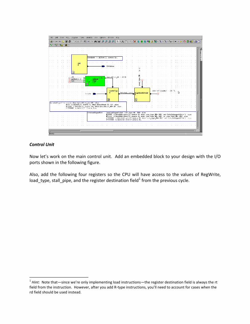
Control Unit Now let’s work on the main control unit. Add an embedded block to your design with the I/O ports shown in the following figure. Also, add the following four registers so the CPU will have access to the values of RegWrite, load_type, stall_pipe, and the register destination field1 from the previous cycle.
1 Hint: Note that—since we’re only implementing load instructions—the register destination field is always the rt
field from the instruction. However, after you add R-type instructions, you’ll need to account for cases when the rd field should be used instead.

Now we can design the actual control unit. Double-click the embedded block and choose Truth Table as the view type. The main function of the control unit is to decode instructions into a set of control signals, which are distributed to various components in the CPU and establish datapaths for executing each instruction. Control signals are usually made up of multiplexer selects and write enables. We will design one monolithic control unit that will control all aspects of the CPU, including the ALU control and branch control (recall that Hennessy and Patterson’s design had separate control units for these functions). At this point we will enter control signals for six instructions: LW, LH, LHU, LB, LBU, and BEQ. According to the instruction set detail, these instructions have the following control information encoded into their machine-language representations:
Instruction Opcode (bits 31:26)
LW 100011
LH 100001
LHU 100101
LB 100000
LBU 100100
BEQ 000100
Design the control unit truth table as shown below.

For reference a complete CPU design is shown in the following figure.
Verifying the CPU At this point our CPU is finished. Let’s simulate it. More specifically, we need to simulate the “MyComputer” design, because it contains the instruction memory , which we need to provide our CPU with a workload. So make you simulate the “MyComputer” design hierarchically and not just the CPU itself.
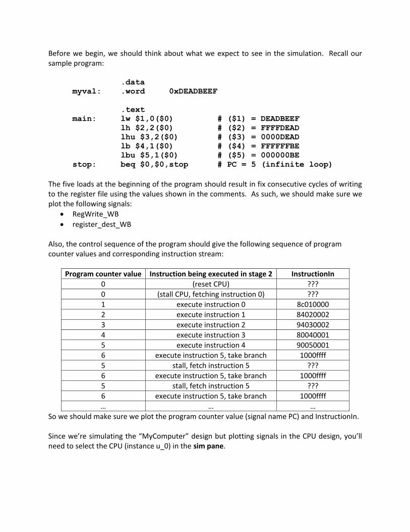
Before we begin, we should think about what we expect to see in the simulation. Recall our sample program:
.data
myval: .word 0xDEADBEEF
.text
main: lw $1,0($0) # ($1) = DEADBEEF
lh $2,2($0) # ($2) = FFFFDEAD
lhu $3,2($0) # ($3) = 0000DEAD
lb $4,1($0) # ($4) = FFFFFFBE
lbu $5,1($0) # ($5) = 000000BE
stop: beq $0,$0,stop # PC = 5 (infinite loop)
The five loads at the beginning of the program should result in fix consecutive cycles of writing to the register file using the values shown in the comments. As such, we should make sure we plot the following signals:
RegWrite_WB
register_dest_WB
Also, the control sequence of the program should give the following sequence of program counter values and corresponding instruction stream:
Program counter value Instruction being executed in stage 2 InstructionIn
0 (reset CPU) ???
0 (stall CPU, fetching instruction 0) ???
1 execute instruction 0 8c010000
2 execute instruction 1 84020002
3 execute instruction 2 94030002
4 execute instruction 3 80040001
5 execute instruction 4 90050001
6 execute instruction 5, take branch 1000ffff
5 stall, fetch instruction 5 ???
6 execute instruction 5, take branch 1000ffff
5 stall, fetch instruction 5 ???
6 execute instruction 5, take branch 1000ffff
… … …
So we should make sure we plot the program counter value (signal name PC) and InstructionIn. Since we’re simulating the “MyComputer” design but plotting signals in the CPU design, you’ll need to select the CPU (instance u_0) in the sim pane.

Selecting u_0 will show all the CPU’s signals in the Object pane, allowing you to add to them to wave window by right-clicking the signals or dragging them into the wave window. Note that you can also add signals from the block diagram editor using the toolbar on the bottom of the window. Once you’ve added the signals above--as well as clk and rst—convert all signals to hexadecimal. Also, click the “mountains” button at the bottom of the wave window to switch the signal names to their shortened representations.
There is one last step before we run the simulation. We need to set up the clock signal and perform a manual reset. To set up the clock, right-click “clk” in the wave window, select “Clock…”, and click OK.

To perform a manual reset, make sure the CPU (u_0) is highlighted in the sim pane, then enter the following commands into the Modelsim console:
force –freeze rst 1
run
force –freeze rst 0
run 1000
Alternatively, we can use ModuleWare to generate the above input stimuli for simulation. In the Design Manager right-click the Design Unit MyComputer and in the pop-up menu select New -> Test Bench… Then click OK in Create Test Bench dialog box. Double-click the newly created Design Unit MyComputer_tb and delete the light-blue component in the block diagram view of the MyComputer_tb. Then choose Add ModuleWare button to add Clock and Pulse components from the Stimulus directory.

Double-click the instantiated modulewares and change the default settings as follows. Note the Clock Edge Times must be at least 100 ns for the positive pulse to be sampled by the rising clock edge.
Let’s simulate the CPU design by saving the Block Diagram view, highlighting MyComputer_tb in the Design Manager and launching Modelsim. What to do Next You now have a 3-stage pipelined CPU design, along with instruction and data memories that can be initialized within simulation and even after being implemented on an FPGA. However, your CPU is currently only capable of executing programs that are composed entirely of limited subset of instructions that includes the load instructions and the BEQ instruction. Your goal is to extend this CPU design such that it can execute all the MIPS instructions listed in the instruction set detail on the course webpage. To do this, you will need to add multiplexers, control signals, and rows to the control unit truth table. You will be able to test instructions as you add functionality for them by using the MARS design flow to write programs that contain those instructions.

We will test your CPU design by loading a program called SimpleTest that contains at least one instance of every instruction in the instruction set.