gl9701 datasheet 090 - computex taipei · datasheet revision 0.90 sep. 05, 2006 ... fax: (886-2)...
TRANSCRIPT

GL9701
PCI ExpressTM to PCI Bridge
Datasheet Revision 0.90 Sep. 05, 2006
Genesys Logic, Inc.
GL9701 PCI ExpressTM to PCI Bridge
©2000-2006 Genesys Logic Inc. - All rights reserved. Page 2
Copyright: Copyright © 2006 Genesys Logic Incorporated. All rights reserved. No part of the materials may be reproduced in any form or by any means without prior written consent of Genesys Logic Inc..
Disclaimer:
ALL MATERIALS ARE PROVIDED "AS IS" WITHOUT EXPRESS OR IMPLIED WARRANTY OF ANY KIND. NO LICENSE OR RIGHT IS GRANTED UNDER ANY PATENT OR TRADEMARK OF GENESYS LOGIC INC.. GENESYS LOGIC HEREBY DISCLAIMS ALL WARRANTIES AND CONDITIONS IN REGARD TO MATERIALS, INCLUDING ALL WARRANTIES, IMPLIED OR EXPRESS, OF MERCHANTABILITY, FITNESS FOR ANY PARTICULAR PURPOSE, AND NON-INFRINGEMENT OF INTELLECTUAL PROPERTY. IN NO EVENT SHALL GENESYS LOGIC BE LIABLE FOR ANY DAMAGES INCLUDING, WITHOUT LIMITATION, DAMAGES RESULTING FROM LOSS OF INFORMATION OR PROFITS. PLEASE BE ADVISED THAT THE MATERIALS MAY CONTAIN ERRORS OR OMMISIONS. GENESYS LOGIC MAY MAKE CHANGES TO THE MATERIALS OR TO THE PRODUCTS DESCRIBED THEREIN AT ANY TIME WITHOUT NOTICE.
Trademarks:
is a registered trademark of Genesys Logic, Inc. All trademarks are the properties of their respective owners.
Office: Genesys Logic, Inc. 12F, No. 205, Sec. 3, Beishin Rd., Shindian City, Taipei, Taiwan Tel: (886-2) 8913-1888 Fax: (886-2) 6629-6168 http://www.genesyslogic.com

GL9701 PCI ExpressTM to PCI Bridge
©2000-2006 Genesys Logic Inc. - All rights reserved. Page 3
Revision History
Revision Date Description
0.90 2006/09/05 First formal release
GL9701 PCI ExpressTM to PCI Bridge
©2000-2006 Genesys Logic Inc. - All rights reserved. Page 4
TABLE OF CONTENTS
CHAPTER 1 GENERAL DESCRIPTION.................................................... 9 CHAPTER 2 FEATURES ............................................................................ 10
2.1 PCI EXPRESS FEATURES........................................................................ 10 2.2 PCI INTERFACE FEATURES ................................................................... 10 2.3 POWER MANAGEMENT .......................................................................... 10 2.4 SMBUS INTERFACE ............................................................................... 11
CHAPTER 3 PIN ASSIGNMENT ............................................................... 12 3.1 PIN CONFIGURATION ............................................................................. 12 3.2 PINOUT.................................................................................................. 13 3.3NUMERIC PIN ASSIGNMENT LIST ........................................................... 14 3.4 SIGNAL DESCRIPTION ............................................................................ 16
3.4.1 PCI-Express Interface.................................................................. 16 3.4.2 Secondary PCI Interface.............................................................. 17 3.4.3 EEPROM Signals ......................................................................... 18 3.4.4 Miscellaneous Signals ................................................................... 18 3.4.5 Power and Ground Signals .......................................................... 19
CHAPTER 4 BLOCK DIAGRAM............................................................... 21 CHAPTER 5 FUNCTION DESCRIPTION ................................................ 24
5.1 POWER MANAGEMENT .......................................................................... 24 5.1.1 PCI-PM Software Compatible Power Management .................. 24 5.1.2 Hardware-Controlled Active State Power Management............ 24 5.1.3 In-band Beacon............................................................................. 24 5.1.4 Side-band WAKE_N .................................................................... 25 5.1.5 Power Management System Messages ........................................ 25
5.2 PCI CLOCK RUN.................................................................................... 25 5.3 PCI CLOCK............................................................................................ 25 5.4 INTERRUPT MAPPING ............................................................................. 26 5.5 INITIAL FLOW CONTROL ADVERTISEMENTS ......................................... 27 5.6 IDSEL MAPPING ................................................................................... 28
CHAPTER 6 REGISTER DESCRIPTION................................................. 29 6.1 OFFSET 00H: DEVICE IDENTIFICATION.................................................. 34 6.2 OFFSET 04H: COMMAND REGISTER ...................................................... 34 6.3 OFFSET 06H: STATUS REGISTER............................................................ 35
GL9701 PCI ExpressTM to PCI Bridge
©2000-2006 Genesys Logic Inc. - All rights reserved. Page 5
6.4 OFFSET 08H: REVISION ID .................................................................... 37 6.5 OFFSET 09H: CLASS CODE..................................................................... 37 6.6 OFFSET 0CH: CACHE LINE SIZE REGISTER ........................................... 38 6.7 OFFSET 0DH: PRIMARY LATENCY TIMER REGISTER............................. 38 6.8 OFFSET 0EH: HEADER TYPE REGISTER................................................. 38 6.9 OFFSET 0FH: BIST REGISTER................................................................. 38 6.10 OFFSET 10H: BASE REGISTER0............................................................ 38 6.11 OFFSET 14H: BASE REGISTER1............................................................ 38 6.12 OFFSET 18H: PRIMARY BUS NUMBER REGISTER................................. 39 6.13 OFFSET 19H: SECONDARY BUS NUMBER REGISTER ............................ 39 6.14 OFFSET 1AH: SUBORDINATE BUS NUMBER REGISTER......................... 39 6.15 OFFSET 1BH: SECONDARY LATENCY TIMER REGISTER ...................... 39 6.16 OFFSET 1CH: IO BASE AND IO LIMIT REGISTER................................. 39 6.17 OFFSET 1EH: SECONDARY STATUS REGISTER ..................................... 40 6.18 OFFSET 20H: MEMORY BASE AND LIMIT REGISTER ........................... 42 6.19 OFFSET 24H: PREFETCHABLE MEMORY BASE AND LIMIT REGISTER . 42 6.20 OFFSET 28H: PREFETCHABLE BASE UPPER 32-BITS REGISTER........... 43 6.21 OFFSET 2CH: PREFETCHABLE LIMIT UPPER 32-BITS REGISTER ......... 43 6.22 OFFSET 30H: IO BASE AND LIMIT UPPER 16-BITS REGISTER.............. 43 6.23 OFFSET 34H: CAPABILITIES POINTER REGISTER ................................ 43 6.24 OFFSET 3CH: INTERRUPT LINE REGISTER........................................... 44 6.25 OFFSET 3DH: INTERRUPT PIN REGISTER ............................................. 44 6.26 OFFSET 3EH: BRIDGE CONTROL REGISTER......................................... 44 6.27 OFFSET 70H: PCI EXPRESS CAPABILITY LIST REGISTER.................... 48 6.28 OFFSET 72H: PCI EXPRESS CAPABILITIES REGISTER ......................... 48 6.29 OFFSET 74H: PCI EXPRESS DEVICE CAPABILITIES REGISTER............ 49 6.30 OFFSET 78H: PCI EXPRESS DEVICE CONTROL REGISTER .................. 49 6.31 OFFSET 7AH: PCI EXPRESS DEVICE STATUS REGISTER...................... 50 6.32 OFFSET 7CH: PCI EXPRESS LINK CAPABILITIES REGISTER................ 51 6.33 OFFSET 80H: PCI EXPRESS LINK CONTROL REGISTER ...................... 52 6.34 OFFSET 82H: PCI EXPRESS LINK STATUS REGISTER .......................... 52 6.35 OFFSET 94H: PM CAPABILITY ID REGISTER ...................................... 53 6.36 OFFSET 95H: PM NEXT POINTER REGISTER ....................................... 53 6.37 OFFSET 96H: POWER MANAGEMENT CAPABILITIES REGISTER .......... 53

GL9701 PCI ExpressTM to PCI Bridge
©2000-2006 Genesys Logic Inc. - All rights reserved. Page 6
6.38 OFFSET 98H: POWER MANAGEMENT CONTROL AND STATUS REGISTER .................................................................................................... 54 6.39 OFFSET A0H: SLOT NUMBERING CAPABILITIES ID REGISTER ............ 54 6.40 OFFSET A1H: SLOT NUMBERING POINTER TO NEXT ID REGISTER ..... 55 6.41 OFFSET A2H: SLOT NUMBERING EXPANSION SLOT REGISTER............ 55 6.42 OFFSET A3H: SLOT NUMBERING CHASSIS NUMBER REGISTER ........... 55 6.43 OFFSET 100H: ADVANCED ERROR REPORTING ENHANCED CAPABILITY HEADER REGISTER ................................................................. 55 6.44 OFFSET 104H: UNCORRECTABLE ERROR STATUS REGISTER .............. 56 6.45 OFFSET 108H: UNCORRECTABLE ERROR MASK REGISTER ................ 56 6.46 OFFSET 10CH: UNCORRECTABLE ERROR SEVERITY REGISTER .......... 57 6.47 OFFSET 110H: CORRECTABLE ERROR STATUS REGISTER................... 57 6.48 OFFSET 114H: CORRECTABLE ERROR MASK REGISTER ..................... 57 6.49 OFFSET 118H: ADVANCED ERROR CAPABILITIES AND CONTROL REGISTER .................................................................................................... 58 6.50 OFFSET 11CH: HEADER LOG REGISTER .............................................. 58 6.51 OFFSET 12CH: SECONDARY UNCORRECTABLE ERROR STATUS REGISTER .................................................................................................... 58 6.52 OFFSET 130H: SECONDARY UNCORRECTABLE ERROR MASK REGISTER .................................................................................................... 59 6.53 OFFSET 134H: SECONDARY UNCORRECTABLE ERROR SEVERITY REGISTER .................................................................................................... 60 6.54 OFFSET 138H: SECONDARY ERROR CAPABILITIES AND CONTROL REGISTER .................................................................................................... 60 6.55 OFFSET 13CH: SECONDARY HEADER LOG REGISTER ......................... 61 6.56 OFFSET 150H: DEVICE SERIAL NUMBER ENHANCED CAPABILITY HEADER REGISTER...................................................................................... 61 6.57 OFFSET 154H: DEVICE SERIAL NUMBER REGISTER ............................ 61
CHAPTER 7 ELECTRICAL CHARACTERISTICS ................................ 62 7.1 OPERATION CONDITIONS....................................................................... 62 7.3 DIFFERENTIAL RECEIVER (RX) INPUT SPECIFICATION......................... 68 7.4 PCI INTERFACE DC SPECIFICATIONS ................................................... 70 7.5 PCI INTERFACE AC SPECIFICATIONS ................................................... 71 7.6 CLOCK AND RESET SPECIFICATIONS ..................................................... 72
CHAPTER 8 PACKAGE DIMENSION...................................................... 74

GL9701 PCI ExpressTM to PCI Bridge
©2000-2006 Genesys Logic Inc. - All rights reserved. Page 7
CHAPTER 9 ORDERING INFORMATION.............................................. 75

GL9701 PCI ExpressTM to PCI Bridge
©2000-2006 Genesys Logic Inc. - All rights reserved. Page 8
LIST OF FIGURES
FIGURE 3.1-PIN CONFIGURATION ................................................................................12 FIGURE 3.2-PIN OUT DIAGRAM ....................................................................................13 FIGURE 4.1-GL9701 BLOCK DIAGRAM .........................................................................21 FIGURE 6.1-GL9701 CAPABILITIES..............................................................................31 FIGURE 8.1-GL9701 128 PIN LQFP PACKAGE ............................................................74
LIST OF TABLES
TABLE 3.1-SIGNAL TYPE ..............................................................................................14 TABLE 4.1-SUPPORTED PCI COMMAND .......................................................................22 TABLE 6.1-NOTATION FOR ATTRIBUTE ........................................................................30 TABLE 6.2-LEGACY CONFIGURATION SPACE...............................................................33 TABLE 6.3-PCI EXPRESS EXTENDED CONFIGURATION SPACE.....................................33 TABLE 9.1-ORDERING INFORMATION ..........................................................................75

GL9701 PCI ExpressTM to PCI Bridge
©2000-2006 Genesys Logic Inc. - All rights reserved. Page 9
CHAPTER 1 GENERAL DESCRIPTION
PCI Express is a general-purpose interconnection technology to achieve high performance and flexibility at
competitive cost for future computing and communication platforms. The GL9701 PCI Express to PCI Bridge
provides a solution to connect PCI Express with existing PCI domain. This is referred to as a “PCI Express to
PCI bridge” or simply as a “bridge”, which features a PCI Express primary interface and a PCI secondary
interface. A bridge can be used to enable existing PCI based application to plug into a PCI Express based
system.

GL9701 PCI ExpressTM to PCI Bridge
©2000-2006 Genesys Logic Inc. - All rights reserved. Page 10
CHAPTER 2 FEATURES
2.1 PCI Express Features • Compliant to PCI Express Base Specification Revision 1.0a
• Compliant to PCI Express to PCI Bridge Specification Revision 1.0
• Support Single One-Lane PCI Express Connection
• Support 32-bit CRC Covering All Transmitted Data Packets
• Support 16-bit CRC On All Link Message Information
• Support PCI Express Advanced Error Reporting Capability
• Support Error Forwarding Including Data Poisoning and PCI Bus Parity Errors.
• Support 100MHz PCI Express Differential Reference Clock.
• Secondary Side Initialization via Type 0 Configuration Cycles
• Support Variable Payload Size (up to 512 bytes)
• Support Variable Size of Read Request (up to 512 bytes)
2.2 PCI Interface Features • Compliant to PCI Local Bus Specification Revision 3.0
• Support PCI 32-bit, 33/66 MHz, 3.3V, NOT 5V tolerant
• Support Five External REQ/GNT Pairs For Internal Arbiter
• Support PCI LOCK Operation
• Support up to Two PCI Delayed Transaction (memory read, I/O read/write, and configuration read/write)
• Support Clock Run Operation
• Support Five 33MHz/66MHz PCI Clock Outputs 2.3 Power Management • Support D0, D1, D2, D3hot and D3cold device power states defined in PCI Power Management
Specification Rev 1.1
• Support PME event propagation on behalf of PCI devices
• Side-band WAKE# signals
• PCI Express Active Power Management states (ASPM) : L0s and L1
• Support link power management: L0, L0s, L1, L2
• In-band beacon generation
• Integrated AUX Power Plane
GL9701 PCI ExpressTM to PCI Bridge
©2000-2006 Genesys Logic Inc. - All rights reserved. Page 11
2.4 SMBus Interface • Compliant to System Management Bus Specification, Revision 2.0
• Support Slave-mode operation only
• Support configuration of PCI Express PHY via SMBus
GL9701 PCI ExpressTM to PCI Bridge
©2000-2006 Genesys Logic Inc. - All rights reserved. Page 12
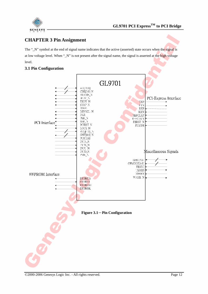
CHAPTER 3 Pin Assignment
The “_N” symbol at the end of signal name indicates that the active (asserted) state occurs when the signal is
at low voltage level. When “_N” is not present after the signal name, the signal is asserted at the high voltage
level.
3.1 Pin Configuration
Figure 3.1-Pin Configuration
GL9701 PCI ExpressTM to PCI Bridge
©2000-2006 Genesys Logic Inc. - All rights reserved. Page 13
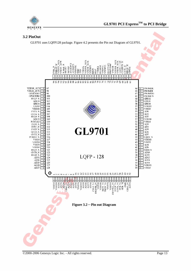
3.2 PinOut GL9701 uses LQFP128 package. Figure 4.2 presents the Pin out Diagram of GL9701.
Figure 3.2-Pin out Diagram
GL9701 PCI ExpressTM to PCI Bridge
©2000-2006 Genesys Logic Inc. - All rights reserved. Page 14
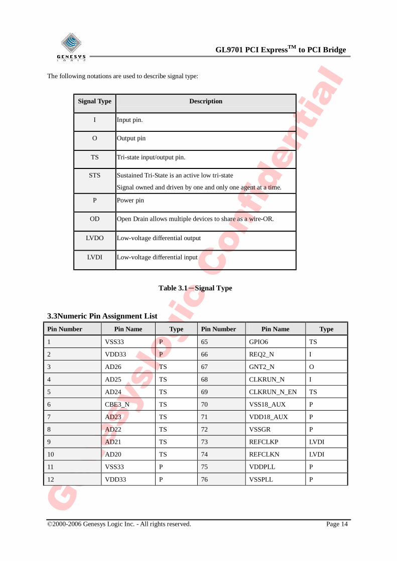
The following notations are used to describe signal type:
Signal Type Description
I Input pin.
O Output pin
TS Tri-state input/output pin.
STS Sustained Tri-State is an active low tri-state
Signal owned and driven by one and only one agent at a time.
P Power pin
OD Open Drain allows multiple devices to share as a wire-OR.
LVDO Low-voltage differential output
LVDI Low-voltage differential input
Table 3.1-Signal Type
3.3Numeric Pin Assignment List Pin Number Pin Name Type Pin Number Pin Name Type
1 VSS33 P 65 GPIO6 TS
2 VDD33 P 66 REQ2_N I
3 AD26 TS 67 GNT2_N O
4 AD25 TS 68 CLKRUN_N I
5 AD24 TS 69 CLKRUN_N_EN TS
6 CBE3_N TS 70 VSS18_AUX P
7 AD23 TS 71 VDD18_AUX P
8 AD22 TS 72 VSSGR P
9 AD21 TS 73 REFCLKP LVDI
10 AD20 TS 74 REFCLKN LVDI
11 VSS33 P 75 VDDPLL P
12 VDD33 P 76 VSSPLL P
GL9701 PCI ExpressTM to PCI Bridge
©2000-2006 Genesys Logic Inc. - All rights reserved. Page 15
13 AD19 TS 77 RTERM I
14 AD18 TS 78 VSSRX P
15 AD17 TS 79 RXP LVDI
16 AD16 TS 80 RXN LVDI
17 CBE2_N TS 81 VDDRX P
18 FRAME_N STS 82 VSS18_AUX P
19 VSS18 P 83 VDD18_AUX P
20 VDD18 P 84 VSSTX P
21 IRDY_N STS 85 TXP LVDO
22 TRDY_N TS 86 TXN LVDO
23 VSS33 P 87 VDDTX P
24 VDD33 P 88 AVSSPCI P
25 DEVSEL_N STS 89 AVDDPCI P
26 STOP_N STS 90 TESTD TS
27 LOCK_N STS 91 TESTC I
28 PER_N TS 92 WAKE_N DO
29 SER_N OD 93 VSS33_AUX P
30 PAR TS 94 VDD33_AUX P
31 CBE1_N TS 95 PERST_N I
32 AD15 TS 96 PME_N I
33 VSS33 P 97 VDD18_AUX P
34 VDD33 P 98 VSS18_AUX P
35 AD14 TS 99 OPMODE1 I
36 AD13 TS 100 OPMODE0 I
37 AD12 TS 101 REQ3_N I
38 AD11 TS 102 GPIO3 TS
39 AD10 TS 103 GPIO4 TS
40 M66EN I 104 VSS33 P
41 AD9 TS 105 VDD33 P
42 AD8 TS 106 INTA_N TS
43 VSS33 P 107 GNT4_N O
44 VDD33 P 108 REQ4_N I
45 CBE0_N TS 109 GPIO5 TS

GL9701 PCI ExpressTM to PCI Bridge
©2000-2006 Genesys Logic Inc. - All rights reserved. Page 16
46 AD7 TS 110 PCICLKI I
47 AD6 TS 111 INTB_N I
48 AD5 TS 112 INTC_N I
49 AD4 TS 113 INTD_N I
50 AD3 TS 114 GNT3_N O
51 VSS18 P 115 GNT1_N O
52 VDD18 P 116 PCIRST_N O
53 AD2 TS 117 VSS18 P
54 AD1 TS 118 VDD18 P
55 AD0 TS 119 VSS33 P
56 VSS33 P 120 VDD33 P
57 VDD33 P 121 REQ1_N I
58 GPIO0 TS 122 GNT0_N O
59 GPIO1 TS 123 REQ0_N I
60 GPIO2 TS 124 AD31 TS
61 PROMCS O 125 AD30 TS
62 PROMDO O 126 AD29 TS
63 PROMDI I 127 AD28 TS
64 PROMSK O 128 AD27 TS
3.4 Signal Description 3.4.1 PCI-Express Interface
Name Type Description
TXP,
TXN
LVDO Transmitter differential pair
RXP,
RXN
LVDI Receiver differential pair
REFCLKP,
REFCLKN
LVDI 100 MHz differential clock input
PERST_N I External reset, low active
RTERM I Connect to a resistor for calibration

GL9701 PCI ExpressTM to PCI Bridge
©2000-2006 Genesys Logic Inc. - All rights reserved. Page 17
3.4.2 Secondary PCI Interface
Name Type Description
AD[31:0] TS Address/Data
CBE[3:0]_N TS Command/Byte Enable
FRAME_N STS Secondary PCI interface frame
IRDY_N STS Secondary PCI interface initiator ready
TRDY_N STS Secondary PCI interface target ready
STOP_N STS Secondary PCI interface stop indicator
DEVSEL_N STS Secondary PCI interface device select
PAR TS Secondary PCI interface parity
PER_N STS Secondary PCI interface parity error detect
SER_N OD Secondary PCI interface system error
PCIRST_N O Secondary PCI bus Reset
LOCK_N STS Secondary PCI interface target ready
REQ[4:0]_N I Requests 4-0, activated by the secondary bus masters to request the
use of the secondary bus.
REQ0_N is a dual-purpose signal. When the bridge’s internal arbiter
is enabled, this signal is used as a request input, to be activated by a
secondary bus master requesting the use of the secondary bus. When
the internal arbiter is disabled, REQ0_N is used by the bridge as its
grant input signal.
GNT[4:0]_N O Grants 4-0, activated by the bridge’s internal arbiter to grant usage of
the secondary bus to the master that activated the corresponding
request signal.
GNT0_N is a dual-purpose signal. When the bridge’s internal arbiter
is enabled, this signal is used as a grant output, activated by the bridge
to grant the use of the secondary bus to the master who requested the
use with the GNT0_N signal. When the internal arbiter is disabled,
this signal is used by the bridge as its request output signal.
PCICLKI I PCI clock input.
INTA_N,
INTB_N,
INTC_N,
I Interrupt from secondary interface.

GL9701 PCI ExpressTM to PCI Bridge
©2000-2006 Genesys Logic Inc. - All rights reserved. Page 18
INTD_N
PME_N I Power management event from secondary interface
WAKE_N OD Used to implement wakeup mechanism.
3.4.3 EEPROM Signals
Name Type Description
PROMCS O Enable EEPROM interface
PROMDO O Serial data output for EEPROM
PROMDI I Serial data input from EEPROM
PROMSK O Serial clock output for EEPROM
3.4.4 Miscellaneous Signals
Name Type Description
GPIO[6:0] TS The output signals are determined by OPMODE[1:0],
PCICLKx_MASK(x=0~5) in design option.
▪For GPIO[2:0]:
Available only in normal mode. (OPMODE[1:0]=2’b00)
▪ If PCICLKx_MASK (x=0~2) are not masked (=1’b0), then
these three bits are used as PCI clock outputs. It’s recommended
that GPIO[0] be routed to PCICLKI input.
▪ If PCICLKx_MASK (x=0~2) are masked (=1’b1) then these
three bits are used as output of GPIO signal from design option.
▪For GPIO[5:3]:
▪ If in normal function mode (OPMODE[1:0]=2’b00), then these
three bits are used as PCI clock outputs when
PCICLKx_MASK(x=5~3) are not masked (=1’b0). These three
bits are used as GPIO output from design option if
PCICLKx_MASK(x=5~3) are masked (=1’b1).
▪ If in test mode (OPMODE[1:0]=2’b01), then these three bits are
used as internal signal output.
▪For GPIO[6]:
▪ If in normal function mode (OPMODE[1:0]=2’b00), the bit is
used as GPIO pins. Users can specify the output value and
GL9701 PCI ExpressTM to PCI Bridge
©2000-2006 Genesys Logic Inc. - All rights reserved. Page 19
output enable via design option. Users can also probe the input
value by reading the design option.
▪ If in normal function (OPMODE[1:0]=2’b01), then this bit is
used as internal signal output.
OPMODE[1:0] I Operation mode setup
TESTC I Test clock
TESTD TS Test data
CLKRUN_N TS A PCI device can request GL9701 to start, speed up, or maintain the
PCI clock by the assertion of CLKRUN_N. GL9701 is responsible
for maintaining CLKRUN_N asserted, and for driving it high to the
de-asserted state.
CLKRUN_N_E
N
I Clock Run Enable
1’b1: Enable Clock Run
1’b0: Disable Clock Run
M66EN I Enable PCI clock act as 33MHz or 66MHz.
1: PCI Clocks are 66MHz.
0: PCI clocks are 33MHz
3.4.5 Power and Ground Signals
Name Type Description
VSS33 P Ground for PCI PAD
VDD33 P 3.3V Power Supplier for PCI PAD
VSS18_AUX P Ground for 1.8 Vaux
VDD18_AUX P 1.8Vaux Power Supplies for core voltage
VSS33_AUX P Ground for 3.3 Vaux
VDD33_AUX P 3.3Vaux Power Supplies for core voltage
VSS18 P Digital ground
VDD18 P 1.8V Power Supplies for core voltage
VSSGR P Ground for the guard ring of the SerDes block
VDDPLL P 1.8V Power Supplies for internal PLL
VSSPLL P Ground for internal PLL
VSSRX
VDDRX
P 1.8V Power Supplies for receiver part
GL9701 PCI ExpressTM to PCI Bridge
©2000-2006 Genesys Logic Inc. - All rights reserved. Page 20
VSSTX
VDDTX
P 1.8V Power Supplies for transceiver part
AVSSPCI
AVDDPCI
P 1.8V Power Supplier for PCI PLL
GL9701 PCI ExpressTM to PCI Bridge
©2000-2006 Genesys Logic Inc. - All rights reserved. Page 21
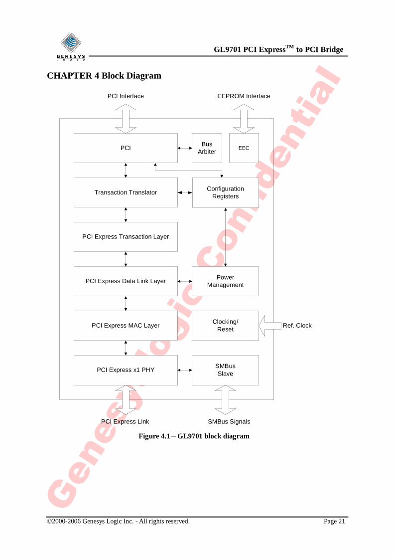
CHAPTER 4 Block Diagram
PCI
PCI Express Transaction Layer
PCI Express Data Link Layer
PCI Express MAC Layer
PCI Express x1 PHY
PCI Express Link
PCI Interface
PowerManagement
Clocking/Reset
BusArbiter
SMBusSlave
Ref. Clock
SMBus Signals
Transaction Translator
EEC
EEPROM Interface
ConfigurationRegisters
Figure 4.1-GL9701 block diagram

GL9701 PCI ExpressTM to PCI Bridge
©2000-2006 Genesys Logic Inc. - All rights reserved. Page 22
The GL9701 is composed of the following major functional blocks as shown in Figure 3-1:
• PCI interface macro
The macro acts as either a bus master or a bus slave and handles the PCI protocol depending on the
transaction types. GL9701 supports 32-bit PCI addressing with 0MHz~33MHz and 66MHz operation
frequency.
Table3.1 summarizes the PCI commands supported by GL9701
Command Type Encoding
I/O Read 0010
I/O Write 0011
Memory Read 0110
Memory Write 0111
Configuration Read 1010
Configuration Write 1011
Memory Read Multiple 1100
Memory Read Line 1110
Memory Write and
Invalidate
1111
Table 4.1-Supported PCI Command
• Bus Arbiter
This block supports PCI bus arbiter for secondary PCI bus. The bus arbitration is provided by GL9701
and supports up to five external masters. The arbiter can be disabled by external EEPROM.
• Configuration Registers
This module supports two mechanisms for configuration space access: PCI compatible and PCI Express
enhanced configuration mechanism.
• Power Management
The moudle is in charge of power management event signaling. This module enables GL9701 to enter
software driven D-state transitions.
• Transaction Translator
The Transaction Translator manages all the bridge operation between PCI Express and PCI interface. It
is responsible for PCI Express to PCI command translation, message translation and managing
transaction ordering.

GL9701 PCI ExpressTM to PCI Bridge
©2000-2006 Genesys Logic Inc. - All rights reserved. Page 23
• PCI Express Transaction Layer
The layer’s function is the assembly and disassembly of Transaction Layer Packets (TLPs). It is also
responsible for managing credit-based flow control for TLPs.
• PCI Express Data Link Layer
The layer serves as an intermediate stage between the Transaction Layer and the Physical Layer. The
responsibility is Link management and data integrity including error detection and error correction.
• PCI Express MAC Layer
The Layer can be taken as a part of Physical Layer. It includes link initialization, link state management,
lane alignment, data scrambling and descrambling.
• PCI Express x1 PHY
The PHY includes all circuitry for interface operation for an x1 link, including driver and input buffers,
parallel-to-serial and serial-to-parallel conversion, PLL(s) and impedance matching circuitry. It also
includes logical function related to 8b/10b encoding/decoding and PHY status report.
• SMBus Slave
The SMBus Slave handles SMBus protocol and provides the access to internal registers such as chip
information, function options and some test setting.
• EEC, EERPOM Controller
Provide a download path for chip configuration and information.
• Clocking/Reset
Provide a clocking and reset to manage all blocks.

GL9701 PCI ExpressTM to PCI Bridge
©2000-2006 Genesys Logic Inc. - All rights reserved. Page 24
CHAPTER 5 Function Description 5.1 Power Management
GL9701 supports PCI-PM 1.1 Compatible Power Management and Active State Power Management (ASPM)
defined in PCI Express Base Specification Revision 1.0a.
5.1.1 PCI-PM Software Compatible Power Management
GL9701 supports link states L0, L1 and L2 needed to implement PCI-PM compatible power states D0, D1, D2
and D3hot. All link states are determined by the D-state of the bridge. Because GL9711 provides Vaux, bridge
will enter into L2 state when software direct bridge into D3hot state. Refer to the PCI Express Base
Specification Revision 1.0a for more protocol information involved in transitioning the link to the L1 or L2
state.
5.1.2 Hardware-Controlled Active State Power Management
GL9701 supports a hardware-initiated power management mechanism which is called Active State Power
Management (ASPM). Once this feature is enabled, bridge will drive the link state into a low-power L0s link
state or even lower-power L1 link state. Refer to the PCI Express Base Specification Revision 1.0a for more
information about ASPM.
Once system software enables GL9701’s ASPM capability by setting the ASPM Control bit of Link Control
Register to high, GL9701 will behavior ASPM specified in PCI Express Base Specification Revision 1.0a by
default. However, GL9701 can disable this mechanism via the optional setting specified in table6.1. The
optional bit is the 30th bit of Configuration Space Register with offset ‘hc8. If this bit is set to low, then
GL9701 will never act ASPM behavior no matter what value of the ASPM Control bit of Link Control
Register.
5.1.3 In-band Beacon
Beacon is a in-band signal used to exit the L2 link power management state and informs the Root Complex to
re-activate the link. When the bridge is directed into D3hot State, the link state will finally stay in L2 State.
The device on the secondary PCI bus wakes up the system by asserting PME_N. GL9701 then outputs the
beacon signal on the upstream PCI Express link. Root complex should re-apply the power and reference
clock again after detecting the beacon.

GL9701 PCI ExpressTM to PCI Bridge
©2000-2006 Genesys Logic Inc. - All rights reserved. Page 25
5.1.4 Side-band WAKE_N
GL9701 supports two means to signal the platform to re-establish the power and reference clock while the
bridge is placed into D3hot state. One is Beacon, and the other is WAKE_N. WAKE_N.
WAKE_N is a side-band signal and is low active. Similar with Beacon, the bridge only outputs WAKE_N
when the bridge detects PME_N asserted by the device on the secondary PCI bus when the bridge is placed
into D3hot state.
5.1.5 Power Management System Messages GL9701 supports all messages involved in the Power Management. GL9701 either initiates or receives them.
Table5-1 outlines their characteristics.
Packet Type
PM_Enter_L1 DLLP
PM_Enter_L23 DLLP
PM_Active_State_Request_L1 DLLP
PM_Request_Ack DLLP
PM_Active_State_Nak TLP
PM_PME TLP
PME_Turn_Off TLP
PME_TO_Ack TLP
5.2 PCI Clock Run GL9701 supports Clock Run functionality specified in PCI Mobile Design Guide v1.1. CLKRUN_N is an
optional signal used by devices to request starting (or speeding up) the clock. A device requests the central
resource to start, speed up, or maintain the PCI clock by the assertion of CLKRUN_N. The central resource is
responsible for maintaining CLKRUN_N asserted, and for driving it high to the de-asserted state.
Clock Run functionality in GL9701 can be enabled by the asserting CLKRUN_N_EN (PIN69) to high. When
the function is enabled, GL9701 plays the role of central resource. There is a ODT inside the CLKRUN_N
(PIN68), so there is no need to add an external pull up resistor on the CLKRUN_N.
5.3 PCI Clock GL9701 supports five PCI slots on the secondary PCI interface. To provide the devices on these slots and
GL9701 itself can work properly, GL9701 provides six PCI clock sources.
GL9701 PCI ExpressTM to PCI Bridge
©2000-2006 Genesys Logic Inc. - All rights reserved. Page 26
The operational frequency of these PCI clocks can be configured by M66EN (PIN40). When it’s set to high,
then the PCI clocks will operate at 66MHz. When it’s set to low, then these clocks will operate at 33MHz.
The six clock output are at GLIO0 ~ GPIO5. It’s recommended that GPIO0 be connected to PCICLKI
(PIN110) to feed GL9701 itself. GPIO1 ~ GPIO5 then can be distributed to the five PCI slots. Users may
optionally implement the number of PCI slots greater than one and less than five. Users can even use an
external PCI clock source to maintain the normal operation of GL9701 and its secondary PCI slots.
If not all the five PCI slots are utilized, users can use the GPIOx (x=1~5, 0 is valid when an external PCI clock
source is provided) for the use of General Purpose I/O. The optional use between PCI clock source and GPIO
can be determined by the PCICLK_MASKx (x=0~5).
When PCICLK_MASKx (x=0~5) is set, the PCI clock output of the corresponding GPIOx is masked. The
GPIOx then becomes a General Purpose I/O. Users then can arbitrarily specify the output enable control
(GPIOx_OE) and the output value (GPIOxO) for the GPIOx.
GL9701 also provides a General Purpose I/O , GPIO6 (PIN65), for users to use. Unlike GPIO0~GPIO5, this
pin does not Mux other functions. Users just have to control the output enable (GPIO6_OE) and its output
value (GPIO6O).
5.4 Interrupt mapping PCI INTx interrupts are “virtualized” in PCI Express using Assert_INTx and Deassert_INTx
messages, where x is A, B, C, and D for the respective PCI INTx# interrupt signals defined in
PCI 3.0. This message pairing provides a mechanism to preserve the level-sensitive semantics of the PCI
interrupts. The Assert_INTx and Deassert_INTx messages transmitted on the PCI Express Link capture the
asserting/deasserting edge of the respective PCI INTx# signal.
GL9701 is a multi-ported PCI Express bridge. A multi-ported PCI Express bridges must collapse the
INTA#-INTD# pins from each of their downstream conventional PCI interface into four INTx “virtual wires” on
their Upstream Port. The mapping between the INTx# pin on a PCI bus and the corresponding INTx messages
on the PCI Express Link is based on the device number of the PCI bridge assigned to the port requesting the
interrupt. The mapping is as follows:

GL9701 PCI ExpressTM to PCI Bridge
©2000-2006 Genesys Logic Inc. - All rights reserved. Page 27
Device Number of
Conventional GL9701
Supporting
Secondary Interface
(Interrupt Source)
INTx# Interrupt Line from
Downstream
Conventional PCI
Interface
Mapping to INTx Virtual
Wire on Primary Side of
Bridge
INTA# INTA
INTB# INTB
INTC# INTC 0, 4
INTD# INTD
INTA# INTB
INTB# INTC
INTC# INTD 1
INTD# INTA
INTA# INTC
INTB# INTD
INTC# INTA 2
INTD# INTB
INTA# INTD
INTB# INTA
INTC# INTB 3
INTD# INTC
5.5 Initial Flow Control Advertisements
Flow control value for various credit type is advertised after the link is established. The initial value for each
credit type in GL9701 is as followed:
Credit Type Initial Flow Control Value
Posted Request headers (PH) 04h
Posted Request Data payload (PD) 20h
Non-Posted Request headers (NPH) 04h
Non-Posted Request Data payload (NPD) 04h
Completion headers (CPLH) 08h
Completion Data payload (CPLD) 20h

GL9701 PCI ExpressTM to PCI Bridge
©2000-2006 Genesys Logic Inc. - All rights reserved. Page 28
5.6 IDSEL Mapping
While receiving a Type1 Configuration Cycle from the upstream PCI Express port, GL9701 will convert it
into a Type0 Configuration Cycle if the bus number is within the range specified by the Primary Bus Number
Register and the Secondary Bus Number Register.
The format of a Type0 Configuration Cycle is as followed:
GL9701 converts the destination ID device number to one of the AD[31:16] as the IDSEL of the five PCI slots.
The mapping between the AD[31:16] and Device Number is:
Device Number [4:0] AD[31:16]
00000 0000_0000_0000_0001
00001 0000_0000_0000_0010
00010 0000_0000_0000_0100
00011 0000_0000_0000_1000
00100 0000_0000_0001_0000
00101 0000_0000_0010_0000

GL9701 PCI ExpressTM to PCI Bridge
©2000-2006 Genesys Logic Inc. - All rights reserved. Page 29
CHAPTER 6 Register Description GL9701 implements the standard PCI Express-to-PCI Bridge configuration space format. Figure5.1 shows the
capabilities supported by GL9701. Table5.1 and Table5.2 represent the configuration registers of GL9701 and
their address byte offset values.
Configuration register fields are assigned one of the attributes described in Table5.1.
Register Attribute Description
HwInit Hardware Initialized: Register bits are initialized by
firmware or hardware mechanisms such as pin strapping or
serial EEPROM. Bits are read-only after initialization and can
only be reset (for write-once by firmware) with Fundamental
Reset.
RO Read-only register: Register bits are read-only and cannot be
altered by software. Register bits may be initialized by
hardware mechanisms such as pin strapping or serial
EEPROM.
RW Read-Write register: Register bits are read-write and may be
either set or cleared by software to the desired state.
RW1C Read-only status, Write-1-to-clear status register: Register
bits indicate status when read, a set bit indicating a status
event may be cleared by writing a 1. Writing a 0 to RW1C
bits has no effect.
ROS Sticky – Read-only register: Registers are read-only and
cannot be altered by software. Registers are not initialized or
modified by hot reset.
RWS Sticky – Read-Write register: Registers are read-write and
may be either set or cleared by software to the desired state.
Bits are not initialized or modified by hot reset.
RW1CS Sticky – Read-only status, Write-1-to-clear status register:
Registers indicate status when read, a set bit indicating a
status event may be cleared by writing a 1. Writing a 0 to
RW1CS bits has no effect. Bits are not initialized or modified
by hot reset.
RsvdP Reserved and Preserved: Reserved for future RW

GL9701 PCI ExpressTM to PCI Bridge
©2000-2006 Genesys Logic Inc. - All rights reserved. Page 30
implementations; software must preserve value read for
writes to bits.
RsvdZ Reserved and Zero: Reserved for future RW1C
implementations; software must use 0 for writes to bits.
Table 6.1-Notation for attribute

GL9701 PCI ExpressTM to PCI Bridge
©2000-2006 Genesys Logic Inc. - All rights reserved. Page 31
0x00
0x3c
0x6c
0x70
0x80
0x40
0x94
0x98
0x84
0x90
0x9c
0xfc
0x100
0x158
0x148
0x150
Figure 6.1-GL9701 Capabilities

GL9701 PCI ExpressTM to PCI Bridge
©2000-2006 Genesys Logic Inc. - All rights reserved. Page 32
Byte Offset
Bit31 0
Device ID Vendor ID 00h
Status Command 04h
Class Code Revision ID 08h
BIST
Header Type Primary
Latency Timer
Cache Line Size
0Ch
Base Address Register 0 10h
Base Address Register 1 14h
Secondary
Latency timer
Subordinate
Bus Number
Secondary Bus
Number
Primary Bus
Number
18h
Secondary Status I/O Limit I/O Base 1Ch
Memory Limit Memory Base 20h
Prefetchable Memory Limit Prefetchable Memory Base 24h
Prefetchable Base Upper 32 Bits 28h
Prefetchable Limit Upper 32 Bits 2Ch
I/O Limit Upper 16 Bits I/O Base Upper 16 Bits 30h
Reserved Capabilities Pointer 34h
Expansion ROM Base Address 38h
Type1 Header
Bridge Control Interrupt Pin Interrupt Line 3Ch
PCI Express Capabilities
Register
Next Cap Pointer
PCI Express
Cap ID
70h
Device Capabilities 74h
Device Status Device Control 78h
Link Capabilities 7Ch
Link Status Link Control 80h
Reserved 84h
Reserved Reserved 88h
Reserved Reserved 8Ch
PCI Express
Capability
Reserved 90h

GL9701 PCI ExpressTM to PCI Bridge
©2000-2006 Genesys Logic Inc. - All rights reserved. Page 33
Power Management Capability
register
Next Pointer(43h) PM Capability ID 94h Power
Management
Capability Data PM Ctrl/Stat
Bridge Ext
Power Management Status and
Control
98h
Table 6.2-Legacy Configuration Space
PCI Express Extended Capabilities Space
Advanced Error Reporting
Capability Header
Next Cap Pointer PCI Express
Extended
Capability ID
100h
Uncorrectable Error Status Register 104h
Uncorrectable Error Mask Register 108h
Uncorrectable Error Severity Register 10Ch
Correctable Error Status Register 110h
Correctable Error Mask Register 114h
Advanced Error Capabilities and Control Register 118h
11Ch
120h
124h
Header Log Register
128h
Root Error Command –Not Implemented 12Ch
Root Error Status –Not Implemented 130h
Advanced
Error
Reporting
Capability
Error Source ID Register –Not Implemented
Correctable Error
Source ID
Register – Not
Implemented
134h
PCI Express Enhanced Capability Header 150h
Serial Number Register (Lower DW) 154h
Device Serial
Number
Capability Serial Number Register (Upper DW) 158h
Table 6.3-PCI Express Extended Configuration Space

GL9701 PCI ExpressTM to PCI Bridge
©2000-2006 Genesys Logic Inc. - All rights reserved. Page 34
6.1 Offset 00h: Device Identification
Generic configuration software will be able to determine what devices are available on PCI bus via these
information. All of these registers are read-only.
Bits Type Default Description
15:0 RO 17a0h Vendor ID: This field identifies the manufacturer of the device.
31:16 RO 7163 Device ID: This field identifies the particular device.
6.2 Offset 04h: Command Register
Bits Type Default Description
0 RW 0b
I/O Space: Controls a device’s response to I/O Space accesses.
0– Disables the device response.
1– Allows the device torespond to I/O Space accesses.
1 RW 0b
Memory Space: Controls a device’s response to Memory Space
accesses.
0– Disables the device response.
1– Allows the device to respond to Memory Space accesses.
2 RW 0b
Bus Master: Controls a device’s ability to act as a master on the
PCI bus.
0– Disables the device from generating PCI accesses.
1– Allows the device to behave as a bus master.
3 RO 0b Special Cycles: Does not apply to PCI Express Bridge.
4 RO 0b
Memory Write and Invalidate Enable: GL9701 does not
optionally promote Memory Write Requests to Memory Write
and Invalidate transactions on PCI.
5 RO 0b VGA Palette Snoop: Does not apply to PCI Express bridges.
6 RW 0b
Parity Error Response:
Controls the bridge’s setting of the Master Data Parity Error bit in
the Status register in response to a received poisoned TLP from
PCI Express.
0 – Disables the setting of the Master Data Parity Error bit.

GL9701 PCI ExpressTM to PCI Bridge
©2000-2006 Genesys Logic Inc. - All rights reserved. Page 35
1– Enables the setting of the Master Data Parity Error bit.
7 RO 0b Reserved
8 RW 0b
SERR# Enable: This bit enables reporting of non-fatal and
fatal errors to the Root Complex. In addition, this bit enables
transmission by the primary interface of ERR_NONFATAL and
ERR_FATAL error messages on behalf of SERR# assertions
detected on the secondary interface. Note that errors are reported if
enabled either through this bit or through the PCI Express specific
bits in the Device Control register.
0 – Disable the reporting of bridge non-fatal errors and
fatal errors to the Root Complex.
1 – Enable the reporting of bridge non-fatal errors and fatal
errors to the Root Complex.
9 RO 0b Fast Back-to-Back Transactions Enable: Does not apply to PCI
Express bridges.
10 RW 0b Interrupt Disable: GL9701 does not generate INTx interrupt
messages on behalf of internal sources hence implements this bit as
read-only with a value of 0.
15:11 RO 00h Reserved
6.3 Offset 06h: Status Register
Bits Type Default Description
2:0 RO 0h Reserved
3 RO 0b Interrupt Status – Indicates that an INTx interrupt message is
pending on behalf of sources internal to the bridge.
4 RO 1b Capabilities List – Indicates the presence of a Capability List
item.
5 RO 0b 66 MHz Capable – Does not apply to PCI Express bridges.
6 RO 0b Reserved
7 RO 0b Fast Back-to-Back Transactions Capable – Does not apply to
PCI Express bridges.

GL9701 PCI ExpressTM to PCI Bridge
©2000-2006 Genesys Logic Inc. - All rights reserved. Page 36
8 RW1C 0b
Master Data Parity Error – This bit is used to report the
detection of uncorrectable data errors by the bridge. This bit is set
if the Parity Error Response bit in the Command register is set and
either of the following two conditions occur:
The bridge receives a Completion with data marked
poisoned on the primary interface.
The bridge poisons a write Request on the primary interface.
0 – No uncorrectable data error detected on the primary
interface.
1– Uncorrectable data error detected on the primary
interface.
10:9 RO 00b DEVSEL# Timing – Does not apply to PCI Express bridges.
Must be hardwired to 00b.
11 RW1C 0b
Signaled Target-Abort – This bit is set when the bridge
generates a completion with Completer Abort Completion Status in
response to a request received on its primary interface.
0 – Completer Abort Completion not transmitted on the
primary interface.
1 – Completer Abort Completion transmitted on the primary
interface.
12 RW1C 0b
Received Target-Abort – This bit is set when the bridge
receives a Completion with Completer Abort Completion Status on
its primary interface.
0 – Completer Abort Completion Status not received on
primary interface.
1 – Completer Abort Completion Status received on primary
interface.
13 RW1C 0b
Received Master-Abort – This bit is set when the bridge
receives a Completion with Unsupported Request Completion
Status on its primary interface.
0 – Unsupported Request Completion Status not received on
primary interface.
1 – Unsupported Request Completion Status received on
primary interface.
GL9701 PCI ExpressTM to PCI Bridge
©2000-2006 Genesys Logic Inc. - All rights reserved. Page 37
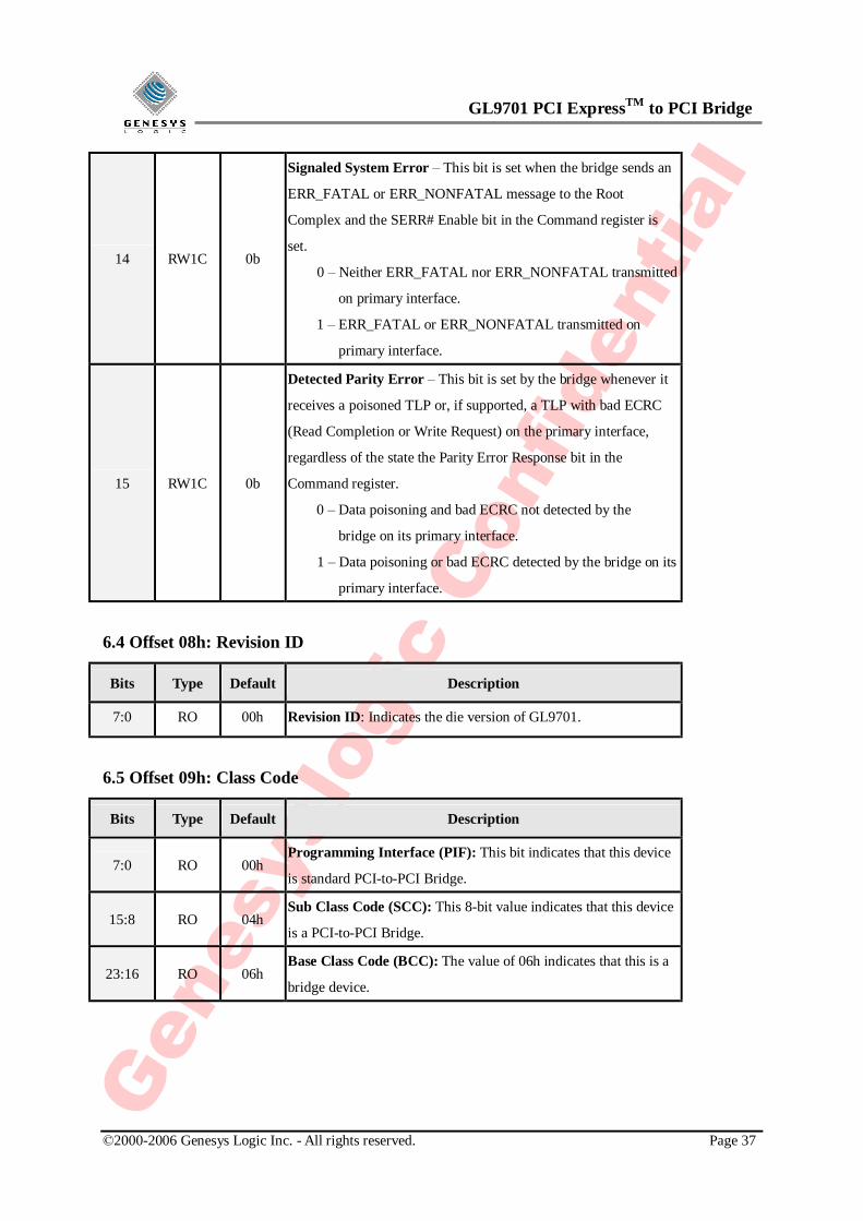
14 RW1C 0b
Signaled System Error – This bit is set when the bridge sends an
ERR_FATAL or ERR_NONFATAL message to the Root
Complex and the SERR# Enable bit in the Command register is
set.
0 – Neither ERR_FATAL nor ERR_NONFATAL transmitted
on primary interface.
1 – ERR_FATAL or ERR_NONFATAL transmitted on
primary interface.
15 RW1C 0b
Detected Parity Error – This bit is set by the bridge whenever it
receives a poisoned TLP or, if supported, a TLP with bad ECRC
(Read Completion or Write Request) on the primary interface,
regardless of the state the Parity Error Response bit in the
Command register.
0 – Data poisoning and bad ECRC not detected by the
bridge on its primary interface.
1 – Data poisoning or bad ECRC detected by the bridge on its
primary interface.
6.4 Offset 08h: Revision ID
Bits Type Default Description
7:0 RO 00h Revision ID: Indicates the die version of GL9701.
6.5 Offset 09h: Class Code
Bits Type Default Description
7:0 RO 00h Programming Interface (PIF): This bit indicates that this device
is standard PCI-to-PCI Bridge.
15:8 RO 04h Sub Class Code (SCC): This 8-bit value indicates that this device
is a PCI-to-PCI Bridge.
23:16 RO 06h Base Class Code (BCC): The value of 06h indicates that this is a
bridge device.

GL9701 PCI ExpressTM to PCI Bridge
©2000-2006 Genesys Logic Inc. - All rights reserved. Page 38
6.6 Offset 0ch: Cache Line Size Register
Bits Type Default Description
7:0 RW 00h Cache Line Size: Specifies the system cacheline size in units of
DWORDs.
6.7 Offset 0dh: Primary Latency Timer Register
Bits Type Default Description
7:0 RO 00h Primary Latency Timer: The primary/master latency timer does
not apply to PCI Express bridges..
6.8 Offset 0eh: Header Type Register
Bits Type Default Description
7:0 RO 01h Header Type: Indicates that the header is compatible with PCI
system software developed for Type 01h PCI and PCI-X bridges.
6.9 Offset 0fh: Bist Register
Bits Type Default Description
7:0 RO 00h BIST: GL9701 does not support BIST.
6.10 Offset 10h: Base Register0
Bits Type Default Description
31:0 RO 00h Base Register0: GL9701 does not use base register.
6.11 Offset 14h: Base Register1
Bits Type Default Description
31:0 RO 00h Base Register1: GL9701 does not use base register.
GL9701 PCI ExpressTM to PCI Bridge
©2000-2006 Genesys Logic Inc. - All rights reserved. Page 39
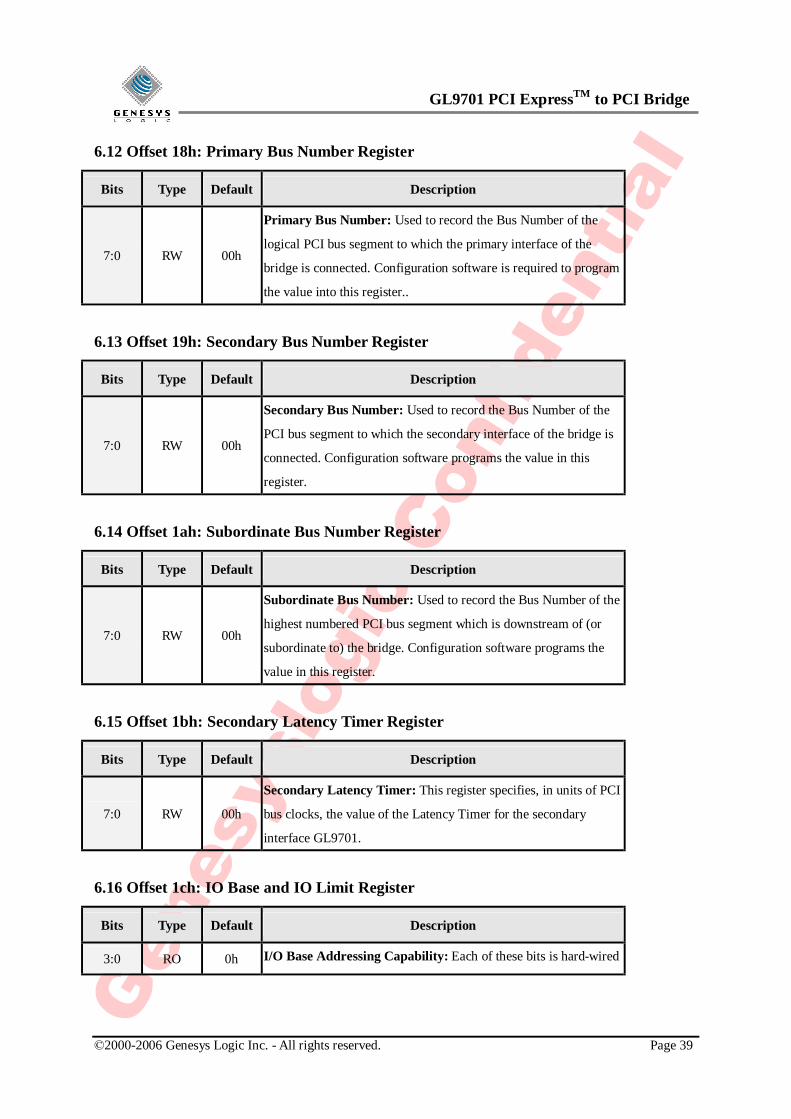
6.12 Offset 18h: Primary Bus Number Register
Bits Type Default Description
7:0 RW 00h
Primary Bus Number: Used to record the Bus Number of the
logical PCI bus segment to which the primary interface of the
bridge is connected. Configuration software is required to program
the value into this register..
6.13 Offset 19h: Secondary Bus Number Register
Bits Type Default Description
7:0 RW 00h
Secondary Bus Number: Used to record the Bus Number of the
PCI bus segment to which the secondary interface of the bridge is
connected. Configuration software programs the value in this
register.
6.14 Offset 1ah: Subordinate Bus Number Register
Bits Type Default Description
7:0 RW 00h
Subordinate Bus Number: Used to record the Bus Number of the
highest numbered PCI bus segment which is downstream of (or
subordinate to) the bridge. Configuration software programs the
value in this register.
6.15 Offset 1bh: Secondary Latency Timer Register
Bits Type Default Description
7:0 RW 00h
Secondary Latency Timer: This register specifies, in units of PCI
bus clocks, the value of the Latency Timer for the secondary
interface GL9701.
6.16 Offset 1ch: IO Base and IO Limit Register
Bits Type Default Description
3:0 RO 0h I/O Base Addressing Capability: Each of these bits is hard-wired

GL9701 PCI ExpressTM to PCI Bridge
©2000-2006 Genesys Logic Inc. - All rights reserved. Page 40
to 0, indicating support for 16-bit I/O addressing only.
7:4 RW 0h
I/O Base Address Bits [15:12]: These bits define the bottom
address of an address range to determine when to forward I/O
transactions from one interface to another.
These bits correspond to address lines[15:12] for 4 KB alignment.
Bits[11:0] are assumed to be 000h.
11:8 RO 0h I/O Limit Addressing Capability (IOLC): Each of these bits is
hard-wired to 0, indicating support for 16-bit I/O addressing only.
15:12 RW 0h
I/O Limit Address Bits [15:12] (IOLA): These bits define the top
address of an address range to determine when to forward I/O
transactions from PCI Express* to PCI. These bits correspond to
address lines[15:12] for 4 KB aligned window. Bits[11:0] are
assumed to be FFFh.
6.17 Offset 1eh: Secondary Status Register
Bits Type Default Description
4:0 RsvdZ 00h Reserved
5 RO 1b 66 MHz Capable: This bit indicates that the secondary interface
of the bridge is 66 MHz-capable.
6 RsvdZ 0b Reserved
7 RO 0b
Fast Back-to-Back Transactions Capable: This bit indicates that
the secondary interface is not able to receive fast back-to-back
cycles.
8 RW1C 0b
Master Data Parity Error – This bit is used to report the
detection of an uncorrectable data error by the bridge. This bit is
set if the bridge is the bus master of the transaction on the
secondary interface, the Parity Error Response Enable bit in the
Bridge Control register is set, and either of the following two
conditions occur:
The bridge asserts PERR# on a read transaction.
The bridge detects PERR# asserted on a write transaction.
Once set, this bit remains set until it is reset by writing a 1 to this

GL9701 PCI ExpressTM to PCI Bridge
©2000-2006 Genesys Logic Inc. - All rights reserved. Page 41
bit location. If the Parity Error Response Enable bit is set to zero,
this bit will not be set when an error is detected.
0 – No uncorrectable data error detected on the secondary
interface.
1 – Uncorrectable data error detected on the secondary
interface.
10:9 RO 01b
DEVSEL Timing – This bit field encodes the timing of the
secondary interface DEVSEL# as listed below.
00 – Fast DEVSEL# decoding
01 – Medium DEVSEL# decoding
10 – Slow DEVSEL# decoding
11 – Reserved
11 RW1C 0b
Signaled Target-Abort – This bit reports the signaling of a
Target-Abort termination by the bridge when it responds as the
target of a transaction on its secondary interface or when it signals
a PCI-X Split Completion with Target-Abort.
0 – Target-Abort not signaled on secondary interface.
1 – Target-Abort signaled on secondary interface.
12 RW1C 0b
Received Target-Abort – This bit reports the detection of a
Target-Abort termination by the bridge when it is the master of a
transaction on its secondary interface.
0 – Target-Abort not detected on secondary interface.
1 – Target-Abort detected on secondary interface.
13 RW1C 0b
Received Master-Abort – This bit reports the detection of a
Master-Abort termination by the bridge when it is the master of a
transaction on its secondary interface.
0 – Master-Abort not detected on secondary interface.
1 – Master-Abort detected on secondary interface.
14 RW1C 0b
Received System Error – This bit reports the detection of an
SERR# assertion on the secondary interface of the bridge.
0 – SERR# assertion on the secondary interface has not
been detected.
1 – SERR# assertion on the secondary interface has been
detected.

GL9701 PCI ExpressTM to PCI Bridge
©2000-2006 Genesys Logic Inc. - All rights reserved. Page 42
15 RW1C 0b
Detected Parity Error – This bit reports the detection of an
uncorrectable address, attribute, or data error by the bridge on its
secondary interface.
The bit is set irrespective of the state of the Parity Error
Response Enable bit in the Bridge Control register.
0 – Uncorrectable address, attribute, or data error not
detected on secondary interface
1 – Uncorrectable address, attribute, or data error detected on
secondary interface
6.18 Offset 20h: Memory Base and Limit Register
Bits Type Default Description
3:0 RO 0h Reserved
15:4 RW 000h
Memory Base: These bits are compared with bits[31:20] of the
incoming address to determine the lower 1 MB-aligned value
(inclusive) of the range. The incoming address must be greater
than or equal to this value.
19:16 RO 0h Reserved
31:20 RW 000h
Memory Limit: These bits are compared with bits[31:20] of the
incoming address to determine the upper 1 MB-aligned value
(exclusive) of the range. The incoming address must be less than
this value.
6.19 Offset 24h: Prefetchable Memory Base and Limit Register
Bits Type Default Description
3:0 RO 0h 64-bit Indicator: These bits indicate that 64-bit addressing is not
supported for the base.
15:4 RW 000h
Prefetchable Memory Base: These bits are compared with
bits[31:20] of the incoming address to determine the lower 1
MB-aligned value (inclusive) of the range. The incoming address
must be greater than or equal to this value.

GL9701 PCI ExpressTM to PCI Bridge
©2000-2006 Genesys Logic Inc. - All rights reserved. Page 43
19:16 RO 0b 64-bit Indicator: These bits indicate that 64-bit addressing is not
supported for the limit.
31:20 RW 000h
Prefetchable Memory Limit: These bits are compared with
bits[31:20] of the incoming address to determine the upper 1
MB-aligned value (inclusive) of the range. The incoming address
must be less than this value.
6.20 Offset 28h: Prefetchable Base Upper 32-bits Register
Bits Type Default Description
31:0 RO 0000-0000h Prefetchable Memory Base Upper 32bit: These bits indicate that
full 64-bit addressing is not supported.
6.21 Offset 2ch: Prefetchable Limit Upper 32-bits Register
Bits Type Default Description
31:0 RO 0000-0000h Prefetchable Memory Limit Upper 32bit: These bits indicate
that full 64-bit addressing is not supported.
6.22 Offset 30h: IO Base and Limit Upper 16-bits Register
Bits Type Default Description
15:0 RO 0000h I/O Base Upper 16 Bits: 32-bit IO addressing is not supported
31:16 RO 0000h I/O Limit Upper 16 Bits: 32-bit IO addressing is not supported
6.23 Offset 34h: Capabilities Pointer Register
Bits Type Default Description
7:0 RO 70h
Capabilities Pointer: These bits indicate that the pointer for the
first entry in the capabilities list is at 70h in the configuration
space.

GL9701 PCI ExpressTM to PCI Bridge
©2000-2006 Genesys Logic Inc. - All rights reserved. Page 44
6.24 Offset 3ch: Interrupt Line Register
Bits Type Default Description
7:0 RW 00h
Interrupt Line: Used to communicate interrupt line routing
information. Software will write the routing information into this
register as it initializes and configures the system.
6.25 Offset 3dh: Interrupt Pin Register
Bits Type Default Description
7:0 RO 00h Interrupt Pin: GL9701 does not use an interrupt pin.
6.26 Offset 3eh: Bridge Control Register
Bits Type Default Description
0 RW 0b
Parity Error Response Enable – Controls the bridge’s
response to uncorrectable address, attribute, and data errors on the
secondary interface.
0 – Ignore uncorrectable address, attribute, and data
errors on the secondary interface.
1 – Enable uncorrectable address, attribute, and data error
detection and reporting on the secondary interface.
1 RW 0b
SERR# Enable – Controls the forwarding of secondary interface
SERR# assertions to the primary interface. The bridge will
transmit an ERR_FATAL or ERR_NONFATAL cycle on the
primary interface when all of the following are true:
SERR# is asserted on the secondary interface .
This bit is set or Advanced Error Reporting is supported and the
SERR# Assertion Detected Mask bit is clear in the
Secondary Uncorrectable Error Mask register.
The SERR# Enable bit is set in the Command register or the PCI
Express-specific bits are set (refer to Chapter 10 for
details) in the Device Control register of the PCI Express
Capability Structure.

GL9701 PCI ExpressTM to PCI Bridge
©2000-2006 Genesys Logic Inc. - All rights reserved. Page 45
0 – Disable the forwarding of SERR# from the secondary
interface to ERR_FATAL and ERR_NONFATAL
1– Enable the forwarding of secondary SERR# to
ERR_FATAL or ERR_NONFATAL.
2 RW 0b
ISA Enable – Modifies the response by the bridge to ISA I/O
addresses. This applies only to I/O addresses that are enabled by
the I/O Base and I/O Limit registers and are in the first 64 KB of
PCI I/O address space (0000 0000h to 0000 FFFFh). If this bit is
set, the bridge will block any forwarding from primary to
secondary of I/O transactions addressing the last 768 bytes in each
1-KB block. In the opposite direction (secondary to primary), I/O
transactions will be forwarded if they address the last 768 bytes in
each 1-KB block.
0 – Forward downstream all I/O addresses in the address
range defined by the I/O Base and I/O Limit registers.
1– Forward upstream ISA I/O addresses in the address
range defined by the I/O Base and I/O Limit registers that
are in the first 64 KB of PCI I/O address space (top 768
bytes of each 1-KB block).
3 RW 0b
VGA Enable (Optional) – Modifies the response of the bridge to
VGA-compatible addresses. If this bit is set, the bridge will
forward the following accesses on the primary interface to the
secondary interface (and, conversely, block the forwarding of these
addresses from the secondary to primary interface):
Memory accesses in the range 000A 0000h to 000B FFFFh
I/O addresses in the first 64 KB of the I/O address space
(Address[31:16] for PCI Express are 0000h) and where
Address[9:0] is in the range of 3B0h to 3BBh or 3C0h to
3DFh (inclusive of ISA address aliases – Address[15:10]
may possess any value and is not used in the decoding)
0 – Do not forward VGA compatible memory and I/O
addresses from the primary to the secondary interface

GL9701 PCI ExpressTM to PCI Bridge
©2000-2006 Genesys Logic Inc. - All rights reserved. Page 46
(addresses defined above) unless they are enabled for
forwarding by the defined I/O and memory address
ranges.
1– Forward VGA compatible memory and I/O addresses
(addresses defined above) from the primary interface to
the secondary interface (if the I/O Enable and Memory
Enable bits are set) independent of the I/O and memory
address ranges and independent of the ISA Enable bit.
4 RW 0b
VGA 16-bit Decode – This bit enables the bridge to provide 16-bit
decoding of VGA I/O address precluding the
decoding of alias addresses every 1 KB. This bit only has
meaning if the VGA Enable bit in this register is also set to 1,
enabling VGA I/O decoding and forwarding by the bridge.
0 – Execute 10-bit address decodes on VGA I/O
accesses.
1– Execute 16-bit address decodes on VGA I/O
accesses.
5 RW 0b
Master-Abort Mode – Controls the behavior of a bridge when it
receives a Master-Abort termination (e.g., an Unsupported Request
on PCI Express) on either interface.
0 – Do not report Master-Aborts. When a UR response is
received from PCI Express for non-posted transactions,
and when the secondary side is operating in conventional
PCI mode, return FFFF FFFFh on reads and complete I/O
writes normally. When a Master-Abort is received on the
secondary interface for posted transactions initiated from
the primary interface, no action is taken (i.e., all data is
discarded).
1 – Report UR Completions from PCI Express by signaling
Target-Abort on the secondary interface when the
secondary interface is operating in conventional PCI
mode. For posted transactions initiated from the primary
interface and Master-Aborted on the secondary interface,
the bridge must return an ERR_NONFATAL (by default)

GL9701 PCI ExpressTM to PCI Bridge
©2000-2006 Genesys Logic Inc. - All rights reserved. Page 47
or ERR_FATAL transaction (provided the SERR# Enable
bit is set in the Command register). The severity is
selectable only if Advanced Error Reporting is supported.
6 RW 0b
Secondary Bus Reset – Forces the assertion of RST# on the
secondary interface.
0 – Do not force the assertion of the secondary interface
RST#.
1 – Force the assertion of the secondary interface RST#.
7 RO 0b
Fast Back-to-Back Enable – Controls ability of the bridge to
generate fast back-to-back transactions to different devices on the
secondary interface.
0 – Disable generation of fast back-to-back transactions on
the secondary interface.
1 – Enable generation of fast back-to-back transactions on the
secondary interface.
8 RO 0b Primary Discard Timer – Does not apply to PCI Express.
9 RW 0b
Secondary Discard Timer – When in conventional PCI mode,
elects the number of PCI clocks that the bridge will wait for a
master on the secondary interface to repeat a Delayed Transaction
request
0 – The Secondary Discard Timer counts 215 PCI clock
cycles.
1– The Secondary Discard Timer counts 210 PCI clock
cycles.
10 RW 0b
Discard Timer Status – This bit is set to a 1 when the Secondary
Discard Timer expires and a Delayed Completion is discarded
from a queue in the bridge.
0 – No discard timer error.
1 – Discard timer error.
11 RW 0b
Discard Timer SERR# Enable – This bit enables the bridge to
generate either an ERR_NONFATAL (by default) or
ERR_FATAL transaction on the primary interface when the
Secondary Discard Timer expires and a Delayed Transaction is
discarded from a queue in the bridge.
GL9701 PCI ExpressTM to PCI Bridge
©2000-2006 Genesys Logic Inc. - All rights reserved. Page 48
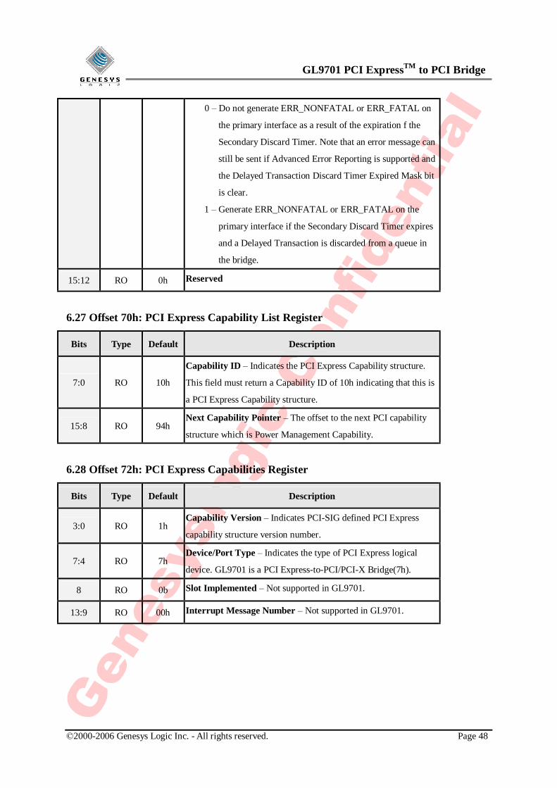
0 – Do not generate ERR_NONFATAL or ERR_FATAL on
the primary interface as a result of the expiration f the
Secondary Discard Timer. Note that an error message can
still be sent if Advanced Error Reporting is supported and
the Delayed Transaction Discard Timer Expired Mask bit
is clear.
1 – Generate ERR_NONFATAL or ERR_FATAL on the
primary interface if the Secondary Discard Timer expires
and a Delayed Transaction is discarded from a queue in
the bridge.
15:12 RO 0h Reserved
6.27 Offset 70h: PCI Express Capability List Register
Bits Type Default Description
7:0 RO 10h
Capability ID – Indicates the PCI Express Capability structure.
This field must return a Capability ID of 10h indicating that this is
a PCI Express Capability structure.
15:8 RO 94h Next Capability Pointer – The offset to the next PCI capability
structure which is Power Management Capability.
6.28 Offset 72h: PCI Express Capabilities Register
Bits Type Default Description
3:0 RO 1h Capability Version – Indicates PCI-SIG defined PCI Express
capability structure version number.
7:4 RO 7h Device/Port Type – Indicates the type of PCI Express logical
device. GL9701 is a PCI Express-to-PCI/PCI-X Bridge(7h).
8 RO 0b Slot Implemented – Not supported in GL9701.
13:9 RO 00h Interrupt Message Number – Not supported in GL9701.

GL9701 PCI ExpressTM to PCI Bridge
©2000-2006 Genesys Logic Inc. - All rights reserved. Page 49
6.29 Offset 74h: PCI Express Device Capabilities Register
Bits Type Default Description
2:0 RO 010b Max_Payload_Size Supported –512 bytes max payload size is
supported.
4:3 RO 00b
Phantom Functions Supported –No function number bits used
for Phantom Functions; device may implement all function
numbers.
5 RO 0b Extended Tag Field Supported –5-bit Tag field supported
8:6 RO 111b
Endpoint L0s Acceptable Latency –The acceptable total latency
that an Endpoint can withstand due to the transition from L0s state
to the L0 state is more than 4 µs.
11:9 RO 111b
Endpoint L1 Acceptable Latency –The acceptable latency that an
Endpoint can withstand due to the transition from L1 state to the
L0 state is more than 64 µs.
12 RO 0b Attention Button Present – Not supported.
13 RO 0b Attention Indicator Present – Not supported.
14 RO 0b Power Indicator Present – Not supported.
17:15 RsvdP 000b RsvdP
25:18 RO 00h
Captured Slot Power Limit Value – In combination with the Slot
Power Limit Scale value, specifies the upper limit on power
supplied by slot. This value is set by the Set_Slot_Power_Limit
Message
27:26 RO 00b
Captured Slot Power Limit Scale – Specifies the scale used for
the Slot Power Limit Value. This value is set by the
Set_Slot_Power_Limit Message.
6.30 Offset 78h: PCI Express Device Control Register
Bits Type Default Description
0 RW 0b Correctable Error Reporting Enable – This bit controls
reporting of correctable errors.

GL9701 PCI ExpressTM to PCI Bridge
©2000-2006 Genesys Logic Inc. - All rights reserved. Page 50
1 RW 0b Non-Fatal Error Reporting Enable – This bit controls reporting
of Non-fatal errors.
2 RW 0b Fatal Error Reporting Enable – This bit controls reporting of
Fatal errors.
3 RW 0b Unsupported Request Reporting Enable – This bit enables
reporting of Unsupported Requests when set.
4 RW 0b
Enable Relaxed Ordering – If this bit is set, the device is
permitted to set the Relaxed Ordering bit in the Attributes field of
transactions it initiates that do not require strong write ordering.
7:5 RW 000b
Max_Payload_Size – This field sets maximum TLP payload
size for the device. Permissible values that can be programmed are
indicated by the Max_Payload_Size
Supported in the Device Capabilities register.
8 RO 0b Extended Tag Field Enable – Not supported.
9 RO 0b Phantom Functions Enable – Not supported.
10 RO 0b Auxiliary (AUX) Power PM Enable – Not su[pported.
11 RO 0b Enable No Snoop – GL9701 never sets the No Snoop attribute in
transactions it initiates.
14:12 RW 010b
Max_Read_Request_Size – This field sets the maximum Read
Request size for the Device as a Requester. The Device must not
generate read requests with size exceeding the set value.
15 RsvdP 0b RsvdP
6.31 Offset 7ah: PCI Express Device Status Register
Bits Type Default Description
0 RW1C 0b
Correctable Error Detected – This bit indicates status of
correctable errors detected. Errors are logged in this register
regardless of whether error reporting is enabled or not in the
Device Control register.
1 RW1C 0b
Non-Fatal Error Detected – This bit indicates status of Nonfatal
errors detected. Errors are logged in this register
regardless of whether error reporting is enabled or not in the

GL9701 PCI ExpressTM to PCI Bridge
©2000-2006 Genesys Logic Inc. - All rights reserved. Page 51
Device Control register.
2 RW1C 0b
Fatal Error Detected – This bit indicates status of Fatal errors
detected. Errors are logged in this register regardless of whether
error reporting is enabled or not in the Device Control register.
3 RW1C 0b
Unsupported Request Detected – This bit indicates that the
device received an Unsupported Request. Errors are logged in this
register regardless of whether error reporting is enabled or not in
the Device Control register.
4 RO 0b AUX Power Detected – Devices that require AUX power report
this bit as set if AUX power is detected by the device.
5 RO 0b
Transactions Pending – This bit when set indicates that the
device has issued Non-Posted Requests which have not been
completed. A device reports this bit cleared only when all
outstanding Non-Posted Requests have completed or have been
terminated by the Completion Timeout mechanism.
15:6 RsvdZ 000h RsvdZ
6.32 Offset 7ch: PCI Express Link Capabilities Register
Bits Type Default Description
3:0 RO 0001b
Maximum Link Speed – This field indicates the maximum Link
speed of the given PCI Express Link. Defined encodings are:
0001b 2.5 Gb/s Link
9:4 RO 00001b Maximum Link Width – This field indicates the maximum width
of the given PCI Express Link.
11:10 RO 00b Active State Power Management (ASPM) Support –
Not supported
14:12 RO 111b L0s Exit Latency – This field indicates the L0s exit latency for the
given PCI Express Link.
17:15 RO 111b L1 Exit Latency – This field indicates the L1 exit latency for the
given PCI Express Link.
23:18 RsvdP 00h RsvdP
31:24 RO 01h Port Number – This field indicates the PCI Express Port

GL9701 PCI ExpressTM to PCI Bridge
©2000-2006 Genesys Logic Inc. - All rights reserved. Page 52
number for the given PCI Express Link.
6.33 Offset 80h: PCI Express Link Control Register
Bits Type Default Description
1:0 RO 00b Active State Power Management (ASPM) Control –
GL9701 does not support ASPM.
2 RsvdP 0b RsvdP
3 RO 0b
Read Completion Boundary (RCB) – Indicates the RCB value
for the Root Port. Defined encodings are:
0b : 64 byte
1b : 128 byte
4 RW 0b Link Disable – This bit disables the Link when set to 1b.
5 RW 0b Retrain Link – A write of 1b to this bit initiates Link retraining by
directing the Physical Layer LTSSM to the Recovery state.
6 RW 0b
Common Clock Configuration – This bit when set indicates
that this component and the component at the opposite end of
this Link are operating with a distributed common reference clock.
A value of 0b indicates that this component and the component at
the opposite end of this Link are operating with asynchronous
reference clock.
7 RW 0b
Extended Synch – This bit when set forces the transmission of
4096 FTS ordered sets in the L0s state followed by a single SKP
ordered set prior to entering the L0 state, and the transmission of
1024 TS1 ordered sets in the L1 state prior to entering the
Recovery state.
15:8 RsvdP 00h RsvdP
6.34 Offset 82h: PCI Express Link Status Register
Bits Type Default Description
3:0 RO 0h Link Speed – This field indicates the negotiated Link speed of the
given PCI Express Link.Defined encodings are:

GL9701 PCI ExpressTM to PCI Bridge
©2000-2006 Genesys Logic Inc. - All rights reserved. Page 53
0001b 2.5 Gb/s PCI Express Link
9:4 RO 000001b Negotiated Link Width – This field indicates the negotiated
width of the given PCI Express Link.
10 RO 0b Training Error – This read-only bit indicates that a Link training
error occurred.
11 RO 0b
Link Training – This read-only bit indicates that Link training is
in progress (Physical Layer LTSSM in Configuration or
Recovery state) or that 1b was written to the Retrain Link bit but
Link training has not yet begun. Hardware clears this bit once Link
training is complete.
12 RO 1b
Slot Clock Configuration – This bit indicates that the
component uses the same physical reference clock that the
platform provides on the connector.
15:13 RsvdZ 000b RsvdZ
6.35 Offset 94h: PM Capability ID Register
Bits Type Default Description
7:0 RO 01h ID – This field, when “01h” identifies the linked list item as being
the PCI Power Management registers.
6.36 Offset 95h: PM Next Pointer Register
Bits Type Default Description
7:0 RO a0h Next Item Pointer – Next capability is Slot Numbering capability.
6.37 Offset 96h: Power Management Capabilities Register
Bits Type Default Description
2:0 RO 010b
Version – A value of 010b indicates that this function complies
with Revision 1.1 of the PCI Power Management Interface
Specification.
3 RO 0b PME Clock – Indicates that no PCI clock is required for the
GL9701 PCI ExpressTM to PCI Bridge
©2000-2006 Genesys Logic Inc. - All rights reserved. Page 54
function to generate PME#.
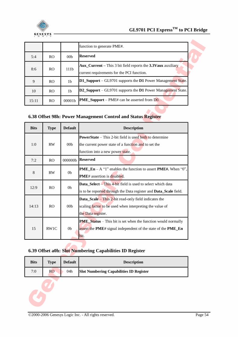
5:4 RO 00b Reserved
8:6 RO 111b Aux_Current – This 3 bit field reports the 3.3Vaux auxiliary
current requirements for the PCI function.
9 RO 1b D1_Support – GL9701 supports the D1 Power Management State.
10 RO 1b D2_Support – GL9701 supports the D1 Power Management State.
15:11 RO 00001b PME_Support – PME# can be asserted from D0.
6.38 Offset 98h: Power Management Control and Status Register
Bits Type Default Description
1:0 RW 00b
PowerState – This 2-bit field is used both to determine
the current power state of a function and to set the
function into a new power state.
7:2 RO 000000b Reserved
8 RW 0b PME_En – A “1” enables the function to assert PME#. When “0”,
PME# assertion is disabled.
12:9 RO 0h Data_Select – This 4-bit field is used to select which data
is to be reported through the Data register and Data_Scale field.
14:13 RO 00b
Data_Scale – This 2-bit read-only field indicates the
scaling factor to be used when interpreting the value of
the Data register.
15 RW1C 0b
PME_Status – This bit is set when the function would normally
assert the PME# signal independent of the state of the PME_En
bit.
6.39 Offset a0h: Slot Numbering Capabilities ID Register
Bits Type Default Description
7:0 RO 04h Slot Numbering Capabilities ID Register

GL9701 PCI ExpressTM to PCI Bridge
©2000-2006 Genesys Logic Inc. - All rights reserved. Page 55
6.40 Offset a1h: Slot Numbering Pointer to Next ID Register
Bits Type Default Description
7:0 RO 00h Pointer to Next Capabilities
6.41 Offset a2h: Slot Numbering Expansion Slot Register
Bits Type Default Description
4:0 RO 3h
Expansion Slots Provided – Contains the binary value of the
number of PCI expansion slots located directly on the secondary
interface of this bridge.
5 RO 1b
First in Chassis – If this bit is set, it indicates that this bridge is
the first in an expansion chassis. A bridge with this bit set
indicates the existence of an expansion chassis that requires a
unique chassis number.
0 – This is not a parent bridge.
1 – This is a parent bridge.
7:6 RO 00b Reserved
6.42 Offset a3h: Slot Numbering Chassis Number Register
Bits Type Default Description
7:0 RW 00h Chassis Number: Contains the physical chassis number for the
slots on the bridge’s secondary interface.
6.43 Offset 100h: Advanced Error Reporting Enhanced Capability Header Register
Bits Type Default Description
15:0 RO 0001h PCI Express Extended Capability ID
19:16 RO 1h Capability Version
31:20 RO 150h Next Capability Offset – Next capability is Device Serial Number
Capability.

GL9701 PCI ExpressTM to PCI Bridge
©2000-2006 Genesys Logic Inc. - All rights reserved. Page 56
6.44 Offset 104h: Uncorrectable Error Status Register
Bits Type Default Description
0 RW1C 0 Training Error Status
4 RW1C 0 Data Link Protocol Error Status
12 RW1C 0 Poisoned TLP Status
13 RW1C 0 Flow Control Protocol Error Status
14 RW1C 0 Completion Timeout Status
15 RW1C 0 Completer Abort Status
16 RW1C 0 Unexpected Completion Status
17 RW1C 0 Receiver Overflow Status
18 RW1C 0 Malformed TLP Status
19 RW1C 0 ECRC Error Status
20 RW1C 0 Unsupported Request Error Status
6.45 Offset 108h: Uncorrectable Error Mask Register
Bits Type Default Description
0 RWS 0 Training Error Mask
4 RWS 0 Data Link Protocol Error Mask
12 RWS 0 Poisoned TLP Mask
13 RWS 0 Flow Control Protocol Error Mask
14 RWS 0 Completion Timeout Mask
15 RWS 0 Completer Abort Mask
16 RWS 0 Unexpected Completion Mask
17 RWS 0 Receiver Overflow Mask
18 RWS 0 Malformed TLP Mask
19 RWS 0 ECRC Error Mask

GL9701 PCI ExpressTM to PCI Bridge
©2000-2006 Genesys Logic Inc. - All rights reserved. Page 57
20 RWS 0 Unsupported Request Error Mask
6.46 Offset 10ch: Uncorrectable Error Severity Register
Bits Type Default Description
0 RWS 1 Training Error Severity
4 RWS 1 Data Link Protocol Error Severity
12 RWS 0 Poisoned TLP Severity
13 RWS 1 Flow Control Protocol Error Severity
14 RWS 0 Completion Timeout Error Severity
15 RWS 0 Completer Abort Error Severity
16 RWS 0 Unexpected Completion Error Severity
17 RWS 1 Receiver Overflow Error Severity
18 RWS 1 Malformed TLP Severity
19 RWS 0 ECRC Error Severity
20 RWS 0 Unsupported Request Error Severity
6.47 Offset 110h: Correctable Error Status Register
Bits Type Default Description
0 RW1CS 0 Receiver Error Status
6 RW1CS 0 Bad TLP Status
7 RW1CS 0 Bad DLLP Status
8 RW1CS 0 REPLAY_NUM Rollover Status
12 RW1CS 0 Replay Timer Timeout Status
6.48 Offset 114h: Correctable Error Mask Register
Bits Type Default Description

GL9701 PCI ExpressTM to PCI Bridge
©2000-2006 Genesys Logic Inc. - All rights reserved. Page 58
0 RWS 0 Receiver Error Mask
6 RWS 0 Bad TLP Mask
7 RWS 0 Bad DLLP Mask
8 RWS 0 REPLAY_NUM Rollover Mask
12 RWS 0 Replay Timer Timeout Mask
6.49 Offset 118h: Advanced Error Capabilities and Control Register
Bits Type Default Description
4:0 ROS 00h First Error Pointer – Identifies the bit position of the first error
reported in the Uncorrectable Error Status register.
5 RO 1b ECRC Generation Capable – This bit indicates that
the device is capable of generating ECRC.
6 RWS 0b ECRC Generation Enable – This bit when set
enables ECRC generation.
7 RO 1b ECRC Check Capable – This bit indicates that the
device is capable of checking ECRC.
8 RWS 0b ECRC Check Enable – This bit when set enables
ECRC checking.
6.50 Offset 11ch: Header Log Register
Bits Type Default Description
127:0 ROS 0h Header Log – Header of TLP associated with error
6.51 Offset 12ch: Secondary Uncorrectable Error Status Register
Bits Type Default Description
0 RW1CS 0 Target-Abort on Split Completion Status
1 RW1CS 0 Master-Abort on Split Completion Status
2 RW1CS 0 Received Target-Abort Status

GL9701 PCI ExpressTM to PCI Bridge
©2000-2006 Genesys Logic Inc. - All rights reserved. Page 59
3 RW1CS 0 Received Master-Abort Status
4 RsvdZ 0 Reserved
5 RW1CS 0 Unexpected Split Completion Error Status
6 RW1CS 0 Uncorrectable Split Completion Message Data
Error Status
7 RW1CS 0 Uncorrectable Data Error Status
8 RW1CS 0 Uncorrectable Attribute Error Status
9 RW1CS 0 Uncorrectable Address Error Status
10 RW1CS 0 Delayed Transaction Discard Timer Expired
Status
11 RW1CS 0 PERR# Assertion Detected
12 RW1CS 0 SERR# Assertion Detected (No Header Log)
13 RW1CS 0 Internal Bridge Error Status
6.52 Offset 130h: Secondary Uncorrectable Error Mask Register
Bits Type Default Description
0 RWS 0 Target-Abort on Split Completion Mask
1 RWS 0 Master-Abort on Split Completion Mask
2 RWS 0 Received Target-Abort Mask
3 RWS 1 Received Master-Abort Mask
4 RsvdP 0 Reserved
5 RWS 1 Unexpected Split Completion Error Mask
6 RWS 0 Uncorrectable Split Completion Message Data
Error Mask
7 RWS 1 Uncorrectable Data Error Mask
8 RWS 1 Uncorrectable Attribute Error Mask
9 RWS 1 Uncorrectable Address Error Mask

GL9701 PCI ExpressTM to PCI Bridge
©2000-2006 Genesys Logic Inc. - All rights reserved. Page 60
10 RWS 1 Delayed Transaction Discard Timer Expired
Mask
11 RWS 0 PERR# Assertion Detected Mask
12 RWS 1 SERR# Assertion Detected Mask
13 RWS 0 Internal Bridge Error Mask
6.53 Offset 134h: Secondary Uncorrectable Error Severity Register
Bits Type Default Description
0 RWS 0 Target-Abort on Split Completion Severity
1 RWS 0 Master-Abort on Split Completion Severity
2 RWS 0 Received Target-Abort Severity
3 RWS 0 Received Master-Abort Severity
4 RsvdP 0 Reserved
5 RWS 0 Unexpected Split Completion Error Severity
6 RWS 1 Uncorrectable Split Completion Message Data
Error Severity
7 RWS 0 Uncorrectable Data Error Severity
8 RWS 1 Uncorrectable Attribute Error Severity
9 RWS 1 Uncorrectable Address Error Severity
10 RWS 0 Delayed Transaction Discard Timer Expired
Severity
11 RWS 0 PERR# Assertion Detected Severity
12 RWS 1 SERR# Assertion Detected Severity
13 RWS 0 Internal Bridge Error Severity
6.54 Offset 138h: Secondary Error Capabilities and Control Register
Bits Type Default Description
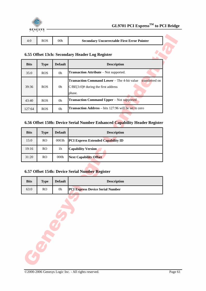
GL9701 PCI ExpressTM to PCI Bridge
©2000-2006 Genesys Logic Inc. - All rights reserved. Page 61
4:0 ROS 00h Secondary Uncorrectable First Error Pointer
6.55 Offset 13ch: Secondary Header Log Register
Bits Type Default Description
35:0 ROS 0h Transaction Attribute – Not supported.
39:36 ROS 0h
Transaction Command Lower – The 4-bit value transferred on
C/BE[3:0]# during the first address
phase.
43:40 ROS 0h Transaction Command Upper – Not supported
127:64 ROS 0h Transaction Address – bits 127:96 will be set to zero
6.56 Offset 150h: Device Serial Number Enhanced Capability Header Register
Bits Type Default Description
15:0 RO 0003h PCI Express Extended Capability ID
19:16 RO 1h Capability Version
31:20 RO 000h Next Capability Offset
6.57 Offset 154h: Device Serial Number Register
Bits Type Default Description
63:0 RO 0h PCI Express Device Serial Number

GL9701 PCI ExpressTM to PCI Bridge
©2000-2006 Genesys Logic Inc. - All rights reserved. Page 62
CHAPTER 7 Electrical Characteristics
7.1 Operation Conditions
Symbol Parameter Min. Typ. Max. Unit
VDD Non-AUX GL9701 Bridge Core Power 1.62 1.8 1.98 Volt
VDD33 Non-AUX PCI Pad Power 2.97 3.3 3.63 Volt
VDD18_AUX AUX GL9701 Bridge Core Power 1.62 1.8 1.98 Volt
VDD33_AUX AUX PCI Pad Power 2.97 3.3 3.63 Volt
AVDDPCI Analog Power for PCI PLL 1.62 1.8 1.98 Volt
VDDPLL Analog power for PLL 1.62 1.8 1.98 Volt
VDDRX Analog Power for RX 1.62 1.8 1.98 Volt
VDDTX Analog Power for TX 1.62 1.8 1.98 Volt
7.2 Differential Transmitter (TX) Output Specification The following table defines the specification of parameters for the differential output at all
Transmitters (TXs). The parameters are specified at the component pins.
Symbol Parameter Min Typ Max Units Comments
UI Unit Interval
399.88
400
400.12 ps Each UI is 400 ps
+/-300 ppm. UI does
not account for SSC
dictated variations.
See Note 1.
VTX-DIFFp-p
Differential
Peak
to Peak Output
Voltage
0.800 1.2 V VTX-DIFFp-p =
2*|VTX-D+ - VTX-D-|
See Note 2.
VTX-DE-RATIO
De-Emphasized
Differential
Output Voltage
(Ratio)
-3.0 -3.5 -4.0 dB This is the ratio of the
VTX-DIFFp-p of the
second and following
bits after a transition
divided by the
VTX-DIFFp-p of the
first bit after a
transition.

GL9701 PCI ExpressTM to PCI Bridge
©2000-2006 Genesys Logic Inc. - All rights reserved. Page 63
See Note 2.
TTX-EYE
Minimum TX
Eye Width
0.75 UI The maximum
Transmitter
jitter can be derived as
TTX-MAX-JITTER =
1 - TTX-EYE = 0.25
UI. This parameter is
measured with the
equivalent of a zero
jitter reference clock.
See Notes 2 and 3.
TTX-EYEMEDIAN-
to-MAXJITTER
Maximum time
between the
jitter median and
maximum
deviation from
the median.
0.125 UI Jitter is defined as the
measurement variation
of the crossing points
(VTX-DIFF = 0 V)
in relation to recovered
TX UI. To be
measured after the
clock recovery
function.
See Notes 2 and 3.
TTX-RISE,
TTX-FALL
D+/D- TX
Output
Rise/Fall Time
0.125 UI See Notes 2 and 5.
VTX-CM-ACp
RMS AC Peak
Common Mode
Output Voltage
20 mV VTX-CM-ACp =
RMS(|VTX-D+ +
VTX-D-|/2 –
VTX-CM-DC)
VTX-CM-DC =
DC(avg) of |VTX-D+
+VTX-D-|/2
See Note 2.
VTX-CM-DCACTIVE-
IDLEDELTA
Absolute Delta
of DC Common
0 100 mV |VTX-CM-DC [during
L0] – VTX-CM-Idle-
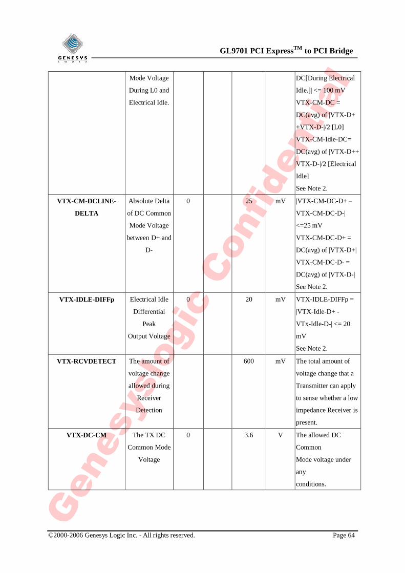
GL9701 PCI ExpressTM to PCI Bridge
©2000-2006 Genesys Logic Inc. - All rights reserved. Page 64
Mode Voltage
During L0 and
Electrical Idle.
DC[During Electrical
Idle.]| <= 100 mV
VTX-CM-DC =
DC(avg) of |VTX-D+
+VTX-D-|/2 [L0]
VTX-CM-Idle-DC=
DC(avg) of |VTX-D++
VTX-D-|/2 [Electrical
Idle]
See Note 2.
VTX-CM-DCLINE-
DELTA
Absolute Delta
of DC Common
Mode Voltage
between D+ and
D-
0 25 mV |VTX-CM-DC-D+ –
VTX-CM-DC-D-|
<=25 mV
VTX-CM-DC-D+ =
DC(avg) of |VTX-D+|
VTX-CM-DC-D- =
DC(avg) of |VTX-D-|
See Note 2.
VTX-IDLE-DIFFp
Electrical Idle
Differential
Peak
Output Voltage
0 20 mV VTX-IDLE-DIFFp =
|VTX-Idle-D+ -
VTx-Idle-D-| <= 20
mV
See Note 2.
VTX-RCVDETECT
The amount of
voltage change
allowed during
Receiver
Detection
600 mV The total amount of
voltage change that a
Transmitter can apply
to sense whether a low
impedance Receiver is
present.
VTX-DC-CM
The TX DC
Common Mode
Voltage
0 3.6 V The allowed DC
Common
Mode voltage under
any
conditions.

GL9701 PCI ExpressTM to PCI Bridge
©2000-2006 Genesys Logic Inc. - All rights reserved. Page 65
ITX-SHORT
TX Short Circuit
Current Limit
90 mA The total current the
Transmitter can
provide when shorted
to its ground.
TTX-IDLE-MIN
Minimum time
spent in
Electrical Idle
50 UI Minimum time a
Transmitter must be in
Electrical Idle Utilized
by the Receiver to start
looking for an
Electrical
Idle Exit after
successfully
receiving an Electrical
Idle
ordered set.
TTX-IDLE-SETTO-
IDLE
Maximum time
to transition to a
valid Electrical
Idle after
sending an
Electrical Idle
ordered set
20 UI After sending an
Electrical
Idle ordered set, the
Transmitter must meet
all
Electrical Idle
specifications
within this time. This
is
considered a debounce
time for the
Transmitter to meet
Electrical Idle after
transitioning from L0.
TTX-IDLE-TODIFF-
DATA
Maximum time
to transition to
valid TX
specifications
after leaving an
20 UI Maximum time to
meet all TX
specifications when
transitioning from
Electrical Idle to
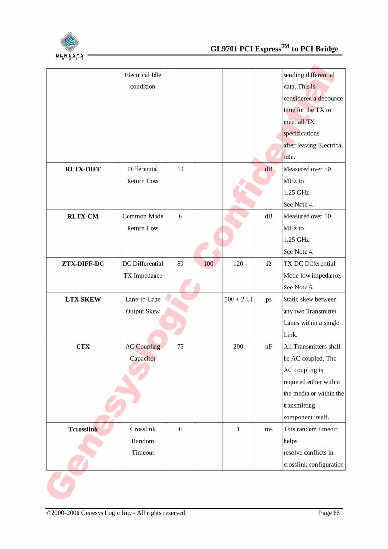
GL9701 PCI ExpressTM to PCI Bridge
©2000-2006 Genesys Logic Inc. - All rights reserved. Page 66
Electrical Idle
condition
sending differential
data. This is
considered a debounce
time for the TX to
meet all TX
specifications
after leaving Electrical
Idle.
RLTX-DIFF
Differential
Return Loss
10 dB Measured over 50
MHz to
1.25 GHz.
See Note 4.
RLTX-CM
Common Mode
Return Loss
6 dB Measured over 50
MHz to
1.25 GHz.
See Note 4.
ZTX-DIFF-DC
DC Differential
TX Impedance
80 100 120 Ω
TX DC Differential
Mode low impedance.
See Note 6.
LTX-SKEW
Lane-to-Lane
Output Skew
500 + 2 UI
ps Static skew between
any two Transmitter
Lanes within a single
Link.
CTX
AC Coupling
Capacitor
75 200 nF All Transmitters shall
be AC coupled. The
AC coupling is
required either within
the media or within the
transmitting
component itself.
Tcrosslink
Crosslink
Random
Timeout
0 1 ms This random timeout
helps
resolve conflicts in
crosslink configuration

GL9701 PCI ExpressTM to PCI Bridge
©2000-2006 Genesys Logic Inc. - All rights reserved. Page 67
by eventually resulting
in only one
Downstream and one
Upstream Port.
Notes:
1. No test load is necessarily associated with this value.
2. Specified at the measurement point into a timing and voltage compliance test load and measured using the
clock recovery function.
3. A TTX-EYE = 0.75 UI provides for a total sum of deterministic and random jitter budget of
TTX-JITTER-MAX = 0.25 UI for the Transmitter using the clock recovery function. The
TTX-EYE-MEDIAN-to-MAX-JITTER specification ensures a jitter distribution in which the median and the
maximum deviation from the median is less than half of the total TX jitter budget using the clock recovery
function. It should be noted that the median is not the same as the mean. The jitter median describes the point
in time where the number of jitter points on either side is approximately equal as opposed to the averaged time
value. This parameter is measured with the equivalent of a zero jitter reference clock. The TTX-EYE
measurement is to be met at the target bit error rate. The TTX-EYE-MEDIAN-to-MAX-JITTER is to be met
using the compliance pattern at a sample size of 1,000,000 UI.
4. The Transmitter input impedance shall result in a differential return loss greater than or equal to 10 dB with a
differential test input signal no less than 200 mV (peak value, 400 mV differential peak to peak) swing around
ground applied to D+ and D- lines and a common mode
return loss greater than or equal to 6 dB over a frequency range of 50 MHz to 1.25 GHz. This input impedance
requirement applies to all valid input levels. The reference impedance for return loss measurements is 50 Ω to
ground for both the D+ and D- line. Note that the series capacitors CTX is optional for the return loss
measurement.
5. Measured between 20-80% at Transmitter package pins into a test load for both VTX-D+ and VTX-D-.
6. ZTX-DIFF-DC is the small signal resistance of the transmitter measured at a DC operating point that is
equivalent to that established by connecting a 100 Ω resistor from D+ and D- while the TX is driving a static
logic one or logic zero. Equivalently, this parameter can be derived by measuring the RMS voltage of the TX
while transmitting a test pattern into two different differential terminations that are
near 100 Ω. Small signal resistance is measured by forcing a small change in differential voltage and dividing
this by the corresponding change in current.

GL9701 PCI ExpressTM to PCI Bridge
©2000-2006 Genesys Logic Inc. - All rights reserved. Page 68
7.3 Differential Receiver (RX) Input Specification
The following table defines the specification of parameters for all differential Receivers (RXs). The
parameters are specified at the component pins.
Symbol Parameter Min Typ Max Units Comments
Unit Interval
399.88 400 400.12 ps The UI is 400 ps +/- 300 ppm. UI
does not account for SSC dictated
variations.
See Note 7.
VRX-DIFFp-p
Differential
Input Peak to
Peak Voltage
0.175 1.2 V VRX-DIFFp-p =
2*|VRX-D+ -VRX-D-|
See Note 8.
TRX-EYE
Minimum
Receiver Eye
Width
0.4 UI The maximum interconnect
media and Transmitter jitter that can
be tolerated by the Receiver can be
derived as TRX-MAX-JITTER =
1 - TRX-EYE = 0.6 UI.
See Notes 8, 9, and 10.
TRX-EYE-MEDI
AN-to-
MAX-JITTER
Maximum time
between the
jitter median
and maximum
deviation from
the median.
0.3 UI Jitter is defined as the measurement
variation of the crossing points
(VRX-DIFFp-p = 0 V) in relation
to a recovered TX UI. To be
measured after the clock recovery
function.
See Notes 8 and 9.
VRX-CM-ACp
AC Peak
Common Mode
Input Voltage
150 mV VRX-CM-AC =
|VRX-D+ + VRX-D-|/2 –
VRX-CM-DC
VRX-CM-DC = DC(avg) of
|VRX-D++ VRX-D-|/2
See Note 8.
RLRX-DIFF
Differential
Return Loss
10 dB Measured over 50 MHz to
1.25 GHz.
See Note 11.
RLRX-CM Common Mode 6 dB Measured over 50 MHz to
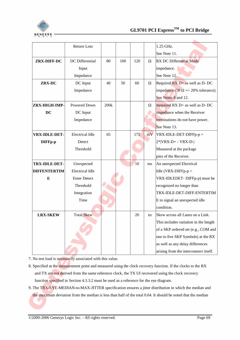
GL9701 PCI ExpressTM to PCI Bridge
©2000-2006 Genesys Logic Inc. - All rights reserved. Page 69
Return Loss
1.25 GHz.
See Note 11.
ZRX-DIFF-DC
DC Differential
Input
Impedance
80 100 120 Ω
RX DC Differential Mode
impedance.
See Note 12.
ZRX-DC
DC Input
Impedance
40 50 60 Ω
Required RX D+ as well as D- DC
impedance (50 Ω +/- 20% tolerance).
See Notes 8 and 12.
ZRX-HIGH-IMP-
DC
Powered Down
DC Input
Impedance
200k Ω
Required RX D+ as well as D- DC
impedance when the Receiver
terminations do not have power.
See Note 13.
VRX-IDLE-DET-
DIFFp-p
Electrical Idle
Detect
Threshold
65 175 mV VRX-IDLE-DET-DIFFp-p =
2*|VRX-D+ - VRX-D-|
Measured at the package
pins of the Receiver.
TRX-IDLE-DET-
DIFFENTERTIM
E
Unexpected
Electrical Idle
Enter Detect
Threshold
Integration
Time
10 ms An unexpected Electrical
Idle (VRX-DIFFp-p <
VRX-IDLEDET- DIFFp-p) must be
recognized no longer than
TRX-IDLE-DET-DIFF-ENTERTIM
E to signal an unexpected idle
condition.
LRX-SKEW
Total Skew
20 ns Skew across all Lanes on a Link.
This includes variation in the length
of a SKP ordered set (e.g., COM and
one to five SKP Symbols) at the RX
as well as any delay differences
arising from the interconnect itself.
7. No test load is necessarily associated with this value.
8. Specified at the measurement point and measured using the clock recovery function. If the clocks to the RX
and TX are not derived from the same reference clock, the TX UI recovered using the clock recovery
function specified in Section 4.3.3.2 must be used as a reference for the eye diagram.
9. The TRX-EYE-MEDIAN-to-MAX-JITTER specification ensures a jitter distribution in which the median and
the maximum deviation from the median is less than half of the total 0.64. It should be noted that the median

GL9701 PCI ExpressTM to PCI Bridge
©2000-2006 Genesys Logic Inc. - All rights reserved. Page 70
is not the same as the mean. The jitter median describes the point in time where the number of jitter points on
either side is approximately equal as opposed to the averaged time value.
The RX UI recovered using the clock recovery function must be used as the reference for the eye diagram.
This parameter is measured with the equivalent of a zero jitter reference clock. The TRX-EYE measurement is
to be met at the target bit error rate. The TRX-EYE-MEDIAN-to-MAX-JITTER specification is to be met
using the compliance pattern at a sample size of 1,000,000 UI.
10. See the PCI Express Jitter and BER white paper for more details on the Rx-Eye measurement.
11. The Receiver input impedance shall result in a differential return loss greater than or equal to 10 dB with a
differential test input signal of no less than 200 mV (peak value, 400 mV differential peak to peak) swing
around ground applied to D+ and D- lines and a common mode return loss greater than or equal to 6 dB (no
bias required) over a frequency range of 50 MHz to 1.25 GHz. This input impedance requirement applies to
all valid input levels. The reference impedance for return loss measurements for is 50 Ω to ground for both
the D+ and D- line. Note that the series capacitors CTX is optional for the return loss measurement.
12. Impedance during all LTSSM states. When transitioning from a Fundamental Reset to Detect (the initial state
of the LTSSM) there is a 5 ms transition time before Receiver termination values must be met on all
un-configured Lanes of a Port.
13. The RX DC Common Mode Impedance that exists when no power is present or Fundamental Reset is
asserted. This helps ensure that the Receiver Detect circuit will not falsely assume a Receiver is powered on
when it is not. This term must be measured at 200 mV above the RX ground.
7.4 PCI Interface DC Specifications
Symbol Parameter Condition Min. Max Units Notes
Vcc Supply Voltage 3.0 3.6 V
Vih Input High Voltage 0.5Vcc Vcc + 0.5 V
Vil Input Low Voltage -0.5 0.3Vcc V
Vipu Input Pull-up
Voltage
0.7Vcc V 1
Iil Input Leakage
Current
0 < Vin < Vcc +10 μA 2
Voh Output High Voltage Iout = -500μA 0.9Vcc V
Vol Output Low Voltage Iout = 1500μA 0.1Vcc V
Cin Input Pin
Capacitance
10 pF 3
Cclk CLK Pin 5 12 pF

GL9701 PCI ExpressTM to PCI Bridge
©2000-2006 Genesys Logic Inc. - All rights reserved. Page 71
Capacitance
CIDSEL IDSEL Pin
Capacitance
8 pF 4
Lpin Pin Inductance 20 nH 5
IOff PME# input leakage
Vo 3.6 V≦
Vcc off or
floating
- 1 μA
6
Notes:
1. This specification should be guaranteed by design. It is the minimum voltage to which pull-up resistors are
calculated to pull a floated network. Applications sensitive to static power utilization must assure that the
input buffer is conducting minimum current at this input voltage.
2. Input leakage currents include hi-Z output leakage for all bi-directional buffers with tri-state outputs.
3. Absolute maximum pin capacitance for a PCI input is 10 pF (except for CLK, SMBDAT, and SMBCLK) with
an exception granted to system board-only devices up to 16 pF in order to accommodate PGA packaging. This
would mean, in general, that components for add-in cards need to use alternatives to ceramic PGA packaging;
i.e., PQFP, SGA, etc. Pin capacitance for SMBCLK and SMBDAT is not specified; however, the maximum
capacitive load is specified for the add-in card in Section 8.2.5.
4. Lower capacitance on this input-only pin allows for non-resistive coupling to AD[xx].
5. This is a recommendation, not an absolute requirement. The actual value should be provided with the
component data sheet.
6. This input leakage is the maximum allowable leakage into the PME# open drain driver when power is
removed from Vcc of the component. This assumes that no event has occurred to cause the device to attempt
to assert PME#.
7.5 PCI Interface AC Specifications
Symbol Parameter Condition Min. Max Units Notes
0 < Vout 0.3Vcc≦ -12Vcc mA 1
0.3Vcc<Vout<0.9Vcc -17.1(Vcc-Vout) mA 1
Ioh(AC)
Switching
Current High
0.7Vcc < Vout < Vcc Eqt'n C 1, 2
Vcc >Vout 0.6Vcc≧ 16Vcc mA 1
0.6Vcc>Vout>0.1Vcc 26.7Vout mA 1
Iol(AC)
Switching
Current Low
0.18Vcc>Vout>0 Eqt'n D 1, 2

GL9701 PCI ExpressTM to PCI Bridge
©2000-2006 Genesys Logic Inc. - All rights reserved. Page 72
Icl
Low Clamp
Current
-3 < Vin ≤-1
-25+(Vin+1)/0.015
mA
Ich
High Clamp
Current
Vcc+4 > Vin ≥Vcc+1
25+(Vin-Vcc-1)/0.015
mA
slewr
Output Rise
Slew Rate
0.2Vcc - 0.6Vcc load
1 4 V/ns
3
slewf
Output Fall
Slew Rate
0.6Vcc - 0.2Vcc load
1 4 V/ns
3
7.6 Clock and Reset Specifications
Symbol Parameter Min Max Units Notes
Tcyc CLK Cycle Time 30 ∞ ns 1
Thigh CLK High Time 11 ns
Tlow CLK Low Time 11 ns
- CLK Slew Rate 1 4 V/ns 2
- RST#SlewRate 50 - mV/ns 3
Notes:
1. In general, all PCI components must work with any clock frequency between nominal DC and 33 MHz.
Device operational parameters at frequencies under 16 MHz may be guaranteed by design rather than by
testing. The clock frequency may be changed at any time during the operation of the system so long as the
clock edges remain "clean" (monotonic) and the minimum cycle and high and low times are not violated. For
example, the use of spread spectrum techniques to reduce EMI emissions is included in this requirement.
GL9701 PCI ExpressTM to PCI Bridge
©2000-2006 Genesys Logic Inc. - All rights reserved. Page 73
Refer to Section 7.6.4.1 for the spread spectrum requirements for 66 MHz. The clock may only be stopped in a
low state. A variance on this
specification is allowed for components designed for use on the system board only. These components may
operate at any single fixed frequency up to 33 MHz and may enforce a policy of no frequency changes.
2. Rise and fall times are specified in terms of the edge rate measured in V/ns. This slew rate must be met across
the minimum peak-to-peak portion of the clock waveform as shown in Figure 4-7.
3. The minimum RST# slew rate applies only to the rising (deassertion) edge of the reset signal and ensures that
system noise cannot render an otherwise monotonic signal to appear to bounce in the switching range. RST#
waveforms and timing are discussed in Section 4.3.2.

GL9701 PCI ExpressTM to PCI Bridge
©2000-2006 Genesys Logic Inc. - All rights reserved. Page 74
CHAPTER 8 Package Dimension
CONTROL DIMENSIONS ARE IN MILLIMETERS.
SYMBOL MILLIMETER INCHMIN. NOM. MAX. MAX.MIN. NOM.
AA1A2DE
D1E1
R2R1
cLL1Sbe
aaabbbcccddd
D2E2
TOLERANCES OF FORM AND POSITION
16.00 BASIC16.00 BASIC14.00 BASIC14.00 BASIC
0.630 BASIC0.630 BASIC0.551 BASIC0.551 BASIC
0.051.35 1.40
1.600.151.45
001111
3.5
1212
7
1313
0.080.08
0.20 0.0030.003
0.008001111
3.5
1212
7
1313
0.0630.0060.0570.055
0.0020.053
0.200.200.080.07
0.0080.0080.0030.003
0.40 BASIC
12.40 BASIC12.40 BASIC
0.016 BASIC
0.488 BASIC0.488 BASIC
1.00 REF 0.039 REF
0.090.45
0.200.13
0.60
0.16
0.200.75
0.23
0.0040.018
0.0080.005
0.024
0.006
0.0080.030
0.009
0-
02-03-
01-NOTES :
1.
2.
DIMENSIONS D1 AND E1 DO NOT INCLUDEMOLD PROTRUSION. ALLOWABLEPROTRUSION IS 0.25 mm PER SIDE. D1 ANDE1 ARE MAXIMUM PLASTIC BODY SIZEDIMENSIONS INCLUDING MOLD MISMATCH.
DIMENSION b DOES NOT INCLUDE DAMBARPROTRUSION. ALLOWABLE DAMBARPROTRUSION SHALL NOT CAUSE THE LEADWIDTH TO EXCEED THE MAXIMUM bDIMENSION BY MORE THAN 0.08mm.DAMBAR CAN NOT BE LOCATED ON THELOWER RADIUS OR THE FOOT.
SEATINGPLANE
C
Cccc
01-
0-
A
A2 A1
ce
D1
D2
b
D
A B
BA D
DC
H
aaa
bbb
ddd
4X
4X
M C BA s sD
A B
D
1
128
32
33
64
6596
97
GAGE PLANE
R1
R2
0.25mmS L
03-
02-
H
GL9701AAAAAAAGAA
YWWXXXXXXXXDate Code Lot Code
InternalNo.
CodeNo.
GreenPackage
Figure 8.1-GL9701 128 Pin LQFP Package

GL9701 PCI ExpressTM to PCI Bridge
©2000-2006 Genesys Logic Inc. - All rights reserved. Page 75
CHAPTER 9 ORDERING INFORMATION
Table 9.1-Ordering Information
Part Number Package Green Version Status
GL9701-MXG 128-pin LQFP Green Package XX Available