global view of international standards and measurements
TRANSCRIPT

1
30 August 2010
COMS2010 Commercialization of Micro-Nano Systems Conference29 August – 2 September, Albuquerque, NM
Global View of International Standards and Measurements:Challenges and Concerns for Nanotechnologies
Herbert S. BennettNIST Fellow and Executive AdvisorSemiconductor Electronics Division
National Institute of Standards and TechnologyGaithersburg, MD 20899

2
Outline
• Why Standards Are Important• IEC TC 113 Scope, and Working
Groups• ISO TC 229 Scope, and Working
Groups
• Examples of Progress
• Grand Challenges• Invitation to Contribute
3
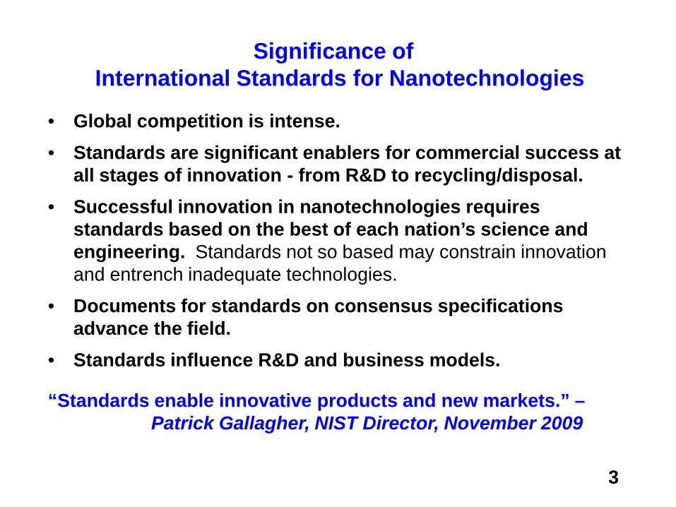
• Global competition is intense. • Standards are significant enablers for commercial success at
all stages of innovation - from R&D to recycling/disposal.• Successful innovation in nanotechnologies requires
standards based on the best of each nation’s science and engineering. Standards not so based may constrain innovation and entrench inadequate technologies.
• Documents for standards on consensus specifications advance the field.
• Standards influence R&D and business models.
“Standards enable innovative products and new markets.” –Patrick Gallagher, NIST Director, November 2009
Significance of International Standards for Nanotechnologies
4
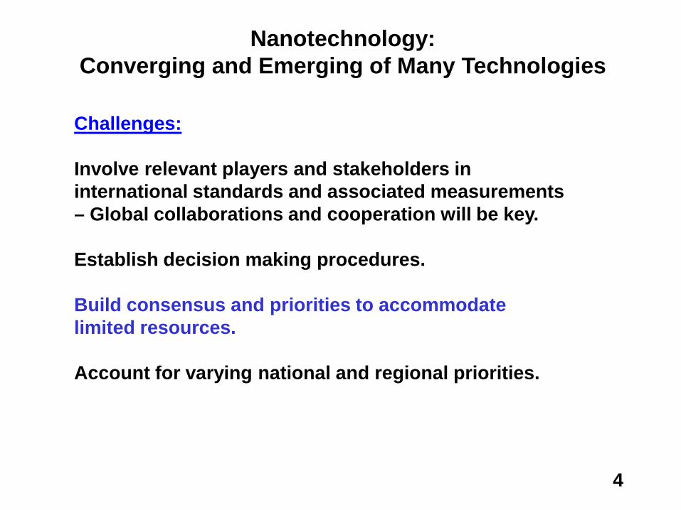
Challenges:
Involve relevant players and stakeholders in international standards and associated measurements – Global collaborations and cooperation will be key.
Establish decision making procedures.
Build consensus and priorities to accommodatelimited resources.
Account for varying national and regional priorities.
Nanotechnology:Converging and Emerging of Many Technologies

5
IEC TC 113 on Nano-electrotechnologies
ScopeEstablished in 2007The scope of TC 113 is “Standardization of the technologies relevant to electrical and electronic products and systems in the field of nanotechnology in close cooperation with other technical committees of IEC and of the International Standards Organization (ISO) TC 229 on nanotechnologies.”Topics include terminology, measurement, characterization, performance, reliability, durability, environment, health, and safety.

6
Scope (continued)
The standard deliverables will focus on components or intermediate assemblies that are created from nano-scaled materials and processes for electrical or electro-optical applications.
Nano-electrotechnologies will be used in a wide variety of applications. Potential applications include: electronics; optics; magnetics; electromagnetics; electroacoustics; multimedia; telecommunications; and energy production (direct conversion into electrical power as in fuel cells, photovoltaic devices and storage of electrical energy).

7
IEC TC 113 Working Groups
• JWG 1: Terminology and NomenclatureScope: Define and develop unambiguous and uniform terminology and nomenclature in the field of nanotechnologies to facilitate communication and to promote common understanding.
• JWG 2: Measurement and CharacterizationScope: The development of standards for measurement, characterization and test methods for nanotechnologies, taking into consideration needs for metrology and reference materials.
JWG 1/JWG 2 are Joint Working Groups with ISO TC 229 on nanotechnologies.

8
IEC TC 113 Working Groups (continued)
• WG 3: Performance Assessment
Scope: To develop standards for the assessment of performance, reliability, and durability related to the nanotechnology-enabled aspects of components and systems in support of continuous improvement at all stages of the value adding chain. WG 3 considers market demand and technology pull with an emphasis on fabrication, processing and process control, disposal, and recycling.
Six stages of the linear economic model – technical research, technology development, initial deployment, commercialization (large-scale, high-volume manufacturing), end of first use, and end-of-life (disposing and recycling)

9
Terms of Reference for IEC TC 113 WG3 on Performance Assessment
KCC = Key Control Characteristics
KCCs
Nano-Subassembly/Component Product/System
Nano-Device/Structure
Figures of Merit Specifications
To develop standards for the assessment of performance, reliability, and durability related to the nanotechnology-enabledfunctionality of components and systems in support of innovativeelectrotechnical products at all stages of the value added chain:
Raw and/or Recycled Material Process Subassembly
System Integration Product End of First Use End-of-Life (Disposing and Recyling)

10
Goal and Objectives: Build an international consensus among members of the nano-electrotechnologies community for developing standards and related measurements to guide IEC TC 113 WG3 program priorities with its limited resources.
Establish procedures for ranking new documents for comment (DCs) and new work item proposals (NWIPs) in priority order.
Respond to new work item proposals from IEC National Committees.
Identify experts for working groups to improve DCs and complete high-priority NWIPs.
An Example:NIST-Energetics-IEC IEC TC 113 Survey
http://www.nist.gov/eeel/semiconductor/upload/NIST_Energetics_Survey.pdf
11
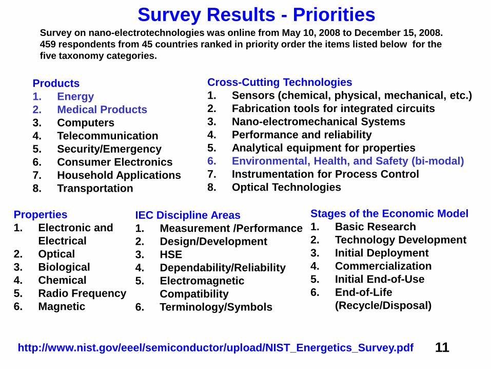
Products1. Energy2. Medical Products 3. Computers4. Telecommunication5. Security/Emergency6. Consumer Electronics7. Household Applications 8. Transportation
http://www.nist.gov/eeel/semiconductor/upload/NIST_Energetics_Survey.pdf
Survey Results - Priorities
Cross-Cutting Technologies1. Sensors (chemical, physical, mechanical, etc.)2. Fabrication tools for integrated circuits 3. Nano-electromechanical Systems 4. Performance and reliability5. Analytical equipment for properties6. Environmental, Health, and Safety (bi-modal)7. Instrumentation for Process Control8. Optical Technologies
Properties1. Electronic and
Electrical 2. Optical 3. Biological4. Chemical5. Radio Frequency 6. Magnetic
Stages of the Economic Model1. Basic Research2. Technology Development 3. Initial Deployment4. Commercialization5. Initial End-of-Use6. End-of-Life
(Recycle/Disposal)
IEC Discipline Areas1. Measurement /Performance2. Design/Development 3. HSE4. Dependability/Reliability5. Electromagnetic
Compatibility6. Terminology/Symbols
Survey on nano-electrotechnologies was online from May 10, 2008 to December 15, 2008.459 respondents from 45 countries ranked in priority order the items listed below for the five taxonomy categories.

12
The 85 respondents who ranked Medical Products the highest also ranked the 8 items for Cross-Cutting Technologies as shown.

13
The 130 respondents who ranked Energy Products the highest also ranked the 8 items for Cross-
Cutting Technologies as shown.

14
The 100 respondents who ranked Sensors the highest also ranked the 8 items for Products as shown.
15
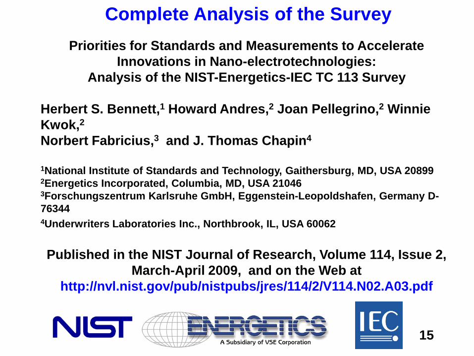
Priorities for Standards and Measurements to Accelerate Innovations in Nano-electrotechnologies:
Analysis of the NIST-Energetics-IEC TC 113 Survey
Herbert S. Bennett,1 Howard Andres,2 Joan Pellegrino,2 Winnie Kwok,2Norbert Fabricius,3 and J. Thomas Chapin4
1National Institute of Standards and Technology, Gaithersburg, MD, USA 208992Energetics Incorporated, Columbia, MD, USA 210463Forschungszentrum Karlsruhe GmbH, Eggenstein-Leopoldshafen, Germany D-763444Underwriters Laboratories Inc., Northbrook, IL, USA 60062
Published in the NIST Journal of Research, Volume 114, Issue 2, March-April 2009, and on the Web at
http://nvl.nist.gov/pub/nistpubs/jres/114/2/V114.N02.A03.pdf
Complete Analysis of the Survey
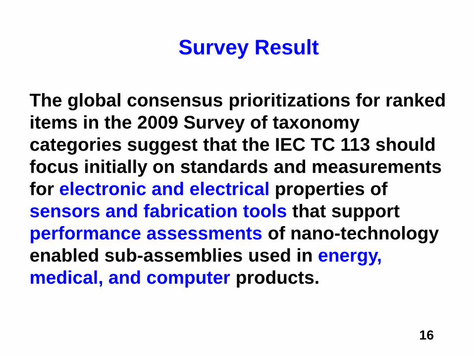
16
The global consensus prioritizations for ranked items in the 2009 Survey of taxonomy categories suggest that the IEC TC 113 should focus initially on standards and measurements for electronic and electrical properties of sensors and fabrication tools that support performance assessments of nano-technology enabled sub-assemblies used in energy, medical, and computer products.
Survey Result

17
IEC/TC 113 Published StandardsIEC/IEEE 62624: Test methods for measurement of electrical properties of carbon nanotubes (First published by IEEE-SA in 2005; now in maintenance cycle under IEC/IEEE dual logo).
Examples of IEC/TC 113 Projects in ProgressIEC/IEEE Technical Specifications 62659, Large scale manufacturing of nanoelectronics. This is an approved new work item. Development work will begin in 2010.IEC/IEEE 62xxx, Technical Report for the TC 113 on nanoelectronicsstandardization roadmap. Begins in 2010.IEC 62xxx, Technical Report on nanoscale electrical contacts and interconnects. Development work will begin in 2010.
A benzene molecule junction spans platinum atomic point contacts.Figure from L. Venkataraman, Viewpoint – Benzene provides the missing link in molecular junctions, Physics 1, 5 (2008) at http://physics.aps.org/articles/v1/5 http://dx.doi.org/10.1103/Physics.1.5 Reprinted with American Physical Society permission from Physics, 1, 5 (2008); illustration by Alan Stonebraker.

18
ISO TC 229 on nanotechnologiesEstablished in 2005.
ScopeThe scope of ISO TC 229 is standardization for nanotechnologies that includes either or both of the following:
1. Understanding and control of matter and processes at the nanoscale, typically, but not exclusively, below 100 nonameters in one or more dimensions where the onset of size-dependent phenomena usually enables novel applications and
2. Utilizing the properties of nanoscale materials that differ from the properties of individual atoms, molecules, and bulk matter, to create improved materials, devices, and systems that exploit these new properties.

19
Scope (continued)
Specific tasks include developing standards for: terminology and nomenclature; metrology and instrumentation, including specifications for reference materials; test methodologies; modeling and simulations; and science-based health, safety, and environmental practices.

20
ISO TC 229 Working Groups
• JWG 1: Terminology and Nomenclature
• JWG 2: Measurement and CharacterizationJWG 1/JWG 2 are Joint Working Groups with IEC TC 113• WG 3: Health, Safety and Environmental (HSE) Aspects of NanotechnologiesScope: The development of science-based standards in HSE aspects of nanotechnologies. A key part of the strategy for WG3 is to develop a framework and roadmap. There are high-priority needs for standard methods for toxological screening, toxicity/hazard potential determinations, occupational exposure limits, etc. for nanoparticulates and other nanoscale materials; and protocols for inhalation testing, toxicology testing, safe handling, exposure determination and safe disposal of nanotubes.

21
ISO TC 229 Working Groups (continued)
• WG 4: Material specifications Scope: (work in progress) The development of material specifications for about 40 distinct materials and four classes of materials. These include metallic nanoparticles, such as gold, silver and platinum; metal oxides nanoparticles such as zinc and titanium oxides; compound particles such as polymers and alloys; and functionalized nanoparticles and quantum dots. Works in closed collaboration with JWG2 to ensure coordination of measurement, characterization and test methods.

22
The Diffuse TC113/TC229 Moving BoundaryTerms of Reference for
IEC TC 113 WG3 on Performance Assessment
IEC TC 113 WG3 -- MARKET PULL
Nano Product AttributesPerformanceReliabilityDurability (end-of-use)Disposing and Recycling (end-of-life)
Diffuse Moving Boundary
ISO TC 229 JWG2 -- TECHNOLOGY PUSH
IEC TC 113
Nanotechnology moving towards innovative commercialization
Work-in-Progress DRAFT - Subject to change.

23
Common Theme Among Recent Workshops on Nanotechnologies and NanoManufactruring#
• Limited resources and knowledge for developing the critical science- and engineering-based metrology.
• Support for all sages of the economic and materials cycles from research to recycling and eventual disposal.
• Challenges are :- Characterizing, understanding, mdoeling, and controlling the
key properties and processing parameters of nanomaterials.- Assessing the performance (figures of merit) of products
that have added value and functionalities enabled by nanotechnologies.
# See for example, http://www.nist.gov/cstl/upload/nano_small_web-4.pdf

24
Opportunities for Additional Collaborations
Are more than Moore applications of electronics appropriate now for international standards and metrology efforts?
Will the past business models for standards and metrology in support of the semiconductor industry be optimum for the diverse applications of nanotechnologies?
From where will the essential resources come?
25
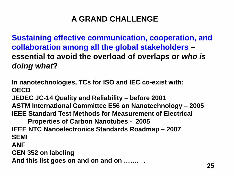
A GRAND CHALLENGE
Sustaining effective communication, cooperation, and collaboration among all the global stakeholders –essential to avoid the overload of overlaps or who is doing what?
In nanotechnologies, TCs for ISO and IEC co-exist with:OECD JEDEC JC-14 Quality and Reliability – before 2001ASTM International Committee E56 on Nanotechnology – 2005IEEE Standard Test Methods for Measurement of Electrical
Properties of Carbon Nanotubes - 2005IEEE NTC Nanoelectronics Standards Roadmap – 2007SEMIANFCEN 352 on labelingAnd this list goes on and on and on ……. .
26
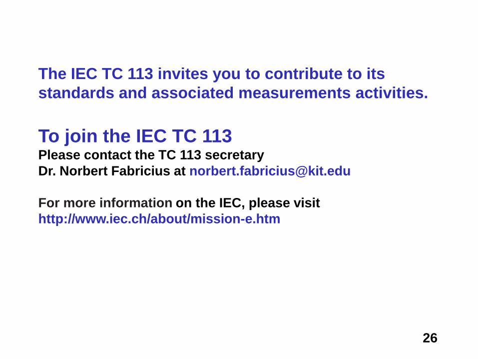
The IEC TC 113 invites you to contribute to its standards and associated measurements activities.
To join the IEC TC 113Please contact the TC 113 secretaryDr. Norbert Fabricius at [email protected]
For more information on the IEC, please visit http://www.iec.ch/about/mission-e.htm

27
THANK YOU