glove drummer - ucf department of eecs · glove drummer aims to provide an intuitive,...
TRANSCRIPT
Glove Drummer MIDI Controller and Audio Playback Module
Group 15:
Aaron Rice
Michael Moran
Timothy Cox
Group 15
i
Glove Drummer
Table of Contents
Table of Contents .................................................................................................. i
1.0 Executive Summary ........................................................................................ 1
2.0 Project Definition ............................................................................................ 1
2.1 Personnel .................................................................................................... 2
2.2 Goals & Objectives ..................................................................................... 2
2.3 Requirements and Specifications ................................................................ 3
2.3.1 Hand Modules ...................................................................................... 3
2.3.2 Tabletop Module ................................................................................... 4
2.3.2 Pedal Sensors ...................................................................................... 5
3.0 Research ........................................................................................................ 6
3.1 Musical Instrument Digital Interface (MIDI) ................................................. 6
3.2 Electronic Drum Kits ................................................................................... 8
3.2.1 Electronic Drum Pads and Cymbals ..................................................... 8
3.2.2 The Drum Brain .................................................................................... 8
3.3 Glove Controllers ...................................................................................... 12
3.3.1 Musical Glove Controllers ................................................................... 12
3.3.2 Other Glove Controllers ...................................................................... 12
3.4 Serial Communications ............................................................................. 13
3.4.1 The UART and RS-232 Protocol ........................................................ 13
3.4.2 The USART and Synchronous Half-Duplex Serial Protocol ............... 15
3.5 Digital Audio .............................................................................................. 15
3.5.1 Recording Digital Audio ...................................................................... 17
3.5.2 Playback of Digital Audio .................................................................... 18
3.6 Using an SD Card in Embedded Projects ................................................. 21
3.7 Wireless Communication .......................................................................... 22
3.7.1 Available Technologies and Devices .................................................. 22
4.0 Design .......................................................................................................... 22
4.1 Hardware .................................................................................................. 22
Group 15
ii
4.1.1 Microcontroller Development Boards.................................................. 22
4.1.2 FPGA Development Board: The Spartan X3CS500E Core Board ..... 25
4.1.3 UART to PC Interfaces ....................................................................... 26
4.1.4 Connection Between Left/ Right Hand Modules and Table-top Module .................................................................................................................... 27
4.1.5 SD Card .............................................................................................. 29
4.1.6 Supplying Power ................................................................................ 33
4.1.7 Hardware for Expanded Mapping Flexibility and Hi Hat Control ......... 36
4.1.8 Level Shifter Circuits........................................................................... 38
4.1.9 ADCs .................................................................................................. 39
4.1.10 The Vishay DG Multiplexer ............................................................... 41
4.2 Software .................................................................................................... 44
4.2.1 C Code Programs ............................................................................... 44
4.2.2 Energia Code for Tiva C series .......................................................... 48
4.2.3 Verilog Code for the Spartan FPGA ................................................... 55
4.2.4 Hex Editor Software............................................................................ 58
4.2.5 Audacity Digital Audio Workstation (DAW) ......................................... 60
4.2.6 BFD3 Drum Software ......................................................................... 60
4.2.7 WAV2C Software ............................................................................... 61
4.2.8 Hairless Serial to MIDI Software ......................................................... 61
4.2.9 LoopMIDI Software ............................................................................. 62
5.0 Prototyping ................................................................................................... 63
5.1 Construction of Piezo Sensors .................................................................. 63
5.2 Construction of the Gloves ........................................................................ 64
5.3 Construction of the Hi Hat Pedal ............................................................... 64
5.4 Construction of the Bass Drum Pedal ....................................................... 65
5.5 Left/ Right Hand Module in the Breadboard Phase ................................... 65
5.6 Table-top Module in the Breadboard Phase.............................................. 66
5.6.1 Sub-Modules ...................................................................................... 67
6.0 Piezo Signal Conditioning ............................................................................. 70
6.1 The Unconditioned Piezo Signal ............................................................... 70
6.2 The Piezo Conditioning Circuit .................................................................. 72
6.2.1 Op Amp Selection .............................................................................. 72
6.2.2 Bounding the Piezo Signal between Ground and Vcc ........................ 73
6.2.4 The Final Conditioning Circuit Design ................................................ 74

Group 15
iii
7.0 PCB Planning ............................................................................................... 75
7.1 Signal Integrity .......................................................................................... 76
7.2 Custom PCB for Left/ Right hand Modules ............................................... 77
7.2.1 Power Supply ..................................................................................... 77
7.2.3 Integrated Circuits (ICs) ...................................................................... 77
7.2.4 Clock Circuits ..................................................................................... 80
7.2.5 Programming Interfaces ..................................................................... 81
7.2.6 Bill of Materials (BoM) ........................................................................ 82
7.2.7 Complete Hand Module PCB Schematic ............................................ 85
8.0 Assessing Latency and Jitter ........................................................................ 87
9.0 Administrative Content ................................................................................. 87
9.1 Milestone Discussion ................................................................................ 87
9.2 Budget and Finance .................................................................................. 88
10.0 Conclusions ................................................................................................ 89
Appendix: References ........................................................................................ 90
Group 15
1
1.0 Executive Summary
With Glove Drummer, the power of music is in the palm of your hand. The Glove Drummer team would like to thank Ray K. and Guitar Center for allowing the research of modern electronic drum sets at their Winter Park location. Electronic Drum sets have been around for 40 years or more, and have already evolved to closely mimic the nuances of acoustic drums. However, these electronic drum sets are equally, and unnecessarily, as large and clunky as their acoustic counterparts. Glove Drummer aims to intuitively map an electronic drum kit to a pair of pair of gloves, replacing the need for large and immobile drum kits. By utilizing a pair of drum gloves, two pedal sensors, and a table-top module, Glove Drummer will provide the user with all the same interfacing and customizability already found in modern electronic drum kits. While an intuitive default will be present, users will be able to completely customize Glove Drummer with their own personal set of drum sounds. Also, computer connectivity will allow to the user to utilize the same Digital Audio Workstations they are already familiar with. The left and right hand modules of Glove Drummer will feature velocity sensitive sensors, allowing the user to play a full drum kit on any hard surface. By utilizing velocity sensitive sensors, Glove Drummer will closely mimic the different acoustics associated with striking a drum kit at varying velocities. The hand modules will transmit this information wirelessly to the table-top module. The pedal sensors, which are wired to the table-top module will allow the user to control the hi-hat and play the bass drum in the same manner they are already accustomed to. The table-top module will then generate sound samples based on the messages sent by the hand modules and pedal sensors. The table-top module will utilize an SD card to store the library of sound samples, allowing the user to load their personal library onto a small card, or use multiple cards for easy swapping of audio sample libraries. Electronic drum users will greatly appreciate the mobility provided by Glove Drummer. By eliminating the large drums and pieces associated with a standard drum kit, Glove Drummer can easily be transported wherever a band intends to play, without requiring a vehicle sometimes as large as a mini-van just to house their drums. Also, as Glove Drummer can be played on any hard surface, areas as small as office cubicles can suddenly be used to practice and write music.
2.0 Project Definition
Group 15
2
2.1 Personnel Aaron Rice- Electrical Engineering
Timothy Cox- Computer Engineering
Michael Moran- Electrical Engineering
2.2 Goals & Objectives Glove Drummer aims to provide an intuitive, user-friendly, compact, and mobile alternative to the modern electronic drum kit. The hand modules will allow the user to play Glove Drummer on any hard surface. Utilizing intuitive sensor mapping, Glove Drummer will be an easy transition for any advanced drum player, while also being approachable to new users interested in electronic drums. One major goal of Glove Drummer is ease of use. To this end, the gloves will be comfortable and must not restrict freedom of motion. Also, the gloves will be intuitive enough that experienced electronic drum users will have an easy time making the transition to Glove Drummer, but will be simple enough to allow new users to simply put on the gloves and play. By utilizing a compact table-top module, Glove Drummer will be portable enough to take anywhere, and can turn any space into a music studio. Another major goal of Glove Drummer is versatility. One way this will be achieved is allowing users to load their own personal audio library for use. Although Glove Drummer is designed to be a replacement for electronic drum kits, the user can make it play any sounds they desire, allowing Glove Drummer to be used as any instrument the user wishes, be it a piano, trumpet, etc. The ability to quickly swap SD cards and load new audio files will allow the user to switch between Glove Drummer functionalities in an instant. Also, by utilizing a USB connection and the same MIDI messages found in other electronic drum kits, Glove Drummer will be able to work with the same Digital Audio Workstations that experienced electronic drum users will already be familiar with. A third major goal of Glove Drummer is accuracy of emulation. This means that Glove Drummer must closely mimic the sounds of a standard drum kit. To this end, the sensors in the left/right hand modules must be velocity sensitive, to mimic loud and soft hits on a drum kit. The bass pedal must also utilize a velocity sensitive sensor, for the same reason. The hi-hat pedal will function much like a standard hi-hat pedal. Depressing the hi-hat pedal partially will cause the hi-hat sensor on the hand modules to make sounds corresponding with partially closed hi-hat. Fully
Group 15
3
depressing the hi-hat pedal will close the virtual hi-hat, and not pressing it at all will open it. Also, for emulation accuracy, quickly opening or closing the hi-hat will produce its own unique sound. In addition, the tabletop module must be able to read sensor information and playback audio with low latency, specifically under 15ms.
2.3 Requirements and Specifications Glove Drummer will be split up into three major components, the Left/Right Hand Modules, the Tabletop Module, and the pedals. The requirements and specifications for each is found below.
2.3.1 Hand Modules The left/right hand modules have several strict requirements to allow for practical playability. Outlined in table 1, these requirements ensure that Glove Drummer will possess ease of use, and will properly mimic a standard drum kit. Table 1: Hand Module Requirements
Overall Component Requirements
1. The Glove Drummer hand modules must not weigh over two pounds, and must be securely fastened to users hands via wrist straps
2. The hand modules must be powered by battery
3. The hand modules must use low power components, to extend battery life
4. The hand modules must communicate with the tabletop unit wirelessly
5. The hand modules must be comfortable to play extended sessions
6. The hand modules must be flexible enough as to not restrict finger or hand motion
7. The hand modules must utilize velocity sensitive sensors to closely mimic an acoustic drum kit
8. The hand modules must have one velocity sensitive sensor per finger, as well as one on the palm
9. The hand modules must be intuitively mapped to a standard drum kit
Group 15
4
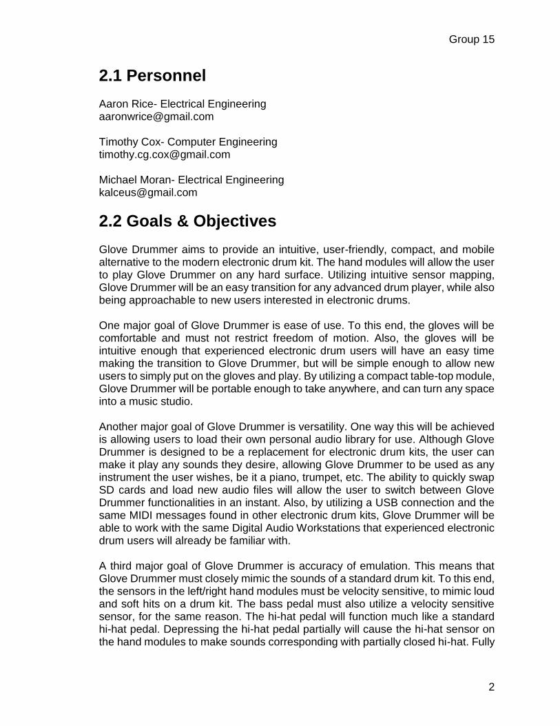
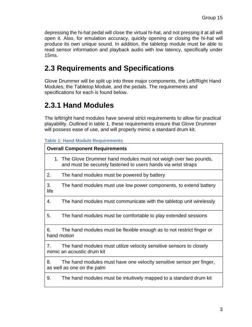
While Glove Drummer will allow the user to load their preferred audio files, and match them with any sensor of their choosing, Glove Drummer will have an intuitive standard mapping, as shown below in figure 1. Exact sensor location, and means of fastening the hand modules, are better depicted in figure 2.
Figure 1: One possible sensor to drum sound mapping
Figure 2: Hand and Tabletop Modules
2.3.2 Tabletop Module The tabletop module has several strict performance requirements in order to emulate a standard drum kit. Listed below in table 2, these requirements will
Group 15
5
ensure that Glove Drummer can’t be distinguished from a standard drum kit by sound alone. Table 2: Table-top Module Requirements
Overall Component Requirements
1. The tabletop module must fit on a standard sized desk or table
2. The tabletop module must receive input from hand and pedal modules, and correctly play the corresponding audio file
3. The tabletop module must mix audio files without changing the total volume
4. The tabletop module must play audio files with less than 15ms of latency between sensor input and audio output
5. The tabletop module must playback audio through an onboard speaker
6. The tabletop module must possess a standard 3.5mm headphone jack
7. The tabletop module must possess computer connectivity via USB
8. The tabletop module must utilize an interchangeable SD card for audio file storage
9. The tabletop module must utilize MIDI messaging to interact with existing digital audio software
10. The tabletop module must possess a master volume switch
2.3.2 Pedal Sensors Glove Drummer will utilize two different pedal sensors in order to emulate a standard drum kit, a hi-hat pedal and a bass pedal. The requirements for each of these pedals are different, and are listed below in table 3.
Table 3: Bass and Hi-Hat Pedal Requirements
Overall Component Requirements
1. The hi-hat pedal must detect the level to which it is currently depressed
2. Quickly pressing or releasing the hi-hat pedal must generate its own unique audio playback sample
Group 15
6
3. Both the bass and hi-hat pedals must be of comparable size to standard drum pedals
4. The bass pedal must possess a velocity sensitive sensor
5. Both the bass and hi-hat pedals must communicate with the tabletop module via wired communication
3.0 Research
3.1 Musical Instrument Digital Interface (MIDI) MIDI was created in 1983 (source1) and is associated by some with the music from a Nintendo or other early gaming system. This could not be further from the truth. MIDI does not represent any certain type of sound, only commands to create and alter sounds. Synthesized sounds stored in tables were initially used in the past, resulting in that “Nintendo sound,” and therefore that association was made. The processing power and data storage capacity of microcontrollers around the time of MIDI’s invention just did not allow for actual recorded audio tracks to be triggered by MIDI controller devices. Today you will find MIDI being used for light shows, synthesized sounds, and the playback of actual recorded audio tracks. The Glove Drummer left and right hand modules will serve as MIDI controllers whereas the table-top module will serve as a MIDI sequencer. MIDI controllers interpret data from the outside world and create messages. MIDI sequencers decode the messages from the MIDI controller and produce sounds. Although the sequencer is sometimes called a “MIDI synthesizer” it should be noted that the sounds produced could be synthesized or acoustic depending on the user’s preference. Glove Drummer will feature an onboard MIDI synthesizer, but also will give the option of using a PC software as the MIDI synthesizer. Drum software like BFD3 will no doubt produce the most realistic drum sounds when compared to the sounds produced by the table-top module as most electronic drummers prefer these sounds to the sounds produced by their professional electronic drum sets. The communication protocol that is MIDI dictates that each message contains three bytes. The first byte is called the status byte and tells what type of message is being sent and on what channel. The channel information can be one of 16 values and drums are reserved for channel nine in the MIDI specification. The type of message is found in the upper half (or nibble) of the status byte. Types of messages important in implementing Glove Drummer will be limited to Note On, Note Off, and Continuous Control (CC). Other types of messages may have an important function when trying to mimic other instruments, but are mostly useless in the case of drums. A type of message called “after touch” has been used in some electronic drum sets, but CC messages can achieve the same results.

Group 15
7
The second of three bytes (data1) in a message contains the “key,” since MIDI was designed based around the musical keyboard. For the purpose of electronic drum sets, key can be thought of as whatever drum the message is intended trigger. There are 128 keys equivalent to a 7-bit value, meaning the Most Significant bit (MSb) is always zero. The same goes for the third byte of the message. This could be used as a way to differentiate between the status byte and data bytes, because the status byte will always have an MSb equal to one. The third and final byte in a message (data2) contains “velocity” information. Velocity information equates to how hard the drum or cymbal was struck. Since the MSb of data2 is always zero, there are 128 possible values for velocity where velocity=0 produces no sounds. When an acoustic drum is struck with varying force, the sounds produced differ not only in volume, but also in timbre. This is the reason electronic drum sets store audio tracks of each drum being hit with varying force or velocity. In Figure 3 below, the messages needed to produce a single drum sound are shown. Two three byte messages are needed in order to turn the sound on and then turn it off. The Note Off message does not actually turn any note or sound off, but it is required to play the next sound for that “key” or particular drum. It could be said that when a MIDI synthesizer is configured to play drum sounds that the Note Off message is ignored. Note Off has an important role in creating other musical instrument sounds, but not in creating drum sounds.
Figure 3: Standard six byte Note On/Off Combo message for drum strike
Another method called “running status” only requires that the second message contain two bytes as the status of the first message is perceived also as the status of the second message. A message using running status can be seen below in Figure 4. This is possible because the second message is also a Note On message for channel nine, but the velocity information in data2=0x00 effectively turns off the sound. Any additional Note On messages on channel nine may also omit their status bytes so long as no CC messages were generated in the interim period. This method saves time and therefore reduces potential latency. For this reason, the running status method will be implemented in Glove Drummer.
Figure 4: Note On/Off combo using running status

Group 15
8
3.2 Electronic Drum Kits Forty-four years ago the first electronic drum kit was created for Graeme Edge of the band Moody Blues (source2). Since that time great improvements have been made to electronic drums such as variable hi hat control, positional and cymbals, and the replacement of synthesized sounds with recordings of real sounds.
3.2.1 Electronic Drum Pads and Cymbals The Drum pads and cymbals all have one or more piezoelectric disc transducers embedded somewhere within them, protected by foam or foam rubber. Some drums like the toms have only one, whereas the hi hat and snare sometimes have two for judging the position where the stick hit the hi hat or snare. The hi hat cymbal is also controlled by the hi hat pedal. Electronic hi hat pedals work in one of two ways. The more primitive way uses discrete open hi hat and closed hi hat positions. A better approach is called variable hi hat control which records the position of the pedal between open and closed so that the sounds created are more natural when compared to the sound of an acoustic hi hat. An acoustic ride cymbal can make three different distinct sounds and accordingly some of the better electronic ride cymbals include three transducers for recreating this effect. Another feature in some cymbals is the ability to strike the cymbal and quickly “choke” it by grabbing the edge between the thumb and fingers. In this case a sensor, which may not be a piezo disk, is placed near the edge of the cymbal to sense the cymbal has been “choked.” All of these features have been designed in order to make electronic drums more attractive to drummers. In the following section the team explores the MIDI messages created by Roland’s flagship electronic drum set which includes all of the features mentioned here.
3.2.2 The Drum Brain Early during Senior Design I, the team took a trip to Guitar Center, a music store in Winter Park, where the inner workings of the Roland TD-30 electronic drum set were explored. The Roland TD-30 is arguably the best electronic drum set there is with many features that help to make it respond close to the way an acoustic drum set would. The “drum brain” has input jacks for each of the sensors found throughout the drums, cymbals, and hi hat pedal. It takes the signals from those sensors and plays pre-recorded drum sounds through an audio output jack. Surprisingly, many electronic drum players choose to record their kits using other pre-recorded sounds from computer software and not the sounds stored in the drum brain. This choice is usually made because the user feels that the sound libraries offered by computer software are of superior quality when compared to the drums brain sound library. The team could only conclude from the preferences of electronic drum users that the MIDI messages sent from a drum brain include all the necessary data to trigger drum sounds in a way that effectively emulates an acoustic drum set. Knowing this, the team studied the output of MIDI messages
Group 15
9
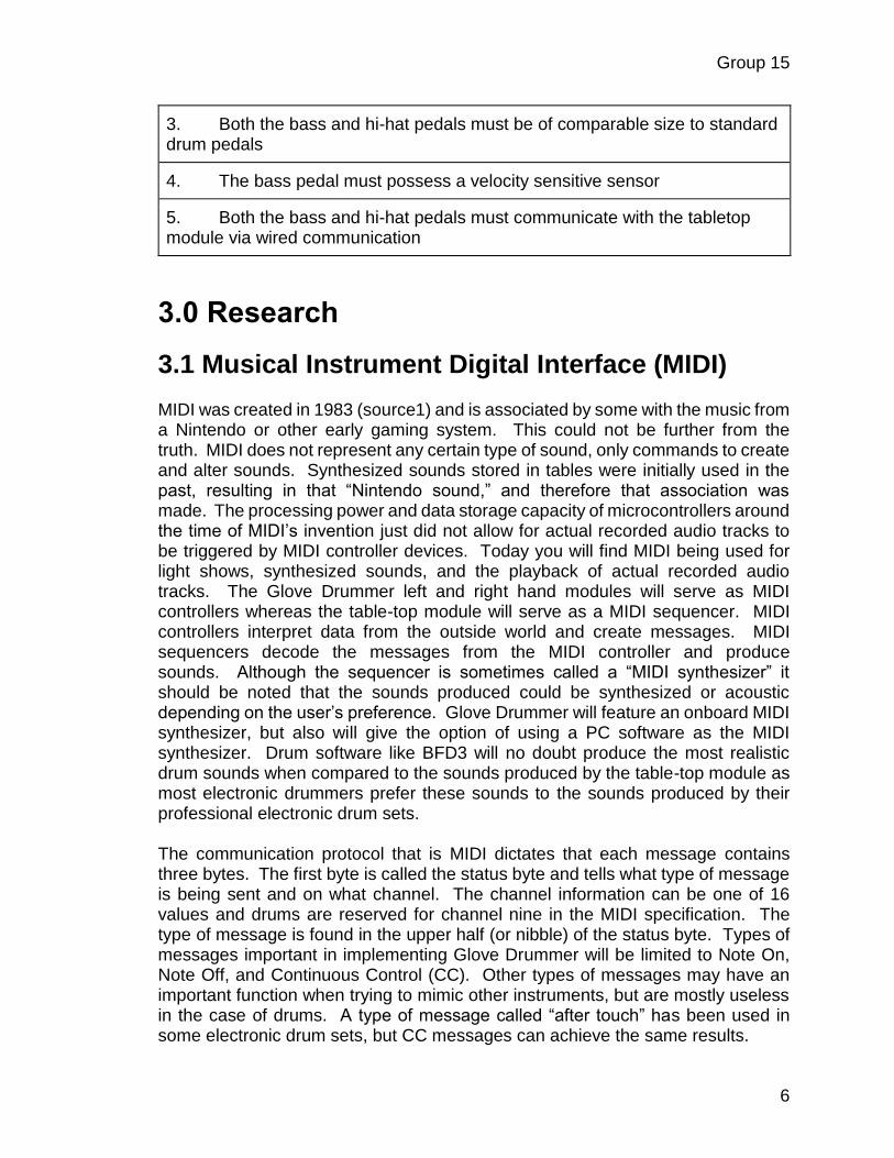
from the TD-30 drum brain in an attempt to understand exactly what data is needed by the drum software and why. The MIDI output of the TD-30 was connected to a laptop PC through MIDI/USB interface. A program called “MIDI Ox” was used to record the MIDI messages as they were created. Screenshots from MIDI Ox are shown and explained below.
Figure 5: TD-30 Drum Brain - MIDI output for positional snare drum
In Figure 5 shown above, a positional snare drum is hit in the center of the drum and then on the rim of the snare (the outer perimeter) of the drum. This progression from center to rim is repeated three times. A “positional snare” is nothing more than an electronic drum with two piezo sensors, one placed in the center of the drum and one closer to or on the rim. They are made this way because an acoustic snare drum will sound different depending on how close to the center it is struck. In Figure 5 above, the MIDI messages reveal that a Continuous Control (CC) message precedes each “Note On/ Off combo.” Data3 of the CC message is the data that would tell the drum software how close to the rim the snare was struck. Like velocity data, CC data3 is a 7 bit value where 0x7F corresponds to the snare being struck directly on the rim while 0x00 corresponds to the snare being struck directly in the center of the drum. Values in between of course correspond the snare being struck somewhere in between the center and the rim. For software that may only have sounds for the center and rim position that does not use CC messages, data2 of the note on/off combo is different. It is reasonable to assume that this change in data2 is made as the stick crosses the radial line halfway between the center and the rim. The concept of a positional snare could be implemented in Glove Drummer by placing a sensor on the fingertip and another lower on the finger, palm-side, corresponding to the center and rim sensors of a positional snare drum. Most likely only discrete center or rim messages could be discerned, although cross-talk between the two sensors resulting from the fact they are both attached to the same finger might allow for CC messages to be sent with positional values between the center and rim.
Group 15
10
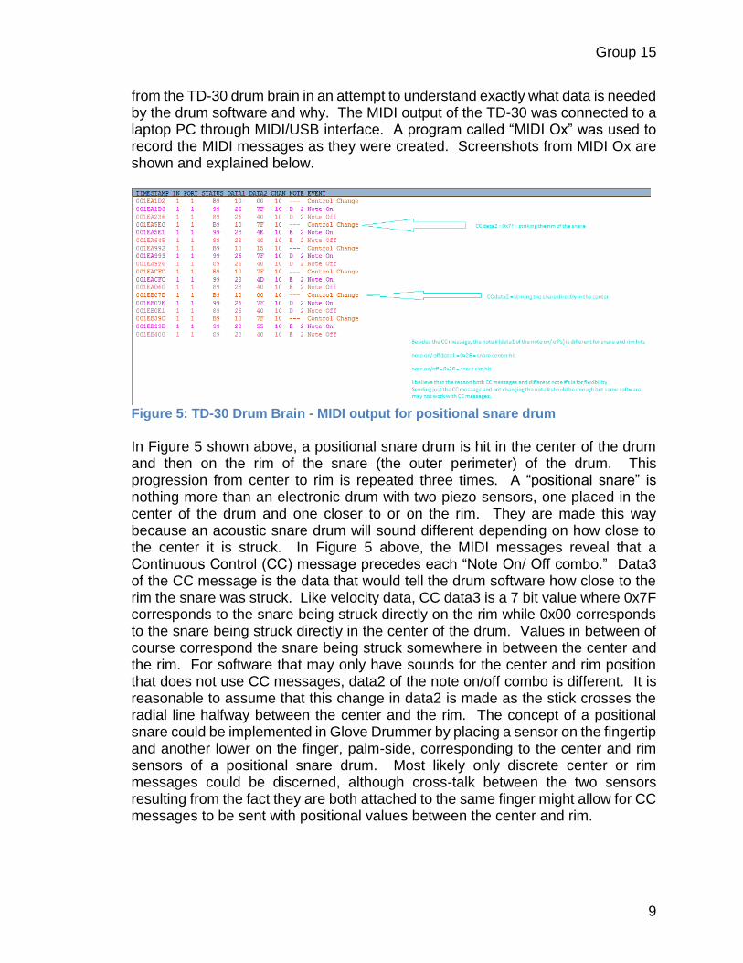
Figure 6: TD-30 Drum Brain - MIDI output for hi hat struck on bow then edge
In Figure 6 above, MIDI messages are shown resulting from striking the positional hi hat on the bow (halfway between the center and perimeter of the cymbal, struck with the tip of the stick) and then the edge (perimeter of the cymbal struck with the shank of the stick). This progression from bow to edge is repeated three times, each time with the hi hat pedal fully open. As with the positional snare, a CC message precedes each note on/off combo except that here it is the position of the hi hat pedal between open and closed that is contained in data2 of the CC message. As shown above, CC data2 for the hi hat pedal is 0x00 for the fully open position. The position where the stick struck the hi hat cymbal is given discretely as either bow or edge and nowhere in between. This information is contained in data1 of the note on/off combo and can be seen to alternate between 0x2E = bow hit and 0x1A = edge hit. Glove Drummer will also feature a variable hi hat pedal which provides a seven bit range of values between open and closed. Bow/ edge hi hat hits could also be implemented as previously mentioned with the positional snare drum. In Figure 7 below, a sound created solely by movement of the hi hat pedal called the “foot chick” sound is produced by the TD-30 drum brain. As the hi hat pedal moves quickly toward the floor, CC data2 increases from 0x00 to 0x5A. Interestingly, the hi hat pedal when fully depressed reads a value of 0x5A and not 0x7F (the max 7-bit value it could be). When implementing the Glove Drummer hi hat pedal, the team reasons that values from open to closed read from the pedal sensor need not range all the way from 0x00 to 0x7F. When the pedal reaches the fully depressed position, a note on message is sent the MIDI sequencer to play the foot chick sound. Note off messages were thought be to be ignored in all cases by the MIDI sequencer and after careful analysis of the time step in the leftmost column, this assumption was correct. Subtracting the note on time from the note off time for all cases resulted in 99 to 100 time steps between note on and note off. The time step is believed to be the inverse of the MIDI baud rate of 31250bps = 32us. One hundred of those time steps equals only 3.2ms, much too short to be able to hear the full response of a drum hit which usually lasts around 3s.
Group 15
11
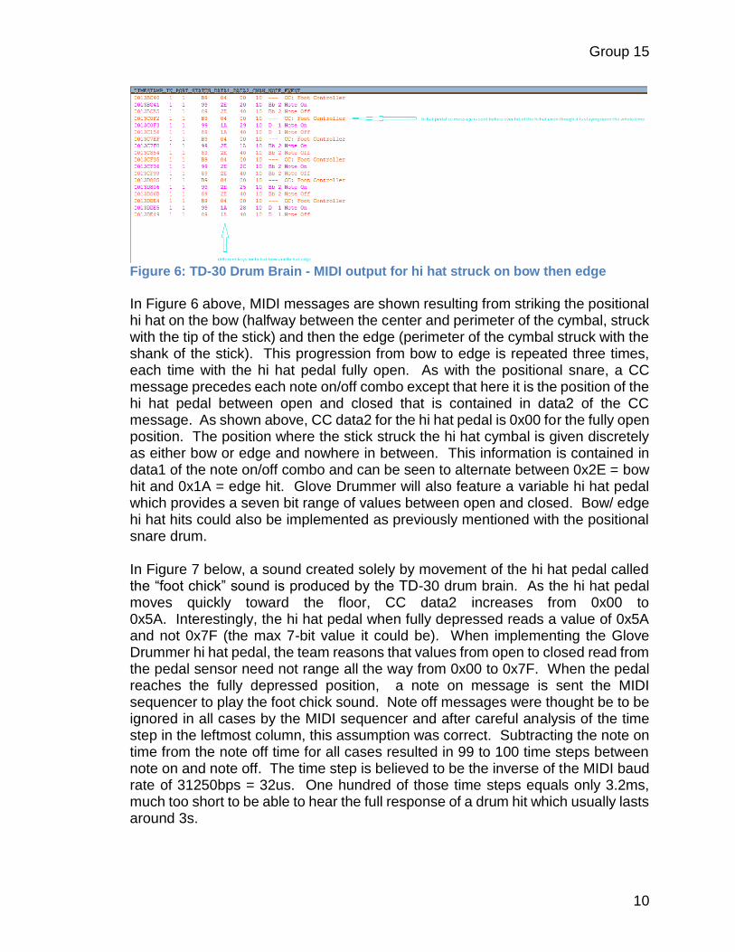
Figure 7: TD-30 Drum Brain - MIDI output for hi hat “foot chick” sound
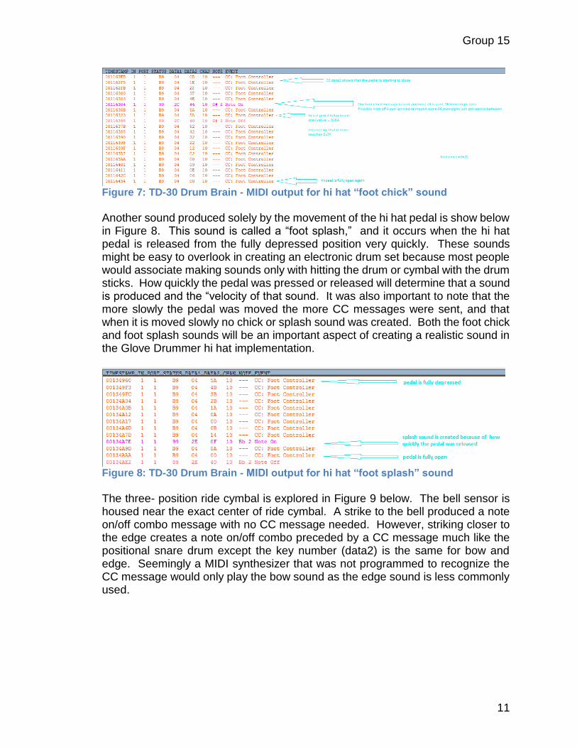
Another sound produced solely by the movement of the hi hat pedal is show below in Figure 8. This sound is called a “foot splash,” and it occurs when the hi hat pedal is released from the fully depressed position very quickly. These sounds might be easy to overlook in creating an electronic drum set because most people would associate making sounds only with hitting the drum or cymbal with the drum sticks. How quickly the pedal was pressed or released will determine that a sound is produced and the “velocity of that sound. It was also important to note that the more slowly the pedal was moved the more CC messages were sent, and that when it is moved slowly no chick or splash sound was created. Both the foot chick and foot splash sounds will be an important aspect of creating a realistic sound in the Glove Drummer hi hat implementation.
Figure 8: TD-30 Drum Brain - MIDI output for hi hat “foot splash” sound
The three- position ride cymbal is explored in Figure 9 below. The bell sensor is housed near the exact center of ride cymbal. A strike to the bell produced a note on/off combo message with no CC message needed. However, striking closer to the edge creates a note on/off combo preceded by a CC message much like the positional snare drum except the key number (data2) is the same for bow and edge. Seemingly a MIDI synthesizer that was not programmed to recognize the CC message would only play the bow sound as the edge sound is less commonly used.

Group 15
12
Figure 9: TD-30 Drum Brain - MIDI output for ride cymbal struck on the bell, then bow, then edge
It is unclear at this point how many of the features may be able to be incorporated into a glove controller. With the exception that the bounce of a drum stick off the drum head is not possible with the fingers, Glove Drummers design will basically be a mapping of an electronic drum set to a pair of gloves. The team believes simple not on/off messages created by the tiny 9.5mm piezos will work nicely for producing velocity sensitive drum sounds. Additionally the team believes that with the use of infrared (IR) proximity sensors a variable hi hat control pedal should possible. Getting a chance to view these messages from the TD-30 was of great benefit to the team in understanding how Glove Drummer will be designed and programmed.
3.3 Glove Controllers
3.3.1 Musical Glove Controllers There are notably few instrumental glove controllers available for comparison and none readily available commercially. Existing instrumental glove controllers generally feature wired hand modules and poor customizability. Many models utilize one volume fits all drum sounds, which does a poor job mimic the acoustic finesse of an actual drum kit. By allowing users to connect Glove Drummer to existing digital audio workstations, such as Audacity, and utilizing piezoelectric sensors, Glove Drummer will better mimic standard acoustic drum kits, whilst providing the customizability associated with modern electronic drum kits. Utilizing wireless communication, Glove Drummer will also offer the user greatly enhanced freedom of motion.
3.3.2 Other Glove Controllers Whilst very few instrumental glove controllers have been developed, glove controllers have been developed for a large array of applications. As early as 1989, the Nintendo power glove combined a wearable glove with control features. Touch activated sensors and accelerometers are inputs present in most glove control applications. However, one specification that is of extreme importance to any glove controller is freedom of motion. By utilizing only small piezoelectric sensors, Glove Drummer is at an advantage in this regards. And while the presence of Lithium Ion
Group 15
13
batteries and a wireless component will increase the size of the Glove Drummer hand modules, the lack of an attached cord removes many limitations associated with most glove controllers.
3.4 Serial Communications Communication between MCUs generally is done bit by bit, or serially, so that less pins on either MCU are used versus using parallel communication. Data lines are usually held high in their idle state which is a practice used ever since the telegraph (source3). Keeping data lines high allows the receiving device to determine if the transmitting device is functioning. If the receiving device were to receive zero volts at all times, the assumption could be made that the transmitting device was not functioning. Serial communications can be either asynchronous or synchronous. In asynchronous communications the sender and receiver must agree on the speed of transmission, or baud rate, as there is no clock line between the two devices. Because there is no clock line, asynchronous communication has a maximum speed of about 115,200 bps. Synchronous communications however uses a clock lines between devices and can attain much faster speeds. Implementing Glove Drummer will require communication between devices and serial communication will be required given the toal number of pins available on these devices. Initially Glove Drummer will use asynchronous communication between devices. If the team encounters latency issues, using synchronous communication in order to make each transmission faster may be required.
3.4.1 The UART and RS-232 Protocol Since our project will rely heavily on smooth communication with our embedded systems it is important for us to review and refresh ourselves with how UART (universal asynchronous receiver/transmitter) works and how it works well with the RS-232 Protocol. The RS-232 serial communication protocol is a standard protocol that was designed for asynchronous communication. To understand how it will work for us the team will setup a situation that will be very similar to what our glove drummer project will entail. Suppose we have our Tiva C communicating with another UART based device via a serial link. The team needs to implement a serial data transmission and the RS-232 protocol can really help with this. The hardware configuration begin discussed is shown in the figure below..

Group 15
14
Figure 10: UART hardware configuration
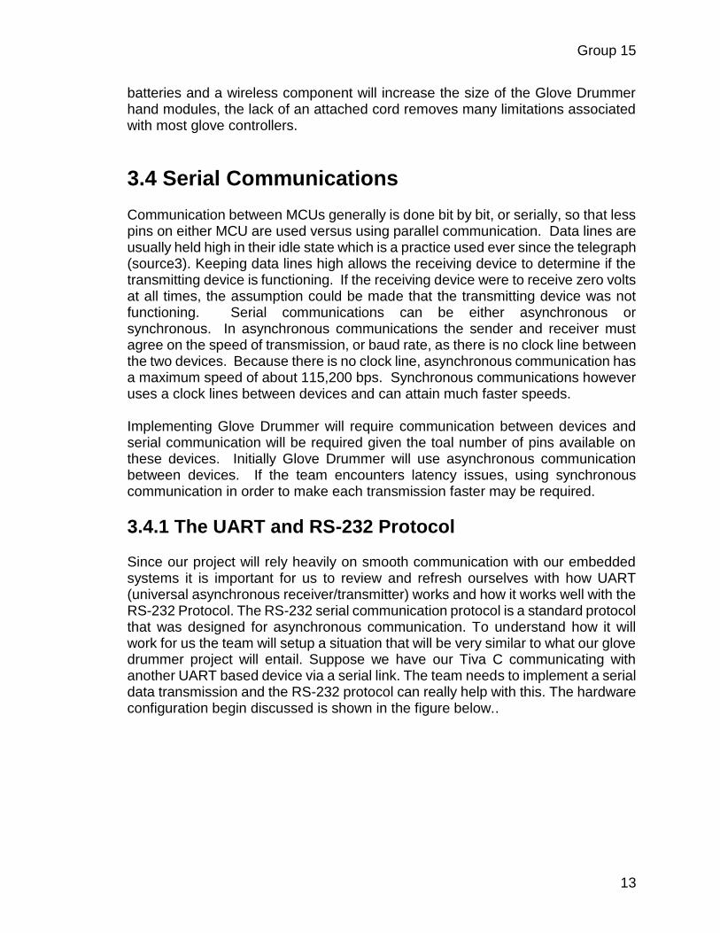
The UART sits between the host computer and the serial channel. The serial channel is the collection of cables over which the bits are transmitted. The output from the UART is a standard range of 0 or 5 volts. The standard sets voltage levels that go hand in hand to logical on and logical zero levels for not only data transmission but for the control signal lines as well. Signals range from +3 to +15 volts. For our project the team will most likely want to stick to 0 to 5 volts. Because both ends of the RS-232 circuit depend on the ground pin being zero volts, issues will occur when connecting embedded computers where the voltage between the ground pin on one end, and the ground pin on the other is not zero. This may also cause a hazardous ground loop. To avoid this in our project the team will have to make not of all the control signals tied in with the RS-232 protocol. A small descriptive chart I found in Figure () will help a lot with referencing the signals when working on our final project. The team should also note RS-232 devices may be classified as Data Terminal Equipment (DTE) or Data Communication Equipment (DCE). DCE is what the team will use to wire send and receive the signals with our Tiva C or maybe even our FPGA device. Just to note for reference the team will most likely use a 3-wire connection in RS-232, one to receive, transmit data, and ground. In order to optimize bandwidth, reduce noise, and increase range, this TTL logical level is converted to an RS-232 logic level because it can handle that data a lot better since it was made for asynchronous communication. The data frame in the RS-232 Protocol consists of a start bit, seven data its, and the parity bit and two stop bits. The parity bit here is the core functionality of the protocol, trying to detect potential transmission errors. This will give us a flag anytime our data faces errors upon transmissions and the team will know the appropriate action to take to reduce these errors.
Group 15
15
Figure 11: Asynchronous communication terminology
3.4.2 The USART and Synchronous Half-Duplex Serial Protocol Similar to the UART and RS-232 protocol, a Universal Synchronous Asynchronous Receiver Transmitter allows for the transfer of data between embedded systems. The main difference between UART and USART is the availability of synchronous data transfer. Synchronous data transfer utilizes a clock line to regulate the transfer of data, and can allow for very fast data transfer speeds, which may be necessary to reduce latency in our project. Typical speeds for RS-232 asynchronous communication range in the 20Kbps range, whilst synchronous communications can easily achieve speeds in the Mbps range. The presence of a serial clock line also allows USART to more easily interface with modern PCs, which will be important to users when attempting to utilize Glove Drummer with any Digital Audio Workstations. Half-Duplex serial communication refers to serial communication configuration in which data transfer is unidirectional. Compared to full-duplex communication, half-duplex communication is easier to implement and requires less data lines, which can save bus space. As the size of the Glove Drummer hand modules is of considerable design concern, and many of the components will not require full-duplex communication, half-duplex communication will be the data transfer method of choice.
3.5 Digital Audio Of course audio is a big part of our Glove Drummer project, so it is very important the team put a lot of time into making it as high quality as possible. There is a lot to understand about Digital Audio and the processes, signals reading and writing it goes through to produce our different drum sounds at different pitches and outputs. There are two types of audio signals the team will deal with here, analog signals and digital signals. Digital signals are what will talk directly to our hardware such as our speakers, to produce our sound. However, these start as analog signals and must be converted to digital ones first by an analog to digital converter.
Group 15
16
For our project this will mainly be on the Tiva C board which the team picked because it has an onboard converter. One processor handles the instructions coming through, and the other is the digital to analog converter. To begin with the team will discuss analog signals, which are continuous signals from the software that change all the time seamlessly. They are unpredictable and are easily manipulated, so they could have huge ranges and have many different rates. This randomness is the reason they cannot be directly read by hardware or else their out of range voltage readings would really mess up what is supposed to be heard. They can be degraded easily so they don’t have a long lifespan and can cause the waveform to produce unwanted results. The machine reading it cannot tell what the user wants to hear, or what a fault of the system is. This is where the converters come in. For our project for example the bass drum pedal and the hi hat pedal will produce analog signals when they are pressed. It’s the converters job to cut off excessive readouts to produce a clear readout of bits that the software can pass to the hardware. Now with this conversion the team has digital signals that are structured in a much better way to where the team can work with them a lot better. They are discontinuous signals because of how they sample analog signals at a certain point in time, and record that as data. With their constrictions on size, shape and how they only fluctuate at certain time intervals make them a binary code that is compacted to everything we are supposed to hear. This number depicts the waveform in its properties over time rather than representing it by the unpredictable analog signal. Degradations are much easier to handle when it comes to digital signals such as distortion of the wave, unwanted noise, or timing variations from samples. These can all be removed without changing the content of the audio we want to hear. In our project the team will be using a process called pulse width modulation to produce our audio, more on this subject matter later. The quality of a digital audio signal is not primarily dependent on the medium the signal is traveling through but the whole conversion process from analog to digital because that is where the audio quality is shaped to perfection. Before moving on to recording and playback of our digital audio, we need to understand the importance of sampling our signal and sampling rates. As previously stated analog signals come many different frequencies and ranges. The team must cut off the frequency range before going into the sampling process or we will just be working backwards. The team must do a lot of audio filtering to restrict the upper frequencies being input. Whenever the sampling rates don’t match up and we encounter signals appearing in the midst of a string of data, this is called aliasing. For our project we want the best sound quality we can possibly get. This is easier said than done as getting to a very comfortable 44kHz frequency is hard to implement. Getting the code to produce a steady 20kHz or more would be very satisfactory to us. Our sampling rate needs to be coded in a way to get as many reads of the digital signal as possible before we output it. This will be

Group 15
17
discussed much more in recording and playback. The figure below gives an graphical representation of the sampling process.
Figure 12: Sampling a sine wave
3.5.1 Recording Digital Audio For our project the recording of digital audio will be done behind the scenes, as the team will only need to do it one time before the team presents this project. If the team goes with the original plan of playing back digital audio straight from our device, the team will need to record the audio of all the different sounds and levels of the drums straight to our external memory, in this case our SD card. To do that the team will need to grasp digital audio recording not only to make sure the team stores our sounds correctly, but also to ease the process that the team will have to take when wanting to playback that audio from the particular location where it is placed. A series of steps will have to completed in order to do so. First the team needs to take the analog signal that’s transmits and throw it into an analog to digital converter. As the team went over before, the converter measures the analog wave at different points in time depending on the sampling rate, and then converts all those readings into a binary string. This one digital audio sample that is only part of the total word length representation of our sound, represents our sound our sound at that single instant as a single number. With a lot of these numbers we will have our sound. The higher we can get this word length, the better we can record our sound so that it sounds its best when the team decide to play it back. This is only half the battle, half way through the conversion to bits it is important to record the bits being produced just as fast as the signal is coming in. The team needs to have a software that can handle many bits per second, because the higher we try to get the sample rate for better audio we will have many more bits. Also note when the team increases the sampling rate of our converter we increase the upper cutoff frequency of the audio signal. When we have our entire representation of our sound in binary, then we can store it on a device, in this case our SD card. How these numbers are stored will depend on the SD card file system so it’s important we look at that and make sure we understand it when it’s time for playback.

Group 15
18
3.5.2 Playback of Digital Audio The playback of our Digital Audio is planned to be taken care of by the on board speakers we wish to attach. If that is not doable we will have the computer software take care of audio playback. The first step for playing back the sounds we stored on our SD card are to make sure we grabbed the correct file. Our code will be constructed as to when one of our sensors is hit, that particular sensor and the level of the voltage will be send to grab the particular sound we want. Then that sound will be sent back and played, with as little delay as possible. The binary numbers we stored on our SD card will have to go back through our on board converter on the Tiva C, but this time they will be converted from digital to analog in order to rebuild the original analog wave from that our speakers will recognize before they play the sound. As stated before the audio quality will depend on our we record it and how well we can sample it before its played back (more on this in our section).
3.5.2.1 Using Pulse Width Modulation (PWM) to Drive a Speaker or Headphones The simplest way to drive a speaker is to use pulse width modulation. In this technique, square wave pulses create pseudo analog voltage waveforms. The inductor within the speaker stores current from the square wave pulses and slowly discharges that current, smoothing the square edges of the waveform. A decoupling capacitor should also be used in series with the PWM port of the MCU so that the DC offset is removed. Eight bit resolution PWM where the pulse width is updated at a rate of 22kHz has an audio quality similar to AM radio. Glove Drummer’s audio playback will need to be at least 8 bit at 22kHz. Sixteen bit PWM audio can also be achieved by using two 8 bit PWN ports in parallel. Each port would handle either the most significant or least significant four bits.
3.5.2.2 Digital to Analog Converters The glove drummer project will require the use of a Digital to Analog Converter (DAC) in order to achieve audio playback. When the drum glove or pedal sensors are triggered, they will send a MIDI message to the drum brain. The drum brain will then interpret these signals and playback the audio files, in digital, mixing audio samples as required. Once the digital audio playback message has been mixed, it will be sent to the DAC to be converted, at which time it can be played back through a speaker or headphones. There are many different types of DACs, ranging widely in speed, precision, accuracy, and cost. On the high end, thermometer-coded DACs can reach sampling rates of one billion samples per second, while maintaining high precision and accuracy. For the glove drummer project, a much simpler DAC method, such
Group 15
19
as delta-sigma modulation, will be used, primarily for its high performance to cost ratio, and low power requirements. It should be noted that the use of any DAC will produce quantization noises at the output. In the case of delta-sigma DACs, the use of noise shaping causes drastically reduced noise levels at lower frequencies, while increasing the noise levels at higher frequencies. However, as the signal of interest is in the low frequency range, the high frequency quantization noise is easily removed with a low pass filter at the output. There are also multiple different means of transmitting data to a DAC. While there are numerous possible bus configurations, there are several notable configurations. Parallel input, Serial Peripheral Interface (SPI), and Inter-IC Sound (I2S) are the of the most commonly used bus configurations, each with different advantage and disadvantages.
3.5.2.2.1 Parallel input DACs One of the simplest methods of transmitting data to a DAC, a parallel input bus connects to separate pins on a bit by bit basis, and uses chip select and write lines to load the data, as opposed to a clock. Parallel input DACs are very simple to implement in any design, and allow the user to control when data is loaded into the DAC. However, requiring a separate pin for each bit limits the word length of the DAC, usually to a 16-bit maximum. Also, communication to a parallel input DAC is one-directional.
3.5.2.2.2 SPI with DACs Another one of the more popular methods of transmitting data to a DAC is the SPI bus configuration. A de-facto standard, SPI is a full-duplex communication mode between a master device and one or more slave devices. By default, the master device controls the clock speed and selects with slave it is going to communicate with. However, the actual communication is full-duplex, that is, bi-directional and simultaneous. There are several distinct advantage to using SPI inter chip communication. The world length is not limited or restricted as with parallel input, and SPI only utilizes 4 pins. Also, SPI has one of the fastest throughput ratings, that is, data can processed fastest in an SPI configuration, compared to I2S and other common bus configurations. Another benefit is that the slave devices run off of the master device’s clock, so they do not need any precision oscillators of their own. Also, since SPI generally utilizes less circuitry than I2S or other common bus configurations, it generally consumes less power to implement. However, there are several disadvantages to SPI bus configurations. SPI utilizes more pins than an I2S configuration. Also, slave devices have no flow control in an
Group 15
20
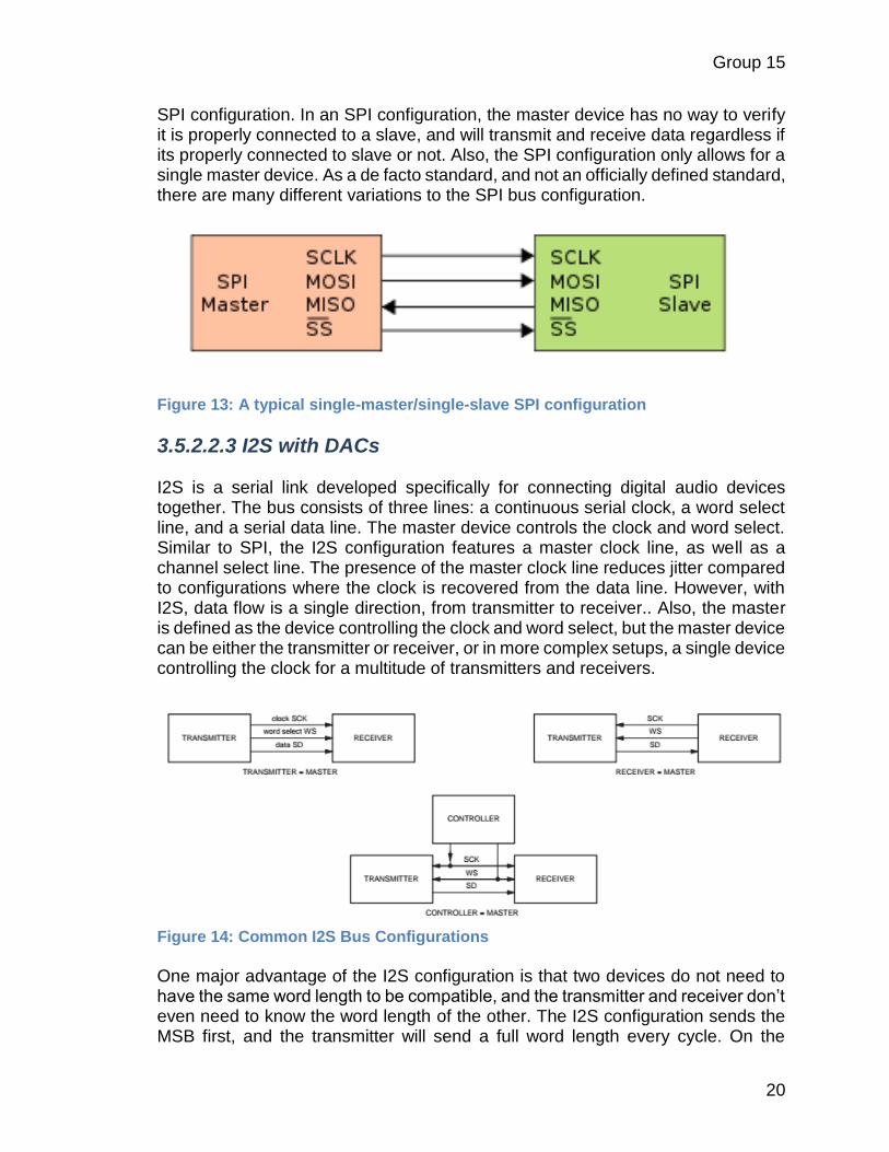
SPI configuration. In an SPI configuration, the master device has no way to verify it is properly connected to a slave, and will transmit and receive data regardless if its properly connected to slave or not. Also, the SPI configuration only allows for a single master device. As a de facto standard, and not an officially defined standard, there are many different variations to the SPI bus configuration.
Figure 13: A typical single-master/single-slave SPI configuration
3.5.2.2.3 I2S with DACs I2S is a serial link developed specifically for connecting digital audio devices together. The bus consists of three lines: a continuous serial clock, a word select line, and a serial data line. The master device controls the clock and word select. Similar to SPI, the I2S configuration features a master clock line, as well as a channel select line. The presence of the master clock line reduces jitter compared to configurations where the clock is recovered from the data line. However, with I2S, data flow is a single direction, from transmitter to receiver.. Also, the master is defined as the device controlling the clock and word select, but the master device can be either the transmitter or receiver, or in more complex setups, a single device controlling the clock for a multitude of transmitters and receivers.
Figure 14: Common I2S Bus Configurations
One major advantage of the I2S configuration is that two devices do not need to have the same word length to be compatible, and the transmitter and receiver don’t even need to know the word length of the other. The I2S configuration sends the MSB first, and the transmitter will send a full word length every cycle. On the
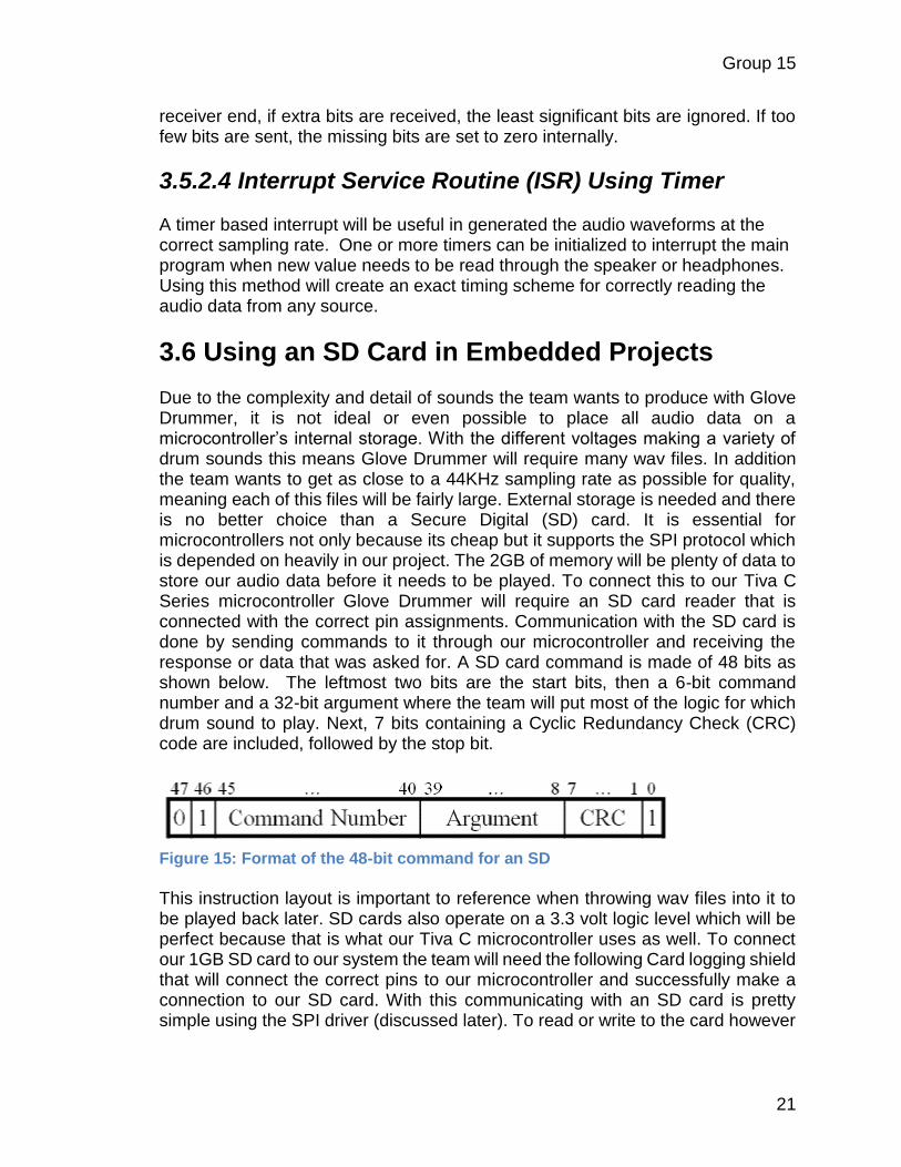
Group 15
21
receiver end, if extra bits are received, the least significant bits are ignored. If too few bits are sent, the missing bits are set to zero internally.
3.5.2.4 Interrupt Service Routine (ISR) Using Timer A timer based interrupt will be useful in generated the audio waveforms at the correct sampling rate. One or more timers can be initialized to interrupt the main program when new value needs to be read through the speaker or headphones. Using this method will create an exact timing scheme for correctly reading the audio data from any source.
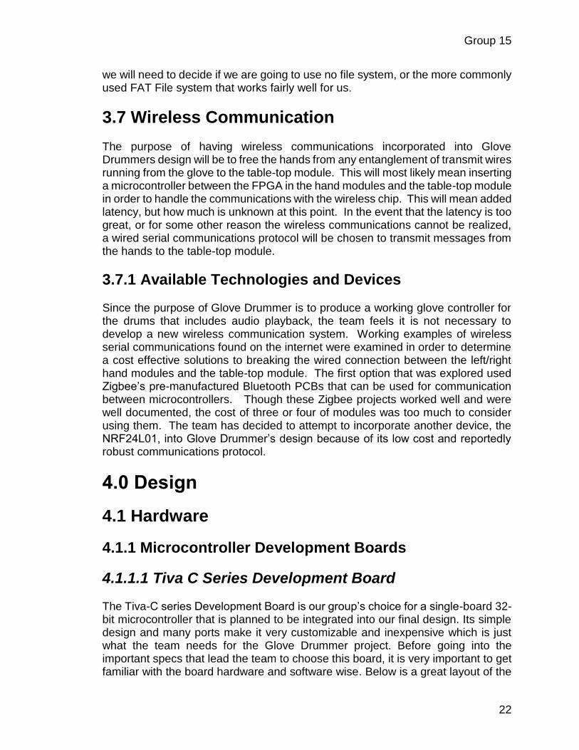
3.6 Using an SD Card in Embedded Projects Due to the complexity and detail of sounds the team wants to produce with Glove Drummer, it is not ideal or even possible to place all audio data on a microcontroller’s internal storage. With the different voltages making a variety of drum sounds this means Glove Drummer will require many wav files. In addition the team wants to get as close to a 44KHz sampling rate as possible for quality, meaning each of this files will be fairly large. External storage is needed and there is no better choice than a Secure Digital (SD) card. It is essential for microcontrollers not only because its cheap but it supports the SPI protocol which is depended on heavily in our project. The 2GB of memory will be plenty of data to store our audio data before it needs to be played. To connect this to our Tiva C Series microcontroller Glove Drummer will require an SD card reader that is connected with the correct pin assignments. Communication with the SD card is done by sending commands to it through our microcontroller and receiving the response or data that was asked for. A SD card command is made of 48 bits as shown below. The leftmost two bits are the start bits, then a 6-bit command number and a 32-bit argument where the team will put most of the logic for which drum sound to play. Next, 7 bits containing a Cyclic Redundancy Check (CRC) code are included, followed by the stop bit.
Figure 15: Format of the 48-bit command for an SD
This instruction layout is important to reference when throwing wav files into it to be played back later. SD cards also operate on a 3.3 volt logic level which will be perfect because that is what our Tiva C microcontroller uses as well. To connect our 1GB SD card to our system the team will need the following Card logging shield that will connect the correct pins to our microcontroller and successfully make a connection to our SD card. With this communicating with an SD card is pretty simple using the SPI driver (discussed later). To read or write to the card however
Group 15
22
we will need to decide if we are going to use no file system, or the more commonly used FAT File system that works fairly well for us.
3.7 Wireless Communication The purpose of having wireless communications incorporated into Glove Drummers design will be to free the hands from any entanglement of transmit wires running from the glove to the table-top module. This will most likely mean inserting a microcontroller between the FPGA in the hand modules and the table-top module in order to handle the communications with the wireless chip. This will mean added latency, but how much is unknown at this point. In the event that the latency is too great, or for some other reason the wireless communications cannot be realized, a wired serial communications protocol will be chosen to transmit messages from the hands to the table-top module.
3.7.1 Available Technologies and Devices Since the purpose of Glove Drummer is to produce a working glove controller for the drums that includes audio playback, the team feels it is not necessary to develop a new wireless communication system. Working examples of wireless serial communications found on the internet were examined in order to determine a cost effective solutions to breaking the wired connection between the left/right hand modules and the table-top module. The first option that was explored used Zigbee’s pre-manufactured Bluetooth PCBs that can be used for communication between microcontrollers. Though these Zigbee projects worked well and were well documented, the cost of three or four of modules was too much to consider using them. The team has decided to attempt to incorporate another device, the NRF24L01, into Glove Drummer’s design because of its low cost and reportedly robust communications protocol.
4.0 Design
4.1 Hardware
4.1.1 Microcontroller Development Boards
4.1.1.1 Tiva C Series Development Board The Tiva-C series Development Board is our group’s choice for a single-board 32-bit microcontroller that is planned to be integrated into our final design. Its simple design and many ports make it very customizable and inexpensive which is just what the team needs for the Glove Drummer project. Before going into the important specs that lead the team to choose this board, it is very important to get familiar with the board hardware and software wise. Below is a great layout of the

Group 15
23
TM4C123G version the team picked and available ports. The team will most likely reference this all through Senior Design II, whenever needed, to implement something else. There are 40 I/O pins which can be configured for a variety of functions that we will need such as digital inputs (for our card module) digital outputs (for our speakers etc) and man others. This was a deciding factor when choosing our microcontroller, but the real reason was the 80MHz clock processor core that comes on it. This is a lot faster than most microcontrollers, and it is needed for our design. We want to reduce the latency as much as possible when reading and input and outputting a wav file, and this quick processor will definitely help with that. A lot of open source code is available for the Tiva C and has a lot of support from Texas Instruments including a USB library, drivers, and a pre-installed bootloader which allows the board to be re-programmed through the USB. Other notable features include:
32 Kbyte of RAM memory for code storage 2 Kbytes of EEPROM for non-volatile data storage 256-Kbytes of flash memory One RGB user LED Two user switches Available I/O brought out to headers on a 0.1-in (2.54-mm) grid On-board ICDI Reset switch Possibility to use booster packs Two sets of connectors: 40 I/O ports, ISP, USI, JTAG Two CAN modules SPI/UART/I2C (Cable and connector provided by end user) Motion control PWM USB Micro-AB connector:
Device mode default configuration
Host/OTG modes supportable
5 V battery connector Switch-selectable power sources:
ICDI USB device
4.1.1.1.1 TM4C123GH6PM MCU (Chip from Tiva C series Dev Board) The Tiva C series Dev Board that is very likely to be on the teams final system was chosen for many reasons such as its open source support and reliability. But one of the main reasons was because of the powerful microcontroller on the board, the TM4C123GH6PM MCU. This microcontroller is one of the best performance-wise and most advanced Texas Instruments has to offer for a price that works with the teams’ budget. Its low-power state and exceptional core of 80MHz operation make it the perfect fit for the Glove Drummer which needs extremely low latency in its
Group 15
24
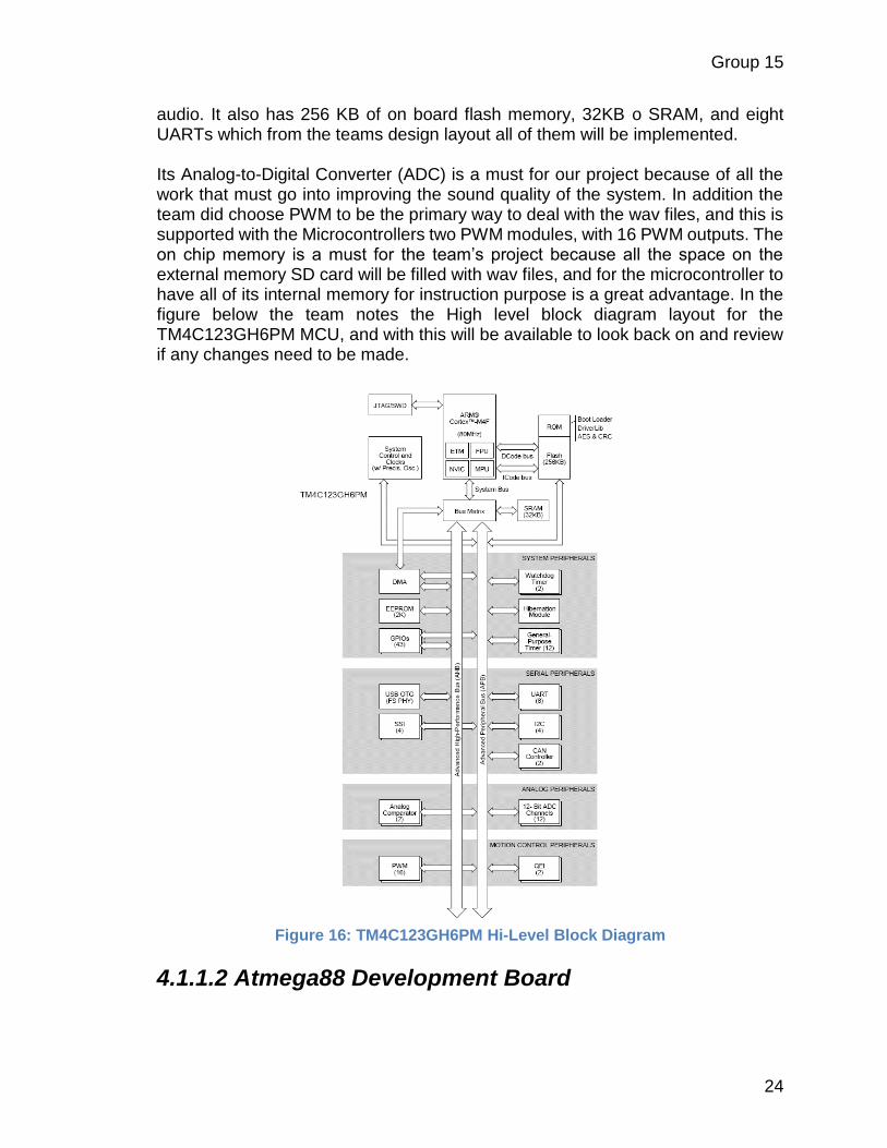
audio. It also has 256 KB of on board flash memory, 32KB o SRAM, and eight UARTs which from the teams design layout all of them will be implemented. Its Analog-to-Digital Converter (ADC) is a must for our project because of all the work that must go into improving the sound quality of the system. In addition the team did choose PWM to be the primary way to deal with the wav files, and this is supported with the Microcontrollers two PWM modules, with 16 PWM outputs. The on chip memory is a must for the team’s project because all the space on the external memory SD card will be filled with wav files, and for the microcontroller to have all of its internal memory for instruction purpose is a great advantage. In the figure below the team notes the High level block diagram layout for the TM4C123GH6PM MCU, and with this will be available to look back on and review if any changes need to be made.
Figure 16: TM4C123GH6PM Hi-Level Block Diagram
4.1.1.2 Atmega88 Development Board

Group 15
25
The Atmega88 development board has an eight bit MCU with a 16MHz clock. Two other important features are the separate USART and SPI ports. These features are important because this device will be meant to use its USART port to receive messages from the FPGA and its SPI to port to then send those messages to the NRF24L01 wireless chip. One well documented open-source code which interfaced two ATmega88s to two NRF24L01 wireless chips through their SPI ports helped the team to select the ATmega88. Since no one on the team has had experience with implementing wireless in embedded systems, it was thought that this may be the most viable option to eliminate any wires between the hand and tabletop modules. If time permits, in order to reduce latency further, the team may eliminate the ATmega88 from at least the table top module layout as there is open source Energia code available for the Tiva C development board. There are no open source codes or examples of using the NRF24L01 with an FPGA, so most likely the ATmega88 will be included in the hand modules.
4.1.1.3 PIC18F46K22 PAXstarter Development Board The PAXstarter development board containing the PIC18F46K22 microcontroller was initially selected to be the heart of the hand modules because of the fact that so many MIDI controller designs incorporate an MCU from the PIC18F family. The electronic drum set found at edrum.info and the Brain series MIDI controllers are two examples using PIC18F MCUs. The PAXstarter has a ten bit ADC which time-division multiplexes up to 30 analog input channels making it more than suitable to work with Glove Drummer’s six analog sensors. It also features a 16MHz clock and Phase Lock Loop (PLL) circuit allowed clock multiplication up to 64MHz. Although the PAXstarter board would have been a good choice for the hand modules there were some factors that made it a less attractive option when compared to an FPGA. The first most obvious reason is that MCUs execute instructions sequentially and can be prone to timing issues (ie. latency) if they are given too many tasks. FPGAs are synthesized from Verilog to create many parallel circuits as can fit within their reconfigurable digital fabric and are much less likely to suffer from any latency issues. Another reason that the PAXstarter board was not chosen as the heart of the hand modules was the multitude of compilers and IDEs available for Microchip products. Over the past ten years or so Microchip MCUs have gone through a series of different supported compilers and IDEs. The team found that open source codes available for the NRF24L01 wireless chip were not written recently and would require porting the newest compiler library.
4.1.2 FPGA Development Board: The Spartan X3CS500E Core Board Having chosen to implement the hand modules with an FPGA, the team chose the Waveshare Spartan 3e development board. This board does not have many features found on other FPGA boards like displays, buttons, switches, various

Group 15
26
ports as they are not required in the hand modules. It features the Xilinx Spartan XC3S500E FPGA chip which has 500K equivalent logic gates and has almost 200 3.3V tolerant I/O pins. The board also includes a 50MHz system clock. It accepts 5V DC power which is regulated to 3.3V, which means that when interfacing to a 5V ADC a bidirectional logic level translator must be used. The team has decided to use level shifters, in comparison to voltage dividers to attenuate the interrupt signal and data outputs of the ADC. This decision was made in order to keep the rise/fall times as fast as possible and to consume less power. Since the team has now decided on the ADC0820 to interface with the FPGA, it has been determined that only shifting from 5V to 3.3V would be necessary as the ADC0820 will accept TTL voltages at its inputs. This basically means that a 3.3V signal will be accepted as a logical ‘one’ by the ADC0820. The team plans to interface the FPGA in the hand modules not only to the ADC0820, but also to the table-top module. If a wireless connection between the hand and tabletop modules is realized, an ATmega88 MCU will most likely interface to the FPGA UART. The ATmega88 in this case will serve to relay sensor information from the FPGA to the NRF24L01 wireless chip. The wireless chip would then relay that information to the wireless chip within the tabletop module. There is also a possibility of eliminating the ATmega88 from this configuration if a SPI port Verilog module can be realized. In the event that the wireless technology cannot be effectively implemented in Glove Drummer’s design, then a wired connection via the UART will be used instead.
4.1.3 UART to PC Interfaces
4.1.3.1 CP2102 5V Logic Level UART/ USB Interface This converter was initially used with the PAXstarter development board in order to verify the functionality of the UART and ADC. It connected the UART transmit pin of the MCU to the USB port of the PC where the data was displayed by Realterm terminal software. A Voltage divider with potentiometer powered from 5V was used to form ratiometric transducers. When the potentiometer wiper was turned all the way in one direction RealTerm displayed 0x00, equivalent to a value of 0V. When the wiper was turned to the extreme in the other direction, RealTerm displayed a value 0x7F. This was equivalent to 5V as the ten bit ADC result was shifted down the seven bits to conform to the MIDI standard.
4.1.3.2 FT232RL 3.3V Logic Level UART/ USB Interface Once the decision was made to use the 3.3V Spartan FPGA instead of the PAXstarter to send sensor information to the tabletop module, the FT232RL 3.3V UART to USB converter board was purchased. Initial tests of the UART verilog module used this board to connect the transmit pin to the USB port of the PC as in section 3.1.3.1 above. Another alternative would have been to use an oscilloscope
Group 15
27
in the senior design lab, however these tests were performed off-campus and would not have been possible without the FT232. It should be noted that the synchronous communication between a SPI or USART port and a PC is not possible with this chip or any other chip if the PC is meant to be the slave device. This means that if the team wishes to view the messages sent from a synchronous master device, the oscilloscope must be used. There is one other option available in this situation and it would be to use the “loop-back method.” This method connects the synchronous serial output to another serial input on the MCU and correct transmission can then be confirmed by the lighting of an LED or by some other means.
4.1.4 Connection Between Left/ Right Hand Modules and Table-top Module
4.1.4.1 A ‘Wired’ UART Connection In order for the tabletop module to create drum sounds based on the sensor information from the hand modules some sort of connection must be made between them. A wireless connection would be preferable in order to allow the hands to move more freely, however it adds a degree of difficulty. If wireless communications cannot be realized during the timespan of Senior Design II, then a wired connection between the FPGA’s UART transmit pin and the Tiva C’s UART receive pin will be used. In this case, the need for a battery in the hand modules would be eliminated and 5V would be sent from the tabletop module to the FPGA. This method would however result in less latency between the strike of a sensor and the creation of sound as there are less devices relaying the sensor information.
4.1.4.2 A Wireless Connection with the NRF24L01 RF Module As stated previously, a wireless connection between the hand and tabletop module would be preferable. However it will mean introducing an unknown amount of latency to the system because of the added devices in the signal chain. Whether or not the exact amount of latency will be an issue remains to be seen. The implementation of wireless communication is less critical than all other design elements and will not be implemented if for instance the team has difficulty with any latency. Design specs like the creation of sound within 15ms of striking the sensor are much more important. In Figure 9 below, one possible hardware configuration that uses the NRF24L01 chip is illustrated.

Group 15
28
Figure 17: Wireless hardware configuration using the Atmega88 to relay messages
4.1.4.2.1 Communicating with the NRF24L01 via Serial Peripheral Interface (SPI) Protocol The Atmega88 will utilize SPI in order to communicate with the NRF24L01 wireless transmitter. In this configuration, the Atmega88 will act as the master device, while the NRF24L01 will act as the slave, driven by the onboard Atmega88 clock. This master/slave configuration will apply to both the transmitter in the hand modules and the receiver in the table-top modules. The nRF24L01 has 8 pins in total, which will be mapped according to the table below. It should be noted that the Atmega88 is powered by 5V, and the nRF24L01 requires 3.3V. However, the nRF24L01 I/O pins can handle 5V, so no voltage regulation is required for the SPI communication. Most of the pins on the Atmega88 are generic I/O pins by default, with alternate functions available. For instance, the generic I/O pin PB5 can also function as SCK when configured correctly. In accordance with the table below, the Atmega88 will be configured such that PB5 is SCK, PB3 is MOSI, PB4 is MISO, and PD2 acts as an interrupt. The pin connections for PB1 and PB2 are both generic outputs, and can be remapped to any pins as required. Pin PD2 can also be remapped to any pin with interrupt capabilities. Table 4: NRF24L01 pin assignments
nRF24L01 Pin Connect to:
GND (Pin 1) Ground
VCC (Pin 2) 3.3V Power supply
CE (Pin 3) Atmega88 PB1 (Output)
CSN (Pin 4) Atmega88 PB2 (Output)

Group 15
29
SCK (Pin 5) Atmega88 PB5 (SCK)
MOSI (Pin 6) Atmega88 PB3 (MOSI)
MISO (Pin 7) Atmega88 PB4 (MISO)
IRQ (Pin 8) Atmega88 PD2 (Interrupt)
4.1.5 SD Card As discussed in section 2.5, the team has chosen an SD card to be the external memory component which will be responsible for reading/writing and playing back audio files for our Glove Drummer project. Before going into how exactly the Tiva C is going to communicate with the SD card in our system lets look at the basic structure of one. Below is a great block diagram that shows the layout of a generic SD card.
Figure 18: Generic SD card layout
This is a good representation of the SD card the team is going to purchase. The 9-pin interface is for the transfer of data between our microcontroller and the card controller on the SD card. The card control is what Glove Drummer will deal with the most, it will read/write data to the memory as well as read it when asking the SD card for a particular sound. It utilizes the memory core interface when doing these read and writes. Internal registers store the state of the card. The big thing here to look at is how requests are handled by the controller. The types of requests handled are control and data. Control request refer to the allowed access to the multiple SD card registers. Data requests is what the code will mainly be using, as it handles the read/write of data to the memory core. Data requests for ‘write’ in or
Group 15
30
project are going to be structured in a particular way that places the wav file in the memory core using the FAT file system so it can be requested for a read whenever one of our piezo sensors are tripped. It’s an important component to our system because it will be what the speaker is reading from to produce all our sounds. We will have a backup idea however, for if we cannot get the sounds clear enough with a high enough quality. If need be we can connect to our computer running a software that will recognize the input we wish to output and play that particular sound. There are plenty of references on working with SD cards with microcontrollers however so the team should be able to apply that to this project.
4.1.5.1 Communicating with the SD card via Serial Peripheral Interface (SPI) Protocol
Serial Peripheral Interface (SPI) communication is a huge help when talking many USB devices available today. SPI is still utilized as a communication means for some applications using displays, memory cards, sensors, etc. SPI runs using a master/slave set-up and signals can be transmitted between the master and the slave simultaneously. This is called full duplex mode and it really helps for making communication simple. When using many slaves, SPI requires no addressing to differentiate between these slaves. There is no standard communication protocol for SPI.
SPI is used to control peripheral devices and has some advantages over other methods. Because of its simplicity and generality, it is being incorporated in various peripheral ICs. The master IC and the slave IC are tied with three signal lines, SCLK (Serial Clock), MISO (Master-In Slave-Out) and MOSI (Master-Out Slave-In). “The contents of both 8-bit shift registers are exchanged with the shift clock driven by master IC. An additional fourth signal, SS (Slave Select), is utilized to synchronize the start of packet or byte boundary and to facilitate working with multiple slave devices simultaneously.” For one-way transfer devices either of data lines may be omitted. The data bits are shifted in MSB first.
When you get your SD card it is not automatically in SPI mode. To put the SD card in SPI mode you have to set the MOSI and CS lines on the card to a value of1 and toggle SD CLK for at least 74 cycles. After these cycles complete the CS line will be set to 0 and a particular command in binary will be sent to the card, this is the reset command. It puts the SD card into the SPI mode if executed when the CS line is low. The SD card will respond to the reset command by sending a basic 8-bit response on the MISO line. The first bit is always a 0, while the other bits specify any errors that may have occurred when processing the message. The program should continuously toggle the SD CLK signal and keep checking for a command to be sent through the MISO line. (Note* “To ensure the proper operation of the SD card, the SD CLK signal should have a frequency in the range of 100 to 400 kHz.”) Your program will continue to do this check for about 16 clock cycles looking for a response, until the reset command must be sent again. Responses and reading of the SD card will be discussed in 3.2.2.3.1.
Group 15
31
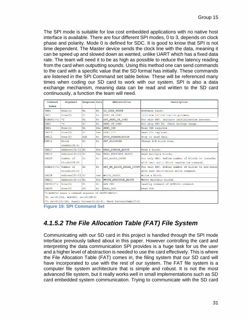
The SPI mode is suitable for low cost embedded applications with no native host interface is available. There are four different SPI modes, 0 to 3, depends on clock phase and polarity. Mode 0 is defined for SDC. It is good to know that SPI is not time dependent. The Master device sends the clock line with the data, meaning it can be speed up and slowed down as wanted, unlike UART which has a fixed data rate. The team will need it to be as high as possible to reduce the latency reading from the card when outputting sounds. Using this method one can send commands to the card with a specific value that the SD format has initially. These commands are listened in the SPI Command set table below. These will be referenced many times when coding our SD card to work with our system. SPI is also a data exchange mechanism, meaning data can be read and written to the SD card continuously, a function the team will need.
Figure 19: SPI Command Set
4.1.5.2 The File Allocation Table (FAT) File System Communicating with our SD card in this project is handled through the SPI mode interface previously talked about in this paper. However controlling the card and interpreting the data communication SPI provides is a huge task for us the user and a higher level of abstraction is needed to use the card effectively. This is where the File Allocation Table (FAT) comes in, the filing system that our SD card will have incorporated to use with the rest of our system. The FAT file system is a computer file system architecture that is simple and robust. It is not the most advanced file system, but it really works well in small implementations such as SD card embedded system communication. Trying to communicate with the SD card

Group 15
32
in our project can be done without the FAT file system, but it makes things much more complicated for us and less organized. The main topic of this section is the index table that FAT uses, called the File Allocation Table. This is produced the moment you format the memory card on any windows machine. Each cell has an entry for each cluster which is an area of disk space where different information of the data is stored. Such things include the number of the next cluster, a flag showing the end of the file, space remaining, and special areas reserved on the disk. With the FAT in place the operating system can look through the table finding the correct cluster number that a particular command is asking for. Through the different FAT file system times, the number of clusters increases to account for the extra disk space. The scaling today for SD cards is FAT12 for 64MB or smaller cards, FAT16 for 128MB to 2GB cards, FAT32 for 4GB to 32GB cards and exFAT for 64GB to 2TB cards. Glove Drummer will use FAT16 because 2GB of space will be plenty for the amount of wav files we plan to write to our SD card. Let us go over the different four sections that are involved in the FAT file system.
Boost Sector: The first sector which contains the boot loader code needed to power up the device. Has the total count of reserved sectors.
FAT Region: Contains two copies of the File Allocation Table for redundancy checking in case something goes wrong. Shows which clusters are used by files and directories.
Root Directory Region: Directory table that stores information on files in the root directory. Creates an allocated fixed size when formatted.
Data Region: The main part of the FAT file system, where the file is stored and takes up most of the available space. The size of files stored here can be added to, as long as they do not go past the reserved space.
As stated before cluster size changes depending on the type of FAT file system being used, in our case FAT16. These clusters ultimately create a chain and are stored on the Data Region. The FAT16 file system uses 16 bits per FAT entry, one entry spans two bytes.
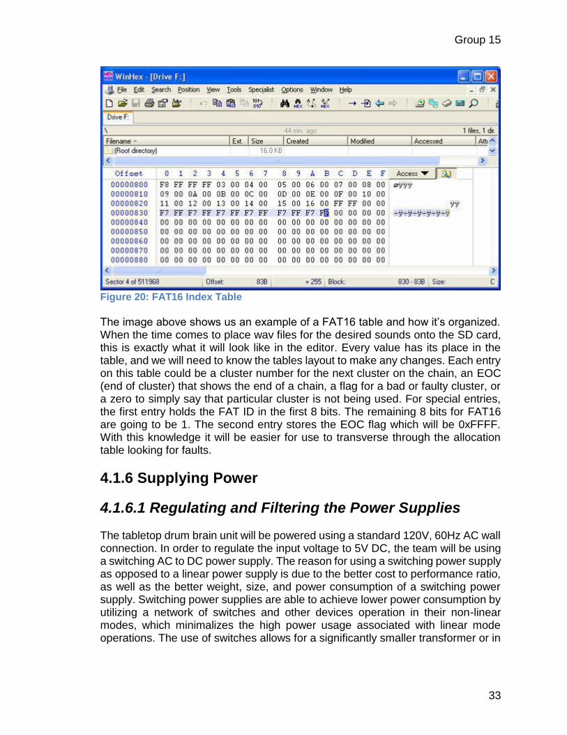
Group 15
33
Figure 20: FAT16 Index Table
The image above shows us an example of a FAT16 table and how it’s organized. When the time comes to place wav files for the desired sounds onto the SD card, this is exactly what it will look like in the editor. Every value has its place in the table, and we will need to know the tables layout to make any changes. Each entry on this table could be a cluster number for the next cluster on the chain, an EOC (end of cluster) that shows the end of a chain, a flag for a bad or faulty cluster, or a zero to simply say that particular cluster is not being used. For special entries, the first entry holds the FAT ID in the first 8 bits. The remaining 8 bits for FAT16 are going to be 1. The second entry stores the EOC flag which will be 0xFFFF. With this knowledge it will be easier for use to transverse through the allocation table looking for faults.
4.1.6 Supplying Power
4.1.6.1 Regulating and Filtering the Power Supplies The tabletop drum brain unit will be powered using a standard 120V, 60Hz AC wall connection. In order to regulate the input voltage to 5V DC, the team will be using a switching AC to DC power supply. The reason for using a switching power supply as opposed to a linear power supply is due to the better cost to performance ratio, as well as the better weight, size, and power consumption of a switching power supply. Switching power supplies are able to achieve lower power consumption by utilizing a network of switches and other devices operation in their non-linear modes, which minimalizes the high power usage associated with linear mode operations. The use of switches allows for a significantly smaller transformer or in
Group 15
34
some cases no transformer at all, which accounts for the decreased weight and size of switching power supplies. Also, the power supply used for the table top unit will be regulated. A regulated power supply is required because many of the chips inside the drum brain will require a strict 3.3V or 5V input. If using an unregulated power supply, design the supply to output the required voltage with high precision would require knowing the total load that will be connected. A regulated power supply, however, can be designed to output the correct voltage, and it will vary only very slightly for any connected load. In order regulate the power supply, a simple voltage regulator IC will be placed at the output of the power supply. It should be noted that in order to regulate to a 5V output, the IC must receive approximately 8V. When using any AC to DC power supply, the input must pass through a rectifier circuit. When a rectifier converts AC to DC, it doesn’t do so perfectly. The DC output will have high frequency ripples that can cause spikes in output voltage. In order to remove these, a filter circuit is applied at the output. This output filter can consist of reservoir capacitors and low pass filters. Used in combination, these elements can create very near true DC output.
4.1.6.2 Powering the Left/ Right Hand Modules Unlike the table top drum brain module, the hand modules will require freedom of motion in order to properly function. As such, connecting them to a wall outlet as with the tabletop module is impractical. Instead, the hand modules will receive power from a battery source. When considering potential battery sources, several needs come to mind for the hand modules. First, the batteries need to reliably provide enough power long enough for the user to play an extended set of music. Second, the battery source must be lightweight and small enough so that it does not restrict the motion of the user. Also, the battery source should be rechargeable, in order to compete with other modern electronics. Given these parameters, Lithium Ion batteries are the most effective battery source. Unlike the tabletop module, the hand modules will be directly supplied with DC voltage by the battery source. Because of this, the hand modules will only require a DC voltage regulator to achieve the correct input voltage.
4.1.6.2.1 18650 Lithium Ion Batteries 18650 Lithium Ion Batteries resemble large AA batteries but have a power density much greater than nickel cadmium and other more traditional battery chemistries. These are the batteries found in cell phones and other personal electronics today. The physical dimensions of the 18650 battery are less desirable than other slim packaged lithium ion batteries because at least one will need to fit inside the hand module project enclosure. Although a slim package may be more ideal, the 18650 was chosen because of its low cost. These batteries also come with IC protection.
Group 15
35
The protection offered by the onboard ICs includes thermal, over voltage, and under voltage. In other words the battery will not charge or discharge so long as the temperature or voltage are out of the acceptable range. Any one of these situations will at least damage the battery, causing failure. At worst, the battery may catch fire. Many power management ICs exist that do all of this and also regulate voltage or serve as a charging system. Glove Drummer will use an IC protected 18650 battery along with power management ICs. At this point the team plans to use only one single cell lithium ion battery with a 3000mAh capacity opposed to any parallel or series combination of batteries. Using only one cell will make selecting power management ICs much easier but may supply inadequate power to play for long periods of time. The power management ICs used will take care of charging the battery, regulating its output, and the selecting a “power path.” Dynamic power path control is term that T.I. uses to describe the switching of what the power supply to the load when a power source other than the battery (a wall wart) is connected to the system. In this case, the wall wart supplies current both for system operation and for charging of the battery. Not much has been documented on using an IC for power path management, the team hopes to use the BQ24072 for this purpose. Another alternative of course would be to remove the battery from the hand modules for charging, but this would be much less convenient given that screws will need to be removed to do this. Another issue in power management is voltage regulation. Switching regulators are preferred here for power consumption reasons. Another disadvantage to using a single cell is that to produce a 5V supply rail, a “boost” regulator will be required. If two cells were placed in series, then a more efficient “buck” regulator could be used. One very important property of these batteries is that their 3.7 or 3.6V rating is a nominal rating. When they are fully charged they hold ~4.2V, and once fully discharged they hold ~3V. That means in order to provide a 3.6V supply rail, a buck/ boost regulator is needed. What this regulator does is buck its output to 3.3V when its input is above 3.3V and boost its output to 3.3V when its input falls below 3.3V.
4.1.6.2.3 Extending Battery Life Sacrificing performance to save battery life is a compromise the team does not want to have to make. Nonetheless some sacrifices must be made in order for the batteries to last long enough for the user to enjoy playing with Glove Drummer. Some techniques that might be used to save battery power are using ICs designed for low power consumption, reducing clock speed, reducing sampling frequency, and using PWM to drive LEDs when possible. Because of the fact that the human eye cannot perceive an LED turning off and on very quickly, the team can exploit this phenomena in order to reduce power

Group 15
36
consumption. Persistence of vision is defined as seeing an image 1/25 of a second after the image has disappeared (source4). This means that if a status LED used in the Glove Drummer’s design is driven with pulse width modulation so that its “off“ period is less than 1/25 of a second then there will be no perceived flickering of light. This will save lower power consumption and therefore extend battery life.
4.1.6.3 Powering the Table-top Module No AC to DC conversion will occur within the tabletop module because of the abundance of AC to DC converters today. The team feels that many users may already own a suitable power supply at home that will work with the use of linear DC to DC voltage regulators within the tabletop module. A wall wart supply with a minimum current capability of 500mA operating at a voltage between 7V and 15V should be suitable.
4.1.7 Hardware for Expanded Mapping Flexibility and Hi Hat Control
4.1.7.1 Infrared (IR) Proximity Sensors Infrared proximity sensors are ratiometric transducers which bounce infrared light off of an object and read the reflected light to sense if an object is in close proximity. The most basic IR sensor would contain one IR LED which is powered from a voltage source with a current limiting resistor in series. Current limiting is needed to avoid burning out the IR LED. Next to the first IR LED would be another IR LED that is not powered but instead receives reflected light from the first IR LED. A divider must be placed in between the two LEDs so that only reflected IR light is creates a voltage difference across the terminals of the second LED. If a MCU were to read a voltage difference from the second LED, it would know there is some solid object some distance from this crude proximity sensor. This design would be prone to producing errors stemming from ambient light conditions. One possible improvement on this design is to cover the second LED in an “IR pass filter.” This type of filter is actually a film applied over the second LED which only allows IR light to pass through. In order to improve the accuracy of the proximity sensor further, PWM may be used to drive the first LED. Doing so allows for the LED to burn brighter in short bursts without exceeding the maximum average current rating of the diode, resulting the ability to sense objects from a farther distance. An adding benefit to this design modification can be realized by adding a band pass filter circuit to the second LED circuit. The frequency of the PWM driving the first LED would be in the pass band of this BP circuit so that only reflected IR light driven at this specific frequency would be sensed. IR proximity sensors using this technique will be far less prone to errors from ambient visible or IR light. This is an example of amplitude modulation where the IR light serves as the carrier wave.
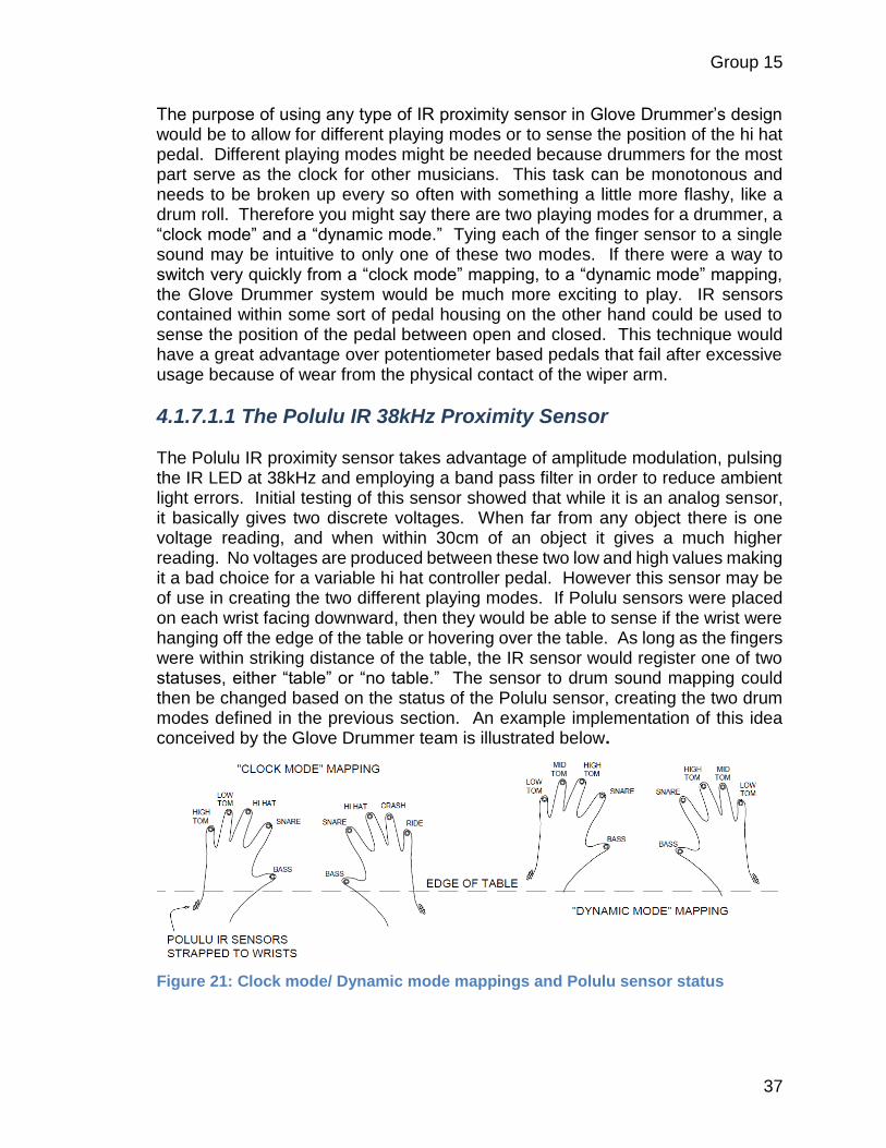
Group 15
37
The purpose of using any type of IR proximity sensor in Glove Drummer’s design would be to allow for different playing modes or to sense the position of the hi hat pedal. Different playing modes might be needed because drummers for the most part serve as the clock for other musicians. This task can be monotonous and needs to be broken up every so often with something a little more flashy, like a drum roll. Therefore you might say there are two playing modes for a drummer, a “clock mode” and a “dynamic mode.” Tying each of the finger sensor to a single sound may be intuitive to only one of these two modes. If there were a way to switch very quickly from a “clock mode” mapping, to a “dynamic mode” mapping, the Glove Drummer system would be much more exciting to play. IR sensors contained within some sort of pedal housing on the other hand could be used to sense the position of the pedal between open and closed. This technique would have a great advantage over potentiometer based pedals that fail after excessive usage because of wear from the physical contact of the wiper arm.
4.1.7.1.1 The Polulu IR 38kHz Proximity Sensor The Polulu IR proximity sensor takes advantage of amplitude modulation, pulsing the IR LED at 38kHz and employing a band pass filter in order to reduce ambient light errors. Initial testing of this sensor showed that while it is an analog sensor, it basically gives two discrete voltages. When far from any object there is one voltage reading, and when within 30cm of an object it gives a much higher reading. No voltages are produced between these two low and high values making it a bad choice for a variable hi hat controller pedal. However this sensor may be of use in creating the two different playing modes. If Polulu sensors were placed on each wrist facing downward, then they would be able to sense if the wrist were hanging off the edge of the table or hovering over the table. As long as the fingers were within striking distance of the table, the IR sensor would register one of two statuses, either “table” or “no table.” The sensor to drum sound mapping could then be changed based on the status of the Polulu sensor, creating the two drum modes defined in the previous section. An example implementation of this idea conceived by the Glove Drummer team is illustrated below.
Figure 21: Clock mode/ Dynamic mode mappings and Polulu sensor status
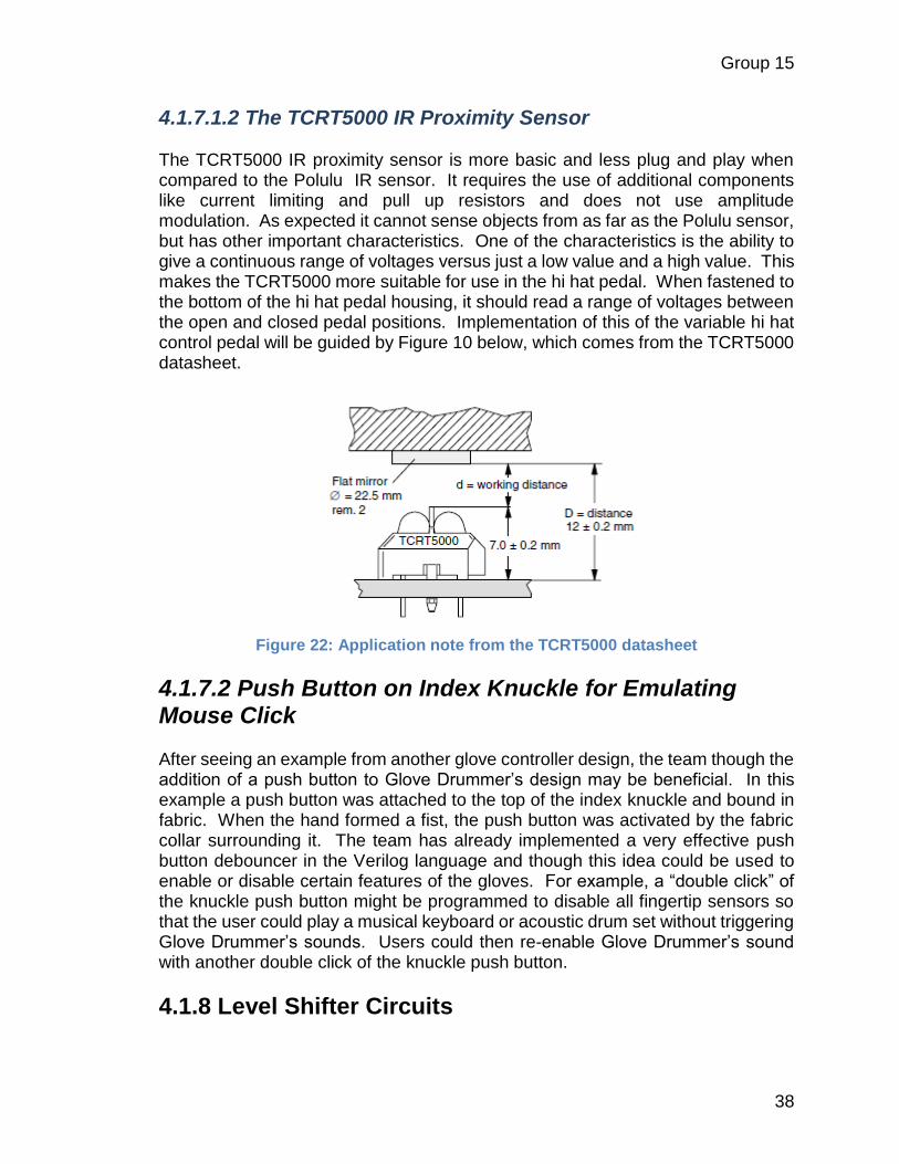
Group 15
38
4.1.7.1.2 The TCRT5000 IR Proximity Sensor The TCRT5000 IR proximity sensor is more basic and less plug and play when compared to the Polulu IR sensor. It requires the use of additional components like current limiting and pull up resistors and does not use amplitude modulation. As expected it cannot sense objects from as far as the Polulu sensor, but has other important characteristics. One of the characteristics is the ability to give a continuous range of voltages versus just a low value and a high value. This makes the TCRT5000 more suitable for use in the hi hat pedal. When fastened to the bottom of the hi hat pedal housing, it should read a range of voltages between the open and closed pedal positions. Implementation of this of the variable hi hat control pedal will be guided by Figure 10 below, which comes from the TCRT5000 datasheet.
Figure 22: Application note from the TCRT5000 datasheet
4.1.7.2 Push Button on Index Knuckle for Emulating Mouse Click After seeing an example from another glove controller design, the team though the addition of a push button to Glove Drummer’s design may be beneficial. In this example a push button was attached to the top of the index knuckle and bound in fabric. When the hand formed a fist, the push button was activated by the fabric collar surrounding it. The team has already implemented a very effective push button debouncer in the Verilog language and though this idea could be used to enable or disable certain features of the gloves. For example, a “double click” of the knuckle push button might be programmed to disable all fingertip sensors so that the user could play a musical keyboard or acoustic drum set without triggering Glove Drummer’s sounds. Users could then re-enable Glove Drummer’s sound with another double click of the knuckle push button.
4.1.8 Level Shifter Circuits
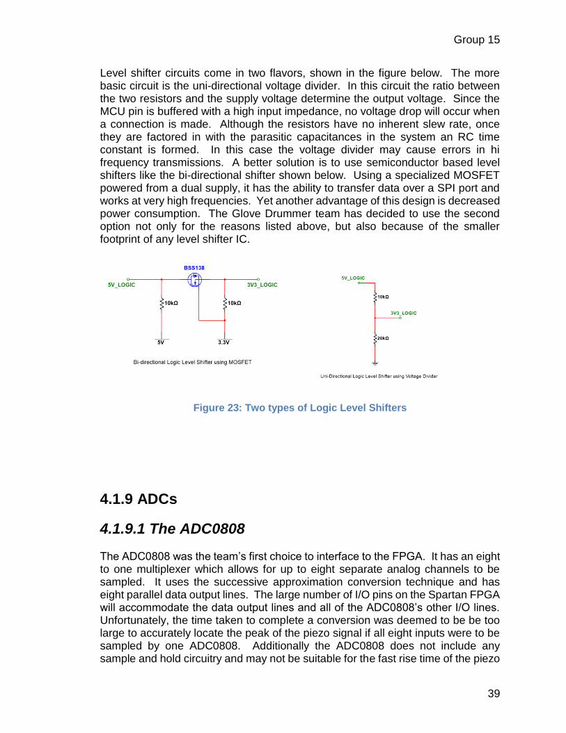
Group 15
39
Level shifter circuits come in two flavors, shown in the figure below. The more basic circuit is the uni-directional voltage divider. In this circuit the ratio between the two resistors and the supply voltage determine the output voltage. Since the MCU pin is buffered with a high input impedance, no voltage drop will occur when a connection is made. Although the resistors have no inherent slew rate, once they are factored in with the parasitic capacitances in the system an RC time constant is formed. In this case the voltage divider may cause errors in hi frequency transmissions. A better solution is to use semiconductor based level shifters like the bi-directional shifter shown below. Using a specialized MOSFET powered from a dual supply, it has the ability to transfer data over a SPI port and works at very high frequencies. Yet another advantage of this design is decreased power consumption. The Glove Drummer team has decided to use the second option not only for the reasons listed above, but also because of the smaller footprint of any level shifter IC.
Figure 23: Two types of Logic Level Shifters
4.1.9 ADCs
4.1.9.1 The ADC0808 The ADC0808 was the team’s first choice to interface to the FPGA. It has an eight to one multiplexer which allows for up to eight separate analog channels to be sampled. It uses the successive approximation conversion technique and has eight parallel data output lines. The large number of I/O pins on the Spartan FPGA will accommodate the data output lines and all of the ADC0808’s other I/O lines. Unfortunately, the time taken to complete a conversion was deemed to be be too large to accurately locate the peak of the piezo signal if all eight inputs were to be sampled by one ADC0808. Additionally the ADC0808 does not include any sample and hold circuitry and may not be suitable for the fast rise time of the piezo

Group 15
40
signal. The ADC0808 is more suited to sampling slow signals such as indoor air temperature unless external sample and hold circuits can be added. After discovering these problems, the team has decided to find another ADC to sample the piezo signals.
4.1.9.2 The ADC0820 The ADC0820 is an eight bit, half-flash ADC with sample and hold circuitry. It lacks the onboard multiplexer of the ADC0808, but has a much faster conversion time. The datasheet specifies conversion times of 2us to less than 1us depending on the mode of operation. Operation modes include Read and Write modes with the latter being able to complete a conversion in 700ns. The team has decided to use a sampling frequency much higher than the Nyquist frequency in this situation as the Nyquist Shannon Sampling theory applies only to continuous signals. Multiple possible configurations will be explored two or more ADC0820 ICs in parallel, each one using a DG508 eight to one multiplexer. The number of lines multiplexed by the DG508 will be determined by the maximum sampling frequency allowed using that number of inputs. If a peak cannot be accurately found using all eight of the DG508’s inputs, then the number of inputs will be decreased until a high enough sampling frequency is achieved. One downside to using this ADC with the Spartan FPGA is the incompatibility of the their respective voltage levels. While the ADC0820 will accept 3.3V as logical ‘1’, its nine total output lines will have to be shifted from 5V to 3.3V with external circuitry. Also, the effect of not shifting the 3.3V control lines from the FPGA to 5V remains to be seen. Though it is possible, it may be far from optimal. In either case, many lines will exist between a number of ADC0820s and the Spartan FPGA that require logic level shifting. The team plans to find an IC for this purpose which may include up to 32 bits of logic level conversion. Texas Instruments for example makes an IC just like this. Hopefully using such a device will decrease the footprint of analog circuitry on the Glove Drummer PCB. The connections made between the sensors and the ADC must also conform to a certain standard. Since the ADC will be biased between ground and +5V, its analog inputs must be contained within that voltage range. Also the sensors’ output impedance must be kept below a certain value in order to make accurate conversions. This is the reason for the analog signal conditioning circuitry discussed in Section 5.0. The resulting signal that is sourced from the analog conditioning circuitry has a very low output impedance and is bound in magnitude between ground and +5V. In order to explore the operation of the ADC0820, the team has decided to begin experimenting with the chip in “Read” mode. A timing diagram for read mode is shown in the figure below. This is the more basic of the two modes where a conversion is started by driving the (read)’ line low. The FPGA will know a conversion is complete when the (int)’ line is driven low by the ADC. Shortly after
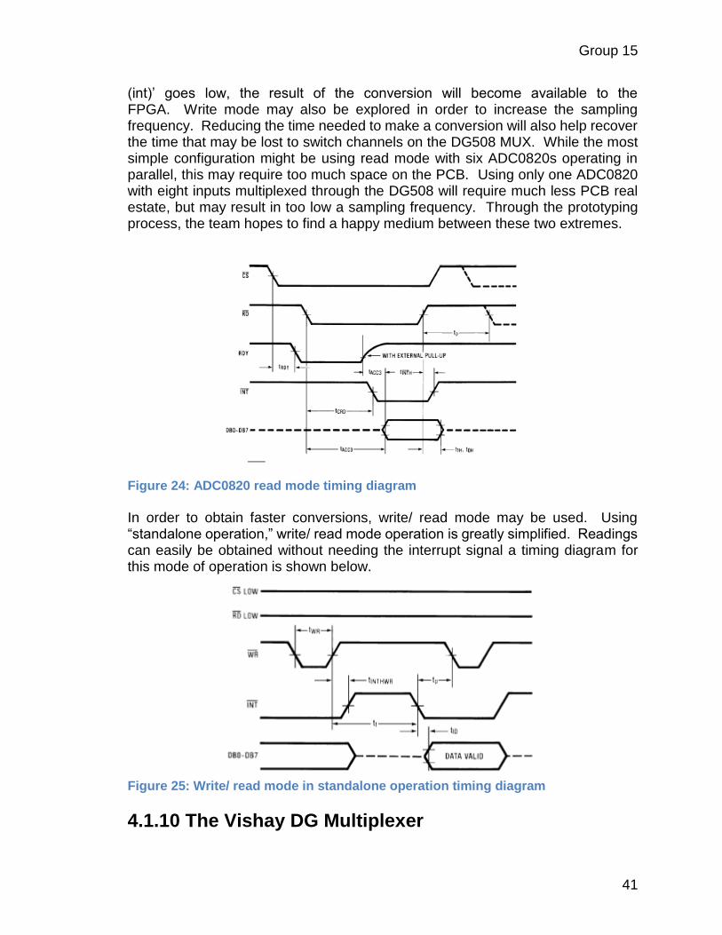
Group 15
41
(int)’ goes low, the result of the conversion will become available to the FPGA. Write mode may also be explored in order to increase the sampling frequency. Reducing the time needed to make a conversion will also help recover the time that may be lost to switch channels on the DG508 MUX. While the most simple configuration might be using read mode with six ADC0820s operating in parallel, this may require too much space on the PCB. Using only one ADC0820 with eight inputs multiplexed through the DG508 will require much less PCB real estate, but may result in too low a sampling frequency. Through the prototyping process, the team hopes to find a happy medium between these two extremes.
Figure 24: ADC0820 read mode timing diagram
In order to obtain faster conversions, write/ read mode may be used. Using “standalone operation,” write/ read mode operation is greatly simplified. Readings can easily be obtained without needing the interrupt signal a timing diagram for this mode of operation is shown below.
Figure 25: Write/ read mode in standalone operation timing diagram
4.1.10 The Vishay DG Multiplexer
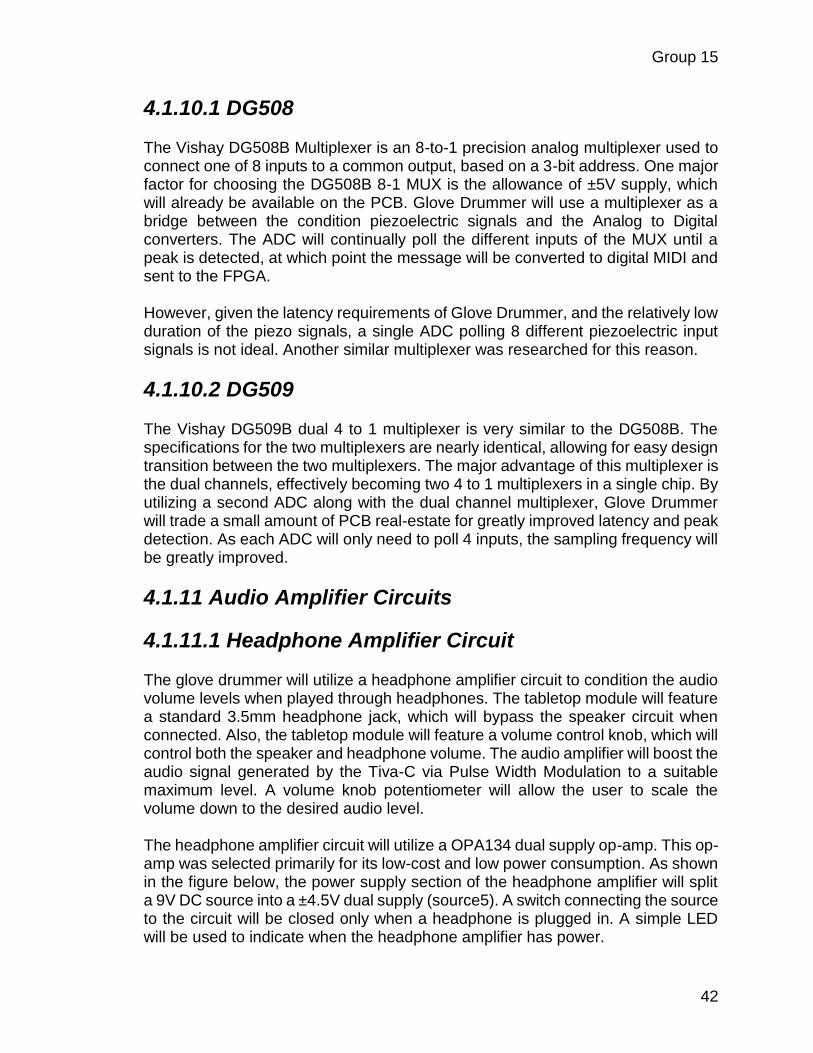
Group 15
42
4.1.10.1 DG508 The Vishay DG508B Multiplexer is an 8-to-1 precision analog multiplexer used to connect one of 8 inputs to a common output, based on a 3-bit address. One major factor for choosing the DG508B 8-1 MUX is the allowance of ±5V supply, which will already be available on the PCB. Glove Drummer will use a multiplexer as a bridge between the condition piezoelectric signals and the Analog to Digital converters. The ADC will continually poll the different inputs of the MUX until a peak is detected, at which point the message will be converted to digital MIDI and sent to the FPGA. However, given the latency requirements of Glove Drummer, and the relatively low duration of the piezo signals, a single ADC polling 8 different piezoelectric input signals is not ideal. Another similar multiplexer was researched for this reason.
4.1.10.2 DG509 The Vishay DG509B dual 4 to 1 multiplexer is very similar to the DG508B. The specifications for the two multiplexers are nearly identical, allowing for easy design transition between the two multiplexers. The major advantage of this multiplexer is the dual channels, effectively becoming two 4 to 1 multiplexers in a single chip. By utilizing a second ADC along with the dual channel multiplexer, Glove Drummer will trade a small amount of PCB real-estate for greatly improved latency and peak detection. As each ADC will only need to poll 4 inputs, the sampling frequency will be greatly improved.
4.1.11 Audio Amplifier Circuits
4.1.11.1 Headphone Amplifier Circuit The glove drummer will utilize a headphone amplifier circuit to condition the audio volume levels when played through headphones. The tabletop module will feature a standard 3.5mm headphone jack, which will bypass the speaker circuit when connected. Also, the tabletop module will feature a volume control knob, which will control both the speaker and headphone volume. The audio amplifier will boost the audio signal generated by the Tiva-C via Pulse Width Modulation to a suitable maximum level. A volume knob potentiometer will allow the user to scale the volume down to the desired audio level. The headphone amplifier circuit will utilize a OPA134 dual supply op-amp. This op-amp was selected primarily for its low-cost and low power consumption. As shown in the figure below, the power supply section of the headphone amplifier will split a 9V DC source into a ±4.5V dual supply (source5). A switch connecting the source to the circuit will be closed only when a headphone is plugged in. A simple LED will be used to indicate when the headphone amplifier has power.
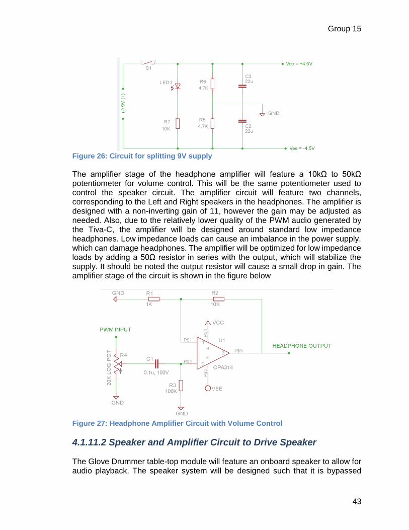
Group 15
43
Figure 26: Circuit for splitting 9V supply
The amplifier stage of the headphone amplifier will feature a 10kΩ to 50kΩ potentiometer for volume control. This will be the same potentiometer used to control the speaker circuit. The amplifier circuit will feature two channels, corresponding to the Left and Right speakers in the headphones. The amplifier is designed with a non-inverting gain of 11, however the gain may be adjusted as needed. Also, due to the relatively lower quality of the PWM audio generated by the Tiva-C, the amplifier will be designed around standard low impedance headphones. Low impedance loads can cause an imbalance in the power supply, which can damage headphones. The amplifier will be optimized for low impedance loads by adding a 50Ω resistor in series with the output, which will stabilize the supply. It should be noted the output resistor will cause a small drop in gain. The amplifier stage of the circuit is shown in the figure below
Figure 27: Headphone Amplifier Circuit with Volume Control
4.1.11.2 Speaker and Amplifier Circuit to Drive Speaker The Glove Drummer table-top module will feature an onboard speaker to allow for audio playback. The speaker system will be designed such that it is bypassed

Group 15
44
completely when the user plugs a pair of headphones into the table-top module. This will be achieved by utilizing a headphone bypass jack as the headphone connection. A single volume knob will be used to control the volume for both the speaker amplifier and the headphone amplifier. The speaker used will be a standard 5W, 8Ω speaker. The speaker amplifier, shown below in the figure below, will utilize a basic LM386 for audio amplification. The amplifier will be powered by a 9Vdc source, and will initially be designed, as shown, with a maximum gain of 200. Once implemented, the gain can easily be scaled down to the optimum gain by adding a resistor between LM386 pins 1 and 8, in series with the 10µF capacitor shown. The PWM audio is applied at the input, and the 20k potentiometer allows for volume control, from 0 gain up to the maximum designed gain. The circuit schematic is shown in the figure below.
Figure 28: 5W, 8Ω Speaker Amplifier
4.2 Software
4.2.1 C Code Programs
4.2.1.1 C Code for the PIC18F Although the PIC18F will not be used in the final Glove Drummer design, the team learned about using timer interrupts with this MCU. The C code for using a timer interrupt is show in the figure below. In this code, once the timer’s initial value is set, a forever while loop is fallen into. The interrupt service routine (ISR) function written at the bottom of the figure below interrupts the forever while loop whenever the timer overflows. Overflowing is when all bits of the timer are one. When this happens, the interrupt flag is set. It was important to clear the interrupt flag each time after toggling the LED. Another important task was to disable and enable interrupts at the appropriate times. In a system using more than one interrupt
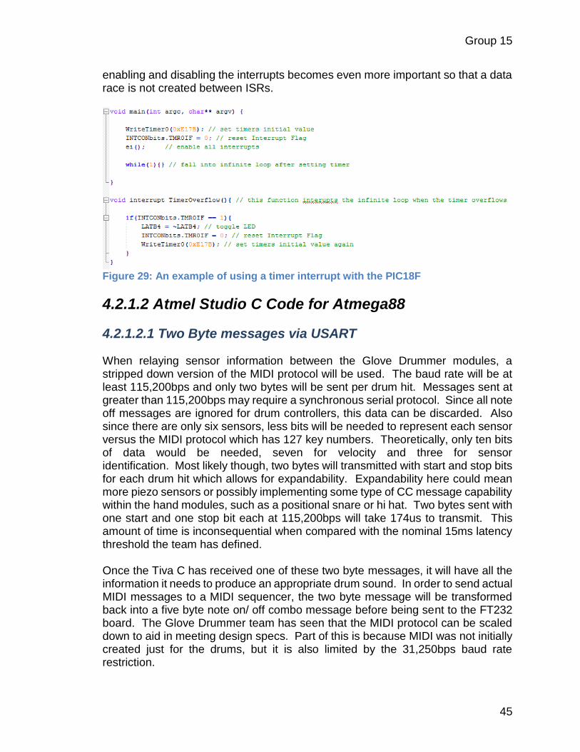
Group 15
45
enabling and disabling the interrupts becomes even more important so that a data race is not created between ISRs.
Figure 29: An example of using a timer interrupt with the PIC18F
4.2.1.2 Atmel Studio C Code for Atmega88
4.2.1.2.1 Two Byte messages via USART When relaying sensor information between the Glove Drummer modules, a stripped down version of the MIDI protocol will be used. The baud rate will be at least 115,200bps and only two bytes will be sent per drum hit. Messages sent at greater than 115,200bps may require a synchronous serial protocol. Since all note off messages are ignored for drum controllers, this data can be discarded. Also since there are only six sensors, less bits will be needed to represent each sensor versus the MIDI protocol which has 127 key numbers. Theoretically, only ten bits of data would be needed, seven for velocity and three for sensor identification. Most likely though, two bytes will transmitted with start and stop bits for each drum hit which allows for expandability. Expandability here could mean more piezo sensors or possibly implementing some type of CC message capability within the hand modules, such as a positional snare or hi hat. Two bytes sent with one start and one stop bit each at 115,200bps will take 174us to transmit. This amount of time is inconsequential when compared with the nominal 15ms latency threshold the team has defined. Once the Tiva C has received one of these two byte messages, it will have all the information it needs to produce an appropriate drum sound. In order to send actual MIDI messages to a MIDI sequencer, the two byte message will be transformed back into a five byte note on/ off combo message before being sent to the FT232 board. The Glove Drummer team has seen that the MIDI protocol can be scaled down to aid in meeting design specs. Part of this is because MIDI was not initially created just for the drums, but it is also limited by the 31,250bps baud rate restriction.
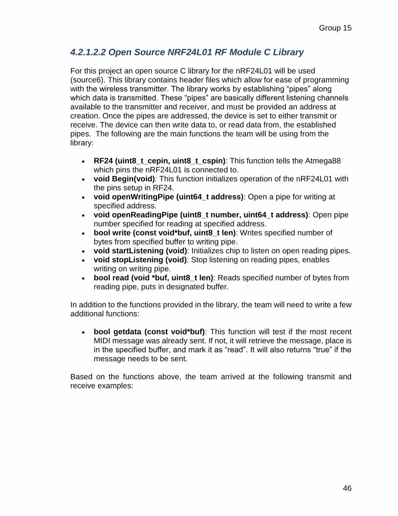
Group 15
46
4.2.1.2.2 Open Source NRF24L01 RF Module C Library For this project an open source C library for the nRF24L01 will be used (source6). This library contains header files which allow for ease of programming with the wireless transmitter. The library works by establishing “pipes” along which data is transmitted. These “pipes” are basically different listening channels available to the transmitter and receiver, and must be provided an address at creation. Once the pipes are addressed, the device is set to either transmit or receive. The device can then write data to, or read data from, the established pipes. The following are the main functions the team will be using from the library:
RF24 (uint8_t_cepin, uint8_t_cspin): This function tells the Atmega88 which pins the nRF24L01 is connected to.
void Begin(void): This function initializes operation of the nRF24L01 with the pins setup in RF24.
void openWritingPipe (uint64_t address): Open a pipe for writing at specified address.
void openReadingPipe (uint8_t number, uint64_t address): Open pipe number specified for reading at specified address.
bool write (const void*buf, uint8_t len): Writes specified number of bytes from specified buffer to writing pipe.
void startListening (void): Initializes chip to listen on open reading pipes. void stopListening (void): Stop listening on reading pipes, enables
writing on writing pipe. bool read (void *buf, uint8_t len): Reads specified number of bytes from
reading pipe, puts in designated buffer.
In addition to the functions provided in the library, the team will need to write a few additional functions:
bool getdata (const void*buf): This function will test if the most recent MIDI message was already sent. If not, it will retrieve the message, place is in the specified buffer, and mark it as “read”. It will also returns “true” if the message needs to be sent.
Based on the functions above, the team arrived at the following transmit and receive examples:
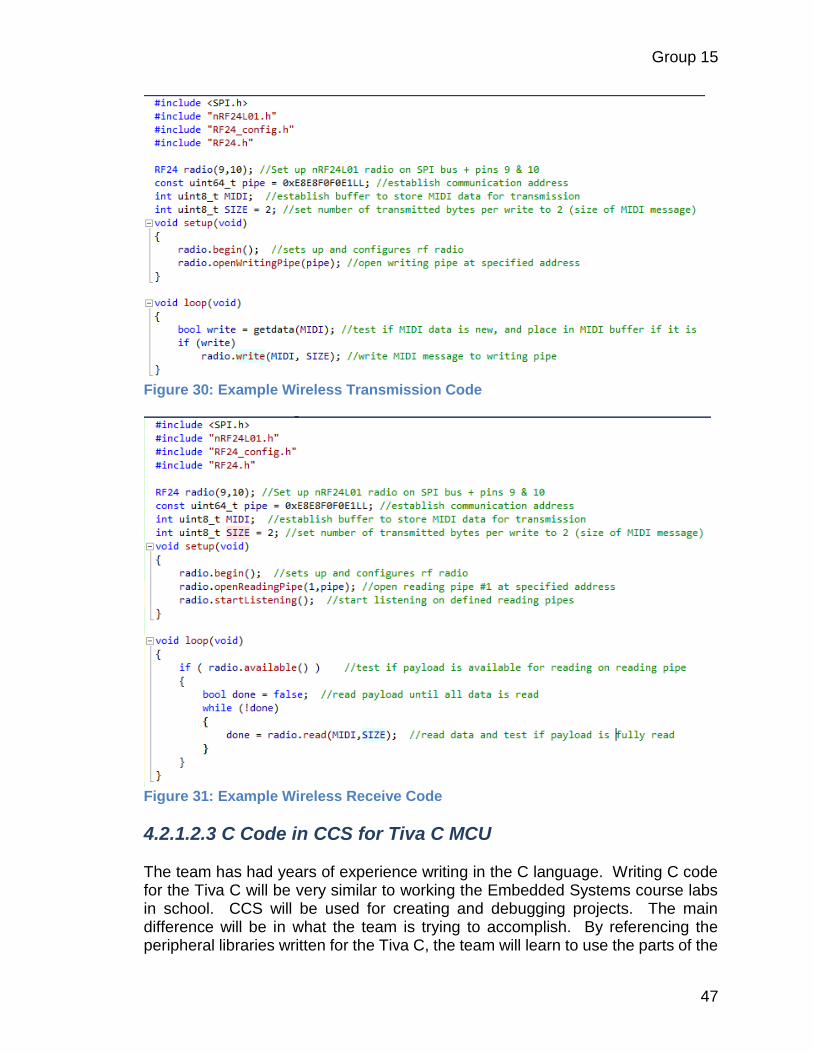
Group 15
47
Figure 30: Example Wireless Transmission Code
Figure 31: Example Wireless Receive Code
4.2.1.2.3 C Code in CCS for Tiva C MCU The team has had years of experience writing in the C language. Writing C code for the Tiva C will be very similar to working the Embedded Systems course labs in school. CCS will be used for creating and debugging projects. The main difference will be in what the team is trying to accomplish. By referencing the peripheral libraries written for the Tiva C, the team will learn to use the parts of the
Group 15
48
chip that relate to the Glove Drummer project. Another added advantage of using CCS is the ability to export projects from Energia to CCS. Energia provides additional abstractions and many well written libraries and by porting to C, the codes performance can be further improved.
4.2.2 Energia Code for Tiva C series In short Energia is an open source software framework that gives us an easier way to communicate and manipulate our Tiva C Series microcontroller. A lot of the code is reusable and the team has already taken down a few code segments that will help with the multiple SPI communications that are needed. The API’s are not so hard to pick up so this will help with the teams pressured time constraint to pick up new ways of coding. Many libraries help developers make the code optimal to everyday use. And of course since Energia has been used with Texas Instruments launch pads there is a huge community of support and for it. There are many ways to advance on the code we are making, so the Glove Drummer team can focus on other tasks.
4.2.2.1 On-Board ADC It is nearly decided that for our project the team will be using the Tiva C microcontroller for handling a few of our processes. Because of this the team will be using the On-Board ADC to handle all digital audio the team will record onto the SD card and all that will playback. This analog voltage converted into a discrete digital number is an important process of our project. Two converter modules are on the board, one of which if fully dedicated to be our ADC with 12 input channels. It is the TM4C123GH6PM, and the team picked it for a few reasons. Just one module has four programmable sequencers which let us work with multiple analog inputs at one time without interruption. The team needed our ADC to have an easily configurable input source, dependable trigger events, sequencer priority and interrupt generation. It can also be switched to digital to analog converter for our playback. Having eight digital comparators means cleaner conversions. The team also notes that there are two onboard ADCs, and if the other does not have many instructions to handle it can do some of the conversion for us and this may reduce any latency the team might come across. Other notable abilities of our ADC is that it has an on-chip internal temperature sensor, very good sample rate which the team will need (one million samples/second),and flexible trigger control. Another notable thing the team came across when researching this ADC is its prioritization. When sampling events trigger at the same time, they go into the ADC Sample Sequencer Priority register. Priority values are 0-3, 0 being the highest. When the sensors are hit, the appropriate sounds should be created as soon as possible. So if the sensors that were hit first have a higher priority, this could help when the user bangs on many fingers at once. One last feature that is also of great importance is the ADC Processor Sample Sequence Initiate register. This allows for the two independent ADC modules to operate from the same trigger source,

Group 15
49
potentially doubling the sample rate of our input. The figure below illustrates this feature. This would create a sample rate of one million samples/second at 16MHz.
Figure 32: Tiva C ADC timing diagram
4.2.2.1.1 Initializing the ADC Before using the ADC, it needs to be initialized of course. This consists of enabling and programming the PLL so that it may communicate with the RCC register effectively. These steps must be made when programming to ensure proper usage:
1. Enable the ADC clock using the RCGCADC register 2. Enable the clock to the appropriate GPIO modules via the RCGCGPIO
register 3. Set the GPIO AFSEL bits for the ADC input pins 4. Configure the AINx signals to be analog inputs by clearing the
corresponding DEN bit in the GPIO Digital Enable register 5. Disable the analog isolation circuit for all ADC input pins that are to be
used by writing a 1 to the appropriate bits of the GPIOAMSEL register 6. We may need to reconfigure the sample sequencer priorities, which range
from 0-3.
4.2.2.1.2 Peak Detection Algorithm There are many peak detection algorithms to choose from, and we are trying to find the best for our project. It would be wise to choose one of these to make it simple for us in the long run. The purpose for this peak detection in our project relates to the spike of voltage we receive from our piezo sensors when they are struck at many different levels. It also relates to our analog waves that come into the converter then must be cutoff at a reasonable level to convert to a good digital readout. These algorithms automatically detect peaks at any given time-series (Palshikar). These manipulations of our C code try to look for the true peak in order for Glove Drummer to operate correctly. It works with spike detection as well as peak detection to even out the edges of any given wave. When a peak is detected, analysis of our algorithm starts with finding periodicity of the peaks, predicating next occurrence, dependencies among peaks, and the actual value of the peak.

Group 15
50
Many things go into the analysis of these algorithms and the team fears with time constraints we will need to pick a basic algorithm and edit it to fit our needs as much as possible. There is a comparison between different functions that will greatly help us in our search. The team needs to note the basic layout of these functions. Input in time series is needed, window size around the peak, and set of peaks detected. Looping through each of our points and compute the standard deviations to find all the peaks (Sholkman, Boss, & Wolf, 2012). If the team doesn’do this correctly the algorithm can skip over peaks that were not as great, but nonetheless still peaks. In the figure below a psuedocode activity diagram is given for how to obtain a piezo signal’s peak value. The window of time around when the signal breaks the preset threshold is a major concern in creating the correct sound using the MIDI protocol.
Figure 33: Activity Diagram of velocity sensitive MIDI controller MCU program
4.2.2.1.3 Algorithm for Reading the Hi Hat Pedal Signal
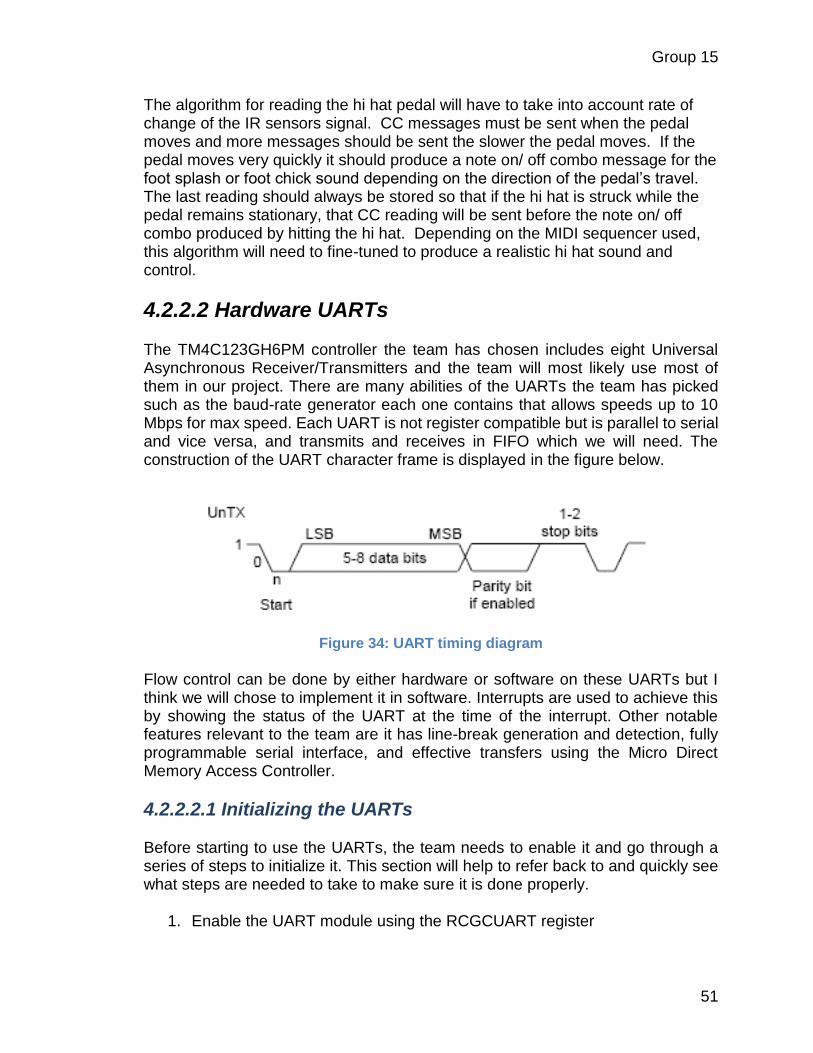
Group 15
51
The algorithm for reading the hi hat pedal will have to take into account rate of change of the IR sensors signal. CC messages must be sent when the pedal moves and more messages should be sent the slower the pedal moves. If the pedal moves very quickly it should produce a note on/ off combo message for the foot splash or foot chick sound depending on the direction of the pedal’s travel. The last reading should always be stored so that if the hi hat is struck while the pedal remains stationary, that CC reading will be sent before the note on/ off combo produced by hitting the hi hat. Depending on the MIDI sequencer used, this algorithm will need to fine-tuned to produce a realistic hi hat sound and control.
4.2.2.2 Hardware UARTs The TM4C123GH6PM controller the team has chosen includes eight Universal Asynchronous Receiver/Transmitters and the team will most likely use most of them in our project. There are many abilities of the UARTs the team has picked such as the baud-rate generator each one contains that allows speeds up to 10 Mbps for max speed. Each UART is not register compatible but is parallel to serial and vice versa, and transmits and receives in FIFO which we will need. The construction of the UART character frame is displayed in the figure below.
Figure 34: UART timing diagram
Flow control can be done by either hardware or software on these UARTs but I think we will chose to implement it in software. Interrupts are used to achieve this by showing the status of the UART at the time of the interrupt. Other notable features relevant to the team are it has line-break generation and detection, fully programmable serial interface, and effective transfers using the Micro Direct Memory Access Controller.
4.2.2.2.1 Initializing the UARTs Before starting to use the UARTs, the team needs to enable it and go through a series of steps to initialize it. This section will help to refer back to and quickly see what steps are needed to take to make sure it is done properly.
1. Enable the UART module using the RCGCUART register

Group 15
52
2. Enable the clock to the appropriate GPIO module via the RCGCGPIO register
3. Set the GPIO AFSEL bits for the appropriate pins 4. Configure the GPIO current level and/or slew rate as specified for the mode
selected 5. Configure the PMCn fields in the GPIOPCTL register to assign the UART
signals to the correct pins
4.2.2.3 The Open Source FAT File System/ SD Card Library The SD library allows for reading from and writing to SD cards. The library supports FAT16 and FAT32 file systems on standard SD cards which is just what the team needs for this system. The file names passed to the SD library functions can include paths separated by forward-slashes for example "directory/filename.txt". Because the working directory is always the root of the SD card, a name refers to the same file whether or not it includes a leading slash. SD memory card uses SPI bus. Using the provided library, all the SPI parameters are automatically set. User should only write in firmware what Flyport pins are connected to SD card connector, using the function SDInit. If the SD card is not connected with the correct pins the team won’t be able to use the library. The team will need to find an SD card library that works well with what we are trying do to. Writing our files to the SD card will be a one-time thing, so we will not need library functions for that purpose. However reading and communicating with the SD card quickly and effectively is a must for us, so predefined functions in a SD library that do this is what we are looking for. Functions like position(), seek(), size(), isDirectory(), close() etc is what we need. Luckily for us there is an abundance of open source code and examples for the FAT file system regarding embedded systems using microcontrollers much like ours. Implementing the two will prove to be rewarding when we have all he functions at our disposal.
4.2.2.3.1 Reading from the SD Card
It is important to note that before the team can read and write data to the SD card. It must be initialized first which requires going through some important steps. Assuming that power is on, the list goes as follows:
Make sure clock speed is at or less than 400kHz Hold CS line low and send some manual clock pulses CS line too is held high to show there is communication Send the reset command (CMD0) Wait for the SD card to respond with 0x01 Send initialize command (CMD1)

Group 15
53
Continue sending CMD1 until card responses with 0x00 Set sector size to 512 bytes each (CMD16) Turn off the CRC by sending CMD59 (now we no longer need to use CRC
values)
Now, when the card responds a final time, it has finally been initialized!
4.2.2.3.2 Improving the Speed of Reading from the SD Card Reading and writing from our external memory device that has all of our wav files stored on it is very important. We need this process to be as quick as possible in order to reduce the latency when we need to call our card and playback a sound the user has requested. There are a few ways to increase this read speed that we have been researching. One way is that if you have an SD card with cache, you can adjust the amount of cache used by the card and significantly increase read speeds. You must modify the amount of available read-ahead cache for reading SD Card data. By default, most ROMs will have anywhere from 4KB up to 128KB. This approach is used by a lot of android users but may have a lot of effect on our embedded system. Further research showed that newer SD cards can improve reading and writing speed by increasing the bus rate which is the frequency of the clock signal that grabs all the information the team needs from the card. With this functionality the card goes into a state where it is not disturbed or interrupted until the read or write is complete. With either of these methods, if we can get to a speed of about 20 Mbps we can achieve what we want for playback.
4.2.2.3.3 A First In First Out (FIFO) Buffer for smooth Audio Playback Because the SD card can only send data to the MCU in chunks and because there is some amount of time it take to receive each chunk, A FIFO buffer will need to written. Without using a FIFO, the audio playback would be glitchy and no fun to listen to. This buffer will keep sound production going while the MCU is retrieving a new chunk of data. Also because Glove Drummer will mix audio files, several FIFOs may be used.
4.2.2.4 Mixing Digital Audio Samples Glove Drummer will need to be able to create multiple sounds at once since the user will be simulating playing the drums. To do this our hardware and software will have to handle many audio playbacks being requested at once, and our speaker will have to play back all of these. This will require us to mix the audio samples together, the most important stage being the mixing of the digital audio, but before doing so it needs to be understood at a sound wave level. Mixing two sound waves is basically observing their interference (source7). When waves hit

Group 15
54
each other, they can interfere constructively or destructively. That is, when wave crests come together, a crest and a valley cancel each other out and two valleys form a bigger valley. More complex sounds, like music or speech, are merely the result of mixing sound waves of different frequencies, but we will be mixing many short, around 2 seconds, drum audio sounds. We don’t want these sounds to play as one and mess together, but for them to play independently of each other. With Digital audio mixing it is hard to avoid overflowing and clipping. When mixing it is important to keep the dynamics of each sound intact as much as possible and for this we will need a good algorithm in our code. If it isn’t correct one sound may be doubled in noise while the other is much quieter so it’s important we find the right algorithm for our system. There are 3 important things to note when analyzing how we are going to mix. They are quoted from a great source:
1. “If both samples are positive, we mix them so that the output value is somewhere between the maximum value of the two samples, and the maximum possible value”
2. “If both samples are negative, we mix them so that the output value is somewhere between the minimum value of the two samples, and the minimum possible value”
3. “If one sample is positive, and one is negative, we want them to cancel out somewhat”
4.2.2.5 PCM to PWM Conversion: Driving the Speaker For our software and the way the team has created the first design of the system using Pulse Width Modulation to drive the speakers. However all the hardware is designed to take Pulse Code Modulation (PCM) and it is usually what form the digital input is. We will need to make sure the conversion from PCM to PWM is smooth and without issues. The first step is for a digital amplifier to do digital conversion on a PCM digital input into PWM. The PWM modulator then makes a high voltage signal which needs to be filtered to recreate the original audio input. The reconstruction of this signal is very important, so the time alignment of the wave and the voltage needs to be noted. The PWM signal is generated digitally and s pulse widths are quantized. Also we need to make sure resolution in the PWM waveform is dependent of the ratio of the Master Clock frequency to know we are on the right path. Digital amplifiers must have the following: Power supply purity and impedance, PWM switching speed and resolution, and Master Clock frequency. We are choosing PWM mainly because of the FPGA we are producing because it will work very well with it. With our designed FPGA we can run a couple hundred MHz and it will have plenty of available multiplier blocks to use. A graphical representation of PCM to PWM conversion is show in the figure below.
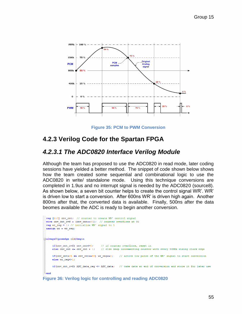
Group 15
55
Figure 35: PCM to PWM Conversion
4.2.3 Verilog Code for the Spartan FPGA
4.2.3.1 The ADC0820 Interface Verilog Module Although the team has proposed to use the ADC0820 in read mode, later coding sessions have yielded a better method. The snippet of code shown below shows how the team created some sequential and combinational logic to use the ADC0820 in write/ standalone mode. Using this technique conversions are completed in 1.9us and no interrupt signal is needed by the ADC0820 (source8). As shown below, a seven bit counter helps to create the control signal WR’. WR’ is driven low to start a conversion. After 600ns WR’ is driven high again. Another 800ns after that, the converted data is available. Finally, 500ns after the data beomes available the ADC is ready to begin another conversion.
Figure 36: Verilog logic for controlling and reading ADC0820

Group 15
56
4.2.3.2 The UART Verilog Module To start the process of building the hand modules, an open source Verilog module from OpenCores.org was used to send single byte messages to RealTerm terminal software on a PC. This UART module required a one clock pulse signal to latch data into its shift register and begin transmitting. For generating a one clock cycle pulse, a push button was used. Because the push button bounces and is asynchronous to the clock it has to be “debounced” before using it to trigger the transmission of a message. The code written to debounce the push button counted the number of times the push button signal bounced between zero and one, and after 32,768 bounces the signal PB_down was asserted for one clock cycle only. From this point, PB_down was used to start the transmission of a single byte. Tests using RealTerm showed the proper transmission of 0xD6 with each press of the push button. Using the running status technique mentioned in Section 2.1, a single press of the push button would need to trigger five separate one byte messages. These five bytes are what is required to turn a note on and then off with the MIDI protocol. Of course a pushbutton does not give any velocity information, but the team felt that velocity sensitivity would not be a far leap from using a push button to trigger fixed velocity drum sounds. In order to create five separate one clock cycle pulses and to latch the correct data into the UART’s shift register, a new state machine was created. It included and idle state as well as a state for transmitting each of the five bytes, as shown in the figure below. The process of sending the five bytes began with the assertion of the synchronous, debounced PB_down signal. After this time, the state machine cycled through the next five states and then returned to the MSG_IDLE state. A shift register and some combinational logic was then used to create a one clock cycle pulse with each change of state as shown in the figure below containing Verilog code.

Group 15
57
Figure 37: State Machine for sending five bytes from the UART at PB_down
Figure 38: Logic for creating a one clock cycle pulse with each change of state
4.2.3.3 The Peak Detection Verilog Module After successfully sending some fixed velocity MIDI messages and learning to control and read the ADC0820, the time came to implement a velocity sensitive MIDI controller. This sequence is a very good example of using the divide and conquer method. A state machine designed by the Glove Drummer team for finding the peak of a single piezo signal is shown below. Two timers are involved with this state machine. The first timer decides how long to search for a peak after the piezo signal breaks a preset threshold parameter. The second timer stalls the system for a period of time in order to prevent unwanted double triggering of the drum sound. These timers are parameterized and can be easily tuned to give a low latency, responsive feel to playing a single drum. When the state machine transitions from SEND to HOLD, a one clock cycle pulse begins sending a running status MIDI message. The peak value has already been assigned to data2_on when message transmission is initiated. Later more sensors will be added and the five byte messages will be stripped down to two bytes that will be sent wirelessly.
Group 15
58
Figure 39: Verilog State Machine for Peak Detection
4.2.4 Hex Editor Software If the team decides against using a files system on the SD Card, then a Hex Editor will be needed. A Hex Editor simply allows the user to manage and change hexadecimal values of our wav files. It is a software program that can manipulate binary data that will eventually run computer files. The editor can parse and edit data on sectors straight from the physical SD card. Its mainly for viewing and editing the exact contents of the file, without changing the structure of the file format. If something goes wrong with our system and we need to make a slight alteration to one of our files in the editor, we can go inside the file and correct corrupted data, or set up exception handling since our system is structured slightly different than usual and may throw some unwanted errors. In our Hex Editor the data of the computer file is represented as hexadecimal values grouped in 4 groups of 4 bytes, followed by one group of 16 ASCII characters which are derived from each pair of hex values. In the figure below, we can see a brief example of how a file would be structured in the Hex editor, and it is important for us understand how to edit it. It closely resembles the file allocation table format, which makes sense since this will be used to work with our SD card that is in the FAT file system. Another strength with our editor is that it will use a template system to structure our file to the format we choose. This is helpful for code generation because you can enter variable type, decimal number or offset and the basic layout will be made.
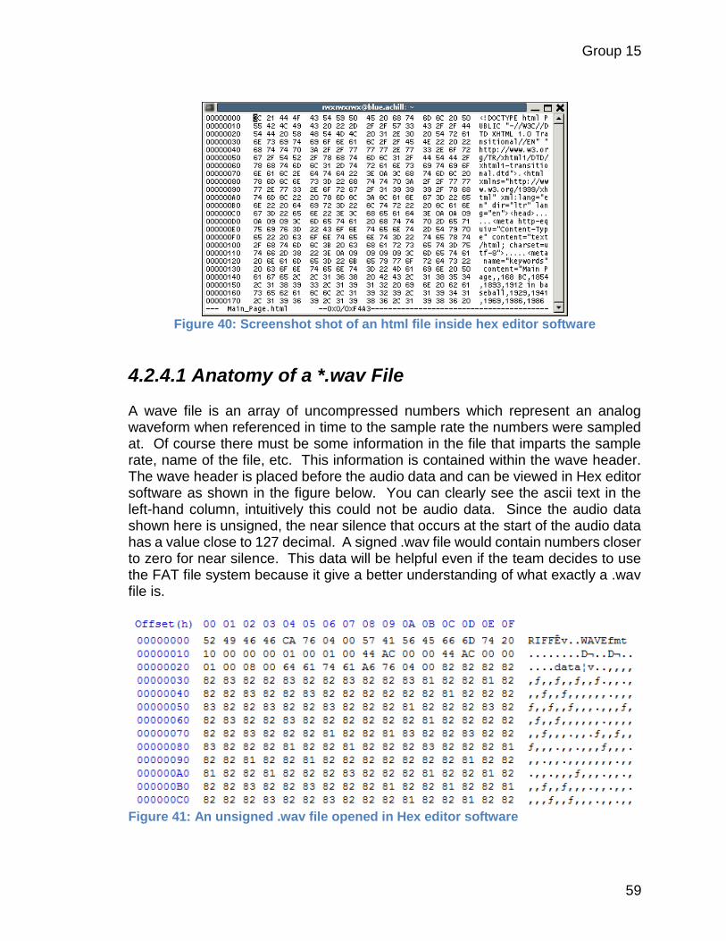
Group 15
59
Figure 40: Screenshot shot of an html file inside hex editor software
4.2.4.1 Anatomy of a *.wav File A wave file is an array of uncompressed numbers which represent an analog waveform when referenced in time to the sample rate the numbers were sampled at. Of course there must be some information in the file that imparts the sample rate, name of the file, etc. This information is contained within the wave header. The wave header is placed before the audio data and can be viewed in Hex editor software as shown in the figure below. You can clearly see the ascii text in the left-hand column, intuitively this could not be audio data. Since the audio data shown here is unsigned, the near silence that occurs at the start of the audio data has a value close to 127 decimal. A signed .wav file would contain numbers closer to zero for near silence. This data will be helpful even if the team decides to use the FAT file system because it give a better understanding of what exactly a .wav file is.
Figure 41: An unsigned .wav file opened in Hex editor software
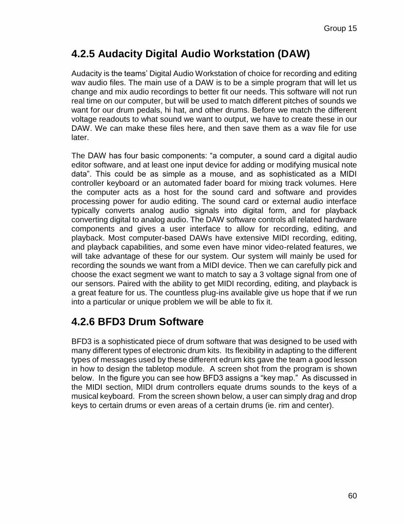
Group 15
60
4.2.5 Audacity Digital Audio Workstation (DAW) Audacity is the teams’ Digital Audio Workstation of choice for recording and editing wav audio files. The main use of a DAW is to be a simple program that will let us change and mix audio recordings to better fit our needs. This software will not run real time on our computer, but will be used to match different pitches of sounds we want for our drum pedals, hi hat, and other drums. Before we match the different voltage readouts to what sound we want to output, we have to create these in our DAW. We can make these files here, and then save them as a wav file for use later. The DAW has four basic components: “a computer, a sound card a digital audio editor software, and at least one input device for adding or modifying musical note data”. This could be as simple as a mouse, and as sophisticated as a MIDI controller keyboard or an automated fader board for mixing track volumes. Here the computer acts as a host for the sound card and software and provides processing power for audio editing. The sound card or external audio interface typically converts analog audio signals into digital form, and for playback converting digital to analog audio. The DAW software controls all related hardware components and gives a user interface to allow for recording, editing, and playback. Most computer-based DAWs have extensive MIDI recording, editing, and playback capabilities, and some even have minor video-related features, we will take advantage of these for our system. Our system will mainly be used for recording the sounds we want from a MIDI device. Then we can carefully pick and choose the exact segment we want to match to say a 3 voltage signal from one of our sensors. Paired with the ability to get MIDI recording, editing, and playback is a great feature for us. The countless plug-ins available give us hope that if we run into a particular or unique problem we will be able to fix it.
4.2.6 BFD3 Drum Software BFD3 is a sophisticated piece of drum software that was designed to be used with many different types of electronic drum kits. Its flexibility in adapting to the different types of messages used by these different edrum kits gave the team a good lesson in how to design the tabletop module. A screen shot from the program is shown below. In the figure you can see how BFD3 assigns a “key map.” As discussed in the MIDI section, MIDI drum controllers equate drums sounds to the keys of a musical keyboard. From the screen shown below, a user can simply drag and drop keys to certain drums or even areas of a certain drums (ie. rim and center).
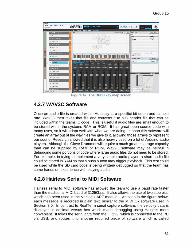
Group 15
61
Figure 42: The BFD3 key map screen
4.2.7 WAV2C Software Once an audio file is created within Audacity at a specifici bit depth and sample rate, Wav2C then takes that file and converts it to a C header file that can be included within the teams’ C code. This is useful if audio files are small enough to be stored within the systems RAM or ROM. It has great open source code with many uses, so it will adapt well with what we are doing. In short this software will create an array out of the wav files we give to it, allowing those arrays to represent our sound. Research showed that it is also heavily used on a lot of Arduino audio players. Although the Glove Drummer will require a much greater storage capacity than can be supplied by RAM or ROM, Wav2C software may be helpful in debugging some portions of code where large audio files do not need to be stored. For example, in trying to implement a very simple audio player, a short audio file could be stored in RAM so that a push button may trigger playback. This test could be used while the SD card code is being written/ debugged so that the team has some hands on experience with playing audio.
4.2.8 Hairless Serial to MIDI Software Hairless serial to MIDI software has allowed the team to use a baud rate faster than the traditional MIDI baud of 31250bps. It also allows the use of two stop bits, which has been used in the Verilog UART module. As seen in the figure below, each message is recorded in plain text, similar to the MIDI Ox software used in Section 3.0. In contrast to RealTerm serial capture software, the velocity data is displayed in decimal versus hex which made debugging using Hairless more convenient. It takes the serial data from the FT232, which is connected to the PC via USB, and routes it to another required piece of software which is called
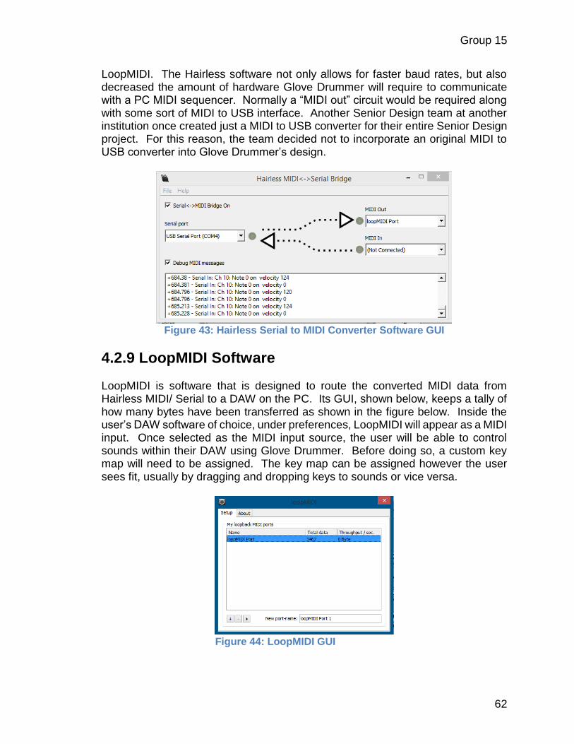
Group 15
62
LoopMIDI. The Hairless software not only allows for faster baud rates, but also decreased the amount of hardware Glove Drummer will require to communicate with a PC MIDI sequencer. Normally a “MIDI out” circuit would be required along with some sort of MIDI to USB interface. Another Senior Design team at another institution once created just a MIDI to USB converter for their entire Senior Design project. For this reason, the team decided not to incorporate an original MIDI to USB converter into Glove Drummer’s design.
Figure 43: Hairless Serial to MIDI Converter Software GUI
4.2.9 LoopMIDI Software LoopMIDI is software that is designed to route the converted MIDI data from Hairless MIDI/ Serial to a DAW on the PC. Its GUI, shown below, keeps a tally of how many bytes have been transferred as shown in the figure below. Inside the user’s DAW software of choice, under preferences, LoopMIDI will appear as a MIDI input. Once selected as the MIDI input source, the user will be able to control sounds within their DAW using Glove Drummer. Before doing so, a custom key map will need to be assigned. The key map can be assigned however the user sees fit, usually by dragging and dropping keys to sounds or vice versa.
Figure 44: LoopMIDI GUI

Group 15
63
5.0 Prototyping
5.1 Construction of Piezo Sensors Starting with 9.5mm diameter piezoelectric transducers the Glove Drummer team successfully created a sensor that would fit on the fingertip and create a quick voltage response to mechanical vibration. The voltage response was shown in Section 5.1 to die out long before the finger would have a chance to make a subsequent tap on the table. Other glove controllers have used different types of sensors including force sensitive resistors and piezo films, but the team feels that these piezo discs are superior. Cost alone makes them a better choice as they can purchased in lots of 50 for $35. It is a wonder that no other glove controllers for the drums have used them, since all electronic drum kits use piezos. The bare piezo sensor contains a thin piezoelectric ceramic disc attached to a thin brass disk. An anode is applied is applied to the top side of the ceramic disk while the bottom side ties the cathode to the brass disk. Wires stripped from USB cables were chosen to connect to the sensors because of their small diameter and availability. Wires had to be carefully soldered to the tiny piezo disk. The process of soldering these connections also had to be done very quickly so that the Curie point of the ceramic disk was not exceeded for too long. citation If the Curie point of any piezoelectric material is exceeded for too long, that material will lose its piezoelectric properties and no longer generate any sort of voltage response. Once the wires were soldered into place, the team came to the realization that the solder joints were actually stronger than the bare piezo disk itself. Strong hits against the table would therefore cause the solder joint to bend the brass disk and crack the ceramic disk on top. Luckily the team found some 1.0mm brass disks that are much stronger than the brass disk of the bare piezo. These slightly larger brass disks were then glued to the bare piezo disk for reinforcement. For additional protection, the team added a 1.0mm foam rubber disk on the top side of the bare piezo to finish Glove Drummer’s fingertip sensors.
Figure 45: Bare piezo transducers (front and back) and finished sensors (front and back)
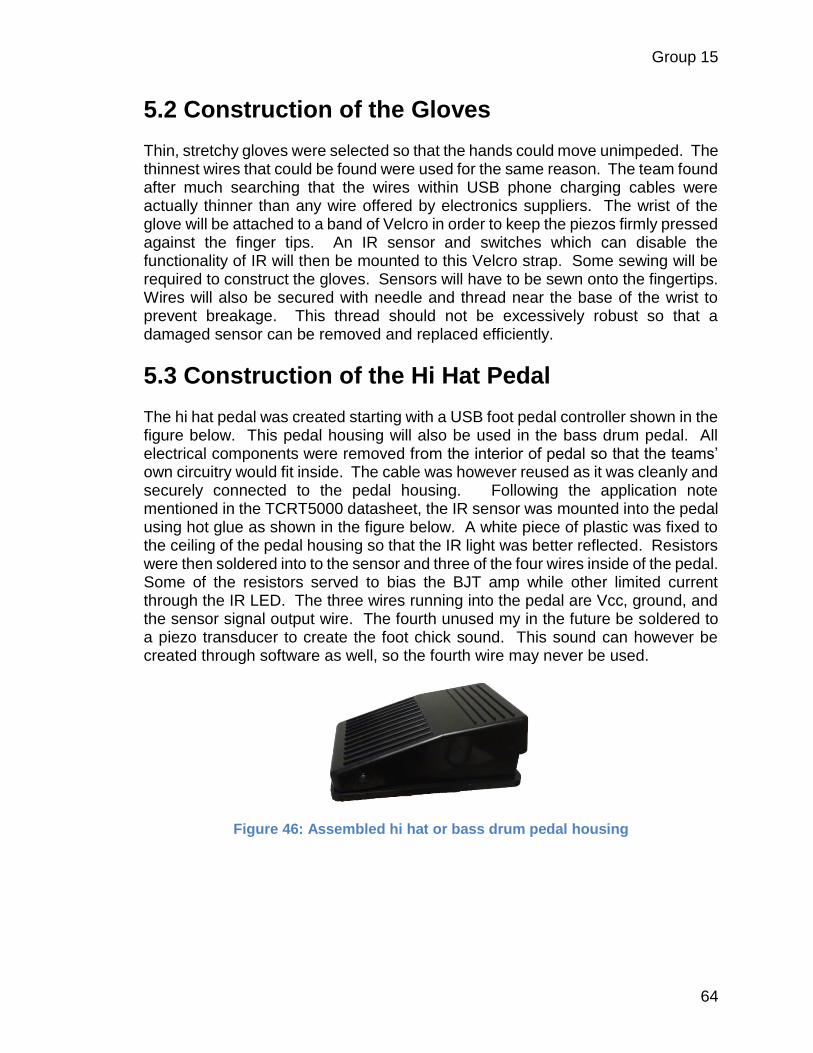
Group 15
64
5.2 Construction of the Gloves Thin, stretchy gloves were selected so that the hands could move unimpeded. The thinnest wires that could be found were used for the same reason. The team found after much searching that the wires within USB phone charging cables were actually thinner than any wire offered by electronics suppliers. The wrist of the glove will be attached to a band of Velcro in order to keep the piezos firmly pressed against the finger tips. An IR sensor and switches which can disable the functionality of IR will then be mounted to this Velcro strap. Some sewing will be required to construct the gloves. Sensors will have to be sewn onto the fingertips. Wires will also be secured with needle and thread near the base of the wrist to prevent breakage. This thread should not be excessively robust so that a damaged sensor can be removed and replaced efficiently.
5.3 Construction of the Hi Hat Pedal The hi hat pedal was created starting with a USB foot pedal controller shown in the figure below. This pedal housing will also be used in the bass drum pedal. All electrical components were removed from the interior of pedal so that the teams’ own circuitry would fit inside. The cable was however reused as it was cleanly and securely connected to the pedal housing. Following the application note mentioned in the TCRT5000 datasheet, the IR sensor was mounted into the pedal using hot glue as shown in the figure below. A white piece of plastic was fixed to the ceiling of the pedal housing so that the IR light was better reflected. Resistors were then soldered into to the sensor and three of the four wires inside of the pedal. Some of the resistors served to bias the BJT amp while other limited current through the IR LED. The three wires running into the pedal are Vcc, ground, and the sensor signal output wire. The fourth unused my in the future be soldered to a piezo transducer to create the foot chick sound. This sound can however be created through software as well, so the fourth wire may never be used.
Figure 46: Assembled hi hat or bass drum pedal housing
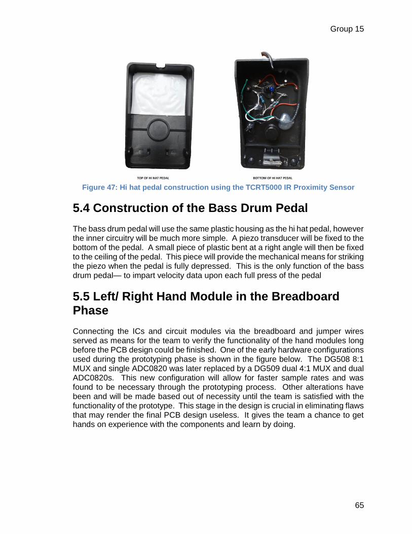
Group 15
65
Figure 47: Hi hat pedal construction using the TCRT5000 IR Proximity Sensor
5.4 Construction of the Bass Drum Pedal The bass drum pedal will use the same plastic housing as the hi hat pedal, however the inner circuitry will be much more simple. A piezo transducer will be fixed to the bottom of the pedal. A small piece of plastic bent at a right angle will then be fixed to the ceiling of the pedal. This piece will provide the mechanical means for striking the piezo when the pedal is fully depressed. This is the only function of the bass drum pedal— to impart velocity data upon each full press of the pedal
5.5 Left/ Right Hand Module in the Breadboard Phase Connecting the ICs and circuit modules via the breadboard and jumper wires served as means for the team to verify the functionality of the hand modules long before the PCB design could be finished. One of the early hardware configurations used during the prototyping phase is shown in the figure below. The DG508 8:1 MUX and single ADC0820 was later replaced by a DG509 dual 4:1 MUX and dual ADC0820s. This new configuration will allow for faster sample rates and was found to be necessary through the prototyping process. Other alterations have been and will be made based out of necessity until the team is satisfied with the functionality of the prototype. This stage in the design is crucial in eliminating flaws that may render the final PCB design useless. It gives the team a chance to get hands on experience with the components and learn by doing.
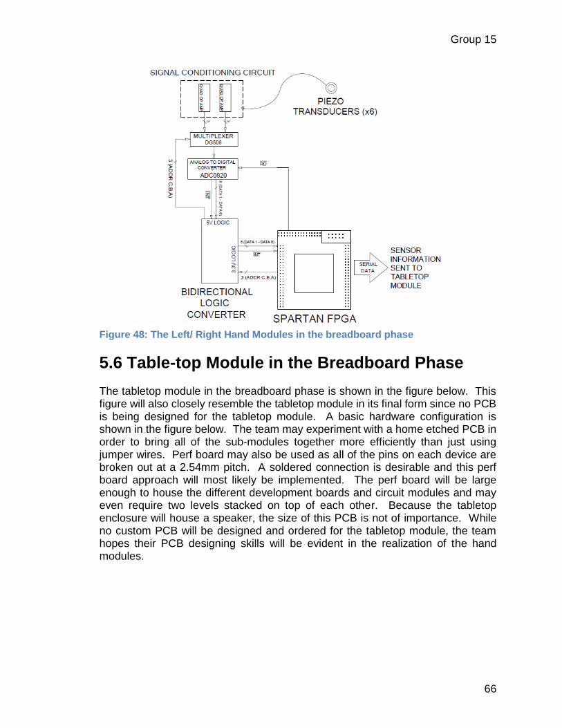
Group 15
66
Figure 48: The Left/ Right Hand Modules in the breadboard phase
5.6 Table-top Module in the Breadboard Phase The tabletop module in the breadboard phase is shown in the figure below. This figure will also closely resemble the tabletop module in its final form since no PCB is being designed for the tabletop module. A basic hardware configuration is shown in the figure below. The team may experiment with a home etched PCB in order to bring all of the sub-modules together more efficiently than just using jumper wires. Perf board may also be used as all of the pins on each device are broken out at a 2.54mm pitch. A soldered connection is desirable and this perf board approach will most likely be implemented. The perf board will be large enough to house the different development boards and circuit modules and may even require two levels stacked on top of each other. Because the tabletop enclosure will house a speaker, the size of this PCB is not of importance. While no custom PCB will be designed and ordered for the tabletop module, the team hopes their PCB designing skills will be evident in the realization of the hand modules.

Group 15
67
Figure 49: The Tabletop Module in the breadboard phase
5.6.1 Sub-Modules Since the tabletop module will house a speaker which needs to housed inside a large enclosure, the team has decided there is no need to design a compact PCB for the circuits contained in this module. Some circuits built by the team will be assembled on perf board and soldered for robust connections. Other circuits requiring surface mounted devices (SMD) will designed in eagle and etched from copper clad boards so that the surface mount pins can be broken out for access to jumper wires. The Tiva C dev board, the ATmega88 dev board, the SD card module, the wireless modules, and the analog conditioning circuit will all be connected either by jumper wires or by a large home-etched PCB. In the case that the team has time to etch this large PCB, all other smaller modules will plug into the large PCB to make the connection between them. In addition to the components mentioned here, the tabletop module may include another FPGA dev board if needed to reduce latency. It remains to be seen that the Tiva C will be able to sample the pedals, read incoming serial data from the hands, output MIDI messages to a PC, and drive the speakers from the SD card. Since the Waveshare FPGA board costs only $35 and since it has already been used in the hand modules, this may be advantageous in reducing latency.
5.6.1.1 Power Supply No AC to DC conversion will occur within the tabletop module because of the abundance of AC to DC converters today. The team feels that many users may already own a suitable power supply at home that will work with the use of linear DC to DC voltage regulators within the tabletop module. A wall wart supply with a minimum current capability of 500mA operating at a voltage between 7V and 15V should be suitable. A 7805 IC will then create the 5V supply rail. The Tiva C’s onboard 3.3V regulator will bring the 5V supply down to 3.3V to be used by the

Group 15
68
rest of system including the SD card and the wireless modules. Sufficient current must be supplied to these components and may require an additional 3.3V regulator. This additional regulator, if required, will be soldered to perf board and mounted with the rest of the circuit modules to the speaker enclosure. As usual the supply will be filtered so that each circuit receives a stable supply or reference voltage without excessive ripple.
5.6.1.2 Atmega88 MCU (3.3V) The ATmega88 may not be required in the tabletop module if the wireless modules are connected directly to the Tiva C. There are advantages and disadvantages to using this MCU between the Tiva C and wireless modules. Advantages include only having to implement one NRF24L01 SPI library and less tasks assigned to the Tiva C so that audio quality/ latency may be improved. One disadvantage is the added cost of the additional MCUs.
5.6.1.3 NRF24L01 Module The NRF24L01 will be connected to the SPI port of the Tiva C to accept messages from hand modules. Shown in the figure below, the module will be connected either directly to the Tiva C to the ATmega88 which will relay data to the Tiva C as discussed in the precious section. Female headers will be soldered to the perf mother board so that these modules will simply plug in.
Figure 50: The NRF24L01 Wireless Module
5.6.1.4 SD Card Module To connect an SD card to our Tiva C Series microcontroller Glove Drummer will require an SD card Module that is connected with the correct pin assignments. SD cards of any size can be used with ease. Note that the mainboard has to support the FAT file system. Our Tiva C series supports the FAT file system so the team doesn’t need to worry about that. This kind of SD module makes use of the SPI based (1-bit bus) to access the memory card. They also include a 3.3v regulator chip on-board (the same as our microcontroller) so we can supply +5v if we need to. This gives us a simple way to connect/disconnect our SD card and know that is it connected to our system correctly. Below is the SD card module the team has

Group 15
69
decided on for our project, and it has plenty of documentation to provide a smooth integration.
Figure 51: SD Card Logging Shield to be connected to Tiva C
5.6.1.5 Bass Drum Pedal Piezo Conditioning Circuit One of the analog input pins of the Tiva C will need to be connected to the circuit shown in the figure below. Since the Tiva C is a 3.3V MCU, the opamp will be biased with 3.3V opposed to 5V. This circuit is the same one that is being used in the hand modules as the bass drum pedal uses the same piezo sensors. A piezo sensor will be mounted in the bottom of the pedal housing. The top of the pedal housing will have an attached piece of plastic bent at a right angle. This piece of plastic will strike the bass drum pedal piezo when the pedal is full depressed. A similar approach may be used in the hi hat controller pedal in order to generate to the foot splash sound.
Figure 52 : First prototype bass drum pedal conditioning circuit on perf board
Group 15
70
5.6.1.6 Audio Amplifier Circuits The tabletop modules headphone and speaker amplifier circuits will be built onto perf board as well. The OPA134 will be used in conjunction with metal film resistors and capacitors. Connections to the Tiva Cs PWM port will be made via the header pins. A panel mount 1/8th inch jack will facilitate the connection of the headphones. This headphone jack is a “switched” type jack which detects the insertion of the headphones and opens a switch. When this switch is opened, the PWM signal will be routed to the headphone amp circuit rather than the speaker amp circuit. Panel mount logarithmic potentiometers will allow for volume adjustment of the headphones and speaker.
5.6.1.7 Tabletop Module I/O All data input to the tabletop module will be obtained wirelessly through the NRF24L01 module. Data outputs of the tabletop module include the speaker and the headphone output jack. The headphone output jack is a “switched” type jack which allows for the speaker amplifier circuit to be bypassed upon insertion of the headphones. As for power input to the tabletop module, a simple PCB mount barrel jack connector will be used.
6.0 Piezo Signal Conditioning
6.1 The Unconditioned Piezo Signal In planning the piezo conditioning circuit, the Tektronix Digital Storage storage oscilloscope (scope) was used to view the pulses generated by striking the piezo against the table. The sensors were fastened to the index fingertip of the glove and the resulting signal was observed on the scope. The proper trigger setting had to be determined in order to properly capture the pulses. These trigger settings were documented for future work with the sensors and oscilloscope. The sensor, which is made up of a 9.5mm piezo transducer sandwiched in between a brass disk and a foam rubber disk, creates an AC voltage when the piezo crystal inside is deformed. Positive and Negative pulses are produced as the piezo crystal reverberates as shown in the figure below. Additionally, the force exerted in striking the sensor against the table is proportional the peak magnitudes of those pulses. This is a very important characteristic for the sensor to have since Glove Drummer will play back different drum sounds for a certain drum hit with varying force. Surprisingly, the peak voltages were lower than expected based on electronic drum projects using larger piezo sensors. The team reasoned that since the size of the piezo crystal used here is smaller than in those projects, the resulting voltage waveform would also be smaller.

Group 15
71
Exceptionally hard hits of the sensor against the table resulted in clipping on the scope which could mean a few different things. One is that the sensor is simply not meant to be struck this hard and more padding should be added to the overall sensor design. Other theories are that the rise time was too fast or the peak was too high for scope to capture. In either case, not striking the sensors “too hard” and clamping the sensor signal to +Vref = 5V or 3.3V, depending on which ADC is used, will be a good idea. Of course the negative portions of the signal will need to be rectified as well in order to interface the sensors to one the ADCs available to the team.
Figure 53: The Tabletop Module in the breadboard phase
In addition to evaluating the magnitudes of the waveforms generated during a strike of the sensor, the length of the response was also noted. In Figure below, a waveform resulting from striking the index fingertip sensor repeatedly against the table at the fastest speed attainable by the members of the team is shown. Each individual strike of the sensor creates a pulse that dies out long before the next strike of the sensor. This is a very important characteristic for the sensor to have since users will be tapping their fingers very quickly at times. The ~150ms time period in between strikes correlates to about a 400 beat per minute (bpm) tempo for a single finger tap. Therefore with two fingers tapping alternately, a “drum roll” of approximately 800 bpm in tempo should be achievable. Also, noting the 150ms period between strikes will be useful in “debouncing” the sensor. Some strikes produce unwanted spikes in voltage long after the initial pulse. This would result in a “double trigger” where the drum sound plays more than once resulting in a machine gun type sound. This double trigger effect could be avoided using a counter that counts to 150ms after a valid strike before it allows another valid strike message to be sent. These preliminary tests proved to the team that while this exact sensor design has never been used in glove controllers, it could be very effective.

Group 15
72
Figure 54: Time in between pulses produced by fastest single-finger tap possible
6.2 The Piezo Conditioning Circuit
6.2.1 Op Amp Selection Since the piezo transducer has a high output impedance, amplification is necessary. Viewing the scope screen shots of the piezo sensors illustrated the need to rectify and clamp the sensor signal but did not account for the high impedance setting of the oscilloscope. The input specifications of the ADCs available to the team all include a max value for the output impedance of what is connected to the ADC. For this reason, JFET op amps were an obvious choice because of their high input impedance. The differential pair found at the input of these JFET op amps are made with transistors that are a mixture of BJTs and MOSFETs. This will result in a higher input impedance than if a standard BJT differential pair was used. Another figure of merit in selecting an appropriate op amp was the range of voltages available to DC bias the chip. A “single-supply” op amp that can output voltages from rail to rail was desired for the ease of providing dc power. With a single-supply op amp, the negative DC supply terminal is connected ground and the positive DC terminal is connected to Vcc (Vcc = 5V in this case). This type of op amp operates solely off the regulated 5V power supply and ground with no negative DC bias needed. It is also desirable that the conditioned piezo signal will clip exactly at 5V, so the op amp should be able to drive output voltages from “rail to rail.” If an op amp cannot drive its output to the top rail of 5V, then the full zero to five volt range cannot be used and velocity sensitivity would be diminished. As cost is always an issue, no op amps costing more than a few dollars each will be considered. The current choices are dual and quad op amp
Group 15
73
Dual Inline Packages (DIPs) which will fit in the breadboard and not take up too much PCB real estate versus single op amp chips. Another important factor in selecting parts is that the team is able to obtain free samples. More expensive op amps based on CMOS transistors which consume less power and have even higher input impedance may be sampled at no cost. For this reason alone the team may choose to experiment with some more costly op amps and other higher priced ICs. A comparison of some of the op amps chosen is shown below. All of these ICs were chosen first based on if a DIP packages have been made so that the team could experiment with them in the breadboard. Table 5: Op Amp Comparisons
Part # Manufacturer Technology 5V Single Supply ? Rail to Rail ?
LM324 TI BJT N N
TL072 TI JFET, BJT N Y
AD822 Analog Devices JFET, BJT Y Y
OPA350 TI CMOS Y Y
The team’s final decision was to use the OPA350 op amp from TI. With CMOS technology, the analog conditioning circuitry will consume less power. The added cost of using CMOS transistors was of no concern since the team will be sampling the parts from TI. This a high performance, low voltage chip that may be excessive to use in this situation. If Glove Drummer went into production, a les expensive op amp might be chosen.
6.2.2 Bounding the Piezo Signal between Ground and Vcc The exact allowed range of input voltages to the ADC0820 chip are defined in the datasheet as -200mV to 4.8V where Vcc=5V. Figure below illustrates the effect of adding a simple 1n4148 diode in series with the positive piezo terminal for a light and a hard strike of the sensor against a table. The diode effectively removes the negative portion of the piezo signal, which is good for the ADC but may have some repercussions. If the first largest peak produced by the strike of the sensor was negative then the half wave rectifier circuit would discard the larger negative peak leaving the ADC to read the following smaller positive peak. It may be a good idea to use a full wave rectifier circuit in order to keep this negative peak information.

Group 15
74
Figure 55: Light and Medium strikes of the sensor after half-wave rectification
Some very hard strikes will still produce a peak voltage of >10V so this peak must be attenuated somehow before interfacing the sensors to the ADC. This is where the addition of a BAT85 Schottky diode can be of use. When placed between the signal and ground, it effectively limits the output voltage to 5V. The voltage will be limited furthermore by the addition of an op amp circuit which cannot amplify past its upper supply rail.
6.2.4 The Final Conditioning Circuit Design The final circuit for interfacing the piezos to the ADC is shown in the schematic figure below . This circuit was modeled after several circuits that have been built for the purpose of building an electronic drum kit. One in particular electronic drum project which very well documented was found at edrum.info (source_8). This circuit not only amplifies the signal, but also filters out the components of the signal that are far from the piezos resonant frequency. The pass band of this circuit is centered at 20Hz. Also shown below are screenshots of the fully conditioned signal. It should be noted that there is not a drastic difference in these signals when compared to the half wave rectified signals. This is because of the high input impedance of the oscilloscope. If the half wave rectified signal were fed into the ADC0820 the voltage drop across the piezos output impedance would reduce the signal's magnitude, resulting in reduced velocity sensitivity.

Group 15
75
Figure 56: The Piezo Conditioning Circuit
Figure 57: Screenshots of the Conditioned Piezo Signal
7.0 PCB Planning Planning the PCB design is an arduous process where small mistakes can cost dearly in both time and money. Having built most of the circuits on the breadboard, the team has the working knowledge of how to interconnect the different functional blocks. Designing a PCB is similar to imaging the wires and layout of the breadboarded design shrinking down to the smallest possible size. Pads and traces will be at scale almost too small for human eyes in some cases and parts will shrink as well. While the team has selected parts in DIP packages for prototyping, surface mount devices (SMDs) will be used on the PCB. This works out since DIP packages are becoming less popular and almost any DIP device will also be manufactured as SMD. Resistors and capacitors, like ICs, will also be SMD and will be chosen at the same power rating (1/4W) as the through hole resistors (Rs), diodes (Ds), and capacitors (Cs) used in the breadboards. As the power rating of an SMD R or C determines its size, if the power rating is found to be excessive it will be reduced. Some SMD Rs and Cs with very low power rating are even too small for the Glove Drummer team to solder by hand to the PCB. Therefore a happy medium between small size and a high enough power rating should be found when choosing SMD Rs, Cs, and Ds. The team has decided to focus their PCB efforts on the hand modules to reduce the bulkiness of the project enclosure mounted to the forearms. Careful planning

Group 15
76
of the overall size of the PCB will be taken into account in selecting a proper enclosure. The enclosure will be clear plastic so that status LEDs may be viewed without mounting them externally. Another reason to choose plastic for the enclosure is that the team worried a metal box would mean trouble for any type of wireless communication. The enclosure will also facilitate the connection to a 2.1mm PCB mount barrel jack for charging of an 18650 lithium ion battery as well as an opening for an on/ off switch. Sensor input wires will be connected with 2.54mm header pins so that sensors may be easily replaced if they are damaged in any way. A slot will routed from the enclosure near the wrist in order to connect the sensors to these header pins. Once designed in Eagle CAD software, the PCB design will be sent to Osh Park. Osh Park was is a good choice since the sell PCBs in lots of three and this project requires two identical PCBs. The extra PCB will be good to have as a backup in case of soldering difficulties. If the budget allows, a four layer PCB will be ordered. A four layer PCB will allow the PCB to be much smaller and the project enclosures strapped to the forearms to be even less bulky. Components will be soldered by reflow using a hot plate. Some components may also be soldered by hand. Because of the low cost and complexity of the Spartan FPGA development board, it will be plugged into the custom PCB. This development board has an unknown amount of layers which is greater than four and cannot be reproduced in the same footprint by the Glove Drummer team. The ability to simply plug in the FPGA board to the custom PCB will also mean reducing the overall footprint of the PCB. The clear project enclosure will fit the stacked boards with room to spare and the space underneath the FPGA can then be populated with traces and components. PCB mount female headers with a pitch of 2.0mm will be created in Eagle and spaced exactly to accommodate the 124 pins of the FPGA dev board.
7.1 Signal Integrity Anywhere high frequencies are transmitting through the copper traces on the Glove Drummer PCB are areas of concern for ringing. If input and output impedances are not matched properly, signals will reflect causing momentary overshoot of the proper logic level (ie 5V or 3.3V). This can lead to intermittent failures in the circuitry which can be even worse than complete failure when trying to find a solution. Input and output impedances can be properly matched by calculating the inductance for the area of a copper trace while considering the parasitic capacitances of the header pins. By calculating the correct component values required and implementing a “snubber circuit” impedances will be properly matched and intermittent failures can be avoided. Ground planes can also help by supplying some capacitance nearby hi frequency copper traces which can effectively eliminate the inductance of that trace. In the teams’ Embedded Systems course over the Summer of 2014, Dr. Weeks stressed the importance of signal integrity in hardware design. This information will be of great use to the team in avoiding some potential pitfalls of PCB planning.

Group 15
77
7.2 Custom PCB for Left/ Right hand Modules
7.2.1 Power Supply In designing the PCB, the team has planned for a wireless implementation of the hand modules. This meant including a portable power source. The 18650 lithium ion battery was chosen because of its high power desnity and relatively low cost. It was also chosen because of the wealth of information that exists about using these batteries. A solution had to be found that regulated the varying voltage that comes from these batteries. Lucky for the team, Texas Instruments has taken a lot of time to consider battery powered device design. The TPS line of ICs from T.I. were selected as they give the most complete power solution compared to other power management ICs. The BQ24074 is designed to charge a single 18650 lithium ion cell while at the same time powering the system. A boost DC to DC switching regulator is used to create a +5V supply rail. To create a +3.3V rail, a buck/ boost regulator will be used. These ICs have a special pad on their underside which is meant to be connected to “power ground.” This makes for three separate grounds that can be found in the Glove Drummer schematic. Each of these grounds will make use of a start pattern to return current from each respective component. All three of these grounds will all come together at one point as well.
Figure 58: Battery charger and voltage regulators for custom PCB
7.2.3 Integrated Circuits (ICs)
7.2.3.1 ICs Tied to Analog Ground
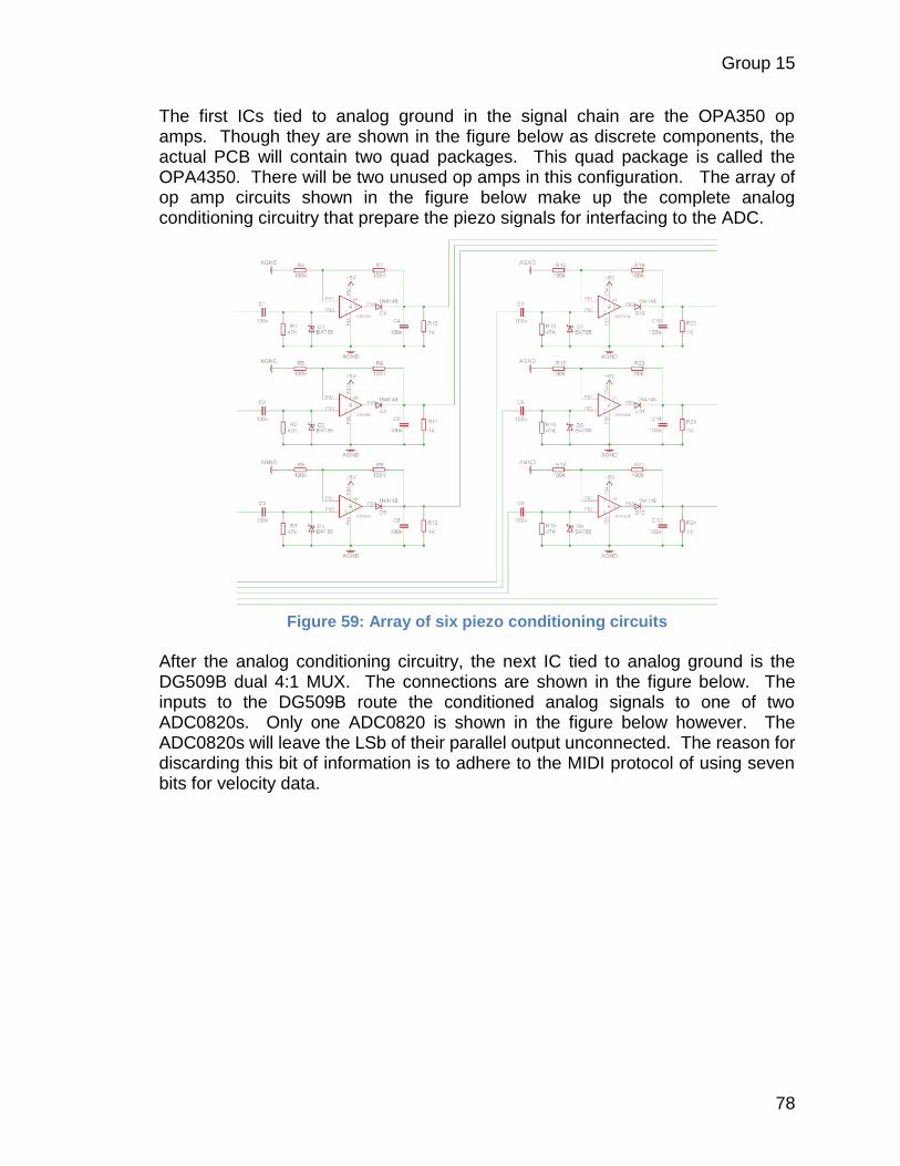
Group 15
78
The first ICs tied to analog ground in the signal chain are the OPA350 op amps. Though they are shown in the figure below as discrete components, the actual PCB will contain two quad packages. This quad package is called the OPA4350. There will be two unused op amps in this configuration. The array of op amp circuits shown in the figure below make up the complete analog conditioning circuitry that prepare the piezo signals for interfacing to the ADC.
Figure 59: Array of six piezo conditioning circuits
After the analog conditioning circuitry, the next IC tied to analog ground is the DG509B dual 4:1 MUX. The connections are shown in the figure below. The inputs to the DG509B route the conditioned analog signals to one of two ADC0820s. Only one ADC0820 is shown in the figure below however. The ADC0820s will leave the LSb of their parallel output unconnected. The reason for discarding this bit of information is to adhere to the MIDI protocol of using seven bits for velocity data.
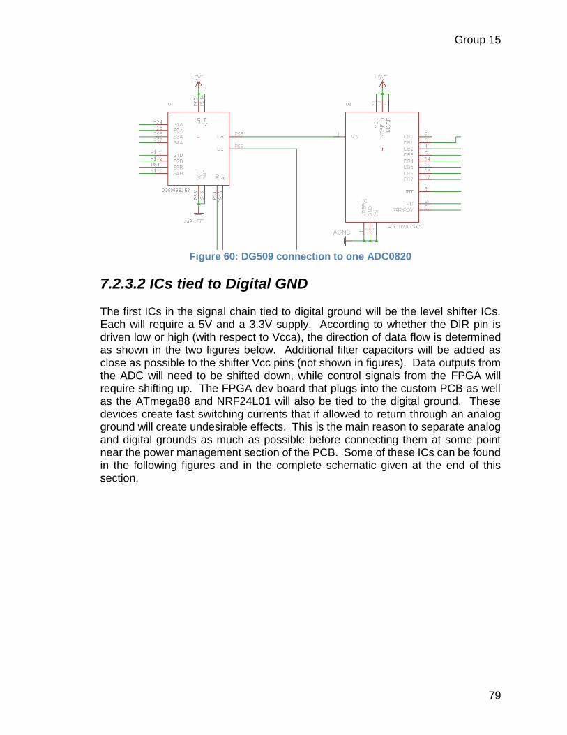
Group 15
79
Figure 60: DG509 connection to one ADC0820
7.2.3.2 ICs tied to Digital GND The first ICs in the signal chain tied to digital ground will be the level shifter ICs. Each will require a 5V and a 3.3V supply. According to whether the DIR pin is driven low or high (with respect to Vcca), the direction of data flow is determined as shown in the two figures below. Additional filter capacitors will be added as close as possible to the shifter Vcc pins (not shown in figures). Data outputs from the ADC will need to be shifted down, while control signals from the FPGA will require shifting up. The FPGA dev board that plugs into the custom PCB as well as the ATmega88 and NRF24L01 will also be tied to the digital ground. These devices create fast switching currents that if allowed to return through an analog ground will create undesirable effects. This is the main reason to separate analog and digital grounds as much as possible before connecting them at some point near the power management section of the PCB. Some of these ICs can be found in the following figures and in the complete schematic given at the end of this section.
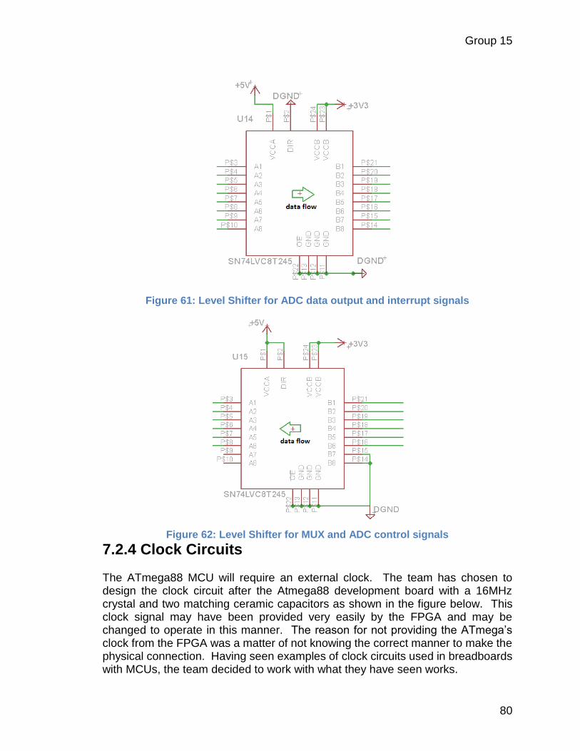
Group 15
80
Figure 61: Level Shifter for ADC data output and interrupt signals
Figure 62: Level Shifter for MUX and ADC control signals
7.2.4 Clock Circuits The ATmega88 MCU will require an external clock. The team has chosen to design the clock circuit after the Atmega88 development board with a 16MHz crystal and two matching ceramic capacitors as shown in the figure below. This clock signal may have been provided very easily by the FPGA and may be changed to operate in this manner. The reason for not providing the ATmega’s clock from the FPGA was a matter of not knowing the correct manner to make the physical connection. Having seen examples of clock circuits used in breadboards with MCUs, the team decided to work with what they have seen works.

Group 15
81
Figure 63: Atmega88 clock circuit
7.2.5 Programming Interfaces Since the FPGA development will be plugged into the Hand Module PCBs, all programming of the FPGA will be done through the included JTAG header. However the ATmega88 will require an In Circuit Serial Programming (ISP) header to be installed somewhere on the PCB. Atmel uses a ten pin header connected to the SPI bus of the MCU for programming their dev board mounted chips. Special care must be taken when using the SPI bus for tasks other than programming (source9). The programmer needs to be able to access the SPI port during programming and in this case the NRF24L01 needs to access it later. In order to accomplish this, 1kOhm series resistors are added to each wire on the SPI bus in between the programming header and the NRF24L01. With the setup shown below, the ATmega88 will be able to be programmed throught the ISP header after the IC has been soldered to the PCB and will also be able to communicate with the NRF24L01 after programming.

Group 15
82
Figure 64: ATmega88 ISP header and NRF24L01 connection
7.2.6 Bill of Materials (BoM) Found below is the bill of materials for one hand module PCB. Surface mount R, L, C and D are being purchased from eBay in lots of 50 for around a dollar per lot. Accordingly, many of these components will have a blank space in the Cost column. Also the total cost of both hand modules will be less than the amount given at the very bottom as lots of 50 inmost cases will accommodate the construction of both hand modules. The ICs listed in the BoM having $0.00 cost to the team were sampled from T.I. and Vishay.
Item Schematics
Ref Value Packaging Part # or Description Source Cost
1 C1 100n C1206 SMD Capacitor eBay $0.99
2 C2 100n C1206 SMD Capacitor eBay
3 C3 100n C1206 SMD Capacitor eBay
4 C4 100n C1206 SMD Capacitor eBay
5 C5 100n C1206 SMD Capacitor eBay
6 C6 100n C1206 SMD Capacitor eBay
7 C7 1u C1206 SMD Capacitor eBay $0.99
8 C8 4.7u C1206 SMD Capacitor eBay $0.99
9 C9 100n C1206 SMD Capacitor eBay

Group 15
83
10 C10 100n C1206 SMD Capacitor eBay
11 C11 100n C1206 SMD Capacitor eBay
12 C12 4.7u C1206 SMD Capacitor eBay
13 C13 100n C1206 SMD Capacitor eBay
14 C14 100n C1206 SMD Capacitor eBay
15 C15 100n C1206 SMD Capacitor eBay
16 C16 10u C1206 SMD Capacitor eBay $0.99
17 C17 10u C1206 SMD Capacitor eBay
18 C18 10u C1206 SMD Capacitor eBay
19 C19 2.2u C1206 SMD Capacitor eBay $0.99
20 C20 220u C1206 SMD Capacitor eBay $0.99
21 C21 2.2p C1206 SMD Capacitor eBay
22 C22 2.2p C1206 SMD Capacitor eBay
23 D1 BAT85 DIODE_SMB SMD Diode eBay $1.32
24 D2 BAT85 DIODE_SMB SMD Diode eBay
25 D3 BAT85 DIODE_SMB SMD Diode eBay
26 D4 1N4148 DIODE_SMB SMD Diode eBay $1.32
27 D5 1N4148 DIODE_SMB SMD Diode eBay
28 D6 1N4148 DIODE_SMB SMD Diode eBay
29 D7 BAT85 DIODE_SMB SMD Diode eBay
30 D8 BAT85 DIODE_SMB SMD Diode eBay
31 D9 BAT85 DIODE_SMB SMD Diode eBay
32 D10 1N4148 DIODE_SMB SMD Diode eBay
33 D11 1N4148 DIODE_SMB SMD Diode eBay
34 D12 1N4148 DIODE_SMB SMD Diode eBay
35 J1 2.54mm PITCH ANALOG_IN_HEADER eBay $0.24
36 J2 2.54mm PITCH DIGITAL_IN_HEADER eBay $0.48
37 J3 FEMALE_BARREL_JACK eBay $0.65
38 J4 2.54mm PITCH ISP_HEADER eBay $0.48
39 L1 6.8u L4532P SMD Inductor eBay $1.98
40 L2 2.2u L4532P SMD Inductor eBay $1.98
41 LED1 GREEN LED_1206 SMD LED eBay $0.99
42 LED2 RED LED_1206 SMD LED eBay $0.99
43 LED3 BLUE LED_1206 SMD LED eBay $0.99
44 LED4 WHITE LED_1206 SMD LED eBay $0.99
45 MODULE1 FPGA DEV BOARD eBay $34.99
46 MODULE2 NRF24L01 MODULE eBay $1.26
47 Q1 16MHz HC49/S CRYSTAL OSCILLATOR eBay $0.96
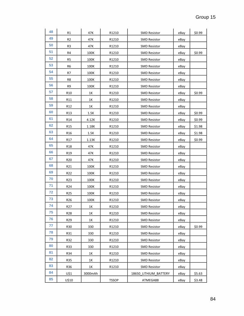
Group 15
84
48 R1 47K R1210 SMD Resistor eBay $0.99
49 R2 47K R1210 SMD Resistor eBay
50 R3 47K R1210 SMD Resistor eBay
51 R4 100K R1210 SMD Resistor eBay $0.99
52 R5 100K R1210 SMD Resistor eBay
53 R6 100K R1210 SMD Resistor eBay
54 R7 100K R1210 SMD Resistor eBay
55 R8 100K R1210 SMD Resistor eBay
56 R9 100K R1210 SMD Resistor eBay
57 R10 1K R1210 SMD Resistor eBay $0.99
58 R11 1K R1210 SMD Resistor eBay
59 R12 1K R1210 SMD Resistor eBay
60 R13 1.5K R1210 SMD Resistor eBay $0.99
61 R14 4.12K R1210 SMD Resistor eBay $0.99
62 R15 1.18K R1210 SMD Resistor eBay $1.98
63 R16 1.5K R1210 SMD Resistor eBay $1.98
64 R17 1.13K R1210 SMD Resistor eBay $0.99
65 R18 47K R1210 SMD Resistor eBay
66 R19 47K R1210 SMD Resistor eBay
67 R20 47K R1210 SMD Resistor eBay
68 R21 100K R1210 SMD Resistor eBay
69 R22 100K R1210 SMD Resistor eBay
70 R23 100K R1210 SMD Resistor eBay
71 R24 100K R1210 SMD Resistor eBay
72 R25 100K R1210 SMD Resistor eBay
73 R26 100K R1210 SMD Resistor eBay
74 R27 1K R1210 SMD Resistor eBay
75 R28 1K R1210 SMD Resistor eBay
76 R29 1K R1210 SMD Resistor eBay
77 R30 330 R1210 SMD Resistor eBay $0.99
78 R31 330 R1210 SMD Resistor eBay
79 R32 330 R1210 SMD Resistor eBay
80 R33 330 R1210 SMD Resistor eBay
81 R34 1K R1210 SMD Resistor eBay
82 R35 1K R1210 SMD Resistor eBay
83 R36 1K R1210 SMD Resistor eBay
84 U$1 3000mAh 18650_LITHIUM_BATTERY eBay $5.63
85 U$10 TSSOP ATMEGA88 eBay $3.48
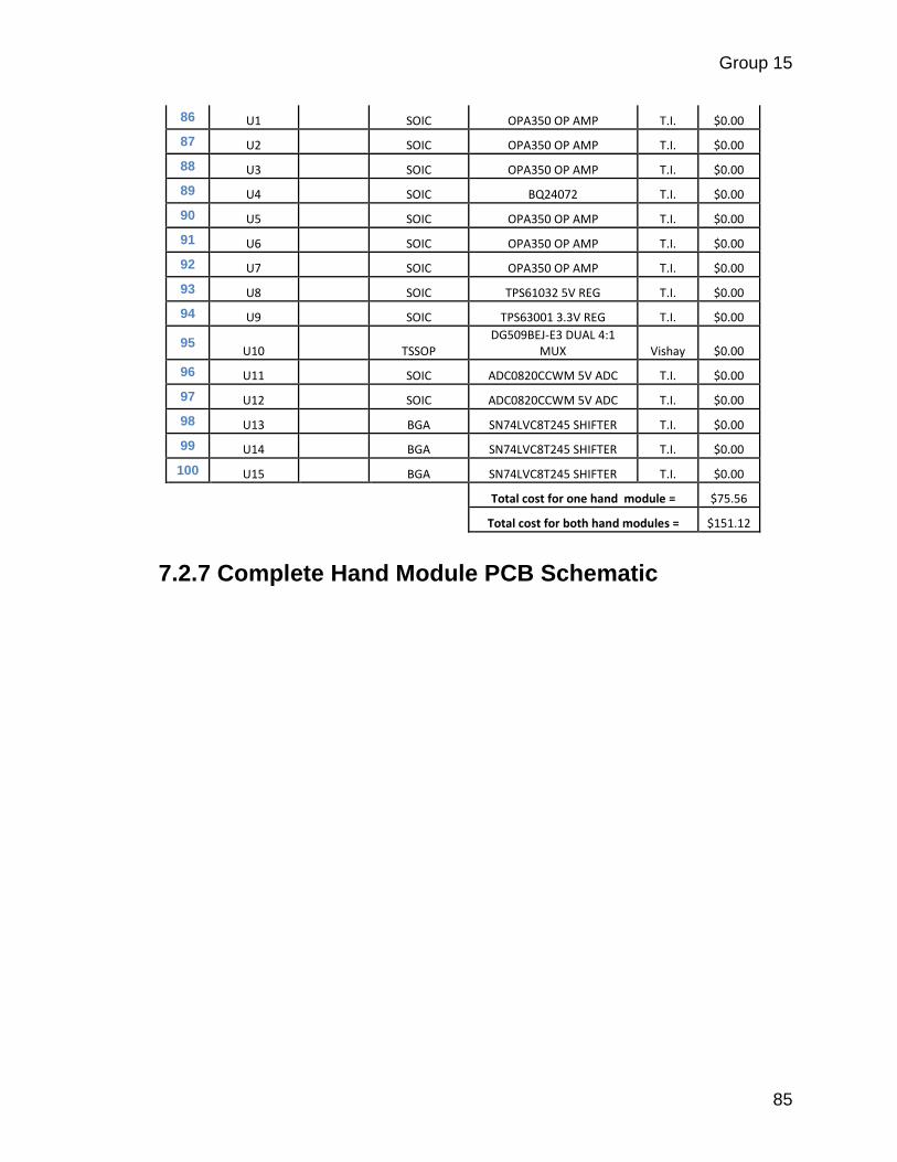
Group 15
85
86 U1 SOIC OPA350 OP AMP T.I. $0.00
87 U2 SOIC OPA350 OP AMP T.I. $0.00
88 U3 SOIC OPA350 OP AMP T.I. $0.00
89 U4 SOIC BQ24072 T.I. $0.00
90 U5 SOIC OPA350 OP AMP T.I. $0.00
91 U6 SOIC OPA350 OP AMP T.I. $0.00
92 U7 SOIC OPA350 OP AMP T.I. $0.00
93 U8 SOIC TPS61032 5V REG T.I. $0.00
94 U9 SOIC TPS63001 3.3V REG T.I. $0.00
95 U10 TSSOP
DG509BEJ-E3 DUAL 4:1 MUX Vishay $0.00
96 U11 SOIC ADC0820CCWM 5V ADC T.I. $0.00
97 U12 SOIC ADC0820CCWM 5V ADC T.I. $0.00
98 U13 BGA SN74LVC8T245 SHIFTER T.I. $0.00
99 U14 BGA SN74LVC8T245 SHIFTER T.I. $0.00
100 U15 BGA SN74LVC8T245 SHIFTER T.I. $0.00
Total cost for one hand module = $75.56
Total cost for both hand modules = $151.12
7.2.7 Complete Hand Module PCB Schematic
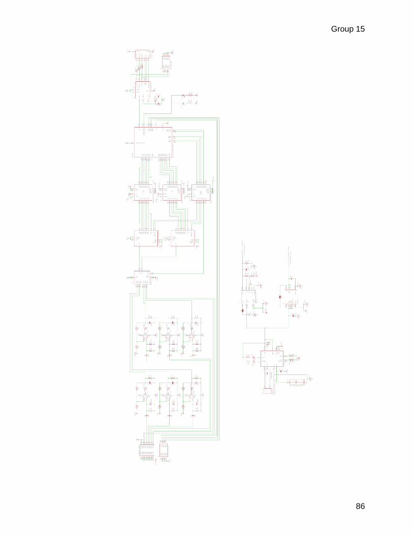
Group 15
86

Group 15
87
8.0 Assessing Latency and Jitter Latency is mentioned in many of sections above for good reason – no matter what Glove Drummer does accomplish, none of it will be of any worth if latency is is too great. A nominal value for the threshold of noticeable latency has been defined by the team at 15ms. Latency is refered to here as the time between the strike of the sensor to the time a sound is created. Some people may be able to recognize latency of less than 15ms while others might not be able to detect a latency of 30ms. Knowing that MCU’s have been extensively used in MIDI controllers, the team feels that latency should absolutely not be an issue with the use of an FPGA. However, the added devices which relay information between the FPGA of the hand modules and the Tiva C of the tabletop module will introduce additional latency. In addition to latency, jitter is another timing issue which is undesirable in musical instrument controllers. Jitter can be explained as individual drum strikes all having different latencies. Too much jitter can even sound worse than a uniform latency of greater than 15ms. The team plans to continue the design of Glove Drummer keeping the minimization of any latency or jitter of the utmost importance.
9.0 Administrative Content
9.1 Milestone Discussion During the Fall 2014 Senior Design I semester, the team focused mainly on defining what Glove Drummer should be. The divide and conquer method was used extensively in approaching the different aspects of designing the Glove Drummer system. Additionally the team used abstraction in order to focus on issues at an appropriate scale. Projected deadlines were made based on what the individual team members found through research. For example, since research had shown that the 9.5mm piezo disks had never been used in a glove controller, verifying their functionality was an initial concern. Therefore one of the first tasks the team completed was an in depth look at just how much analog conditioning circuitry was needed. In this case, the team decided only as much circuitry should be used as was required not to damage to ADC. Any remaining conditioning, or filtering, could easily be done within the FPGA. Planning the project so that no major road blocks were encountered proved a tricky task. It seemed that encountering more small obstacles that were easier to overcome was the only way to avoid being stumped by some major problem. The entire semester has been somewhat of a “sink or swim” situation. With each small problem the team solved, confidence was built that Glove Drummer would become a reality. After all an engineer’s main purpose is to solve problems. Sometimes solving a problem meant checking whatever math was involved so that some code ran correctly. Other times it meant removing unnecessary wiring or components from the breadboard to get rid of unwanted noise in the piezo signal. Many times

Group 15
88
wires were simply connected to the wrong pin. Identifying the real root of each problem is where the team felt real success. The team “learned to swim” with a little creativity, a lot of critical thinking, and the sheer determination not to sink. By the end of the Senior Design I semester, the team had already put together one functional hand model on a breadboard using the FPGA dev board, and ADC0820, and the FT232 UART/Serial converter. This was one the main goals: to get the MIDI controller (hand module) out of the way so that the MIDI sequencer (tabletop module) could be focused on in the Spring of 2015. Although one hand module had already been implemented on the breadboard, a custom PCB still needed to be mostly designed in the Fall semester. Having no errors in the PCB design may be the most critical aspect of completing this Senior Design project. Designing the schematic for the PCB was a gradual process in the search for a solution. The Simulated Annealing Algorithm was considered in the search for a PCB design solution. Early in the Fall semester many different solutions were explored, but as the end of the semester drew closer the team settled for the schematic shown in the PCB Planning section. Hardware design was a more pressing issue than software as the code can be altered throughout the Spring semester. Having said that, hardware and software design still went hand and hand through Senior Design I. In order to design plan the eventual PCB, some thought went into what software design would support the hardware design. Many decisions made by the team were nested inside one another and the absolute best solution was not always evident. Moving forward into the Senior Design II semester, the Glove Drummer team has confidence that with the experience gained through research and prototyping that the final realization of the system will be a success. Shown below is a timeline of the milestones the team set out to complete in Senior Design I & II.
Figure 65: Glove Drummer Milestone Timeline
9.2 Budget and Finance

Group 15
89
The financing of Glove Drummer began with some initial purchases made by Aaron. Experimenting with different parts and purchasing a few tools like wire strippers and breadboards meant that there would be some overhead costs. Some ICs that are not manufactured as DIP were found included in assembled PCBs. These circuit modules were very useful in prototyping, but also counted as overhead costs in designing Glove Drummer. Once the team learned to search for free samples from vendors, parts began to be selected based on sample availability. This not only reduced the total required cost but also allowed the team to experiment with a much wider selection of ICs. Ebay served as the source for many components because of its low prices on parts that could not be sampled. Going into Senior Design II, roughly $275 worth of parts, including the PCB, have yet to be purchased. It should also be noted that much of the remaining items to be purchased are duplicate items required for the second hand module. Table 6: The Glove Drummer Budget
Team Member Contribution
Aaron $400
Mike $150
Tim $150
Total Budget = $700
Table 7: Cost of Glove Drummer Subsystems
Parts Cost
Hand Module Components $180
Hand Module PCBs (4 layer) $150
Tabletop Module Parts $200
Parts not used in final design $170
Total cost of developing prototype = $700
10.0 Conclusions Throughout the course of Senior Design I the Glove Drummer team has sought to use the tools that have been given to us in our respective curriculums. Understanding how MIDI controllers and MIDI sequencers are designed has been a major advantage to the team. Also, using the divide and conquer method has helped the team to break a seemingly insurmountable workload into small manageable pieces. Division of labor amongst the team members helped to even
Group 15
90
further diminish the scope of the project. Tasks were broken down sometimes to the point where they were divorced from the needed solution in order to get the search for the solution jump started. This would lead to a snowball effect that eventually led to the final solution. This all sounds very abstract, and abstraction is in fact another technique the team used to focus in on a particular issue. For example, when writing a “Hello World” code in the C language, no consideration should be given to how to write that code strictly in machine language. The most important part of using these techniques is knowing how and when to use them. Of course having a strong mathematics and physics background is an even more basic and crucial skill to employ. Maybe the most basic and crucial skill is critical thinking. With all of these tools put together and a bit of creativity an engineer can accomplish almost anything. The initial shock at the scope of what was expected to be accomplished in Senior Design subsided more and more with each new problem the team overcame. Many new concepts such as SPI protocol, using ADCs/ DACs, wireless between MCUs, and files systems among other things. Not only would the tools mentioned above be needed but also careful organization and planning to make sure every task was finished correctly and on time. Being able to stay focused while moving from one task to the next required more abstraction from the tasks that were not being examined. Concentrating on areas of work that were yielding more results kept the teams morale up in between roadblocks. Also the time spent away from problem areas sometimes led to a fresh outlook and a more clever solution. Heading into Senior Design II, the team has many more obstacles to overcome and hopes to keep the momentum rolling during the transition from Senior Design I.
Appendix: References (source1). Retrieved October 24th, 2014, from
http://www.midi.org/aboutmidi/tut_history.php (source2). Retrieved November 2nd, 2014, from
http://www.drummagazine.com/features/print/200-greatest-drumming-moments-events
(source3). Retrieved November 15th, 2014, from https://www.princeton.edu/~achaney/tmve/wiki100k/docs/Persistence_of_vision.html
(source4). Retrieved November 20th, 2014, from http://headwize.com/?page_id=707
(source5). Retrieved October 23rd, 2014, from https://github.com/maniacbug/RF24
(source6). Retrieved November 12th, 2014, from http://www.voegler.eu/pub/audio/digital-audio-mixing-and-normalization.html

Group 15
91
(source7). Retrieved November 18th, 2014, from http://www.ti.com/lit/ds/symlink/adc0820-n.pdf
(source8). Retrieved November 3rd, 2014, from http://edrum.info/schematics.html (source9). Retrieved November 18th, 2014, from
http://avrprogrammers.com/articles/avr-spi-tips Palshikar, G. K. (n.d.). Simple Algorithms fro Peak Detection in Time-Series. Tata
Research Development and Design Center (TRDDC). Sholkman, F., Boss, J., & Wolf, M. (2012). An Efficient Algorith for Automatic
Peak Detection in Noisy Periodic and Quasi Periodic Signals. Algorithms, 588-603.