go forth with ttl
TRANSCRIPT

The Gigatron TTL Color Computer
Go Forth with TTL !
Forth for a Very Unusual Processor
Ken Boak
SV Fig. Forth Day 2019 .

In September of 1975, MOS Technology launched the 6502 at the Wescon75 Computer Conference in San Francisco.
25 year old, HP Engineer, Steve Wozniak, realised that this new microprocessor would be a game-changer and went on to incorporate it into the small computer he was developing.
That machine went on to become the Apple I.
Chuck Peddle and his team had created a very lean, stripped down, small die cpu.
Costing just $25, the 6502 was a fraction of the cost of its nearest competitor. At that time the Intel 8080 was $360 and the Motorola 6800 was $175 .
The 6502 was clearly a disruptive usurper.

16-bit TTL CPU board from Data General Nova 1200
In 1975 7400 TTL was the “Bread and Butter” of logic design:
.
7400 series TTL integrated circuits were developed in the early 1960’s. Initially quite expensive so mainly used in Military and Aerospace applications. By the early 1970’s TTL had become a versatile family of standardised, low
cost, easy to use logic. Typically about $1 per device. 7400 series logic was widely used in the design of minicomputers, including
the PDP-11, the Data General Nova 1200 and later models of PDP-8. TTL was a viable, faster and cheaper processing solution than the emerging
8-bit microprocessors such as MOS 6502, Intel 8080 and the Motorola 6800.
Essential Reading

The Gigatron TTL Computer – What is it?
Started as a Hackaday.io project in Spring 2017 by Marcel van Kervinck of The Hague, Netherlands.
Inspired by Apple I, Marcel wanted to show just what could be achieved without a microprocessor.
His personal challenge was to construct an 8-bit computer with integrated color video generation and sound based on simple, readily available, 74xx00 series TTL devices, plus ROM and RAM.
Gigatron uses a simple ALU design made from multiplexers and adders.
Avoids using the rare and obsolete 74181. Highly integrated cpu and video generation
hardware. ¼ VGA resolution: 160 x120 pixels, 64 colors Harvard design using 16-bit x 64K ROM Fewer than 40 ICs.
Marcel van Kervinck

Early Beginnings
The original was prototyped in about 1 month on a set of breadboards. 36 TTL chips handwired to form CPU with ROM and video RAM Designed from the outset to produce ¼ VGA color video and sound. Produced as an open source, educational, self build kit, now over 750 sold Inspired by the Apple I, but smaller, cheaper, more colorful and faster........
The Gigatron began life on a big breadboard.

The breadboard prototype shows the main functional blocks:

Then converted to a 2 layer pcb:

The Hardware Architecture Built as a Harvard machine with separate ROM and RAM
spaces - tailored to generate ¼ VGA video from RAM Clocked at 6.25MHz to meet VGA timing requirements Executes 1 instruction per clock cycle with simple pipeline
Consists of the following functional blocks:
ALU Arithmetic Logic Unit AC Accumulator PC Program Counter IR Instruction Register MAU Memory Address Unit CU Control Unit Registers X, Y, In, Out, Data

“A processor is like a nest of tangled pythons – all trying to eat each others’ tails.You have to carefully learn where to start unravelling it all from”

The Gigatron uses only 36 simple TTL devices to implement its Harvard architecture - in fewer than 1000 gates!
Dual 4:1 Multiplexers 74xx153 4 bit full adders 74xx283 4-bit counters 74xx161 Octal Latches 74xx377 Various basic gates including OR, AND, Inverters Serial to parallel shift register for keyboard entry 74HC595 Plus 32K x 8 SRAM and 64K x 16 bit EPROM With the exception of the EPROM and RAM – all of these parts
were available in standard 7400 series TTL back in 1975
Average price per 7400 series IC was about $1 each in 1975.
RAM was still very expensive in 1975. 4K bytes implemented as 32 x Intel 2102 SRAMs would cost at least $96. (Byte Magazine October 1975).

The Gigatron PCB – with main functional blocks highlighted

The Instruction Set 8-bit wide instruction word providing 8 opcodes, 8 addressing modes
and 4 data sources for operands.
8 x 8 x 4 = 256 instruction combinations The Accumulator AC always provides one operand for the ALU
Memory load/store LD, ST
Arithmetic ADD, SUB
Logical AND, OR, XOR
Unconditional jumps JMP, BRA
Conditional jumps BGT, BGE, BLT, BLE, BEQ, BNE
Others NOP, CTRL

Instruction Decoding
|---Operation---|-----Mode-----|----Bus---|
0 LOAD [D],AC D1 AND [X],AC RAM2 OR [Y,D],AC AC3 XOR [Y,X],AC IN4 ADD [D],X5 SUB [D],Y6 STORE [D],OUT7 JUMP [Y,X++],OUT
I7 I6 I5 I4 I3 I2 I1 I0


The Instruction Decoder uses a “Diode ROM” driven from a 74HC138 decoder to feed the correct instruction pattern to the ALU.

ALU - Arithmetic Logic Unit
The ALU forms the functional core of the Gigatron processor. Provides 8-bit ADD, SUB arithmetic operations, plus AND, OR and
XOR bitwise logical operations It’s an extendible bitslice design. Constructed from 10 ICs: 8 x 74HC153 multiplexers and 2 x 74HC283 4-bit adders.
Provides a readily available alternative to the now obsolete and rare 74181 4-bit ALU
ALU is equivalent to approximately 200 logic gates.
Based on an original design by TTL CPU builder Dieter Muller.

The ALU is based on the 74xx153 dual 4:1 Multiplexer
The 4:1 multiplexer can be used to generate any logic function Q of its two inputs A and B just by wiring various logic levels, 0 or 1 to the inputs I0 to I3.
Applying a different 4-bit pattern to I0:I3 you can create AND, OR, XOR, invert or any other of 16 common logic functions of A and B. It’s a programmable function generator!
As a 4:1 multiplexer:
Normally you would use the A and B inputs to select which one of the inputs I0 to I3 that you wish to appear at the output Q.
However there is a neat trick, and an altogether more ingenious way of using the basic multiplexer that lends itself perfectly to constructing an ALU:
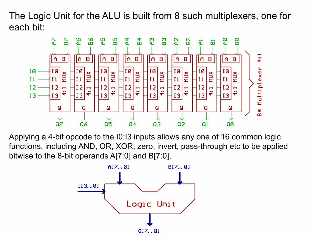
The Logic Unit for the ALU is built from 8 such multiplexers, one for each bit:
Applying a 4-bit opcode to the I0:I3 inputs allows any one of 16 common logic functions, including AND, OR, XOR, zero, invert, pass-through etc to be applied bitwise to the 8-bit operands A[7:0] and B[7:0].

The Arithmetic section is made from two 4-bit adders and two of the 74xx153 logic units.
As the 74xx153 are dual 4:1 multiplexers you conveniently get both logic units from the same 8 ICs!
The two 74xx283 4-bit adders provides 8-bit addition and subtraction.
An optional 7xx157 mux may be used if Right Shift operation is required. On the Gigatron, right shifts are performed using a look up table in ROM

RAM, X and Y Registers and Video Generation Hardware
• From the outset, the Gigatron was designed to output a 64 color image to a VGA display using highly integrated hardware.
• The resolution is 160 by 120 pixels - effectively ¼ VGA
• The X and Y registers address a 32K RAM – and effectively hold the horizontal and vertical location of the pixel.
• The X register is an 8-bit counter which can auto-increment to select the next pixel in the line of video.
• The video RAM holds the RGB video (2 bits of each) and the remaining 2 bits are for the horizontal and vertical sync signals.
• The VGA video signal is created using a simple resistor network DAC.• • The audio signal uses a 4-bit resistor ladder network with waveform tables
stored in ROM

The audio and video generation is also kept very simple:

vCPU – A 16-bit virtual machine• • Gigatron achieves flexibility and easier programming by implementing
a 16-bit von Neumann virtual machine on top of the 8-bit Harvard architecture. vCPU uses 37 instructions expressed as bytecodes.
• • The vCPU interpreter is written in native 8-bit machine language,
executing code from the ROM.The instruction bytecodes are merely offsets from a base address into the ROM. The 16-bit vCPU executes its code from RAM.
• vCPU executes 16-bit operations which are precisely timed to fit in with the video blanking. Instructions are 2.25uS to 4.5uS duration.
• Programming Model: vCPU implements the following registers•
vAC ACcumulator (16-bits) vPC Program Counter vLR Link Register (16-bits) vSP Stack Pointer (8-bits)

Mnem. Encoding #C Description----- --------- -- -----------ST $5E DD 16 Store byte in zero page ([D]=vAC&256)STW $2B DD 20 Store word in zero page ([D],[D+1]=vAC&255,vAC>>8)STLW $EC DD 26 Store word in stack frame ([vSP+D],[vSP+D+1]=vAC&255,vAC>>8)LD $1A DD 18 Load byte from zero page (vAC=[D])LDI $59 DD 16 Load immediate small positive constant (vAC=D)LDWI $11 LL HH 20 Load immediate word constant (vAC=$HHLL)LDW $21 DD 20 Word load from zero page (vAC=[D]+256*[D+1])LDLW $EE DD 26 Load word from stack frame (vAC=[vSP+D]+256*[vSP+D+1])ADDW $99 DD 28 Word addition with zero page (vAC+=[D]+256*[D+1])SUBW $B8 DD 28 Word subtraction with zero page (vAC-=[D]+256*[D+1])ADDI $E3 DD 28 Add small positive constant (vAC+=D)SUBI $E6 DD 28 Subtract small positive constant (vAC-=D)LSLW $E9 28 Shift left ('ADDW vAC' will not work!) (vAC<<=1)INC $93 DD 16 Increment zero page byte ([D]++)ANDI $82 DD 16 Logical-AND with small constant (vAC&=D)ANDW $F8 DD 28 Word logical-AND with zero page (vAC&=[D]+256*[D+1])ORI $88 DD 14 Logical-OR with small constant (vAC|=D)ORW $FA DD 28 Word logical-OR with zero page (vAC|=[D]+256*[D+1])XORI $8C DD 14 Logical-XOR with small constant (vAC^=D)XORW $FC DD 26 Word logical-XOR with zero page (vAC^=[D]+256*[D+1])PEEK $AD 26 Read byte from memory (vAC=[vAC])DEEK $F6 28 Read word from memory (vAC=[vAC]+256*[vAC+1])POKE $F0 DD 28 Write byte in memory([[D+1],[D]]=vAC&255)DOKE $F3 DD 28 Write word in memory([[D+1],[D]],[[D+1],[D+1]=vAC&255,vAC>>8)LUP $7F DD 26 ROM lookup, needs trampoline in target page (vAC=ROM[vAC+D])BRA $90 DD 14 Branch unconditionally (vPC=(vPC&0xff00)+D)BCC $35 CC DD 28 Test vAC and branch conditionally.
CC can be EQ=$3F, NE=$72, LT=$50, GT=$4D, LE=$56, GE=$53
vCPU Instruction Set

Forth Thoughts?
vCPU is a flexible, 16-bit virtual cpu which can be used to host the Forth primitives. Stack structures are implemented in RAM using ALLOC to modify the stack pointer, LDLW
and STLW to load and store the top of stack. vSP is then the data stack pointer. We can use ALLOC, LDLW, STLW on it. Zero page variables: IP, RSP, W, Next, DoColon IP = Instruction Pointer RSP = Return Stack Pointer W = Work Register NEXT vCPU function to dispatch the next threaded instruction

Further primitives may then be added:PLUS
DUP
DoCOLON vCPU function to enter threaded code

A start has been made on a Forth implementation running on the vCPU:
This is however very much a work in progress and we are looking for fellow enthusiasts to help with the implementation.

The Gigatron Ecosystem Gigatron is a constantly evolving project with an active community and many
new developments since the original machine. For code development, there is an online emulator, an assembler and other
tools written in Python. Gigatron comes with a TinyBASIC in ROM and a hex monitor program inspired
by WozMon – originally written for the Apple 1 by Steve Wozniak “Pluggy McPlugface” – an adaptor that allows a PS/2 keyboard to be used A C compiler based on lcc – write standard code using modern tools. v6502 allows the Gigatron to emulate the 6502 – with video - at about
0.125MHz - but gives access to a wealth of software such as Microchess, figForth and MS floating point BASIC.
A RAM and port expansion board that allows use of SPI hardware such as SD
cards, port expanders and FRAM non-volatile memory. By using 74F series logic, Gigatron can be overclocked to 12.5MHz – twice the
standard clock frequency.

V6502 emulates a 6502 and allows existing 6502 applications to be run:

TinyBASIC

WozMon – in 254 words of vCPU!

An emulator with screen memory, CPU & vCPU:
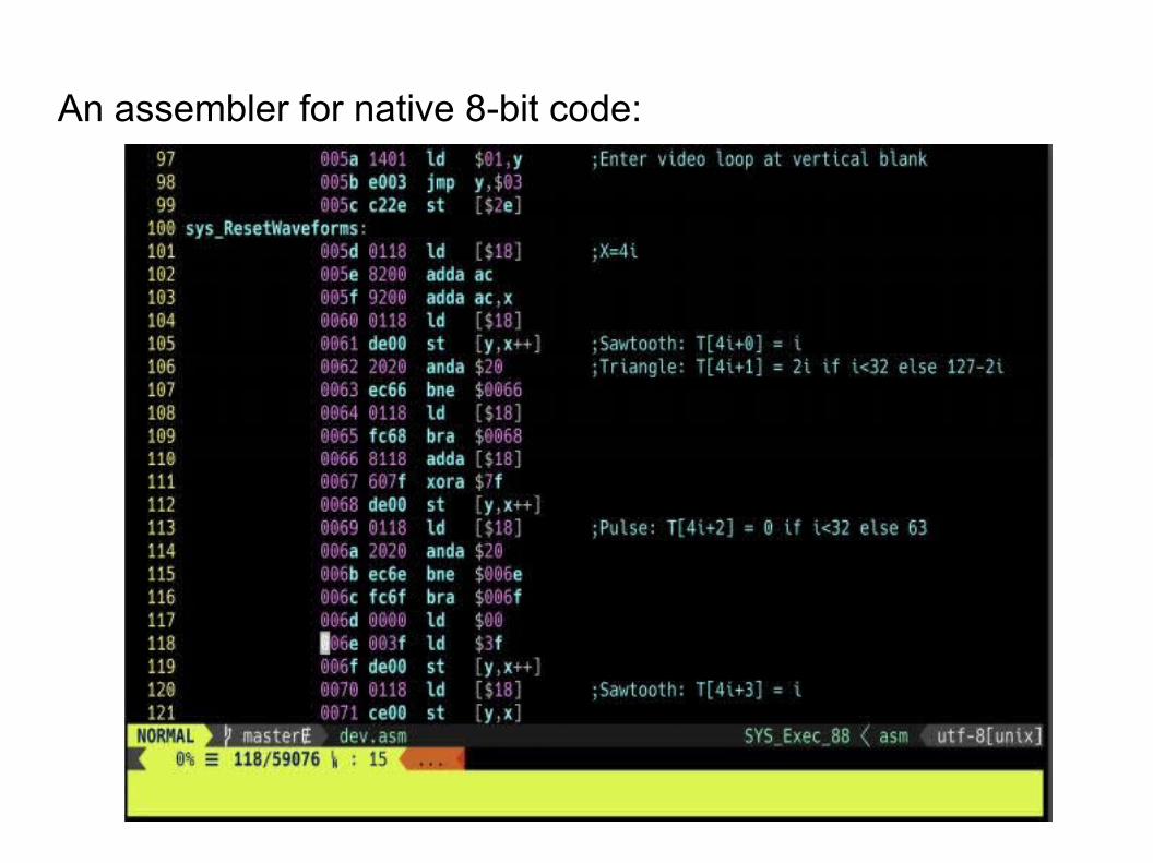
An assembler for native 8-bit code: