grand challenges in oxides...
TRANSCRIPT

Grand Challenges in Oxides Research
Nicola Spaldin
Materials Department
UC Santa Barbara
805 893-7920
with valuable input from:Leon Balents (UCSB), Jeroen van den Brink (U Leiden), Jaques Chakalian (U Arkansas),
Matthew Fisher (UCSB), Michael Fisher (U Maryland), Supratik Guha (IBM), Werner Hanke
(U Wurzburg), Daniel Khomskii (U Koln), R. Ramesh (UC Berkeley), Art Ramirez (Bell
Labs.), Richard Scalettar (UC Davis), Darrell Schlom (Penn State), Jim Speck (UCSB),
Susanne Stemmer (UCSB), Chris van de Walle (UCSB)
the CMMP 2010 and BESAC Grand Challenges reports

The simplest complex oxide: SrTiO3
without
oxygen
vacancies
with
oxygen
vacancies
Semiconductor physics: The value ofseeing nothing, J. Mannhart and D. G.Schlom, Nature 430, 620 (2004)
Atomic-scale imaging of nano-engineered oxygen vacancy profiles inSrTiO3, D. Muller et al., Nature 430,657 (2004)

Grand challenge
To achieve the same level of synthetic control and fundamental
understanding as is currently attained in semiconductors and
simple metals

http://pubs.usgs.gov/fs/2002/fs087-02/
Why oxides?
abundance!
non-toxic
polarizability just right
nitrides too covalent
fluorides too ionic
diverse chemistries, structures and dimensionalities
strong correlations! behavior of one electron explicitly influences the others

Strong correlations
Spin/orbital/lattice couplings have similar energy scales
small energy changes (surfaces, interfaces, defects, external perturbations) can
shift balance between competing large energy interactions and vastly alter ground
state
TUNABILITY!
a wide range of couplings:electron-lattice
electron-spin(-lattice)
spin-orbital
potential technological relevance:high-k dielectricsferroelectricityhigh-Tc superconductivitylarge thermopower
multiferroismmagnetoelectricitymagnetoresistance
spintronics
piezomagnetismmagnetic frustration

Strong correlations
Spin/orbital/lattice couplings with similar energy scales
small energy changes (surfaces, interfaces, defects, external perturbations) can
shift balance between competing large energy interactions and vastly alter ground
state
TUNABILITY!
Complexity in strongly correlated electronic systems, E. Dagotto, Science 309, 257 (2005)

Comparison with conventional semiconductors
Conventional semiconductors
Physics:
— large overlap of s/p orbitals gives
extended wavefunctions
— no intrinsic magnetism or other
correlations
Technology:
— Quality: high! can be fabricated into
complex structures
— Understanding: Semiconductor
modeling is straightforward
— Tunability: control charge with modest
doping/ E fields
Complex oxides
Physics:
— localization of 3d/2p orbitals gives
strong Coulomb interactions
— diverse magnetic and other strong
correlations
Technology:
— Quality: materials chemistry
challenging; fabrication less developed
— Understanding: strong correlations
challenging to theoretical tools
— Tunability: high! due to competing
ordered states

Comparison with conventional semiconductors
Conventional semiconductors
Physics:
— large overlap of s/p orbitals gives
extended wavefunctions
— no intrinsic magnetism or other
correlations
Technology:
— Quality: high! can be fabricated into
complex structures
— Understanding: Semiconductor
modeling is straightforward
— Tunability: control charge with modest
doping/ E fields
Complex oxides
Physics:
— localization of 3d/2p orbitals gives
strong Coulomb interactions
— diverse magnetic and other
correlations
Technology:
— Quality: materials chemistry
challenging; fabrication less developed
— Understanding: strong correlations
challenging to theoretical tools
— Tunability: high! due to competing
ordered states
To achieve the same level of synthetic control and fundamental
understanding as is currently attained in semiconductors and simple metals
vastly richer physics suggests entirely new functionalities
provided Oxides Grand Challenge can be met:

Why now?
Quantum Hall Effect at ZnO/(Zn,Mg)O interface high quality samples
A. Tsukazaki et al. Quantum Hall Effect in Polar
Oxide Heterostructures, Science 315, 1388 (2007)
Understanding:
improved experimental probes (ARPES, STM, SNS)
theory/computation able to address intricacies
numerically
Growth/synthesis:

Business Partner Transformation
© 2006 IBM CorporationIBM Confidential © Copyright IBM Corporation 2006
IBM Research
© 2004 IBM CorporationSupratik Guha
Fully processed transistorwith high-k/metal gate:
Silicon
High-K
Metal Gate
Silicon
High-K
Metal Gate
Existing technology need: High-k oxide-based CMOS technology:
This is the first major technology application
for nanoscale metal oxides in electronics
IBM high-k product : Expected 20080.010.11
0.001
0.01
0.1
1
10
100
1000
1994 2006
Active Power
Passive Power
Gate Length (microns)
Po
wer
Den
sit
y (
W/c
m2
)
Gate Length (microns)
Gate Leakage Power
0.010.11
0.001
0.01
0.1
1
10
100
1000
1994 2006
0.010.11 0.010.11
0.001
0.01
0.1
1
10
100
1000
0.001
0.01
0.1
1
10
100
1000
1994 2006
Active Power
Passive Power
Gate Length (microns)
Po
wer
Den
sit
y (
W/c
m2
)
Gate Length (microns)
Gate Leakage Power
Gate leakage power growing
exponentially as gate length is reduced
C = k/d; Need a high-k replacement for
SiO2 to continue CMOS scaling

Outline
Sub-challenges:
growth/synthesis
theory/computation
Two most exciting current/developing areas:
oxide-oxide interfaces
multi-functional oxides
A “mini seminar” on theory/experiment interplay in multiferroics
To achieve the same level of synthetic control and fundamental
understanding as is currently attained in semiconductors and simple metals

Challenge: Synthesis
2 c
m
BiFeO3
grown from B2O3/Bi2O3/Fe2O3 flux
Bi2Fe4O9 more stable
Fe3O4 decomposition product!

Single crystal growth
need for bulk single crystal growth
best (sometimes essential) for accurate characterization (dielectric
measurements, neutrons, x-rays)
required as substrates for homoepitaxy
new materials: ternaries and quaternaries
dedicated equipment and operators
many oxides melt at high temperatures (> 1500oC)
some require toxic fluxes (e.g. Bi)
some require high pressure (many Bi-based multiferroics)
cubic anvil press
at Kyoto University
typical operation:
6GPa and 1000oC
New materials synthesis and crystal growth study
Paul Peercy and Art Ramirez, tomorrow am

Thin film growth
Films offer additional capabilities
stabilizing phases which are not the bulk thermodynamic ground state
chemical control through layer-by-layer deposition
multilayers with precisely engineered interfaces
modifying properties with strain
required for devices
Need for improved film quality
complex oxide films are often farfrom stoichiometry
current composition control limitsaround 1%
oxide MBE (molecular beam epitaxy)versus PLD (pulsed laser deposition)
3.85
3.90
3.95
4.00
4.05
4.10
0.6 0.8 1.0 1.2 1.4 1.6
c-ax
is L
atti
ce C
onst
ant
(Å)
Sr Content
Homoepitaxial SrTiO3 / SrTiO
3
SrTiO3 substrate
3.905 Å
MBE Brooks et al.
PLD Ohnishi et al.
PLD Suzuki et al.
Sputtering Fuchs et al.
Sr/Ti Ratio

Challenges in theoreticaldescription of complex oxides
strong correlations lead to many-body effects
traditionally (successfully) described with model Hamiltonians
complete description of structure and chemistry essential
traditionally (successfully) performed within a mean-field treatment
need techniques that include chemistry, structure and many-
body interactions on an equal footing
Steven White
tomorrow am

Incorporating many-body effects in“structure and chemistry” methods
interacting many-electron system
Kohn-Sham Equations
system of non-interacting electrons
{T+Vei(r)+VH(r)+Vxc(r)} i(r) = i i(r)
Allows us in principle to calculate ground state
properties:
charge densities and energies, crystal structures, electronic band
structures, magnetic ordering, phonon frequencies, ferroelectric
polarizations, dielectric response, piezoelectric coefficients…
Density Functional Theory

Incorporating many-body effects in“structure and chemistry” methods
BUT…
Vxc(r ) is approximated
“Standard” local density approximation (LDA) treats as a homogeneous
electron gas
Beyond-LDA methods:
LDA+U attempts to incorporate Coulomb repulsions (U)
Self-interaction corrections (SIC) attempt to account for spurious self-XC
LDA+DMFT (dynamical mean field theory)
Downfolding:
Extract essential interaction parameters from LDA and construct a model
Needs:
Greater supercomputing capacity in central facilities
A system for supporting the maintenance of public codes
{T+Vei(r)+VH(r)+ Vxc(r) } i(r) = i i(r)

Other challenges in DFT-based theory:Finite Electric Fields
Two difficulties:
1) Infinite crystal in uniform external
field does not have a ground state:
2) Potential with electric field is non-
periodic
e-
I. Souza, J. Iniguez and D. Vanderbilt, First-principles approach to
insulators in finite electric fields, Phys. Rev. Lett. 89, 117602 (2002)
M. Stengel and N.A. Spaldin, Ab-initio theory of metal-insulator interfaces
in finite electric field, PRB 75, 205121 (2007).
Solved (very recently) using tricks:

Outline
Sub-challenges:
growth/synthesis
theory/computation
Two most exciting current/developing areas:
oxide-oxide interfaces
multi-functional oxides
A “mini seminar” on theory/experiment interplay in multiferroics

Oxide-oxide interfaces
Band Gap
“The interface is the device”
Herbert Kroemer,
Nobel lecture, Dec 8 2000

Oxide-oxide interfaces
Band Gap
“The interface is the device”
Herbert Kroemer,
Nobel lecture, Dec 8 2000
Functional
Oxide
I
Functional
Oxide
II
?!

Example of new functionality atoxide-oxide interfaces
Artificial charge modulation in
atomic scale perovskite
titantate superlattices, A.
Ohtomo et al., Nature 419, 378
(2002)
Electron microscopy image
of LaTiO3 layers (bright)
spaced by SrTiO3 layers

Example of new functionality atoxide-oxide interfaces
Artificial charge modulation in
atomic scale perovskite
titantate superlattices, A.
Ohtomo et al., Nature 419, 378
(2002)
Electron microscopy image
of LaTiO3 layers (bright)
spaced by SrTiO3 layers
SrO
LaO
TiO2 (Ti??)
LaTiO3
Ti3+ (3d)1
Mott insulator
SrTiO3
Ti4+ (3d)0
Band insulatorTiO2 (Ti4+) (3d0)
TiO2 (Ti3+) (3d1)
SrO
LaO
The conflicted d electron spreads out…
(magnetic) metal at the interface!

Incompatible magnetism atoxide-oxide interfaces
“A-type” antiferromagnet
e.g. LaMnO3
“G-type” antiferromagnet
e.g. LaFeO3
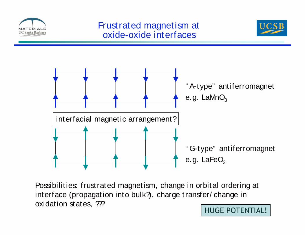
Frustrated magnetism atoxide-oxide interfaces
“A-type” antiferromagnet
e.g. LaMnO3
“G-type” antiferromagnet
e.g. LaFeO3
interfacial magnetic arrangement?
Possibilities: frustrated magnetism, change in orbital ordering at
interface (propagation into bulk?), charge transfer/change in
oxidation states, ??? HUGE POTENTIAL!

Summary
Tremendous progress in synthesis, characterization and
understanding of novel complex oxides
Many new (unanticipated) physical phenomena emerging in single
phases and at interfaces
Demand for oxides in existing technological applications
high-k dielectrics
oxides as semiconductors
dissipationless wires from high (room) temperature superconductors
Possibility for entirely new device paradigms
strong correlations
multifunctionality E field or photon
or stress or H field
giant optical
or electric or
magnetic or
mechanical
response
INPUT
OUTPUT
integrated
complex
functional
oxide
Plan for coordinating fundamental discoveries with new technologies?