graphene compared to noble metals
DESCRIPTION
Paper comparing graphene and noble metals contact resistanceTRANSCRIPT

Graphene plasmonic lens formanipulating energy flowGuoxi Wang, Xueming Liu, Hua Lu & Chao Zeng
State Key Laboratory of Transient Optics and Photonics, Xi’an Institute of Optics and Precision Mechanics, Chinese Academy ofSciences, Xi’an 710119, China.
Manipulating the energy flow of light is at the heart of modern information and communicationtechnologies. Because photons are uncharged, it is still difficult to effectively control them by electricalmeans. Here, we propose a graphene plasmonic (GP) lens to efficiently manipulate energy flow byelaborately designing the thickness of the dielectric spacer beneath the graphene sheet. Different fromtraditional metal-based lenses, the proposed graphene plasmonic lens possesses the advantages of tunabilityand excellent confinement of surface plasmons. It is found that the proposed lens can be utilized to focus andcollimate the GP waves propagating along the graphene sheet. Particularly, the lens is dispersionless over awide frequency range and the performance of lens can be flexibly tuned by adjusting the bias voltage. As anapplication of such a lens, the image transfer of two point sources with a separation of l0/30 is demonstrated.
Surface plasmon polaritons (SPPs) are electromagnetic surface waves resulting from the coupling of theelectromagnetic field to the collective plasma excitations of metal1. Due to the ability to overcome thediffraction limit of light in microchip-sized devices, SPPs are considered as one of the most promising
candidates for nanophotonic components2,3. In recent years, varieties of plasmonic devices with special function-alities are proposed and investigated4–8. In these researches, the noble metals, such as silver and gold, have beenpopular materials to support SPP waves in the infrared and visible regimes. However, the noble metals possessenormous loss in the frequency regimes of interest. Especially, it is difficult to vary the permittivity functions ofthe noble metals9,10. These insurmountable obstacles severely limit the propagation length of SPP waves and thetunability of the metallic plasmonic devices.
Graphene, which is a single sheet of carbon atoms in a hexagonal lattice, has drawn much attention for itsexceptional electrical and optical properties11. The complex conductivity (sg 5 sg,r 1 isg,i) of graphene is deter-mined by Kubo’s formula, which expresses the dependence on the radian frequency v, charged particle scatteringrate C, temperature T, and chemical potential mc
12,13. Comparing with noble metals, the most advantage ofgraphene for plasmonic applications is the capability to tune surface conductivity by gate voltage, electric field,magnetic field, and/or chemical doping14. In addition, the effective mode index for the TM-polarized GP wavesalong the graphene sheet can reach to ,100 in the mid-infrared regime15. As a result, the GP waves can be tightlyconfined to the graphene sheet, with effective wavelength (lGP) much smaller than free space wavelength (l0).Meanwhile, the imaginary part of the wavenumber is relatively small, which means that the damping loss of GPwaves is relatively low and the propagation length could be dozens of lGP
16. Due to the above advantages,graphene has been proved to be a suitable alternative material to noble metals. Recently, a lot of GP devices havebeen proposed and investigated17–25. For example, Engheta et al. reported that by designing and manipulatingspatially inhomogeneous conductivity patterns across a flake of graphene, one can treat graphene as a one-atom-thick platform for infrared metamaterials15. The inhomogeneous conductivity can be obtained by applyingdifferent gate voltages or by designing the thickness of dielectric spacer underneath the graphene sheet. Wanget al. studied the optical coupling of GPs between graphene sheets. They employed the coupling of GPs to designthe optical splitters, spatial switches, and Mach-Zehnder interferometers16. Perruisseau-Carrier et al. proposed aterahertz plasmonic antenna by using a graphene stack. The GP antenna possesses the advantages of high inputimpedance and easy fabrication26. All these works have proved that graphene possesses excellent confinement ofSPPs and high tunability, which makes it an ideal material to realize various plasmonic devices working from theterahertz to the visible regimes17.
The ability to manipulate optical fields and the energy flow of light is at the heart of modern information andcommunication technologies, as well as quantum information processing schemes27. However, because photonsare uncharged, it is still elusive to effectively control them by electrical means27. In recent years, many metal-basedplasmonic devices for subwavelength light management have been proposed theoretically and demonstrated
OPEN
SUBJECT AREAS:NANOPHOTONICS AND
PLASMONICS
OPTICAL MATERIALS ANDSTRUCTURES
Received6 November 2013
Accepted27 January 2014
Published12 February 2014
Correspondence andrequests for materials
should be addressed toX.M.L. ([email protected].
cn)
SCIENTIFIC REPORTS | 4 : 4073 | DOI: 10.1038/srep04073 1
experimentally28–30. For example, Liu et al. numerically demonstratedthe efficiently manipulating SPPs based on transformation optics invisible regime28. They showed that the propagation of SPPs could beflexibly controlled by carefully tuning the dielectric material prop-erties adjacent to a metal. Zentgraf et al. experimentally demon-strated plasmonic Luneburg lens and Eaton lens by tailoring thetopology of a dielectric layer adjacent to the metal surface29. Theyproved that the optical properties in these lenses are changed gradu-ally and thus the scattering could be significantly reduced. Differentfrom the above metal-based plasmonic lenses, we propose a gra-phene-based self-focus (Selfoc) lens for manipulating the energy flowof GP waves in infrared (IR) regime. By applying external gate volt-age, the proposed Selfoc lens can be used to focus and collimate GPwaves that propagate along the graphene. In addition, we investigatethe dispersion of the proposed Selfoc lens. It is found that such a lensis dispersionless over a wide frequency range. Finally, to illustrate theapplication of the proposed lens, we demonstrate that the imagetransfer of two point sources separated by a distance of l0/30 (l0 isthe incident wavelength in vacuum) can be realized on the graphene.The proposed graphene-based Selfoc lens can be flexibly tuned bycontrolling the external bias voltage and possesses high confinement
of SPPs, which paves the way for effectively manipulating energy flowof light at nanoscale.
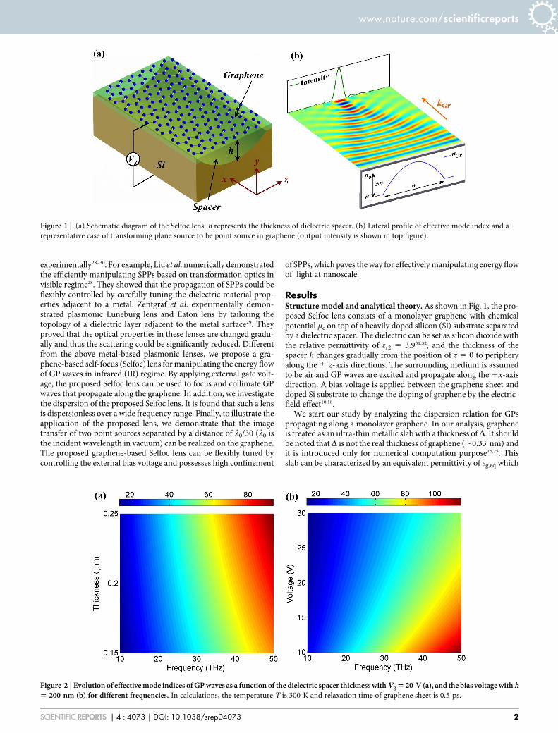
ResultsStructure model and analytical theory. As shown in Fig. 1, the pro-posed Selfoc lens consists of a monolayer graphene with chemicalpotential mc on top of a heavily doped silicon (Si) substrate separatedby a dielectric spacer. The dielectric can be set as silicon dioxide withthe relative permittivity of er2 5 3.931,32, and the thickness of thespacer h changes gradually from the position of z 5 0 to peripheryalong the 6 z-axis directions. The surrounding medium is assumedto be air and GP waves are excited and propagate along the 1x-axisdirection. A bias voltage is applied between the graphene sheet anddoped Si substrate to change the doping of graphene by the electric-field effect10,18.
We start our study by analyzing the dispersion relation for GPspropagating along a monolayer graphene. In our analysis, grapheneis treated as an ultra-thin metallic slab with a thickness ofD. It shouldbe noted that D is not the real thickness of graphene (,0.33 nm) andit is introduced only for numerical computation purpose16,25. Thisslab can be characterized by an equivalent permittivity of eg,eq which
Figure 1 | (a) Schematic diagram of the Selfoc lens. h represents the thickness of dielectric spacer. (b) Lateral profile of effective mode index and a
representative case of transforming plane source to be point source in graphene (output intensity is shown in top figure).
Figure 2 | Evolution of effective mode indices of GP waves as a function of the dielectric spacer thickness with Vg 5 20 V (a), and the bias voltage with h5 200 nm (b) for different frequencies. In calculations, the temperature T is 300 K and relaxation time of graphene sheet is 0.5 ps.
www.nature.com/scientificreports
SCIENTIFIC REPORTS | 4 : 4073 | DOI: 10.1038/srep04073 2

is given by16
eg,eq~1zisgg0=(k0D), ð1Þ
where sg represents the conductivity of graphene, g0 < 377 V is theimpedance of air, and k0 5 2p/l0 is the wavenumber in vacuum.With Maxwell’s equation, the dispersion of TM-polarized guidedwaves in graphene can be expressed as14
er1ffiffiffiffiffiffiffiffiffiffiffiffiffiffiffiffiffiffiffiffiffiffiffiffiffiffiffiffiffiffiffiffik2
GP{ er1v2=c2ð Þp z
er2ffiffiffiffiffiffiffiffiffiffiffiffiffiffiffiffiffiffiffiffiffiffiffiffiffiffiffiffiffiffiffiffik2
GP{ er2v2=c2ð Þp z
isg
ve0~0, ð2Þ
where kGP is the wavenumber of the guided modes, er1 and er2 are thedielectric permittivities of air and spacer, respectively.
Within the random-phase approximation, the dynamic optical res-ponse of graphene can be derived from the Kubo’s formula consisting
of the interband and intraband contributions: sg 5 sinter 1 sintra33. In
the THz and infrared ranges, the intraband transition of electronsdominates. On condition that mc ? kBT, where kB is theBoltzmann’s constant, the surface conductivity of graphene can besimplified to a Drude-like form25,34
sg~ie2mc
p�h2 vzit{1ð Þ, ð3Þ
here t is the momentum relaxation time, e and �h are the electroncharge and reduced Planck’s constant, respectively. The carrier relaxa-tion time t determined by the carrier mobility m in graphene as t 5
mmc/(eVf2)35. Recently, it has been reported that the carrier mobility of
m 5 8000 cm2/(V?s) of graphene can be obtained by mechanicalcleavage of bulk graphite and then transferred to SiO2/Si substrate36,and m 5 230000 cm2/(V?s) can be experimentally achieved in high-quality suspended graphene37. When the chemical potential mc is0.15 eV with a certain gate voltage38, the above carrier motilities corre-spond to the relaxation times of t 5 0.12 ps and t 5 3.45 ps, respect-ively. Here, we choose t 5 0.5 ps. This value follows the ballistictransport features of graphene, whose mean free path was measuredto be up to 500 nm at room temperature16. It should be noted that thecarrier relaxation time t can affect the imaginary part of the effectivemode index of the graphene, which may result in the distortion ofimages and the deteriorated focusing effect. In practice, therefore, thecarrier mobility and relaxation time should be appropriately tuned toreduce the distortion of images and the deteriorated focusing effect. Inour analysis, mc~�hVf
ffiffiffiffiffiffiffipnsp
, where Vf 5 106 m/s is the Fermi velocityand ns is the sheet doping of graphene32. In the proposed Selfoc lens, ns
can be controlled using an external bias voltage following
CoxVg~ens, ð4Þ
where Cox 5 er2e0/h is the gate capacitance, and Vg is the external biasvoltage32. Based on the above equations, the effective mode indices nGP
(5kGP/k0) of GP waves for different thicknesses of dielectric spacerand bias voltages can be obtained. As shown in Fig. 2, it is found thatnGP can be adjusted by tuning the h and Vg. In the following discus-sions, we mainly employ the changing of h to control the effectivemode index nGP and manipulate the propagation of GP waves in
Figure 3 | Lateral profile of the effective mode index nGP (green line) andthe thickness of the dielectric spacer h (blue line). In calculations,
the bias voltage is 20 V and the incident frequency is 40 THz.
Figure 4 | Simulation results of the Selfoc lens, showing the amplitude of the y component of electric field (Ey) of GP waves. The plane GP waves are
excited and propagate parallel (a) and obliquely (b) to the x-axis direction. Point source is illuminated at the position of z 5 0 (c) and z 5 150 nm (d). In
the calculations, the frequency of the incident light is 40 THz and lateral profile of the effective mode index of graphene is the same as that in Fig. 3.
www.nature.com/scientificreports
SCIENTIFIC REPORTS | 4 : 4073 | DOI: 10.1038/srep04073 3

graphene. The influences of bias voltage Vg on the performance of theproposed Selfoc lens are discussed in the Supplementary Materials.
It is well-known that a Selfoc lens, which is a graded-index (GRIN)lens, behaves essentially like a convex lens. It can transform a cylin-drical wave to a plane wave39. In general, the refractive index is high-est in the optical axis and decreases with transverse distance from theaxis. The following formula closely describes the refractive index of aGRIN lens39,40,
n zð Þ~n0 1{12
g2z2
� �: ð5Þ
Here, g~2ffiffiffiffiffiffiffiffiffi2Dnp .
w is the gradient constant and Dn 5 (n0 2 n1)/n0
is the relative change in refractive index, n0 and n1 are the refractiveindices at the positions of the optical axis (i.e., z 5 0) and edge (i.e.,
z~+12
w) of the graphene. When the effective mode index of the
graphene nGP is designed and changes following Eq. (5), the gra-phene can act as a Selfoc lens. As shown in Fig. 2(a), one can obtainnGP varies following Eq. (5) by elaborately designing the thickness ofthe dielectric spacer. Here, the refractive indices n0 and n1 are chosenas 87.5 and 69, respectively. According to Eqs. (2)–(5), the lateral
profiles of n(z) and h(z) are shown in Fig. 3. It can be seen that theparabolic characteristic of h makes the index profile vary continu-ously from the optical axis to the periphery along the transversedirection. So when the GP waves are excited and propagate alongthe graphene sheet, they follow a cosinoidal path along the 1x-axisdirection as shown in Fig. 1(b). The period of the cosinoidal path(‘‘pitch’’ of the lens) is given by P 5 2p/g, which is only determined bythe gradient constant g (see Methods Section).
Numerical results. To demonstrate the performance of the Selfoclens, we employ finite-difference time-domain (FDTD) method tocalculate the field distributions for different kinds of incidentsources. In the calculations, graphene is treated as an ultra-thinmetallic film with the thickness of D 5 1 nm16,25,41. The minimummesh size equals 0.2 nm in the FDTD calculations, which is smallenough to ensure the convergence of the results25. For simplicity, inthe simulation, graphene sheet is free-standing in vacuum with thespatially inhomogeneous conductivity patterns. Figures 4(a) and 4(c)demonstrate the transformation between the plane source and pointsource. When a plane (point) source is illuminated to the graphenesheet along the 1x-axis direction, the excited GP waves can betransformed to be a point (plane) source. As depicted in Fig. 4(b),
Figure 5 | (a) Lateral profiles of the effective mode index nGP as a function of the incident frequencies. (b) Slope of the lateral profiles of nGP (dnGP/dz) for
different incident frequencies. (c) Derivative of nGP with respect to incident frequency (dnGP/df). (d) Parameter ffre as a function of the incident
frequencies. In the calculations, we set Vg 5 20 V, t 5 0.5 ps, T 5 300 K and the thickness of dielectric spacer is the same as that shown in Fig. 3.
www.nature.com/scientificreports
SCIENTIFIC REPORTS | 4 : 4073 | DOI: 10.1038/srep04073 4
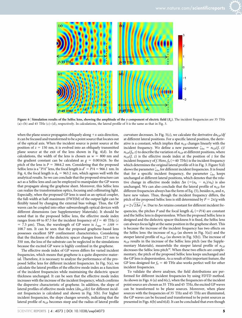
when the plane source propagates obliquely along 1x-axis direction,it can be focused and transformed to be a point source that locates outof the optical axis. When the incident source is point source at theposition of z 5 150 nm, it is evolved into an obliquely transmittedplane source at the exit of the lens shown in Fig. 4(d). In thecalculations, the width of the lens is chosen as w 5 800 nm andthe gradient constant can be calculated as g 5 0.001626. So thepitch of the lens is P 5 3864.2 nm. Considering that the proposedSelfoc lens is a ‘‘P/4’’ lens, the focal length is d9 5 P/4 5 966.1 nm. InFig. 4, the focal length is d0 5 963.2 nm, which agrees well with theanalytical results. So we can conclude that the proposed structure canact as a Selfoc lens and can be employed to manipulate the GP wavesthat propagate along the graphene sheet. Moreover, this Selfoc lenscan realize the transformation optics, focusing and collimating light.Especially, when the proposed GP lens is used as an optical coupler,the full-width at half-maximum (FWHM) of the output light can beflexibly tuned by changing the external bias voltage. Thus, the GPwaves can be coupled into other subwavelength optical devices withdifferent dimensions (see Supplementary Materials). It should benoted that in the proposed Selfoc lens, the effective mode indexranges from 69 to 87.5 for the incident frequency of f 5 40 THz (l5 7.5 mm). Thus, the wavelength of GP wave is lspp 5 l/69 5
108.7 nm. It can be seen that the proposed graphene-based lenspossesses excellent SPP confinement characteristics. Consideringthat the thickness of the dielectric spacer changes from 217 nm to350 nm, the loss of the substrate can be neglected in the simulationsbecause the excited GP wave is highly confined in the graphene.
The effective mode index of GP waves differs for varied incidentfrequencies, which means that graphene is a quite dispersive mater-ial. Therefore, it is necessary to analyze the performance of the pro-posed Selfoc lens for different incident frequencies. In Fig. 5(a), wecalculate the lateral profiles of the effective mode index as a functionof the incident frequencies while maintaining the dielectric spacerthickness unchanged. It can be seen that the effective mode indexincreases with the increase of the incident frequency, which confirmsthe dispersive characteristic of graphene. In addition, the slope oflateral profiles of effective mode index (dnGP/dz) for different incid-ent frequencies is calculated and shown in Fig. 5(b). For higherincident frequencies, the slope changes severely, indicating that thelateral profile of nGP becomes steep and the radius of lateral profile
curvature decreases. In Fig. 5(c), we calculate the derivative dnGP/dfat different lateral positions. For a specific lateral position, the deriv-ative is a constant, which implies that nGP changes linearly with theincident frequency. We define a new parameter ffre 5 nGP(f, z)/nGP(f0, z) to describe the variation of nGP at different positions, wherenGP(f, z) is the effective mode index at the position of z for theincident frequency of f. Here, f0 (540 THz) is the incident frequencywhich determines the original lateral profile of h in Fig. 3. Figure 5(d)shows the parameter ffre for different incident frequencies. It is foundthat for a specific incident frequency, the parameter ffre keepsunchanged at different lateral positions, which denotes that the rela-tive change in effective mode index Dn (5(n0 2 n1)/n0) is alsounchanged. We can also conclude that the lateral profile of nGP fordifferent frequencies always has the form of Eq. (5), besides n0 and n1
have new values. Thus, though the incident frequency differs, thepitch of the proposed Selfoc lens is still determined by P 5 2p/g with
g~2ffiffiffiffiffiffiffiffiffi2Dnp .
w. Due to Dn retains constant for different incident fre-
quencies, the pitches P and the focal length d0 (5P/4) are constantand the Selfoc lens is dispersionless. When the proposed Selfoc lens isdesigned and the dielectric spacer thickness h is fixed, the Selfoc lenscan always focus light at the same position in the graphene sheet. Thisis because the increase of the incident frequency has two effects onthe Selfoc lens: the increase of nGP (as shown in Fig. 5(a)) and thesteeper lateral profile of nGP (as shown in Fig. 5(b)). The increase ofnGP results in the increase of the Selfoc lens pitch (see the Supple-mentary Materials), meanwhile the steeper lateral profile of nGP
decreases the Selfoc lens pitch39. When these two effects are comple-mentary, the pitch of the proposed Selfoc lens keeps unchanged andthe GP lens is dispersionless. As a result of this important feature, theGP lens designed for f0 5 40 THz also works perfect well for otherincident frequencies.
To validate the above analyses, the field distributions are per-formed for different incident frequencies by using FDTD method.As shown in Figs. 6 (a) and 6(c), when the frequencies of the incidentpoint source are chosen as 35 THz and 45 THz, the excited GP wavescan be transformed to be plane sources. Moreover, when planesources with the frequencies of 35 THz and 45 THz are illuminated,the GP waves can be focused and transformed to be point sources aspresented in Figs. 6(b) and 6(d). It can be concluded that even though
Figure 6 | Simulation results of the Selfoc lens, showing the amplitude of the y component of electric field (Ey). The incident frequencies are 35 THz
(a)–(b) and 45 THz (c)–(d), respectively. In calculations, the lateral profile of h is the same as that in Fig. 3.
www.nature.com/scientificreports
SCIENTIFIC REPORTS | 4 : 4073 | DOI: 10.1038/srep04073 5
the Selfoc lens is designed for 40 THz, it can still work well for otherincident frequencies. In addition, the focal lengths for the incidentfrequencies of 35 THz and 45 THz are d1 5 963.1 nm and d2 5
963.5 nm, respectively. While for the frequency of 40 THz, the focallength is d0 5 963.2 nm. It is found that the focal lengths for thesethree incident frequencies are nearly unchanged, which confirmsthat the proposed Selfoc lens is dispersionless. This important char-acteristic ensures that the Selfoc lens possesses a wide operatingfrequency regime, which is necessary in practical applications. Itshould be noted that the pitch of graphene-based Selfoc lens is alsoa constant for different external voltages, which is discussed in theSupplementary Materials.
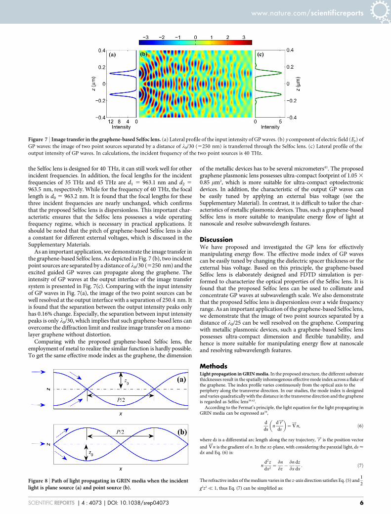
As an important application, we demonstrate the image transfer inthe graphene-based Selfoc lens. As depicted in Fig. 7 (b), two incidentpoint sources are separated by a distance of l0/30 (5250 nm) and theexcited guided GP waves can propagate along the graphene. Theintensity of GP waves at the output interface of the image transfersystem is presented in Fig. 7(c). Comparing with the input intensityof GP waves in Fig. 7(a), the image of the two point sources can bewell resolved at the output interface with a separation of 250.4 nm. Itis found that the separation between the output intensity peaks onlyhas 0.16% change. Especially, the separation between input intensitypeaks is only l0/30, which implies that such graphene-based lens canovercome the diffraction limit and realize image transfer on a mono-layer graphene without distortion.
Comparing with the proposed graphene-based Selfoc lens, theemployment of metal to realize the similar function is hardly possible.To get the same effective mode index as the graphene, the dimension
of the metallic devices has to be several micrometers41. The proposedgraphene plasmonic lens possesses ultra-compact footprint of 1.05 30.85 mm2, which is more suitable for ultra-compact optoelectronicdevices. In addition, the characteristic of the output GP waves canbe easily tuned by applying an external bias voltage (see theSupplementary Material). In contrast, it is difficult to tailor the char-acteristics of metallic plasmonic devices. Thus, such a graphene-basedSelfoc lens is more suitable to manipulate energy flow of light atnanoscale and resolve subwavelength features.
DiscussionWe have proposed and investigated the GP lens for effectivelymanipulating energy flow. The effective mode index of GP wavescan be easily tuned by changing the dielectric spacer thickness or theexternal bias voltage. Based on this principle, the graphene-basedSelfoc lens is elaborately designed and FDTD simulation is per-formed to characterize the optical properties of the Selfoc lens. It isfound that the proposed Selfoc lens can be used to collimate andconcentrate GP waves at subwavelength scale. We also demonstratethat the proposed Selfoc lens is dispersionless over a wide frequencyrange. As an important application of the graphene-based Selfoc lens,we demonstrate that the image of two point sources separated by adistance of l0/25 can be well resolved on the graphene. Comparingwith metallic plasmonic devices, such a graphene-based Selfoc lenspossesses ultra-compact dimension and flexible tunability, andhence is more suitable for manipulating energy flow at nanoscaleand resolving subwavelength features.
MethodsLight propagation in GRIN media. In the proposed structure, the different substratethicknesses result in the spatially inhomogenous effective mode index across a flake ofthe graphene. The index profile varies continuously from the optical axis to theperiphery along the transverse direction. In our studies, the mode index is designedand varies quadratically with the distance in the transverse direction and the grapheneis regarded as Selfoc lens39,42.
According to the Fermat’s principle, the light equation for the light propagating inGRIN media can be expressed as39,
dds
nd r!ds
� �~+!
n, ð6Þ
where ds is a differential arc length along the ray trajectory, r! is the position vector
and +!
n is the gradient of n. In the xz-plane, with considering the paraxial light, ds <dx and Eq. (6) is:
nd2zdx2
~dndz
{dndx
dzdx: ð7Þ
The refractive index of the medium varies in the z-axis direction satisfies Eq. (5) and12
g2z2 = 1, thus Eq. (7) can be simplified as:
Figure 8 | Path of light propagating in GRIN media when the incidentlight is plane source (a) and point source (b).
Figure 7 | Image transfer in the graphene-based Selfoc lens. (a) Lateral profile of the input intensity of GP waves. (b) y component of electric field (Ey) of
GP waves: the image of two point sources separated by a distance of l0/30 (5250 nm) is transferred through the Selfoc lens. (c) Lateral profile of the
output intensity of GP waves. In calculations, the incident frequency of the two point sources is 40 THz.
www.nature.com/scientificreports
SCIENTIFIC REPORTS | 4 : 4073 | DOI: 10.1038/srep04073 6

d2zdx2
~{g2z, ð8Þ
the general solution of Eq. (8) is
z~B cos gxð ÞzC sin gxð Þ, ð9Þ
where B and C are constants determined by the initial conditions. According to Eq.(9), the slope of light line can be derived as,
K~dzdx
~{Bg sin (gx)zCg cos (gx): ð10Þ
Here, the initial conditions are assumed as (K0, z0), which means that the slope andposition of the incident light is K0 and z0, respectively. By solving Eqs. (9) and (10), theconstants B and C are calculated as B 5 z0, C 5 K0/g, then Eq. (9) can be obtained as,
z~z0 cos gxð Þz K0=gð Þ sin gxð Þ: ð11Þ
When the incident light at the position of z0 is plane wave parallel to the optical axis(i.e., the initial conditions are K0 5 0 and z 5 z0), according to Eq. (11), we can get thelight equation
z~z0 cos (gx), ð12Þ
which means that the light propagating in GRIN media follows a cosinoidal path andthe period (also called ‘‘pitch’’) of the Selfoc lens is P 5 2p/g.
As the examples, the path of the light propagating in GRIN media is shown in Fig. 8.It can be seen that when the proposed Selfoc lens is used as an optical coupler, thelength of the lens should be P/4. When it is used to realize the image transfer, thelength of the lens should be P/2.
When the effective mode index has an increment of Dn, by solving the aboveequations, the pitch of the Selfoc lens can be easily obtained as,
P0~2p
g
ffiffiffiffiffiffiffiffiffiffiffiffiffiffinzDn
n0
s: ð13Þ
It can be seen that the pitch of the Selfoc lens increases with the increase of effectivemode index.
1. Barnes, W. L., Dereux, A. & Ebbesen, T. W. Surface plasmon subwavelengthoptics. Nature 424, 824–830 (2003).
2. Gramotnev, D. K. & Bozhevolnyi, S. I. Plasmonics beyond the diffraction limit.Nat. Photon. 4, 83–91 (2010).
3. Oulton, R. F., Sorger, V. J., Genov, D. A., Pile, D. F. P. & Zhang, X. A hybridplasmonic waveguide for subwavelength confinement and long-rangepropagation. Nat. Photon. 2, 496–500 (2008).
4. Leno, I. D. & Berini, P. Amplification of long-range surface plasmons by a dipolargain medium. Nat. Photon. 4, 382–387 (2010).
5. He, S., He, Y. & Jin, Y. Revealing the truth about ‘trapped rainbow’ storage of lightin metamaterials. Sci. Rep. 2, 583; DOI:10.1038/srep00583 (2012).
6. Gan, Q., Ding, Y. J. & Bartoli, F. J. ‘Rainbow’ trapping and releasing attelecomwavelengths. Phys. Rev. Lett. 102, 056801 (2009).
7. Hu, H., Ji, D., Zeng, X., Liu, K. & Gan, Q. Rainbow trapping in hyperbolicmetamaterial waveguide. Sci. Rep. 3, 1249; DOI:10.1038/srep01249 (2013).
8. Wang, G., Lu, H. & Liu, X. Trapping of surface plasmon waves in graded gratingwaveguide system. Appl. Phys. Lett. 101, 013111 (2012).
9. Koppens, F. H. L., Chang, D. E. & Abajo, F. J. G. d. Graphene plasmonics: aplatform for strong light-matter interaction. Nano Lett. 11, 3370–3377 (2011).
10. Fang, Z. et al. Gated tunability and hybridization of localized plasmons innanostructured graphene. ACS Nano 3, 2388–2395 (2013).
11. Geim, A. K. & Novoselov, K. S. The rise of graphene. Nat. Mater. 6, 183–191(2007).
12. Wang, W., Apell, S. P. & Kinaret, J. M. Edge magnetoplasmons and the opticalexcitations in graphene disks. Phys. Rev. B 86, 125450 (2012).
13. Fallahi, A. & Perruisseau-Carrier, J. Design of tunable biperiodic graphenemetasurfaces. Phys. Rev. B 86, 195408 (2012).
14. Jablan, M., Buljan, H. & Soljacic, M. Plasmonics in graphene at infraredfrequencies. Phys. Rev. B 80, 245435 (2009).
15. Vakil, A. & Engheta, N. Transformation optics using graphene. Science 332,1291–1294 (2011).
16. Wang, B., Zhang, X., Yuan, X. & Teng, J. Optical coupling of surface plasmonsbetween graphene sheets. Appl. Phys. Lett. 100, 131111 (2012).
17. Grigorenko, A. N., Polini, M. & Novoselov, K. S. Graphene plasmonics. Nat.Photon. 6, 749–758 (2012).
18. Ju, L. et al. Graphene plasmonics for tunable Terahertz metamaterials. Nat.Nanotechnol. 6, 630–634 (2011).
19. Fallahi, A. & Perruisseau-Carrier, J. Design of tunable biperiodic graphenemetasurfaces. Phys. Rev. B 86, 195408 (2012).
20. Yao, Y. et al. Broad Electrical Tuning of Graphene-Loaded Plasmonic Antennas.Nano Lett. 13, 1257–1264 (2013).
21. Liu, M. et al. A graphene-based broadband optical modulator. Nature 474, 64–67(2011).
22. Lee, S. H. et al. Switching terahertz waves with gate-controlled active graphenemetamaterials. Nat. Mater. 11, 936–941 (2012).
23. Yan, H. et al. Tunable infrared plasmonic devices using graphene/insulator stacks.Nat. Nanotechnol. 7, 330–334 (2012).
24. Yan, H., Xia, F., Li, Z. & Avouris, P. Plasmonics of coupled graphene micro-structures. New J. Phys. 14, 125001 (2012).
25. Wang, B., Zhang, X., Garcıa-Vidal, F. J., Yuan, X. & Teng, J. Strong coupling ofsurface plasmon polaritons in monolayer graphene sheet arrays. Phys. Rev. Lett.109, 073901 (2012).
26. Tamagnone, M., Gomez-Dıaz, J. S., Mosig, J. R. & Perruisseau-Carrier, J.Reconfigurable terahertz plasmonic antenna concept using a graphene stack.Appl. Phys. Lett. 101, 214102 (2012).
27. Chen, J. et al. Optical nano-imaging of gate-tunable graphene plasmons. Nature487, 77–81 (2012).
28. Liu, Y., Zentgraf, T., Bartal, G. & Zhang, X. Transformational Plasmon Optics.Nano Lett. 10, 1991–1997 (2010).
29. Zentgraf, T., Liu, Y., Mikkelsen, M. H., Valentine, J. & Zhang, X. PlasmonicLuneburg and Eaton lenses. Nat. Nanotechnol. 6, 151–155 (2011).
30. Valle, G. D. & Longhi, S. Graded index surface-plasmon-polariton devices forsubwavelength light management. Phys. Rev. B 82, 153411 (2010).
31. Gu, X., Lin, I. & Liu, J. Extremely confined terahertz surface plasmon-polaritons ingraphene-metal structures. Appl. Phys. Lett 103, 071103 (2013).
32. Chen, P.-Y. & Alu, A. Atomically thin surface cloak using graphene monolayers.ACS Nano 5, 5855–5863 (2011).
33. Gan, C. H., Chu, H. S. & Li, E. P. Synthesis of highly confined surface plasmonmodes with doped graphene sheets in the midinfrared and terahertz frequencies.Phys. Rev. B 85, 125431 (2012).
34. Hanson, G. W. Dyadic Green’s functions and guided surface waves for a surfaceconductivity model of graphene. J. Appl. Phys. 103, 064302 (2008).
35. Gao, W., Shu, J., Qiu, C. & Xu, Q. Excitation of plasmonic waves in graphene byguided-mode resonances. ACS Nano 6, 7806–7813 (2012).
36. Fei, Z. et al. Gate-tuning of graphene plasmons revealed by infrared nano-imaginginfrared nano-imaging. Nature 487, 82–85 (2012).
37. Bolotin, K. I. et al. Ultrahigh electron mobility in suspended graphene. Solid StateCommun. 146, 351–355 (2008).
38. Novoselov, K. S. et al. Electric field effect in atomically thin carbon films. Science306, 666–669 (2004).
39. Marchand, E. W. Gradient Index Optics (Academic press, New York, 1978).40. Mao, Y., Chang, S., Sherif, S. & Flueraru, C. Graded-index fiber lens proposed for
ultrasmall probes used in biomedical imaging. Appl. Opt. 46, 5887–5894 (2007).41. Andryieuski, A., Lavrinenko, A. & Chigrin, D. Graphene hyperlens for terahertz
radiation. Phys. Rev. B 86, 121108(R) (2012).42. Agrawal, G. P. Applications of Nonlinear Fiber Optics. (Academic Press, San
Diego, 2001).
AcknowledgmentsThis work was supported by the National Natural Science Foundation of China underGrants 10874239, 10604066, 61223007, and 11204368. We are grateful to Dr. Bingli Zhu,Dr. Jian Liang, Dr. Kai Liu and Dr. Zhaolu Wang for helpful suggestions.
Author contributionsG.W. conceived the idea, completed the numerical simulation, and wrote the manuscripttext. X.L. discussed the design of the proposed structure and simulation results, andsupervised the whole project. H.L. improved the manuscript presentation. C.Z. carried outthe data analysis and prepared part figures. All authors discussed the results andsubstantially contributed to the manuscript.
Additional informationSupplementary information accompanies this paper at http://www.nature.com/scientificreports
Competing financial interests: The authors declare no competing financial interests.
How to cite this article: Wang, G.X., Liu, X.M., Lu, H. & Zeng, C. Graphene plasmonic lensfor manipulating energy flow. Sci. Rep. 4, 4073; DOI:10.1038/srep04073 (2014).
This work is licensed under a Creative Commons Attribution-NonCommercial-NoDerivs 3.0 Unported license. To view a copy of this license,
visit http://creativecommons.org/licenses/by-nc-nd/3.0
www.nature.com/scientificreports
SCIENTIFIC REPORTS | 4 : 4073 | DOI: 10.1038/srep04073 7