graphene growth, doping, and characterization for …
TRANSCRIPT

GRAPHENE GROWTH, DOPING, AND CHARACTERIZATION FOR DEVICEAPPLICATIONS
By
KARA BERKE
A DISSERTATION PRESENTED TO THE GRADUATE SCHOOLOF THE UNIVERSITY OF FLORIDA IN PARTIAL FULFILLMENT
OF THE REQUIREMENTS FOR THE DEGREE OFDOCTOR OF PHILOSOPHY
UNIVERSITY OF FLORIDA
2013

c⃝ 2013 Kara Berke
2

This dissertation is dedicated to Andrew Butchko.
3

ACKNOWLEDGMENTS
I would like to acknowledge the help I have received from other members of my
laboratory and from my collaborators. Particularly, I would like to acknowledge the
guidance given to me at the beginning of my doctoral research by Sefaattin Tongay.
Sefaattin gave a considerable amount of time to training me in laboratory procedures.
He has also has provided valuable insights into the scientific principles behind some
aspects of my work. My fellow lab member Xiaochang Miao has also helped me
considerably through our discussions of fundamental physical principles.
Most recently, I have had the opportunity to work with Prof. Bill Appleton from the
University of Florida’s Materials Science Department, and Xiaotie Wang from Prof. Fan
Ren’s group in the Chemical Engineering Department. They both have contributed to
my work with graphene growth on silicon carbide substrates. Also, I would like to thank
Dinesh Venkatachalam and Rob Elliman of the Australian National University and Joel
Fridmann of Raith USA, Incorporated, for their assistance ion implanting SiC substrates.
I would like to thank those people who have helped by providing sample materials
and measurements. First, Zahra Nasrollahi from Prof. D. B. Tanner’s group in the
University of Florida’s Physics Department conducted transmittance measurements
reported in Chapter 3. Solar cell fabrication and characterization mentioned in Chapter
3 were performed by Xiaochang Miao and Maureen Petterson (Physics Department,
University of Florida, Prof. Andrew Rinzler’s lab). Mitch McCarthy (also Prof. Andrew
Rinzler’s lab) helped provide expertise in the application of organic materials used in
Chapter 4. TEM images of annealed samples (Chapter 5) were provided by Nicholas
Rudawski (University of Florida, Materials Science Department) and has helped in the
interpretation of these images.
I would like to thank the members of my doctoral committee: Prof. Chris Stanton,
Dr. Brent Gila, Prof. Andrew Rinzler, and Prof. Amlan Biswas. Lastly, I would like to
4

acknowledge the support and advice given to me by my research advisor, Prof. A. F.
Hebard.
5

TABLE OF CONTENTS
page
ACKNOWLEDGMENTS . . . . . . . . . . . . . . . . . . . . . . . . . . . . . . . . . . 4
LIST OF TABLES . . . . . . . . . . . . . . . . . . . . . . . . . . . . . . . . . . . . . . 9
LIST OF FIGURES . . . . . . . . . . . . . . . . . . . . . . . . . . . . . . . . . . . . . 10
ABSTRACT . . . . . . . . . . . . . . . . . . . . . . . . . . . . . . . . . . . . . . . . . 12
CHAPTER
1 INTRODUCTION TO GRAPHENE . . . . . . . . . . . . . . . . . . . . . . . . . 14
1.1 Introduction . . . . . . . . . . . . . . . . . . . . . . . . . . . . . . . . . . . 141.2 History . . . . . . . . . . . . . . . . . . . . . . . . . . . . . . . . . . . . . . 151.3 Crystal Structure of Graphene . . . . . . . . . . . . . . . . . . . . . . . . 16
1.3.1 The Graphene Lattice . . . . . . . . . . . . . . . . . . . . . . . . . 161.3.2 Hybridized Orbitals . . . . . . . . . . . . . . . . . . . . . . . . . . . 18
1.4 Electronic Structure of Graphene . . . . . . . . . . . . . . . . . . . . . . . 211.4.1 Tight Binding Model . . . . . . . . . . . . . . . . . . . . . . . . . . 211.4.2 Density of States . . . . . . . . . . . . . . . . . . . . . . . . . . . . 24
1.5 Growth . . . . . . . . . . . . . . . . . . . . . . . . . . . . . . . . . . . . . 251.5.1 Mechanical Exfoliation . . . . . . . . . . . . . . . . . . . . . . . . . 251.5.2 Chemical Vapor Deposition . . . . . . . . . . . . . . . . . . . . . . 251.5.3 Epitaxial Growth on SiC . . . . . . . . . . . . . . . . . . . . . . . . 26
1.6 Device Applications: Schottky Junctions . . . . . . . . . . . . . . . . . . . 261.6.1 Metal/n-Type Semiconductor Junctions . . . . . . . . . . . . . . . . 271.6.2 Metal/p-Type Semiconductor Junctions . . . . . . . . . . . . . . . . 281.6.3 The Diode Equation and J-V Relations in Schottky Junctions . . . 29
2 EXPERIMENTAL METHODS . . . . . . . . . . . . . . . . . . . . . . . . . . . . 31
2.1 Graphene Synthesis by Chemical Vapor Deposition . . . . . . . . . . . . 312.2 Raman Spectroscopy . . . . . . . . . . . . . . . . . . . . . . . . . . . . . 33
2.2.1 The Raman Process . . . . . . . . . . . . . . . . . . . . . . . . . . 332.2.2 Phonons in Graphene . . . . . . . . . . . . . . . . . . . . . . . . . 342.2.3 The Graphene Raman Spectrum . . . . . . . . . . . . . . . . . . . 35
2.2.3.1 Characteristic Peaks . . . . . . . . . . . . . . . . . . . . . 352.2.3.2 Relative Peak Intensities . . . . . . . . . . . . . . . . . . 40
2.2.4 Determining One Allotrope From Another . . . . . . . . . . . . . . 41
3 STABLE HOLE DOPING OF GRAPHENE FOR LOW ELECTRICAL RESISTANCEAND HIGH OPTICAL TRANSPARENCY . . . . . . . . . . . . . . . . . . . . . . 43
3.1 Electron and Hole Doping in Semiconducting Materials . . . . . . . . . . 433.2 Hole Doping Graphene with TFSA for Optoelectronic Applications . . . . 45
6

3.3 Experimental Details . . . . . . . . . . . . . . . . . . . . . . . . . . . . . . 463.4 Results and Discussion . . . . . . . . . . . . . . . . . . . . . . . . . . . . 48
3.4.1 Reduced Resistivity and Environmental Stability . . . . . . . . . . . 483.4.2 Effects on Carrier Mobility . . . . . . . . . . . . . . . . . . . . . . . 503.4.3 Raman Spectra Before and After Doping . . . . . . . . . . . . . . . 523.4.4 Transmittance Before and After Doping . . . . . . . . . . . . . . . . 54
3.5 Conclusions and Applications . . . . . . . . . . . . . . . . . . . . . . . . . 55
4 CURRENT TRANSPORT ACROSS THE PENTACENE/CVD-GROWN GRAPHENEINTERFACE FOR DIODE APPLICATIONS . . . . . . . . . . . . . . . . . . . . 57
4.1 Introduction . . . . . . . . . . . . . . . . . . . . . . . . . . . . . . . . . . . 574.2 Experimental Details . . . . . . . . . . . . . . . . . . . . . . . . . . . . . . 594.3 Results and Discussion . . . . . . . . . . . . . . . . . . . . . . . . . . . . 60
4.3.1 Pentacene Orientation . . . . . . . . . . . . . . . . . . . . . . . . . 604.3.2 Atmospheric Effects on Diode Performance . . . . . . . . . . . . . 614.3.3 Current Transport Processes Across Rectifying Junctions . . . . . 63
4.3.3.1 Poole-Frenkel Conduction . . . . . . . . . . . . . . . . . . 654.3.3.2 Schottky Barrier Height Lowering in Graphene Diodes . . 70
4.4 Conclusions . . . . . . . . . . . . . . . . . . . . . . . . . . . . . . . . . . . 71
5 ENHANCED GRAPHITIZATION OF SILICON CARBIDE THROUGH SURFACEION IMPLANTATION AND PULSED LASER ANNEALING . . . . . . . . . . . . 74
5.1 Introduction . . . . . . . . . . . . . . . . . . . . . . . . . . . . . . . . . . . 745.1.1 Epitaxial Graphene Growth on SiC . . . . . . . . . . . . . . . . . . 74
5.1.1.1 Growth on the Si-Face . . . . . . . . . . . . . . . . . . . . 765.1.1.2 Growth on the C-Face . . . . . . . . . . . . . . . . . . . . 76
5.2 Site Selective Graphene Growth on SiC Using Ion Implantation . . . . . . 775.2.1 Previous Work . . . . . . . . . . . . . . . . . . . . . . . . . . . . . 775.2.2 Growth in the Absence of Foreign Ionic Species . . . . . . . . . . . 795.2.3 Conclusions . . . . . . . . . . . . . . . . . . . . . . . . . . . . . . . 84
5.3 Future Work: Optimizing Growth Parameters . . . . . . . . . . . . . . . . 845.3.1 Amorphization Depth . . . . . . . . . . . . . . . . . . . . . . . . . . 855.3.2 Number of Pulses . . . . . . . . . . . . . . . . . . . . . . . . . . . . 905.3.3 Sample Environment During PLA . . . . . . . . . . . . . . . . . . . 905.3.4 Ionic Species . . . . . . . . . . . . . . . . . . . . . . . . . . . . . . 91
APPENDIX
A GRAPHENE’S BAND STRUCTURE WITHIN THE TIGHT BINDING MODEL . 94
B THERMAL ANALYSIS OF PULSED LASER ANNEALING . . . . . . . . . . . . 96
REFERENCES . . . . . . . . . . . . . . . . . . . . . . . . . . . . . . . . . . . . . . . 101
BIOGRAPHICAL SKETCH . . . . . . . . . . . . . . . . . . . . . . . . . . . . . . . . 106
7

LIST OF TABLES
Table page
5-1 Parameters used in numerical analysis for SiC. . . . . . . . . . . . . . . . . . . 84
5-2 Ion Implantation Conditions . . . . . . . . . . . . . . . . . . . . . . . . . . . . . 85
8

LIST OF FIGURES
Figure page
1-1 Translational vectors of the graphene lattice in real space . . . . . . . . . . . . 16
1-2 Translational vectors of the graphene lattice in reciprocal space . . . . . . . . . 17
1-3 Visualization of the electron occupation in Be before and after sp hybridization.. . . . . . . . . . . . . . . . . . . . . . . . . . . . . . . . . . . . . . . . . . . . . 19
1-4 Visualization of the electron occupation in B before and after sp2 hybridization.. . . . . . . . . . . . . . . . . . . . . . . . . . . . . . . . . . . . . . . . . . . . . 19
1-5 Orbital geometries of hybridized orbitals and the bonds between them. . . . . . 20
1-6 Visualization of the electron occupation in C before and after sp3 hybridization.. . . . . . . . . . . . . . . . . . . . . . . . . . . . . . . . . . . . . . . . . . . . . 21
1-7 Energy band diagram of an n-type Schottky junction. . . . . . . . . . . . . . . . 27
1-8 Energy band diagram of an n-type Schottky junction with an applied bias. . . . 28
1-9 Energy band diagram of a p-type Schottky junction. . . . . . . . . . . . . . . . 29
2-1 The CVD growth process used to grow and transfer graphene onto a desiredsubstrate. . . . . . . . . . . . . . . . . . . . . . . . . . . . . . . . . . . . . . . . 32
2-2 Schematic representations of light-matter interactions. . . . . . . . . . . . . . . 34
2-3 Graphene Phonons . . . . . . . . . . . . . . . . . . . . . . . . . . . . . . . . . 36
2-4 Schematic representation of the scattering processes corresponding to the Gpeak and the 2D peak. . . . . . . . . . . . . . . . . . . . . . . . . . . . . . . . . 37
2-5 Schematic representation of the double resonant Raman scattering processesresponsible for the D and D′ peaks, and the triple resonant process contributingto the 2D peak. . . . . . . . . . . . . . . . . . . . . . . . . . . . . . . . . . . . . 39
2-6 Raman spectra of graphene and graphene related materials . . . . . . . . . . . 40
2-7 The second order Raman scattering process . . . . . . . . . . . . . . . . . . . 42
3-1 Energy band structure after conventional doping . . . . . . . . . . . . . . . . . 44
3-2 Energy band structure before and after surface charge transfer doping. . . . . 45
3-3 Sample geometry and undoped Raman spectra . . . . . . . . . . . . . . . . . . 47
3-4 Scanning electron microscope (SEM) images . . . . . . . . . . . . . . . . . . . 48
3-5 Electrical measurements taken before and after doping with TFSA. . . . . . . . 50
9

3-6 Raman spectrum taken at different spots on the graphene/sapphire (SiO2)samples before and after doping. . . . . . . . . . . . . . . . . . . . . . . . . . . 53
3-7 Transmittance versus wavelength . . . . . . . . . . . . . . . . . . . . . . . . . . 54
4-1 Schematic diagram of Au/Pentacene/Graphene diodes. . . . . . . . . . . . . . 58
4-2 X-ray diffraction data and AFM images for pentacene on graphene, Cu, andHOPG . . . . . . . . . . . . . . . . . . . . . . . . . . . . . . . . . . . . . . . . . 61
4-3 J-V characteristics before and after exposure to ambient atmosphere . . . . . 64
4-4 J-V analysis for transport via thermionic emission and Poole-Frenkel conduction. 66
4-5 Raman data . . . . . . . . . . . . . . . . . . . . . . . . . . . . . . . . . . . . . . 69
5-1 Cross sectional view of 4H and 6H SiC structures. Samples can be cleavedto reveal Si-terminated (0001), and a C-terminated (000�1) surfaces. . . . . . . 75
5-2 Raman spectrum taken before and after pulsed laser anneals (PLA) implantedand unimplanted samples at 0.8 J/cm2 for 2000 pulses in Argon . . . . . . . . 80
5-3 Raman spectra taken of implanted and unimplanted samples after PLA at 0.8J/cm2 for 2000 pulses in air, after subtraction of the SiC signal. . . . . . . . . . 81
5-4 Cross-sectional TEM (X-TEM) image of 6H-SiC, amorphized via ion implantationto a depth of 20 nm, after pulse laser annealing at 0.8 J/cm2 for 2000 pulses . 82
5-5 Raman Spectra taken after PLA at 0.8 J/cm2 of samples 1-6 . . . . . . . . . . 86
5-6 Cross-sectional TEM images taken of sample 5 (dα = 124nm) after pulselaser annealing at 0.8 J/cm2 for 100 pulses in air . . . . . . . . . . . . . . . . . 88
5-7 Threshold fluences necessary to raise the surface temperature of a sampleduring a 25 ns pulse to the melting temperature of amorphous SiC, 2445K,versus amorphous layer thickness, dα, of amorphous/crystalline SiC. . . . . . 89
5-8 Raman spectra taken from sample 2 after PLA in air and argon for 1000 pulsesat 0.8 J/cm2. . . . . . . . . . . . . . . . . . . . . . . . . . . . . . . . . . . . . . 90
5-9 6H-SiC implanted with Si and C atoms to produce a 20nm amorphous SiCsurface layer prior to laser annealing at 0.8 J/cm2 for 2000 pulses in air. . . . . 91
5-10 Raman spectra taken after PLA at 0.8 J/cm2 for 2000 pulses in argon of sample2 in regions with and without additional Au+ implants. . . . . . . . . . . . . . . 92
10

Abstract of Dissertation Presented to the Graduate Schoolof the University of Florida in Partial Fulfillment of theRequirements for the Degree of Doctor of Philosophy
GRAPHENE GROWTH, DOPING, AND CHARACTERIZATION FOR DEVICEAPPLICATIONS
By
Kara Berke
December 2013
Chair: Arthur HebardMajor: Physics
This dissertation aims to describe fundamental physics concepts regarding the
fabrication and characterization of graphene for device applications. Ultimately, the goal
of this research is to further knowledge of graphene systems in hopes that commercial
applications can soon be realized. The first chapter introduces the reader to graphene,
beginning with a brief history of its discovery in 2004 and moving on to cover basic
structural and electrical properties. A basic knowledge of solid state physics is assumed.
The second chapter describes some of the common research techniques employed
in subsequent chapters. This includes chemical vapor deposition synthesis methods
used to produce the graphene used in Chapters 3 and 4. Also included is an explanation
of the graphene Raman spectrum. Raman spectroscopy is used extensively throughout
this dissertation, and an understanding of the underlying physical principles is key to
interpreting the data.
In Chapter 3, surface charge transfer is discussed as a means of doping graphene
to increase the density of charge carriers. By treating the graphene surface with the
organic material bis(trifluoromethanesulfonyl)amide (TFSA), the resistivity of the
samples decreases by 70%. We observe a dramatic increase in the hole concentration
after doping, with only minimal reduction of carrier mobility. Raman spectra are
consistent with hole doping, but more importantly indicate that the overall quality of
the graphene is preserved during the process. Transmittance measurements are taken
11

in the visible and near-infrared ranges indicating that TFSA-doping does not significantly
increase overall sample reflectance. This has allowed TFSA-doped graphene to be
implemented into a graphene/n-Si solar cell to achieve a record-breaking 8.6% power
conversion efficency, and shows promise for other optoelectronic applications.
Chapter 4 examines the affect of lattice-matching between graphene and organic
semiconductors on a Schottky Junction diode. In particular, instead of applying an
organic liquid to the graphene surface, the organic small molecule pentacene is
deposited directly onto graphene via thermal vapor deposition. Similarity between
the structure of pentacene and graphene (both are comprised of hexagonal carbon
subunits with approximately the same lattice spacing) allows the first few layers of
pentacene molecules to adopt an orientation nearly parallel to the graphene surface,
whereas pentacene typically adopts a perpendicular orientation when deposited on
metallic substrates. A parallel orientation is preferable for vertical device architectures
as it aligns pentacene’s high mobility axis in the direction of charge transport. However,
diode performance in pentacene/graphene diodes was hindered by a large density of
charge trapping sites near the pentacene/graphene interface, which led to a combination
of Poole-Frenkel transport and thermionic emission; whereas in an ideal schottky diode,
transport is described by thermionic emission alone.
Lastly, Chapter 5 focuses on an alternative graphene growth process through
epitaxial growth on SiC substrates via pulsed laser annealing (PLA). This process
is further refined by using ion implantation as a means to selectively amorphize the
sample surface prior to PLA to achieve graphitic growth in predetermined areas on
the substrate. Raman spectroscopy and transmission electron microscopy are used to
confirm the presence of graphene layers after PLA.
12

CHAPTER 1INTRODUCTION TO GRAPHENE
1.1 Introduction
Since its discovery in 2004 [1], graphene has attracted considerable interest, both
within the scientific community and with the public at large. It has been hailed as a
wonder material with the potential to replace silicon in the semiconductor industry.
Though perhaps these claims are exaggerated, graphene has shown considerable
promise in diodes, transistors, LEDs, and photovoltaic devices due to its unique
properties. With a mean free path on the order of a micron, and charge mobility values
reported up to 230,000 cm2V−1s−1 [2], 1 graphene holds the record for the highest
reported electron mobility of any material. It also has excellent mechanical properties
(breaking another record for its intrinsic strength of 130 GPa [3]), as well as thermal
properties (with a thermal conductivity 5× 10³Wm−1K−1[4]. This work, however, focuses
mainly on graphene’s electrical characteristics. Of particular interest is the graphene
band structure near the K and K′ points 2 , which results in a linear dispersion relation
and a vanishing density of states (DOS) at the Fermi level. Because of the linearity
in graphene’s dispersion relation, its valence and conduction band meet at exactly
one point, making graphene a zero band gap semiconductor, or semi-metal. At the
point where these bands meet (known as the Dirac Point), charge carriers behave
as massless Dirac fermions, accounting for graphene’e high mobility. Near this point,
because the DOS goes to zero, and only a small number of excess charge carriers is
needed to result in a large shift in the graphene Fermi energy. This allows graphene to
be easily n- or p- doped as desired to increase or decrease the graphene work function.
1 For comparison, the mean free path in copper is ∼40 nm and a typical mobility is∼ 45cm2V−1s−1. For Si, the mobility is ∼ 1400cm2V−1s−1
2 K and K′ points are high symmetry points defined by the corners of graphene’s firstBrillouin zone (Section 1.3)
13

These two key attributes make graphene an ideal candidate for device applications that
require a material with both high conductivity and a tunable work function.
1.2 History
Though the band structure of graphene was derived as early as 1947 by P. R.
Wallace[5], at the time, free-standing 2D materials were thought to be thermodynamically
unstable[6, 7]. However, in 2003 a group at Manchester University headed by A. K.
Geim and K. S. Novoselov realized the first monolayer graphene sample through the
mechanical exfoliation of 3D graphite[8]. Originally, Geim had challenged Novoselov
to thin down graphite samples as much as possible. Graphite is comprised of ABAB
stacked (aka Bernal stacked) graphene layers. Bonding between carbon atoms within
each sheet is much stronger than bonding between sheets (along the c-axis). After
applying an adhesive strip to a graphite surface, and gently peeling away the strip3 ,
bonds are preferentially broken between layers, revealing nearly atomically flat a-b
planes. Using this method, Novoselov made thinner and thinner graphite samples, but
he eventually found that the layers of material stuck to the tape that he had initially
discarded were thinner than those he could produce by thinning a bulk material.
Geim and Novoselov were able to transfer flakes from the discarded tape to Si/SiO2
substrates, allowing them to identify monolayer graphene; their work was published the
following year in Science[1].
The seeming conflict between the existence of such a sample with established
theory can be reconciled through either of two arguments: 1) 2D samples are in a
metastable state where their small size and strong interatomic bonds prohibit large
atomic dislocations caused by thermal fluctuations [9, 10]. 2) Samples are not 2D in
the strictest sense; crumpling and warping on the nanometer scale into a 3rd spatial
dimension suppress thermal vibrations[11–13]. Either way, high quality graphene
3 This is the famous ”scotch tape method”
14

Figure 1-1. Translational vectors of the graphene lattice in real space. Blue atomsrepresent atoms within a common sublattice, while atoms in red reside in theother sublattice.
samples were realized, which exhibited the electronic properties of the theorized 2D
graphene including the anomalous quantum Hall effect, which is indicative of massless
Dirac Fermions[8].
1.3 Crystal Structure of Graphene
1.3.1 The Graphene Lattice
Graphene’s structure is often described as a single sheet of carbon atoms in
a hexagonal ”honeycomb” lattice. This lattice is actually made up of two equivalent
sublattices: A and B (Figure 1-1). Primitive vectors for each sublattice can be defined by:
a1 =
√3a
2x+
a
2y, a2 =
√3a
2x− a
2y (1–1)
where a is the lattice constant =2.46 A, describing the minimum spacing between two
atoms on the same sublattice (the distance from one A atom to another A atom or from
one B atom to a second B atom). Note that when both sublattices are considered these
vectors do not indicate the distance to nearest neighbor atoms. Each carbon atom in the
A sublattice has three nearest neighbors, all three of which reside in the B sublattice,
and vice versa. The vectors to each A atom’s nearest neighbors are given by:
15
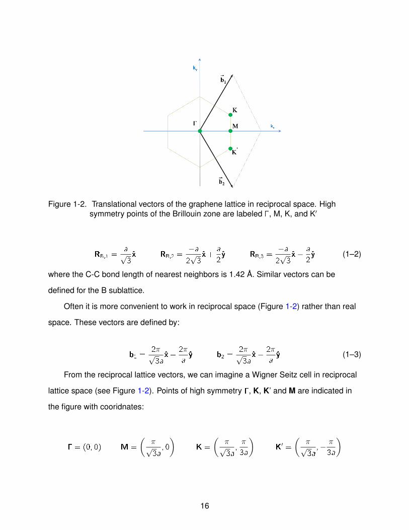
Figure 1-2. Translational vectors of the graphene lattice in reciprocal space. Highsymmetry points of the Brillouin zone are labeled �, M, K, and K′
RB,1 =a√3x RB,2 =
−a2√3x+
a
2y RB,3 =
−a2√3x− a
2y (1–2)
where the C-C bond length of nearest neighbors is 1.42 A. Similar vectors can be
defined for the B sublattice.
Often it is more convenient to work in reciprocal space (Figure 1-2) rather than real
space. These vectors are defined by:
b1 =2π√3ax+
2π
ay b2 =
2π√3ax− 2π
ay (1–3)
From the reciprocal lattice vectors, we can imagine a Wigner Seitz cell in reciprocal
lattice space (see Figure 1-2). Points of high symmetry �, K, K’ and M are indicated in
the figure with cooridnates:
� = (0, 0) M =
(π√3a
, 0
)K =
(π√3a
,π
3a
)K′ =
(π√3a
,− π
3a
)
16

Now let us look at how carbon atoms arranged in this manner interact with each other by
considering the bonds that connect them.
1.3.2 Hybridized Orbitals
Hybridized orbitals occur when it is energetically favorable for atomic orbitals of an
atom to mix with each other. For example, it may be energetically favorable for electrons
to be promoted from the s orbital of an atom to interact with one or more of the p orbitals
of that atom to create sp, sp2, and sp3 hybridized orbitals.
Let’s begin with the simplest of these cases: sp hybridization, in which one s orbital
and one p orbital are mixed. To understand sp orbital hybridization, consider the Be
atom, 1s22s2 (Figure 1-3). In its ground state, Be has 2 electrons in its 1s orbital and
2 electrons in its 2s orbital and thus has two full orbitals. The Be atom in its ground
state does not like to bond with other atoms. In order for a Be atom to form a bond with
another atom, it must promote one of its electrons from the 2s orbital to a 2p orbital.
This process leaves 2 unpaired electrons available for bonding, but now the atom is in
a less energetically favorable state because it no longer has completely filled orbitals.
This problem is somewhat mollified when the 2s and 2p orbital mix to create a half-filled
sp hybrid orbital, which will lower the energy while still allowing two bond sites on the
Be atom. The remaining unfilled p orbitals are unchanged in this process. Using the
conventional Dirac notation, we may represent this mixing of orbitals by:
|sp1⟩ =1√2(|2s⟩+ |2px⟩) (1–4)
|sp2⟩ =1√2(|2s⟩ − |2px⟩) (1–5)
where the px orbital was chosen arbitrarily. The py orbital or pz orbital may just as easily
be chosen in place of the px orbital to represent this interaction, so long as the remaining
two orbitals do not participate in the bond.
17
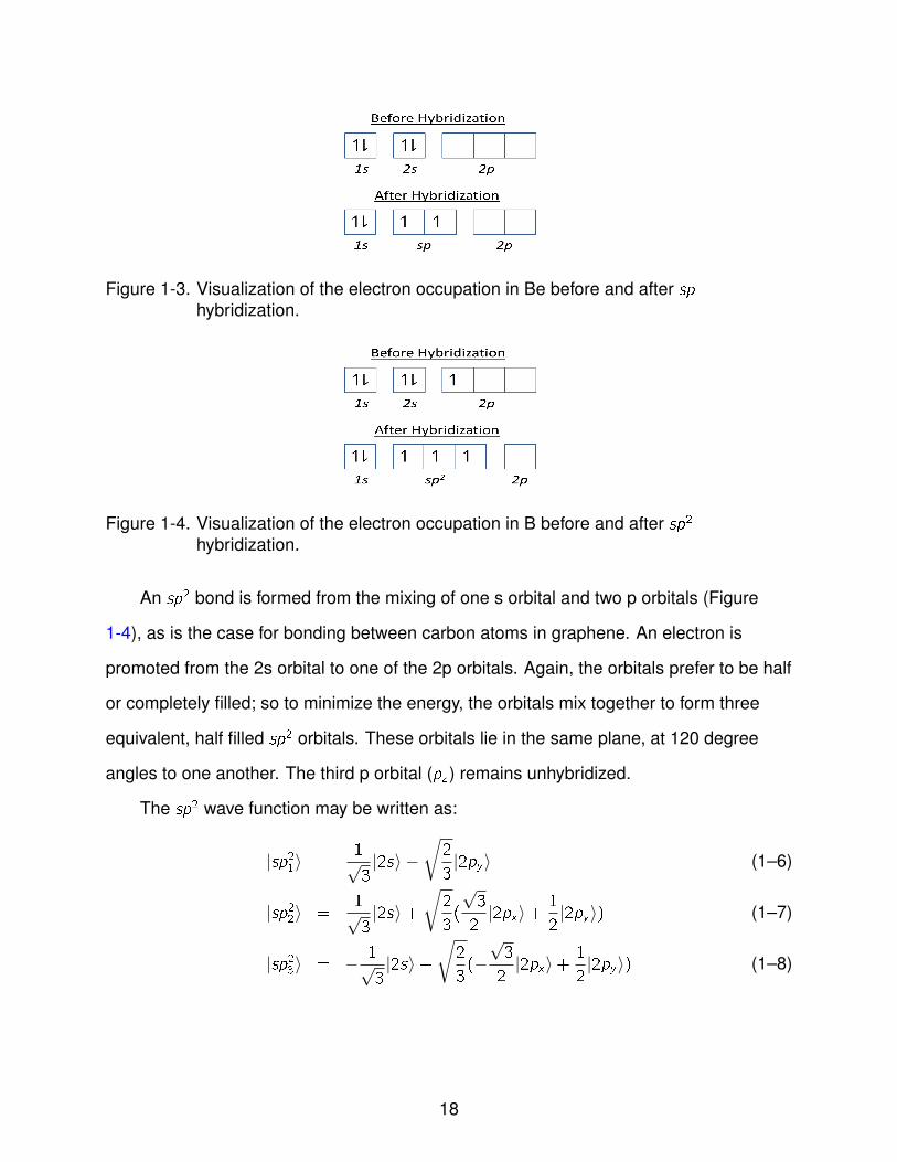
Figure 1-3. Visualization of the electron occupation in Be before and after sphybridization.
Figure 1-4. Visualization of the electron occupation in B before and after sp2
hybridization.
An sp2 bond is formed from the mixing of one s orbital and two p orbitals (Figure
1-4), as is the case for bonding between carbon atoms in graphene. An electron is
promoted from the 2s orbital to one of the 2p orbitals. Again, the orbitals prefer to be half
or completely filled; so to minimize the energy, the orbitals mix together to form three
equivalent, half filled sp2 orbitals. These orbitals lie in the same plane, at 120 degree
angles to one another. The third p orbital (pz ) remains unhybridized.
The sp2 wave function may be written as:
|sp21⟩ =1√3|2s⟩ −
√2
3|2py ⟩ (1–6)
|sp22⟩ =1√3|2s⟩+
√2
3(
√3
2|2px⟩+
1
2|2py ⟩) (1–7)
|sp23⟩ = − 1√3|2s⟩+
√2
3(−
√3
2|2px⟩+
1
2|2py ⟩) (1–8)
18

D E
Figure 1-5. Orbital geometries of hybridized orbitals and the bonds between them. A) sp,B) sp2, and C) sp3 hybridized orbitals. D) Sigma bonds between sp2 orbitals(blue) and E) Sigma bonds between sp2 orbitals (blue) and pi bonds(red)between the unhybridized pz orbitals.
These hybrid orbitals form strong in-plane bonds between adjacent C atoms, which
are referred to as sigma bonds (Figure 1-5 D). The leftover pz orbitals interact with one
another to form weaker π bonds. In a σ bond, one atomic orbital interacts with only
one other orbital, while each of the pz orbitals interacts with three pz orbitals, one from
each of its parent atom’s three nearest neighbors. Each of its parent atom’s nearest
neighbors has a pz orbital that interacts with that atom’s nearest neighbors, and so on.
The π bonds (Figure 1-5 E) are in this way ”smeared out” or delocalized over all the
carbon atoms, whereas the electrons in σ bonds are localized along the axis joining
two adjacent C atoms, and do not interact with the bonding between any other two
atoms. Therefore, in the following section, we only need consider the pz orbitals when
determining the graphene electronic band structure.
It should be noted that though idealized graphene is completely built from sp2
orbitals, defect sites can also allow for the third type of hybridization sp3 orbitals (Figure
19

Figure 1-6. Visualization of the electron occupation in C before and after sp3
hybridization.
1-6). In this type of hybridization, one s orbital mixes with all three p orbitals to form four
equivalent orbitals in a tetragonal configuration (bond angle 109.5 degrees)
1.4 Electronic Structure of Graphene
1.4.1 Tight Binding Model
In this section, solutions to the tight binding model are used to determine the
graphene band structure. 4 The basic assumption behind the tight binding model
is that electrons are tightly bound to a parent atom, and thus Bloch states can be
constructed using the atomic orbitals as a basis. The tight binding Hamiltonian can thus
be described:
Htight−binding = Hatom + �U (1–9)
where Hatom is the unperturbed, well-localized atomic Hamiltonian, and �U is a small
perturbation accounting for the interaction between neighboring atoms. We need only
consider interactions between nearest neighbor atoms to get a good approximation
for the graphene band structure. We can further simplify the calculations by only
considering the pz orbitals as electrons tightly bound between C atoms in sp2 sigma
4 This model was first applied to graphene by Wallace in 1947[5]
20

bonds do not significantly contribute to conduction. This leaves us with only two Bloch
functions to consider, one for each sublattice:
�A =1√N
3∑m
e ik·RA,mϕ(r − RA,m) (1–10)
�B =1√N
3∑n
e ik·RB,nϕ(r − RB,n) (1–11)
where RA,m are the vectors given by Equation 1–2 in Section 1.3. Inserting ⟨ϕpz ,A| and
⟨ϕpz ,B | states into the Schrodinger equation, and considering only nearest-neighbor
interactions, we may write the secular equation for our system in terms of 2x2 matrices:HAA HBA
HBA HBB
= E
SAA SBA
SBA SBB
(1–12)
with elements:
HAA =1
N
∑RA
∑RA
e ik·(RA−RA)⟨ϕpz ,A(r − RA)|Hatom|ϕpz ,A(r − RA)⟩ = ϵpz (1–13)
HAB =1
N
∑RA
∑RB
e ik·(RB−RA)⟨ϕpz ,A(r − RA)|�U|ϕpz ,B(r − RB)⟩ (1–14)
= (e ik·R(A−B)1 + e ik·R(A−B)2 + e ik·R(A−B)3)⟨ϕpz ,A(r − RA)|�U|ϕpz ,B(r − RA − RA−Bj)⟩(1–15)
where in the last step, we choose to sum only over nearest neighbor atoms. We may
similarly determine the overlap integral components, Sm,n = ⟨�A|�B⟩, with sm,n =
⟨ϕA|ϕB⟩. We further define
f (k) = e ik·R(A−B)1 + e ik·R(A−B)2 + e ik·R(A−B)3 (1–16)
t = ⟨ϕA(r − RA)|�U|ϕB(r − RA − RA−Bj)⟩ (1–17)
21

so that we can concisely rewrite the Hamiltonian and resulting secular equation
ϵpz tf (k)
tf (k)∗ ϵpz
= E
1 sf (k)
sf (k)∗ 1
(1–18)
with solution:
E =ϵpz ± t
√|f (k)|2
1± s√
|f (k)|2(1–19)
When Si =j is set to 0, the resulting energy levels can be described by:
E± = ϵ2pz ± γ
√1 + 4cos(
kx√3a
2)cos(
kya
2) + 4cos2(
kya
2) (1–20)
At high symmetry points �, M, and K points, the values are ±3γ, ±γ, and 0 respectively.
Note that this implies a 0 energy gap between conduction and valence bands (Eg =
ϵpzA−ϵpzB) owing to the fact that atoms on the A and B atoms are distinct, but equivalent.
Near the K and K’ points, this expression can be simplified to:
E± = ±~vF |k | (1–21)
where ~ is plank’s constant and vF is the Fermi velocity defined by vF = 3γ/2~ ≈
106m/s .
Equation 1–21 has profound consequences on graphene’s electronic properties. It
defines graphene’s valence and conduction bands near the K and K’ points to be linear,
meeting at exactly one point. At this point, known as the Dirac point for reasons we will
see shortly, the graphene Fermi level, EF is zero and so graphene is neutral. Symmetry
of the bands around the Dirac point implies electrons and holes in graphene should
travel with equal group velocities. Moreover, because the dispersion relation results in
linear, rather than the typical quadratic band structure, the Dirac point essentially has
infinite curvature, and thus charge carriers at this point should have a zero effective
mass.
22

To further ellucidate the massless nature of charge carriers at this point, consider
the Hamiltonian for the Dirac equation in the limit of zero mass:
H = −i~vσ · ∇ (1–22)
where σ represents the Pauli matrices σ = (σx ,σy). Now consider the graphene
Hamiltonian near the K and K’ points:
H = ~vF
0 kx − iky
kx + iky 0
= ~vFσ · k (1–23)
The striking similarity between these two equations clearly shows the massless nature
of electrons near the K and K’ points in ideal graphene. Its eigenfunctions resemble the
4 component spinor solutions of the Dirac Hamiltonian, but with K and K’ degeneracy in
place of spin degeneracy. Therefore, the position of an electron on either sublattice A
or sublattice B can be thought of as a pseudospin. More on this subject is beyond the
scope of this thesis. The interested reader may refer to X. Miao’s dissertation [14].
1.4.2 Density of States
In addition to its linear dispersion relation, graphene also exhibits a vanishing
density of states near the Fermi level. Unlike conventional 3D materials where DOS3D ∼√E , or even in conventional 2D materials where DOS2D is a constant, graphene’s DOS
varies linearly with E, which in turn is proportional to√n.
Therefore, when E goes to 0 at the Fermi level, the DOS also goes to zero. The
square root dependence on the density of states results in a large energy shift even for
a small change in n. Consequently, graphene can be easily electron (n-type) doped or
hole (p-type) doped. This is useful in device applications as adding charge carriers to
the system can increase graphene’s conductivity as well as tune its work function.
23

1.5 Growth
Though other methods exist (e.g. unzipping nanotubes, chemical reduction of
graphene oxide, etc.) the three most common methods of obtaining graphene are:
mechanical exfoliation of graphite, chemical vapor deposition (CVD), and epitaxial
growth through thermally annealing SiC substrates.
1.5.1 Mechanical Exfoliation
Mechanical exfoliation, commonly referred to as ”the scotch tape method”, was
the first method discovered for producing graphene. In bulk graphite, graphene layers
are Bernal (ABAB) stacked on top of one another. Though atoms within each layer
are strongly bound together by in-plane sigma bonds (as described in Section 1.3),
the layers are only weakly bound to one another through Van der Waals forces. Thus,
by applying a small force along the c-axis (perpendicular to the graphene plane) of
graphite, individual layers can be separated from another. Ultimately, a single layer of
graphene can be isolated.
The advantage of this method is that it results in extremely high quality samples. All
of the data regarding the record-breaking properties of graphene (e.g. highest recorded
mobility, etc.) were taken from measurements of exfoliated graphene samples. The
disadvantage of this technique lies in its scalability. The size of the samples produced
through mechanical exfoliation is typically on the order of microns or smaller. This
severely limits their integration into devices.
1.5.2 Chemical Vapor Deposition
Most often, chemical vapor deposition for graphene growth begins with Cu foils,
which are are heated to high temperatures under the flow of hydrogen and and a
carbon containing gas, such as methane. The hydrogen acts to crack the bonds in the
carbonaceous gas; disassociated carbon atoms land on the foil surface. A catalytic
reaction between the C atoms and Cu substrates facilitates the rearrangement of C
atoms to form a monolayer of graphene on both sides of the Cu foil. Graphitic growth
24
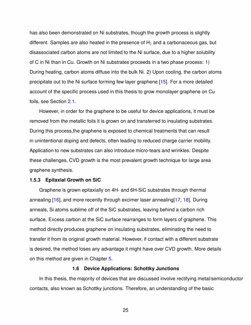
has also been demonstrated on Ni substrates, though the growth process is slightly
different. Samples are also heated in the presence of H2 and a carbonaceous gas, but
disassociated carbon atoms are not limited to the Ni surface, due to a higher solubility
of C in Ni than in Cu. Growth on Ni substrates proceeds in a two phase process: 1)
During heating, carbon atoms diffuse into the bulk Ni. 2) Upon cooling, the carbon atoms
precipitate out to the Ni surface forming few layer graphene [15]. For a more detailed
account of the specific process used in this thesis to grow monolayer graphene on Cu
foils, see Section 2.1.
However, in order for the graphene to be useful for device applications, it must be
removed from the metallic foils it is grown on and transferred to insulating substrates.
During this process,the graphene is exposed to chemical treatments that can result
in unintentional doping and defects, often leading to reduced charge carrier mobility.
Application to new substrates can also introduce micro-tears and wrinkles. Despite
these challenges, CVD growth is the most prevalent growth technique for large area
graphene synthesis.
1.5.3 Epitaxial Growth on SiC
Graphene is grown epitaxially on 4H- and 6H-SiC substrates through thermal
annealing [16], and more recently through excimer laser annealing[17, 18]. During
anneals, Si atoms sublime off of the SiC substrates, leaving behind a carbon rich
surface. Excess carbon at the SiC surface rearranges to form layers of graphene. This
method directly produces graphene on insulating substrates, eliminating the need to
transfer it from its original growth material. However, if contact with a different substrate
is desired, the method loses any advantage it might have over CVD growth. More details
on this method are given in Chapter 5.
1.6 Device Applications: Schottky Junctions
In this thesis, the majority of devices that are discussed involve rectifying metal/semiconductor
contacts, also known as Schottky junctions. Therefore, an understanding of the basic
25

Figure 1-7. Energy band diagram of an n-type Schottky junction. A) A metal and n-typesemiconductor before and B) after contact and the accompanying bandbending.
electrical transport mechanisms through these junctions is necessary. Because
the majority of semiconductor texts refer to metal/n-type semiconductor junctions,
and because of their relevance to the work described in Chapter 3, metal/n-type
semiconductor junctions are discussed first and in more detail. Following their
description, metal/p-type semiconductor junctions are briefly discussed, as they are
relevant to the diodes described in Chapter 4.
1.6.1 Metal/n-Type Semiconductor Junctions
Figure 1-7 Ashows the ideal energy band diagram of a metal and an n-type
semiconductor before contact. The metal work function (�m) semiconductor work
function (�S) and the electron affinity (χ) are shown in the diagram. Also shown are the
energy levels of the conduction (EC ) and valence (EV ) bands in the semiconductor as
well as the Fermi levels (EF ) of both materials.
Before contact, the Fermi level of the metal with respect to the vacuum level is lower
than the Fermi level of the semiconductor. Therefore, when these two materials come
into contact (Figure 1-7 B),electrons flow from the semiconductor to the lower energy
states in the metal, resulting in band bending near the metal/semiconductor interface.
A potential barrier, known as a Schottky barrier (�SBH = �m − χ) is formed across
the metal/semiconductor interface impeding the flow of electrons from the metal to the
26

Figure 1-8. Energy band diagram of an n-type Schottky junction with an applied bias. A)Forward Bias B) Reverse Bias
semiconductor. Electrons flowing towards the metal also encounter a potential barrier
known as the built in potential, Vbi .
A negative voltage applied to the semiconductor (forward bias, Figure 1-8 A)with
respect to the metal will result in reduced band bending in the semiconductor, resulting
in a reduced potential barrier (Vforward = Vbi − Vapp) for electrons to move from the
semiconductor to the metal. Current can easily flow from the semiconductor to the
metal, but the Schottky barrier height remains unchanged, still limiting current from the
metal to the semiconductor.
A positive voltage applied to the semiconductor (reverse bias, Figure 1-8 B)increases
the potential barrier (Vforward = Vbi + Vapp) for electrons to travel from the semiconductor
to the metal. Again, the Schottky barrier impeding electron flow from the metal to the
semiconductor remains unchanged.
1.6.2 Metal/p-Type Semiconductor Junctions
Conceptually, there are very few differences between metal/p-type and metal/n-type
semiconductor junctions, except that band bending occurs in the reverse direction in
metal/p-type semiconductor junctions; and in these junctions holes, instead of electrons,
are the majority charge carriers. The ideal band diagram for a Schottky junction with a
metal/p-type semiconductor interface is shown in Figure 1-9. Upon contact, holes flow
from the semiconductor to the metal, inducing band bending, resulting in a Schottky
27

Figure 1-9. Energy band diagram of a p-type Schottky junction. A) A metal and p-typesemiconductor before contact B) after contact and subsequent band bending
barrier (�+SBH = EC−EV
e+ χ − �m) impeding the flow of holes from the metal to the
semiconductor, and a built-in potential limiting the flow of holes from the semiconductor
to the metal.
As in the n-type case, a bias can be applied to the semiconductor to influence
the height of the potential barrier charge carriers encounter when moving from the
semiconductor to the metal. A positive voltage applied to the semiconductor (forward
bias for p-type Schottky junctions) reduces the band bending, allowing more holes to
overcome the barrier. A negative voltage applied to the semiconductor (reverse bias)
increases the potential barrier, limiting the flow of holes into the metal.
1.6.3 The Diode Equation and J-V Relations in Schottky Junctions
In both forward and reverse bias conditions, the current flowing from the metal to
the semiconductor, known as the reverse saturation current JS), remains unchanged
by changes in the applied bias. Reverse saturation current arises due to the random
thermal fluctuations within the system, which can excite electrons (holes) over the
potential barrier in a process known as thermionic emission as described by:
JS = A∗T 2exp(−e�SBH/kBT ) (1–24)
28

where A∗ is the Richardson constant, T is the temperature of the system, e the electron
charge, and kB is Boltzmann’s constant. Current across the metal/semiconductor
interface is described by:
J = JS
[exp
( eVapp
ηkBT
)− 1
](1–25)
where Vapp is the applied bias, and η is the ideality constant (η=1 in an ideal
Schottky Junction, η ≫ 1 implies that thermionic emission is not the dominant
mechanism of current transport in the system).
29

CHAPTER 2EXPERIMENTAL METHODS
This chapter describes the common techniques used in multiple chapters of this
dissertation.
2.1 Graphene Synthesis by Chemical Vapor Deposition
The typical process for CVD graphene growth and transfer to substrates used in this
thesis is illustrated in Figure 2-1.
Copper foils are heated to 400◦C in a tube furnace in a H2 environment to remove
the oxide from the surface. The temperature is raised to slightly above 1000◦C and both
H2 and CH4 are passed over the surface at a pressure of 1500 mTorr for 15-20 minutes.
At these temperatures, H2 helps to break the bonds of CH4 molecules, which supply the
C necessary for graphene formation. Disassociated C atoms from the CH4 gas land on
the Cu surface, where a catalytic reaction facilitates graphitic growth. This process is
self-limiting due to the low solubility of C in Cu [19]. The gas remains flowing while the
oven is turned off and allowed to cool to room temperature.
Once cool, graphene/Cu/graphene samples are measured by Raman spectroscopy
(Section 2.2) to confirm the presence of graphene on the surface and to get a rough
estimation of the quality of the graphene. If the graphene 2D peak is 2-4 times as
large as the G peak, and the D peak is minimal, the graphene quality is considered
acceptable. For the graphene to be integrated into devices, it must be transferred
from the metal foil to an insulating substrate. The majority of defects in the final
sample are introduced during transfer. First, graphene/Cu/graphene samples are
subjected to reactive ion etching in O2 plasma to remove graphene from one side
of the foil yielding graphene/Cu. Samples are adhered via thermal release table to
glass substrates so that a layer of poly(methyl methacrylate), PMMA, can be spin
cast onto the surface. This creates samples of: PMMA/graphene/Cu/thermal release
tape/glass. The samples are baked at 120◦C to release the samples from the tape
30

Figure 2-1. The CVD growth process used to grow and transfer graphene onto a desiredsubstrate. A) H2 gas flows over the Cu foils as they are heated B) Furnacetemperature is raised and H2 and CH4 flow across the sample surface. Catoms disassociate from CH4, landing on the foils. C) C atoms arrangethemselves to form monolayer graphene on both sides of the Cu substrate.RIE is used to remove the graphene from one side. D) PMMA is spincastonto the graphene surface. E) Cu foils are etched away by Fe2Cl3 F) A smallamount of isopropanol is applied and PMMA/Graphene is placed ontodesired substrate G) PMMA is slowly dissolved in an acetone vapor bath H)Final result of CVD growth and transfer
leaving PMMA/graphene/Cu samples. The Cu foils are then dissolved in Fe(III)Cl3
leaving the only PMMA/graphene.1 A droplet of isopropanol (IPA) is placed onto the
desired substrate. In this thesis, the majority of samples use SiO2/Si substrates due
to enhanced visibility of graphene on 300 nm SiO2/Si produced by standing wave
1 This step often introduces p-dopants to the sample.
31
resonances in these substrates [20]. The process is completed by placing samples in an
acetone vapor bath to slowly dissolve the PMMA, exposing the underlying graphene.
2.2 Raman Spectroscopy
Raman scattering is an inelastic process in which a photon incident on a material
loses (gains) energy through generating (absorbing) phonons, resulting in a frequency
difference between the incident photons and those emitted from the material. A Raman
spectrum is obtained by shining a laser onto a sample, then measuring the frequency
shift and intensity of the scattered light. Peaks in the intensity of the acquired Raman
spectrum indicate the frequencies of normal vibrational modes of the sample material,
which provide information about both its chemical and structural properties.
What makes this technique so ideally suited to the work presented in this thesis
is its ability to non-destructively identify single layer graphene samples. This facilitates
CVD sample preparation for the samples utilized in Chapters 3 and 4 by allowing both
the existence and quality of graphene to be confirmed at each step during transfer to
SiO2 substrates, as well as before and after device fabrication. Raman spectroscopy
also aids in the identification of graphitic growth on SiC substrates as described in
Chapter 5.
This chapter aims to describe the underlying processes behind the signal obtained
through Raman spectroscopy that uniquely identifies graphene and its allotropes from
other systems. A thorough understanding of these processes and the resulting Raman
signatures is vital for all subsequent chapters in this work.
2.2.1 The Raman Process
When incident light is scattered off a sample, the scattering interaction can be either
elastic or inelastic. The former case, elastic scattering, is known as Rayleigh scattering
(Figure 2-2 A) and accounts for the majority of the scattered light. This occurs when the
incident light exactly matches the energy of an allowed electron transition. An incident
photon excites an electron from the valence band to the conduction band. It can return
32
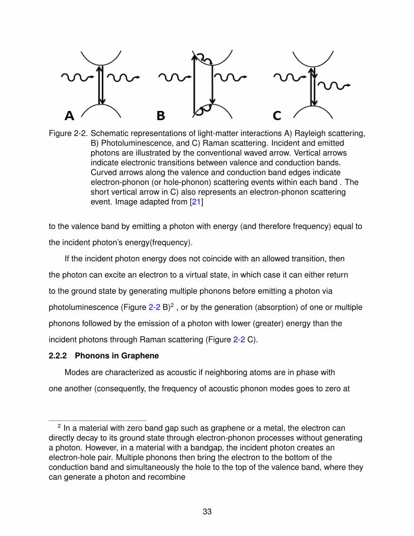
Figure 2-2. Schematic representations of light-matter interactions A) Rayleigh scattering,B) Photoluminescence, and C) Raman scattering. Incident and emittedphotons are illustrated by the conventional waved arrow. Vertical arrowsindicate electronic transitions between valence and conduction bands.Curved arrows along the valence and conduction band edges indicateelectron-phonon (or hole-phonon) scattering events within each band . Theshort vertical arrow in C) also represents an electron-phonon scatteringevent. Image adapted from [21]
to the valence band by emitting a photon with energy (and therefore frequency) equal to
the incident photon’s energy(frequency).
If the incident photon energy does not coincide with an allowed transition, then
the photon can excite an electron to a virtual state, in which case it can either return
to the ground state by generating multiple phonons before emitting a photon via
photoluminescence (Figure 2-2 B)2 , or by the generation (absorption) of one or multiple
phonons followed by the emission of a photon with lower (greater) energy than the
incident photons through Raman scattering (Figure 2-2 C).
2.2.2 Phonons in Graphene
Modes are characterized as acoustic if neighboring atoms are in phase with
one another (consequently, the frequency of acoustic phonon modes goes to zero at
2 In a material with zero band gap such as graphene or a metal, the electron candirectly decay to its ground state through electron-phonon processes without generatinga photon. However, in a material with a bandgap, the incident photon creates anelectron-hole pair. Multiple phonons then bring the electron to the bottom of theconduction band and simultaneously the hole to the top of the valence band, where theycan generate a photon and recombine
33

the zone center), and are optical if neighboring atoms are out of phase(resulting in
non-zero frequency at the zone center). Acoustic modes are so-named because of their
relation to sound waves in the long wavelength limit, while the term optical refers to the
sensitivity of the these phonon modes to electromagnetic radiation which allows them to
be probed by optical methods.
Modes are further categorized as either longitudinal if the vibrational amplitude
of the phonon mode is parallel to the wave propagation direction, or transverse if the
amplitude is perpendicular to the propagation direction.
As described in Section 1.3, graphene has a two atom basis3 , and therefore has
six characteristic phonon branches: two in-plane optical branches, one longitudinal
(iLO) and one transverse(iTO); one out-of-plane transverse optical branch (oTO); and
two in-plane acoustic branches, one longitudinal (iLA) and one transverse(iTA); one
out-of-plane transverse optical branch (oTA).
Near the � point, the six eigenvectors of graphene’s normal modes correspond to
three translational modes (acoustic) and three vibrational modes (optical). At this point,
all three acoustic phonon modes have zero frequency, while the iTO and iLO modes are
degenerate, and the remaining oTO mode remains non-degenerate.
At the K and K ′ points, the iTO phonon mode is non-degenerate while the iLO and
iLA branches are degenerate.
2.2.3 The Graphene Raman Spectrum
2.2.3.1 Characteristic Peaks
Raman spectroscopy takes advantage of the difference in energy between incident
and emitted photons, by relating the frequency shift to the phonon modes of a material.
The phonon modes are directly representative of the symmetry properties of a material,
thus can be used to determine its chemical and structural properties.
3 A two-atom basis in 3 dimensions gives rise to six degrees of freedom
34

Figure 2-3. Graphene Phonons. A) Phonon dispersion relation of graphene. B)Illustration of real-space atomic motion corresponding to normal vibrationalmodes. Letters above each image indicate whether the mode is associatedwith the � point or the K point, followed by the abbreviation describing thetype of phonon mode and the corresponding Group Theory notation. Figuretaken from [21].
The prominent features in the graphene Raman spectrum include the G-peak
located at ∼ 1580 cm−1, the 2D peak4 at ∼ 2700 cm−1, and the D peak at ∼ 1350 cm−1
(Figure 2-6).
The G peak, located at ∼ 1580 cm−1, is due to inelastic scattering involving the
doubly degenerate iTO and iLO phonon modes (E2g symmetry in group theory notation)
at the � point of graphene’s Brillouin zone and is associated with the stretching of
in-plane stretching of C-C bonds in sp2 bonded carbon systems. It is the only peak
resulting from a one-phonon, or first order, Raman scattering process.
4 The name ”2D” is a bit of a misnomer in that this peak arises from a doubleresonance process and is not in fact an overtone of the D peak, despite its position atapproximately twice the frequency of the D peak. This peak is sometimes referred to asthe G′ peak instead in the literature.
35

Figure 2-4. Schematic representation of the scattering processes corresponding to theG peak and the 2D peak. Electron(solid circle)-hole(open circle) pairs arecreated with the absorption of an incident photon. Solid arrows representinelastic scattering due to phonon generation and absorption.
An electron, initially in a state i with energy Ei , is excited to a state A in the
conduction band by a photon with energy EA − Ei , at the same time generating a
hole in the valence band. It is then scattered by a phonon with q ≈ 0, where q describes
the phonon wavevector, to a state B with energy EB . The electron can then return to its
original state by emitting a phonon with energy EB −Ef . Conservation of energy requires
Ef = Ei .
Using Fermi’s golden rule, we may estimate the maximum intensity of the Raman
signal for the one phonon resonance process:
I ∝∑f
∣∣∣∑A
MfBMBAMAi
(Ei − EA − iγA/2)
∣∣∣2 (2–1)
where MAi = ⟨c , k |He−light |v , k⟩ is the matrix element describing the interaction
between the incident light and the electron in its initial state ,|v , k⟩, in the valence band
with wavevector, k which excites the electron to a virtual state A; MBA = ⟨c , k +
q|He−phonon|c , k⟩ describes the electron-phonon interaction which leaves the electron
in a state B, still in the conduction band;(Remember here that q = 0 for the first order
process) MfB = ⟨v , k |He−light |v , k + q⟩ describes the interaction with the emitted photon,
which returns the system to its initial state in the valence band with wavevector,k . γA
describes the line-width of the peak and is related to the inverse of the excited state
36

lifetime. He−light and He−phonon represent the interaction Hamiltonians for electrons with
the incident photons (He−light) and with the generated phonons (He−phonon).
The 2D peak, located at ∼ 2700 cm−1 (Figure 2-6) in the graphene Raman
spectrum, arises from a higher order resonance process involving inelastic scattering by
two iTO phonons near the K and K′ points of the graphene BZ.
In this process, an electron, initially in a state i with energy Ei , is excited to a state
with EA by a photon with energy EA − Ei , just as in the one-phonon case described
above. However, in the double resonance case, the requirement for a near zero phonon
momentum is relaxed [22]. Instead, momentum can be conserved by only requiring∑n qn = 0. From the excited state A(|c , k⟩) with initial momentum k , an electron
can be inelastically scattered by an iTO phonon with q = 0 near the K point to a
state(|c , k + q⟩) with wavevector k + q near the K′ point with energy EB . A second
inelastic scattering event with an iTO phonon with −q will return the electron to a state
C with energy EC that returns the electron to its original momentum value near the K
point (|c , k + q − q⟩ = |c , k⟩). Finally, the electron returns to its original state (|v , k⟩)
where it can recombine with a hole, emitting a photon with energy EC −Ei (|v , k⟩). For the
two-phonon resonance process, the intensity is given by:
Iα∑f
∣∣∣ ∑A,B,C
MfCMCBMBAMAi
(Ei − EC − iγC/2)(Ei − EB − iγB/2)(Ei − EA − iγA/2)
∣∣∣2 (2–2)
where MAi = ⟨c , k |He−light |v , k⟩ and MfC = ⟨v , k |He−light |c , k⟩ describe the absorption
and emission of the photon respectively, while MBA = ⟨c , k + q|He−phonon|c , k⟩ and
MCB = ⟨c , (k + q) − q|He−phonon|c , k + q⟩ = ⟨c , k |He−phonon|c , k + q⟩ represent the
two electron-phonon interactions described above. γA, γB , and γC are the inverse of the
lifetimes of the electronic excitations of the virtual states A, B, and C respectively.
A triple resonance process, in which an electron generated near the K point with
wavevector k is scattered to a state with wavevector k + q near the K ′ point while at the
37

Figure 2-5. Schematic representation of the double resonant Raman scatteringprocesses responsible for the D and D′ peaks, and the triple resonantprocess contributing to the 2D peak. The D peak is an intervalley processinvolving both an elastic and an inelastic scattering event. The D′ peak is anintravalley process also involving both elastic and inelastic scattering events.The triple resonance process involved which contributes to the 2D peak isalso shown.
same time a hole generated with wavevector k near the K point is scattered by a phonon
with k − q so that the electron and hole recombine near the K′ point, also contributes to
the intensity of the 2D peak.
The 2D peak is of particular importance, due to its sensitivity to the amount of order
in a graphitic system. Because the double (and triple) resonance phenomena require
scattering off two separate points in the BZ, they require a higher degree of symmetry in
the system than is required for the first order resonance peak.
The Raman features near 1360 cm−1 and 1620 cm−1 are closely related to the
amount of disorder in the system and is therefore known as the D peak (Figure 2-6).
Both the D peak, located near 1360 cm−1, and the D′ peak, located near 1620 cm−1
originate from a double resonance process involving elastic scattering off a defect site,
and inelastic scattering through the generation/absorption of an optical phonon. The two
processes are distinct from one another in that the D peak involves an iTO phonon and
scattering between K and K′ points (intervalley scattering), whereas the D′ peak involves
an iLO phonon and scattering around the same K (or K′ point) (intravalley scattering)
[23].
38

Figure 2-6. Raman spectra of graphene and graphene related materials are shown.From top to bottom spectra are shown for: graphene, highly oriented pyroliticgraphite (HOPG), single wall carbon nanotubes (SWNT), damagedgraphene, and amorphous carbon. This image has been adapted from [21]
Generally speaking, we may conclude that if the G band is present in the Raman
spectrum, there must be some sort of sp2 bonding present in the system. The presence
of the D band indicates disorder in the system; it is not present in highly ordered
systems such as HOPG and mechanically exfoliated graphene. The presence of the
2D band indicates a greater degree of order in the system; it is not present in highly
disordered systems such as amorphous carbon or glassy carbons [24]
2.2.3.2 Relative Peak Intensities
The Raman spectrum is plotted as the intensity versus frequency shift, where the
intensity is given in arbitrary units. This means that the absolute intensity of each peak is
unimportant; it can be easily affected by slight changes in the orientation or roughness
of the sample surface. What really matters is the relative intensity of the peaks with
respect to one another. The relative intensity of the D peak (ID) compared to the G peak
intensity (IG ), written as ID/IG , is an indicator of the degree of disorder in the system.
39

Tuinstra and Koenig, through performing a systematic analysis of Raman spectra from
graphitic samples of varying quality, determined that the graphene crystallite size (La)
was inversely proportional to the ID/IG ratio.[25] Later, Knight and White proposed an
empirical formula to determine the actual value of La from ID/IG by observing the Raman
spectra of graphitic systems measured using a λ = 514.5 nm laser. Cancado et al. later
expanded this to a more general equation that can be used for any choice of incident
laser light. [26]:
La(nm) = (2.4× 10⁻¹⁰)λ4l( IDIG
)−1 (2–3)
The I2D/IG ratio is crucial in identifying single layer graphene samples. The Raman
spectrum of monolayer graphene ideally has an I2D/IG ratio of ∼ 2 − 6, while multilayer
graphene and graphite present with I2D/IG < 1. This difference can be attributed
to electronic band splitting in MLG systems due to Bernal stacking (ABAB), which
breaks the symmetry of the A and B sublattices. The Raman scattering processes
are illustrated in Figure 2-7 . Electronic band splitting in bilayer graphene gives rise to
4 parabolic bands[27], therefore allowing additional phonon transitions between the
bands, splitting the 2D peak into 4 components, thus diminishing the intensity of each
component. Additionally, third order scattering events are suppressed [22].
2.2.4 Determining One Allotrope From Another
The Raman signals from numerous carbon allotropes is shown in Figure 2-6. The
graphene spectrum is shown first, with characteristic G and 2D (labeled as G′ in the
figure) peaks. The HOPG signal differs from the graphene signal in the height and
shape of the 2D peak. In the case of graphene the 2D peak intensity is typically four
times larger than the G peak. In bulk graphite samples, this peak is diminished to an
intensity lower than the G peak. Moreover the shape of the 2D peak is different in
graphene and HOPG samples, exhibiting a sharp single-Lorentzian peak for graphene,
while consisting of two or more components for a multilayer sample.
40

Figure 2-7. The second order Raman scattering process. A) Monolayer graphene. B)Bilayer graphene. Electronic band-splitting in bilayer graphene activateadditional phonon modes through intervalley transitions labeled asq1A, q1B , q2A, and q2B .Image from [28]
Single-Wall Carbon Nanotubes (SWCNT) display a similar Raman signal, but
with the addition of a radial breathing mode (RBM) with a low frequency Raman shift.
Additionally large strains and confinement effects result in a splitting of the G peak into
G− and G+ components.
The Raman spectrum of damaged graphene is shown next. In this spectrum,
symmetry breaking due to defects in the crystal lattice activate additional vibrational
modes due to a combination of elastic and inelastic scattering events. Overtones of
these modes (G”) and combinations with ideal modes (D+G) can also be present.
Lastly, the amorphous carbon spectrum is shown. Broad peaks vaguely resembling
D and G bands are clear, but the 2D peak is conspicuously absent in these samples.
41

CHAPTER 3STABLE HOLE DOPING OF GRAPHENE FOR LOW ELECTRICAL RESISTANCE AND
HIGH OPTICAL TRANSPARENCY
3.1 Electron and Hole Doping in Semiconducting Materials
Doping is a method used in the semiconductor industry for decades in which the
electrical properties of a material can be changed by introducing additional charge
carriers to the system.1 If electrons are added to a host material’s conduction band,
it is said to be n-doped. While if holes are added to its valence band, it becomes
p-doped. Figure 3-1 shows the energy band structure of a p-type material produced
through substitutional doping. In the figure, foreign atoms added to a sample provide
an available energy level within the band-gap of the pristine material that can accept
electrons from the valence band, leaving behind positively charged holes. For an n-type
material, an energy level near the sample’s conduction band can donate electrons to the
system. n- and p- type doping can be accomplished in a number of ways:
• substitutional doping
• surface charge transfer
• electrical gating
Each of these approaches has advantages and disadvantages. In the first
technique, substitutional doping, atoms in the original crystal lattice are replaced
with dopant atoms that donate either holes or electrons to the system. Typically this is
accomplished by either introducing dopant gases while the sample is annealed at high
temperatures or through ion implantation. The former method has been successfully
implemented to produce n-doped graphene by annealing samples in an ammonia (NH4)
1 Excerpts from Tongay, S., et al. ”Stable hole doping of graphene for low electricalresistance and high optical transparency.” Nanotechnology 22.42 (2011): 425701 andfrom Miao, X., et al. ”High efficiency graphene solar cells by chemical doping.” Nanoletters 12.6 (2012): 2745-2750 have been reprinted with permission in this chapter.
42

Figure 3-1. Energy band structure after conventional doping. Electrons have beenaccepted into the donor material from the semiconductor.
environment. [29] Exposure to dopant atoms at high temperatures allows those atoms to
become permanently bonded into the material. This provides excellent stability, but also
creates defect sites within the lattice, impeding charge carrier mobility in substitutionally
doped materials. The latter method, ion implantation, cannot be applied to monolayer
graphene samples as the energetic ions will puncture the graphene layer, passing
through it to the underlying substrate.
Surface charge transfer (Figure 3-2), on the other hand, is a technique applied
post-growth whereby charges separate at the interface between a sample and a dopant
material. The advantage of this method is that though the dopant material is in contact
with the sample, it does not change the sample’s lattice structure, and so does not
directly add defects to the sample. However, charged impurities at the surface of either
the dopant material or the underlying substrate can still affect the sample’s mobility by
introducing charge scattering sites very near to the doped region.
Electrical gating can also be used to modify a sample’s charge carrier concentration.
Most commonly, this is achieved in graphene systems through back-gating a heavily
doped Si substrate separated from the graphene by a 300nm silicon oxide layer. By
adjusting the applied bias, the graphene Fermi level can be tuned as desired to produce
43

Figure 3-2. Energy band structure before and after surface charge transfer doping. (a)Upon contact of a surface doping material with the material to be doped, and(b) after electrons have been transfered from the target material to thedopant (acceptor), thereby introducing holes near the surface of the targetmaterial.
either n- or p-doped graphene. Though this method provides the finest control out of the
three methods, it requires a constant applied voltage often a large as hundreds of volts
to achieve and maintain the desired doping levels. Once the bias is removed, the system
returns to its pre-doped2 state.
3.2 Hole Doping Graphene with TFSA for Optoelectronic Applications
This section describes a method for p doping of graphene by modifying the surface
with bis(trifluoromethanesulfonyl)amide, TFSA ([CF3SO2]2NH). The electrical and optical
properties of TFSA/graphene at temperatures from 300 K down to 5 K and fields from
0 to 7 T are discussed. It was found that the graphene sheet resistance decreases by
70% while the optical transparency decreases by only 3% after doping. The sheet
resistance of graphene initially exhibiting high values has been reduced through
2 A distinction must be made between the pre-doped or ]pristine state and an un-doped state as many methods of graphene synthesis produce unintentionally dopedsamples. For example, CVD graphene is almost always p-doped during the transferprocess
44

doping to values reaching as low as 129 , which is comparable to the resistance of
150-300 A thick indium tin oxide (ITO) thin films. Electrical properties of TFSA/graphene
remain unchanged over time in the atmosphere, displaying superior environmental
stability owing to TFSA’s hydrophobic character. Electrical transport measurements
support increased hole carrier density in graphene after charge transfer. Within the
Drude formula, the increase in nh is accompanied by a slight decrease in mobility µ
that results in an overall increase in the conductivity. The effect of TFSA doping on the
carrier density of graphene was confirmed by Raman spectroscopy measurements.
The increase in the peak position of the G and 2D peaks and a decrease in the 2D to G
peak intensity ratio (I2D/IG ) imply that graphene becomes hole doped after interacting
with TFSA. The intensity of the D peak remains unchanged after doping, meaning that
the doping process does not induce additional defects in the system. Moreover, TFSA
doped graphene displays excellent optical transparency in the visible and near-infrared
spectrum where ITO and fluorine-tin oxide (FTO) thin films strongly absorb light in the
near infrared (NIR) range. Our results demonstrate reproducible modulation of EgrapheneF ,
enhanced conductivity with environmental stability and an almost negligible change in
the optical transparency of graphene.
3.3 Experimental Details
Large area graphene sheets were synthesized on 25 µm thick copper foils using
a multi-step, low pressure chemical vapor deposition (CVD) process [30]. After the
graphene growth, 1 µm thick poly(methyl methacrylate) (PMMA) (11% in anisole) was
spin-cast on one side of the Cu foils at 2500 rpm for 2 min and post-baked at 125◦C
for 3 min, allowing the PMMA to harden. Prior to the Cu etching step, the backsides of
the Cu foils were etched in O2 plasma for 15 s to remove the unwanted graphene. Cu
films were then etched in a 0.05 mg L−1 solution of Fe(III)NO3 for 12 h to remove the
copper foils. The PMMA supported graphene films were then washed in deionized water
45

Figure 3-3. Sample geometry and undoped Raman spectra. A) Undoped graphenesheets were transferred onto SiO2/Si or sapphire substrates and were incontact with Au/Cr contact pads improving electrical contact. B) Aftertransfer, graphene was doped by applying TFSA in solution to the samplesurface. Inset, molecular formula of TFSA. C) Raman spectra taken ongraphene transferred onto SiO2/Si and sapphire substrates
multiple times to remove contaminants absorbed on the graphene surface during etching
and dried using N2 gas.
Prior to graphene transfer, Au/Cr (50nm/1 nm) contact pads were evaporated in a
six terminal configuration (Figure 3-3) onto SiO2/Si substrates by thermal evaporation
at 8 ×10⁻⁷ Torr pressure. While the gold (Au) pads allow good electrical contact to the
graphene sheets, the contact configuration in Figure 3-3 allows us to measure the sheet
resistance, Hall voltage, and number of carriers in graphene. Graphene sheets were
then transferred onto electrical contact pads, SiO2 and sapphire substrates by applying
a drop of isopropyl alcohol (IPA) onto the substrates and placing PMMA-graphene on
top. After the transfer, the PMMA thin films were dissolved in an acetone vapor bath
overnight followed by acetone and IPA baths. The transferred graphene sheetes were
identified/characterized using a Horiba-Yvon micro-Raman spectrometer with a green
(532 nm) laser.
The organic dopant, TFSA, was dissolved in nitromethane (20 mM) and spin-cast
onto transferred graphene sheets at 1200-2500 rpm for 1 min. Surfaces were analyzed
46

Figure 3-4. Scanning electron microscope (SEM) images. A) graphene sheets grownonto copper foils B) Graphene sheets modified by spin-casting TFSA at 800rpm, C) 1100 rpm, D) 1700 rpm, and E) 2500 rpm. Scales are indicated ineach image respectively.
by scanning electron microscopy (SEM) (Figure 3-4 A-E) and Raman spectroscopy
(Figure 3-6). Electrical properties of the pristine and TFSA modified graphene were
measured in a six terminal contact configuration from 300 K down to 5 K and from 0 to 7
T magnetic field range. Optical spectra of the quartz, TFSA/quartz, graphene/quartz and
TFSA/graphene/quartz were measured in the visible and near-infrared range (Figure
3-7) using a Zeiss microscope photometer with zenon and tungsten lamps as a light
source.
3.4 Results and Discussion
3.4.1 Reduced Resistivity and Environmental Stability
Polymers, atoms and gases absorbed on graphene are prone to desorption and
therefore chemically doped graphene has previously been found to degrade over time
[31]. We avoid degradation of electrical properties by using TFSA; hydrophobic TFSA
is an excellent candidate for doping graphene for long term environmental stability.
Electrical properties of transferred large area graphene sheets were measured on seven
47

different samples with graphene sheet resistance values (Rgraphene) ranging from 0.5
to 5.0 k. This wide range of Rgraphene values can be attributed to slight differences in
growth parameters as well as induced defects/disorder during the transfer process.
Figure 3-5 A illustrates the change in Rgraphene with respect to time prior ro and after
surface modification with TFSA. Upon TFSA doping, Rgraphene consistently decreases
by ∼ 70 ± 2% for all the samples measured, achieving a minimum value of 129 in
a sample which originally measured 425 before doping. To this end, our preliminary
results show that while the doping time (the total time required to spin TFSA onto the
graphene sheets) does not significantly change the doping level, increasing the TFSA
concentration up to 20 mM allows on to control (increase) the doping level, and thus
the conductivity of the sample. Increasing the TFSA concentration beyond 20mM no
longer affects sample conductivity. The improvement in graphene’s sheet conductivity
can be attributed to the electron-acceptor nature of TFSA, inducing hole carriers after
adhering to the graphene surface. We note that the Rdopedgraphene values depend on the
initial value of each graphene sheet’s resistance, Rgraphene , implying that the initial value
of graphene’s EF as well as density of disorder deterines the final value of the sheet
resistance. Interestingly, the electrical properties of our doped graphene samples are
well preserved with only a minuscule increase(∼ 2.8±0.5%) in Rdopedgraphene after one month
exposure to atmosphere.
Even though the decrease in Rgraphene is mostly attributed to the increase in the
carrier density nh, within the Drude formula (σgraphene = nheµ), the electrical conductivity
of graphene depends on the carrier density and mobility µ. To determine the individual
effects of changes in nh and µ on the electrical conductivity of the graphene, we
measure carrier density at room temperature before and after soping. Hall resistance
(Rxy versus magnetic field data taken before doping (Figure 3-5 C, red squares) imply
that transferred samples are doped with hole carrier densities of nh ∼ 1.9×1013cm−2. We
note that the initial carrier concentration is higher than the values expected for exfoliated
48

Figure 3-5. Electrical measurements taken before and after doping with TFSA. A)Change in sheet resistance before and after doping with time. The regionmarked in red indicates when the graphene sheets were doped. B)Temperature dependence of the graphene sheet resistance before and afterdoping. C) Hall resistance (Rxy ) data. D) Magnetoresistance data taken ondoped and undoped graphene sheets at room temperature.
graphene. These values can be attributed to impurities induced at the graphene surface
by the chemicals, such as acetone and Fe(III)NO3, used to etch Cu foils to release
the graphene sheets and to transfer them to various substrates such as sapphire and
SiO2/Si. The hole carrier density nh increases by 5.2 times to nh ∼ 9.9 × 1013cm−2
after doping (Figure 3-5 C, blue squares). Using the Drude formula in combination
with the factor of 3.3 increase in conductivity (corresponding to the 70% decrease in
R), we conclude that the increase in nh is compensated by a decrease in mobility to
63% of the original value. In addition, since the Fermi energy in graphene changes as
EF (n) = ~|vF |√nπ, such increases in nh decrease (increase) the E
grapheneF (Wgraphene , work
function of graphene) by ∼0.7 eV due to the acceptor nature of the TFSA polymer.
3.4.2 Effects on Carrier Mobility
The mobility of the graphene depends on various factors such as graphene growth
parameters, density of disorder [30], number of carriers [32] and coupling of graphene to
49

the substrate. In our measurements, µ was determined from data taken before and after
doping with TFSA on the same graphene sheet, thus changes in mobility can only be
attributed to doping, independent of variations in the growth parameters used. Moreover,
according to Raman spectroscopy measurements, the D peak intensity, associated
with the density of disorder in the system, remains unchanged before and after doping,
implying that the doping process does not induce additional defects.
So far, a number of scattering processes affecting the carrier mobility in graphene
have been proposed and are under active debate. It has been previously reported that
graphene’s mobility is limited mainly due to short range scattering [33], carrier scattering
off of the charged impurities [34], and surface optical phonons of SiO2 (or any dielectric)
[35]. Here, charged impurities are assumed to be either on the graphene sheet or at the
graphene/substrate interface and they interact with graphene by a Coulomb potential
which is inversely proportional to the permittivity of the medium. After transferring
graphene onto SiO2, the average permittivity of the medium (ϵaverage) can be estimated
as ϵair + ϵSiO2, and doping graphene with TFSA increases ϵaverage to ϵair + ϵSiO2
. While the
increase in ϵaverage weakens the Coulomb scattering by charged impurities (and therefore
increases µ), charge transfer between TFSA and graphene enhances the charged
impurity scattering, leading to overall reduction in µ. Moreover, scattering by thermally
excited surface phonons becomes comparable to scattering from charged impurities at
room temperature, and the use of an additional dielectric (TFSA) on the other side of the
graphene enhances the surface optical phonon scattering (due to increased ϵaverage) [36].
Despite the possible presence of alternative processes contributing to the reduction of
mobility in our system, we believe that it si predominantly the combination of these two
effects, i.e. charged impurity scattering and thermally excited surface phonon scattering,
that causes the overall reduction in µ, consistent with observed reduction in carrier
mobility in graphene at higher carrier density [32].
50

The aforementioned reduction in mobility (scattering time) to 63% of the original
value leads to a decrease in the magnitude of the magnetoresistance by a factor of
0.632 = 0.4, which typically scales as MR ∼ ωcτ)α where ωc is the cyclotron frequency,
τ is the scattering time [37, 38] and α is approximately 2, in qualitative agreement with
the curves shown in Figure 3-5 D. At the same time, an increase in nh manifests itself
in metallic-like temperature dependence of Rgraphene in Figure 3-5 B. Rgraphene remains
unchanged from 300 K down to 50 K, where Rgraphene starts increasing with decreasing
temperature. At temperatures T ≤ 50 K, σgraphene scales as σgrapheneαlnT , which is
indicative of quantum corrections (weak-localization effects) in two dimensions. Doped
graphene displays metallic-like behavior as temperature decreases until 20 K, i.e.
Rdopedgraphene decreases with decreasing temperature, at which point quantum corrections
begin to dominate, leading to a slight increase in sheet resistance below 20 K (Figure
3-5 B).
3.4.3 Raman Spectra Before and After Doping
After discussing the electrical properties of doped and undoped graphene, we
now consider the evolution of the Raman spectra by doping. Changes in the Raman
spectra of electrically biased graphene and doped graphene sheets with aromatic
molecules have been discussed previously, where it has been found that the G and
2D peak positions are sensitive to changes in the carrier density [39, 40], allowing
the determination of the nature of doping and corresponding changes in EF . Figure
3-6 A shows the Raman spectra taken at different spots on graphene/SiO2 and
graphene/sapphire samples in the 1200-3000 cm−1 range before and after doping.
Small D peak intensity and large 2D to G intensity ratio (I2D/IG ∼ 2.5) imply that
graphene sheets are single layer and are not significantly disordered. After doping
with TFSA, unlike with substitutional doping, the intensity of the D peak and hence the
density of disorder remain unchanged (Figure 3-6 A-C). Moreover, closer inspection
of the G (Figure 3-6 B) and 2D ( Figure 3-6 C) Raman peak shifts reveals significant
51

Figure 3-6. A) Raman spectrum taken at different spots on the graphene/sapphire (SiO2)samples before and after doping. B) Zoomed in Raman spectra ongraphene/SiO2 before (black line) and after (red line) doping. C) Zoomed inRaman spectra on graphene/sapphire before (green line) and after (blueline) doping.
changes in peak positions with doping: (1) the G (2D) peak starts at 1588 cm−1 (2676
cm−1) and increases up to 1611 ± 2 cm−1 (2692 ± 3 cm−1), and (2) I2D/IG decreases
from 2.0-2.5 to 0.7-1.0. We note that the TFSA doping brings the G peak position
closer to the D′ (disorder activated) peak located at 1620 ± cm−1. Since the D′ peak is
observable when the D peak intensity is much higher than the G and the 2D peak, we
do no expect to observe the D′ peak in our system and therefore shifting the G peak up
52

Figure 3-7. Transmittance versus wavelength taken on pristine quartz (black),graphene/quartz (red), TFSA/graphene/quartz (blue) and TFSA/quartz(green). A) The visible spectrum. B) The near-infrared spectrum.
to 1611 ± 2 cm−1 has no effect on our interpretations. These changes in the prominent
Raman features of graphene imply that, after doping, the graphene sheets are hole
doped and the change in EgrapheneF is of the order of 0.5-0.7 eV [41], consistent with our
electrical transport measurements, which predict 0.7 eV change in EgrapheneF (Figure 3-5).
3.4.4 Transmittance Before and After Doping
While TFSA modified graphene shows improved conductivity and superior
environmental stability, maintaining graphene’s high transparency is important
for integrating doped graphene sheets into light emitting devices and solar cells,
where harvesting or transmission of light through the graphene layer is critical.
Figure 3-7 shows the transmittance of quartz (black line), graphene/quartz (red line),
53
TFSA/graphene/quartz (blue line), and TFSA/quartz (green line) as a function of
wavelength in the 400-800 nm range. Quartz and TFSA/quartz substrates show 95%
and 92.8% transmittance respectively, independent of wavelength (λ). After transferring
graphene onto quartz substrates, the transmittance of graphene/quartz drops to 92% at
600 nm and the transmittance of graphene, as well as that of TFSA/graphene, becomes
a function of λ. Even though TFSA is optically transparent, charge transfer at the
TFSA/graphene interface dopes graphene and the increase in carrier density increases
(decreases) the overalll reflectance (transmittance) by ∼ 3% [42]. Above 800 nm, the
transmittance of TFSA/graphene increases monotonically and saturates at 92 ±1%
at 1500 nm (Figure 3-7 B), preserving graphene’s superior optical properties. More
interestingly, while TFSA/graphene possesses high transparency in the near-infrared
range with sheet resistance values comparable to those of 150-300 A thick ITO thin
films, ITO starts absorbing light above 1000 nm and its transparency decreases to
25% at 2000 nm. If the electrode can be made both transparent in the near-infrared
and conductive, then the light can propagate to the active layers of (a) narrow bandgap
based solar cells and (b) novel thermoelectric based cells, which use the Seebeck effect
to generate electricity. Therefore, unique optical properties of TFSA modified graphene
in the visible and near-infrared spectrum with improved conductivity make these films
ideal for various applications.
3.5 Conclusions and Applications
In summary, graphene sheets transferred onto various substrates were p-doped
with TFSA ((CF3SO2)2NH). Upon modifying graphene with TFSA, the sheet resistance
of the samples decreases by 70% of the original value, reaching 129 , and thus is
comparable to ITO and FTO values, while samples display superior environmental
stability and optical properties. The electrical properties of the doped graphene remain
relatively unchanged with time. We attribute the reduction in th sheet resistance to
the acceptor nature of the TFSA, increasing the hole carrier density in graphene by
54

5.2-fold as determined by Hall resistance measurements. Within the Drude formula,
the increase in hole carrier density is accompanied by a decrease in the mobility of
graphene (63% of the original value) but ultimately increases the conductivity of the
graphene sheets. Raman spectroscopy measurements performed on pristine and doped
graphene samples reveal significant shifts in G and 2D peak positions, implying that the
EF of graphene decreases by 0.5-0.7eV, consistent with the acceptor nature of TFSA
and the observed electrical transport properties, from which we have estimated a 0.7
eV decrease in EF TFSA doped graphene displays high transparency from 300-2500
nm, preserving graphene’s optical properties, and is superior to ITO films, where
transparency decreases to values of 30-40% in the near-infrared range. The presented
results allow us to fabricate environmentally stable graphene sheets with superior
electrical-optical properties, giving them a conspicuous advantage for implementation
in optoelectronic and solar cell devices and for tuning device characteristics at the
graphene/semiconductor interface.
In fact, TFSA doping has already been successfully integrated into graphene/n-type
Si solar cells [14, 43]. In these devices, it was demonstrated that TFSA treatment
could be used to increase solar cell power conversion efficiency (PCE). Single layer
graphene/n-Si Schottky junction solar cells under AM1.5 illumination exhibited PCE
values of 1.9% before and 8.6% after TFSA doping, increasing performance by a
factor of 4.5 to reach what was at the time the highest reported PCE values for any
graphene-based solar cell. For more information regarding specific measurements taken
to explore the mechanisms behind the increased efficiency upon doping, the reader may
refer to X. Miao’s dissertation[14].
55

CHAPTER 4CURRENT TRANSPORT ACROSS THE PENTACENE/CVD-GROWN GRAPHENE
INTERFACE FOR DIODE APPLICATIONS
4.1 Introduction
Organic semiconductors have recently attracted a great deal of interest due to
their low cost of fabrication and potential applications on flexible substrates. Pentacene
(C22H14), an organic molecule comprised of a string of five benzene rings, has become
predominant in the field due to its relatively high mobility (∼1 cm2/Vs) and has been
employed in various device geometries such as Field Effect Transistors(FETs) [44, 45],
Active Matrix Organic Light Emitting Diodes (AMOLEDs) [46–48], and photovoltaic (PV)
devices [49, 50].1 More recently, the molecular arrangement of pentacene grown onto
highly ordered pyrolytic graphite (HOPG) [51] and graphene [52] substrates has been
shown to be significantly different compared to the pentacene thin films grown on most
metals; the alignment between the π orbital of sp2 bonded carbon (C) in graphene (or
HOPG) and pentacene is optimized in such a way that pentacene molecules mostly
orient themselves parallel to the graphene (HOPG) surface (Figure 4-1) while pentacene
assumes a nearly vertical orientation when grown on most metals [53].
Parallel orientation of pentacene allows higher mobility perpendicular to the
substrate surface via coupling between the π-orbitals, and improved device operation in
vertically structured devices has already been displayed using pentacene on carbon
nanotubes in the vertical FET (VFET) configuration [54, 55]. However, despite
knowledge of the growth properties of pentacene molecules on these materials, the
electronic transport across pentacene/graphene (or HOPG) junctions has not been
investigated; these junctions are fundamentally interesting as they provide the building
1 Excerpts from Berke, K., et al. ”Current transport across the pentacene/CVD-growngraphene interface for diode applications.” Journal of Physics: Condensed Matter 24.25(2012): 255802 have been reprinted with permission in this chapter
56

Figure 4-1. Schematic diagram of Au/Pentacene/Graphene diodes. The inset figureillustrates the horizontal growth orientation of pentacene molecules on thegraphene surface.
blocks for future applications, i.e FETs, AMOLEDs, and PVs, where knowledge of
charge transport across the metal/semiconductor contacts is necessary.
In this article, we study the electrical properties of Au/pentacene/graphene,
Au/pentacene/HOPG, and Au/pentacene/Cu diodes using X-ray diffraction (XRD),
atomic force microscopy (AFM), current density (J) versus applied voltage (V )
measurements, and micro-Raman spectroscopy. We first consider the effects of
exposing our samples to air as environmental stability is necessary for many device
applications: In vacuum, diodes display poor rectification and upon exposure to the
atmosphere the forward current density (Jfor ) increases while the reverse current density
(Jrev ) decreases, resulting in marked improvement in the diode characteristics. Next,
we consider electrical characteristics of pentacene/graphene junctions and find that
pentacene/graphene diodes exhibit two distinct characteristics different from those
shown by pentacene/HOPG and pentacene/Cu junctions: (1) At low bias the charge
transport across the pentacene/graphene interface is dominated by Poole Frenkel
conduction, whereas pentacene/HOPG and pentacene/Cu transport is dominated by
thermionic emission and (2) the low density of electronic states around the Fermi level
(EF ) of graphene results in reduced rectification at the pentacene/graphene interface
through Schottky barrier height lowering with applied bias.
57

4.2 Experimental Details
Graphene sheets were first grown by chemical vapor deposition (CVD) onto 25 µm
thick copper foils using conventional CVD recipes [56]. After the growth, 1 µm thick
poly(methyl methacrylate) (PMMA) (11% Anisole) was spincast and hardened through
post-baking at 125 ◦C. The backside of the Cu samples was etched in O2 plasma to
remove unwanted graphene, then treated overnight in 0.05 mg/L Fe(NO3)3 solution to
remove the Cu foil leaving behind graphene sheets adhered to PMMA. After etching
the Cu foils, graphene/PMMA sheets were washed in deionized water repeatedly to
remove contaminants absorbed on the surface during the chemical etching step. HOPG
samples used in pentacene/HOPG junctions were cleaved from 0.5◦ mosaic-spread
samples to form 2 mm thick samples, which were then exfoliated to yield a flat surface
for pentacene deposition. To compare electrical properties of pentacene/graphene
and pentacene/HOPG junctions to those of typical pentacene/metal junctions, we have
prepared pentacene/Cu (25 µm thick Cu foils) diodes as well. Since the work function
of Cu (ϕCu ∼ 4.65 eV) is very similar to that of HOPG and graphene (ϕHOPG ∼ 4.6
eV), pentacene/Cu diodes are expected to yield similar Schottky barrier heights at the
interface, thus allowing us to distinguish differences between conventional metal- and
graphene-based pentacene diodes.
Pentacene (Aldrich 99%) films, 400 nm thick, were grown as supplied through
thermal vapor deposition from an effusion cell at 220 ◦C and pressures of 10−7 Torr
at a rate of 2 - 4 A/s onto graphene, HOPG, and Cu substrates. The growth direction
of pentacene was measured by X-ray diffraction (XRD) in the θ-2θ configuration and
confirmed by Atomic Force Microscopy(AFM).
After the pentacene deposition, diodes were transferred to a separate vapor
deposition chamber and 40 nm thick Au contacts were grown onto pentacene at a rate
of 2 A/s. Both deposition chambers were housed in a glovebox and kept in an argon
environment with an O2 concentration of less than 0.1 ppm. After fabrication, samples
58

were exposed to ambient atmosphere where current-voltage measurements were taken
with a Keithley 2400 sourcemeter immediately upon exposure to air and again after 24
hours, thus giving ample time for oxygen to diffuse throughout the sample [57].
J–V measurements were taken in the two-contact geometry as illustrated in Figure
4-1 where electrical contact was made between the top Au contact and the bottom
graphene, HOPG, or Cu electrode. In forward bias a positive voltage in the range 0 to
4 V was applied to the gold contact, which acts an ohmic contact to the pentacene. For
reverse bias measurements, voltages were swept from 0 to −7 V.
4.3 Results and Discussion
4.3.1 Pentacene Orientation
In Figure 4-2 A, we provide direct evidence that pentacene grows in a nearly vertical
orientation when deposited on Cu and mostly flat laying when deposited on HOPG and
graphene surfaces. While the XRD data taken on pentacene/Cu displays (001) and
related higher order peaks, implying that the pentacene orients in the vertical direction
consistent with previous studies [51, 58], data taken on pentacene/HOPG shows (022)
and (-210) peaks indicating a horizontal alignment. Considering the similarities between
the two sp2 bonded carbon allotropes, similar growth properties can be expected for
pentacene on graphene. However, our results reveal that pentacene grows mostly
parallel to the graphene surface ((022) and (-210)) but with some areas exhibiting
vertical growth (001). Such differences between pentacene growth on graphene and
HOPG might be associated with the quality of the graphene sheets including holes and
disorder in the graphene introduced through chemical processing.
AFM images confirm the differences in pentacene growth modes. Pentacene grown
on Cu yields large, regularly shaped grains in agreement with (001) growth [59, 60]
with an RMS roughness of 22.2 nm, whereas pentacene on HOPG exhibits smaller,
thinner grains with an RMS roughness of 14.2 nm. Pentacene on graphene yields a
combination of both growth modes: predominantly thin oblong grains with a few more
59

Figure 4-2. X-ray diffraction data and AFM images for pentacene on graphene, Cu, andHOPG. A) X-ray diffraction (XRD) data taken in the θ-2θ configuration onpentacene/graphene (top trace), pentacene/Cu (bottom trace), andpentacene/HOPG(middle trace). B) AFM image taken of pentacene/Cu. C)AFM images of pentacene/graphene. D) AFM image of pentacene/HOPG
regularly shaped areas and an RMS roughness of 25.1 nm. Together, AFM images
and XRD data confirm the nearly vertical growth of pentacene on Cu substrates, the
nearly flat orientation of molecules on HOPG, and a combination of growth patterns on
graphene.
4.3.2 Atmospheric Effects on Diode Performance
In Figure 4-3, we show J-V characteristics of pentacene on graphene, HOPG,
and Cu substrates immediately after exposing diodes to ambient air (blue triangles)
and after 24 hours(red squares). Additional measurements (not shown) were taken
after one week of exposure; electrical characteristics showed no change after the initial
24 hours, thus indicating full saturation of oxygen as well as environmental stability.
After saturation, all three types of diodes exhibit higher Schottky rectification ratios
60

with increased Jfor and decreased Jrev . During exposure, oxygen from the atmosphere
penetrates to all layers of the diode: i.e. the pentacene/bottom electrode interface,
the bulk pentacene, and the Au/pentacene interface. However, oxygen diffusion to the
pentacene/bottom electrode does not form an oxide on either graphene or HOPG,
while the oxide formed on copper substrates is sufficiently thin (previous studies have
shown copper oxides to be less than 5 nm thick even after 24 hours exposure to air [61])
to allow a high tunneling probability and thus still yields typical Schottky behavior
in agreement with previous studies on very thin oxide metal oxide semiconductor
devices [62, 63]. Additionally, oxygen can enter the bulk to hole-dope pentacene,
resulting in an increase in charge carriers that contributes to the increase in Jfor in all
three types of diodes as seen in Figure 4-3. Most significantly, oxygen penetrates to the
Au/pentacene interface and enhances the ohmic nature of the contact.
In vacuum, an interface dipole exists at the Au/pentacene interface resulting in
a discontinuity between the vacuum levels of these materials and thus creating an
initial Schottky barrier while samples are kept in vacuum [64]. This phenomenon arises
because unlike the band structure of conventional semiconductors and metals, organic
materials are characterized by molecular orbitals in which electrons are relatively
localized. Since electrons are not free to move throughout the organic material,
there is a high local electron density at the organic/metal interface that consequently
increases the Coulomb repulsion, suppressing the electron wavefunction from the
metal. This results in a discontinuity of vacuum levels between the two materials,
systematically decreasing the effective work function of the metal and resulting in an
initial barrier at the desired ohmic contact. The hole injection barrier at the Au/pentacene
interface is found to be lower after exposure to ambient air in agreement with previous
experiments [65, 66] in which passivation of an Au/organic interface leads to a reduced
barrier height. In fact, exposure to atmosphere nearly eliminates the barrier between
gold and pentacene, allowing the flow of holes from semiconductor to the metal.
61

Thus oxygen saturation at the Au/pentacene interface improves diode performance
by promoting hole injection from the gold contact, improving the ohmic nature of the
contact.
4.3.3 Current Transport Processes Across Rectifying Junctions
As discussed above, the ohmic contact in a Schottky diode is essential to making
electrical contact to the semiconductor, however transport across the pentacene/bottom
electrode interface is far more interesting as it is this interface that is responsible for the
rectifying behavior of the diode. We now turn our attention to the nature of the transport
across the pentacene/graphene /HOPG /Cu diodes after oxygen saturation(and thus a
satisfactory ohmic contact at the Au/pentacene interface) has been achieved.
Traditionally, metal/semiconductor contacts are described by the Schottky-Mott
model, in which an abrupt junction between the metal and semiconductor is assumed. In
the ideal limit, electronic transport across the interface can be described by thermionic
emission [67]]:
J = Js(T )[exp(qV
ηkBT)− 1] (4–1)
where Js=A∗T2exp[−qϕB/(kBT )] is the saturation current density, qϕB is the zero bias
Schottky barrier height (SBH) defined for a metal/organic p-type semiconductor interface
as the difference between the organic material’s highest occupied molecular orbital
(HOMO) level and the metal work function (ϕm), A∗ is the Richardson constant, T is the
absolute temperature, η is the ideality factor, and V is the applied voltage. An energy
level diagram for the pentacene/graphene interface using this model is shown in Figure
4-4 A.
According to Equation 4–1, J-V curves for Schottky diodes exhibit linear voltage
dependence when plotted on a semilogarithmic scale (lnJ-V ). Consistent with this
picture, pentacene/HOPG and pentacene/Cu diodes display adequate linearity in the
forward bias (in the 0 to 0.5 V range) (Figure 4-4 B), so that the ideality factor and
62
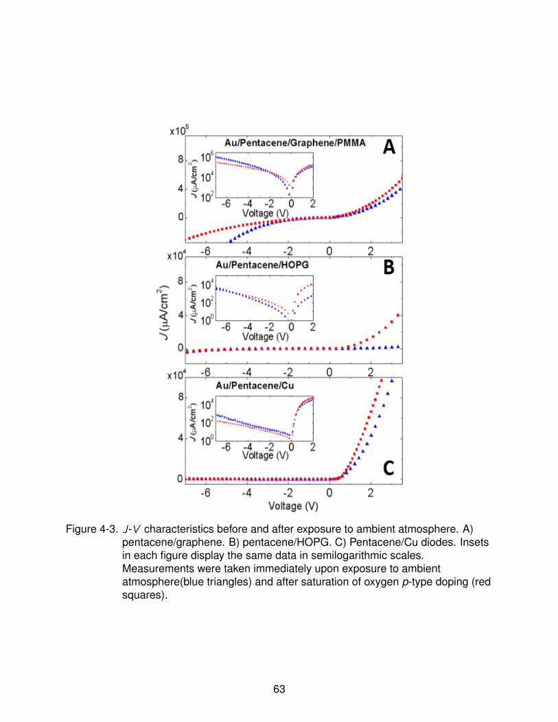
Figure 4-3. J-V characteristics before and after exposure to ambient atmosphere. A)pentacene/graphene. B) pentacene/HOPG. C) Pentacene/Cu diodes. Insetsin each figure display the same data in semilogarithmic scales.Measurements were taken immediately upon exposure to ambientatmosphere(blue triangles) and after saturation of oxygen p-type doping (redsquares).
63

the SBH can be extracted. In this voltage range, Schottky barrier heights of ∼0.49
eV and ∼0.52 eV for pentacene/HOPG and pentacene/Cu diodes respectively while
extracted ideality (η) varies from ∼2.5 for copper diodes to ∼3.0 for HOPG diodes. Upon
reaching a threshold voltage (∼ 0.5 V), the lnJ-V plots deviate from linearity, whereupon
calculated idealities exceed acceptable values (η >> 10) implying poor agreement with
the thermionic emission model.
Within the Schottky-Mott model, graphene is also expected to form a Schottky
barrier at the pentacene/graphene interface with similar electrical characteristics
to those observed for pentacene/HOPG diodes due to the similar workfunction
values and surface structures. Surprisingly, graphene/pentacene diodes’ electrical
characteristics differ significantly from those of HOPG and Cu based diodes: While the
pentacene/graphene diodes show rectification after atmospheric saturation (though to
a lesser extent than HOPG and Cu diodes), the absence of linearity in the graphene
lnJ-V plot suggests strong deviation from the conventional thermionic emission model.
The observed deviation from linearity can be attributed to (1) the existence of additional
current transport processes at the pentacene/graphene interface, which contribute to the
total current across the junction that overcomes the current due to thermionic emission
and (2) a low density of states around the Fermi energy(EF ) of graphene that results in a
voltage-dependent SBH.
4.3.3.1 Poole-Frenkel Conduction
We first turn our attention to the additional current processes at the pentacene/graphene
interface that result in deviation from thermionic emission theory. It has previously been
shown that for disordered and amorphous semiconductors, the thermionic emission
model fails due to the existence of trap centers in these materials, which lower the
effective barrier height by introducing bound states as described by the Poole-Frenkel
(PF) model [68, 69]. In this model, charge carriers need only a small activation energy
before they can tunnel to localized trap sites in the semiconductor. Trap sites act as
64
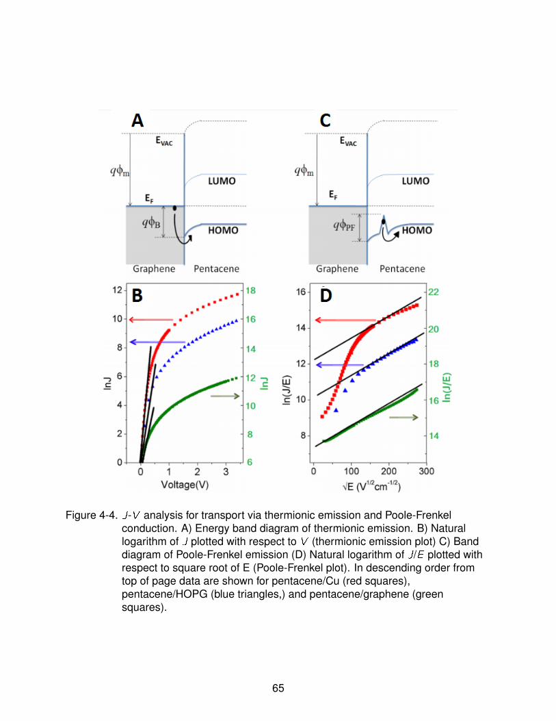
Figure 4-4. J-V analysis for transport via thermionic emission and Poole-Frenkelconduction. A) Energy band diagram of thermionic emission. B) Naturallogarithm of J plotted with respect to V (thermionic emission plot) C) Banddiagram of Poole-Frenkel emission (D) Natural logarithm of J/E plotted withrespect to square root of E (Poole-Frenkel plot). In descending order fromtop of page data are shown for pentacene/Cu (red squares),pentacene/HOPG (blue triangles,) and pentacene/graphene (greensquares).
65

potential wells from which charges can be removed by thermal activation. The energy
needed to remove an electron from a trap site is equal to the difference between the
SBH of the metal/semiconductor junction and the potential-well height of the trap [70]
as illustrated in the energy band diagram shown in Figure 4-4 C. The application of
an electric field can modify the potential barrier of the trap sites resulting in a field
dependent mobility: µ = µ0exp[−q(ϕPF − β√E)/(kBT )] [71] which can be applied to the
drift current equation, J = qnµE to yield the Poole-Frenkel current density [72]:
J = qnµ0E exp(−q(ϕPF − β
√E)
kBT) (4–2)
where q is the electron charge, n is the electron charge density, µ0 is the zero-field
electron mobility, E is the electric field extracted fromV/d where d is the thickness
of the deposited pentacene, and β = [q/(πϵϵ0)]1/2 where ϵ is the relative dielectric
constant of the material. According to Equation 4–2 if the current across the interface is
dominated by the PF process, plotting J-V in the ln(J/E ) versus√E form yields a linear
plot. The PF plots of ln(J/E ) versus√E for pentacene on graphene, HOPG and copper
substrates are illustrated in Figure 4-4 D. Here, we note that the pentacene/graphene
diodes show excellent linearity throughout the entire voltage range (0 to 4 V) while
pentacene/HOPG and pentacene/Cu diodes deviate from linearity at lower electrical
field values (corresponding to an applied bias of ∼0.5 V). Observed non-linearity at
low voltages in PF plots of pentacene/HOPG and pentacene/Cu is not surprising since
in this voltage range current processes are well described by thermionic emission as
evidenced by the observed linearity in the lnJ-V curves in Figure 4-3. However, as
forward bias approaches higher voltages, the ideality constant for both pentacene/HOPG
and pentacene/Cu diodes (obtained from Equation 4–1 ) reaches values well exceeding
η = 10, implying that the total current density across the junction cannot be expressed
by the thermionic emission theory alone; PF charge transport dominates the electric
transport at the junction under large applied biases.
66

As increased voltage is applied across the junction, there is a corresponding
decrease in the contact resistance across the barrier and the conduction becomes
bulk limited. Grain boundaries and other defects in the bulk crystal form trap centers
which become filled only at high fields as seen by the linearity of PF plots for all three
substrates above ∼0.5 V.
We see further evidence of PF conduction by looking at the PF slopes of the three
types of diodes, which determine the β value in the JPF . This value is directly affected
by the dielectric constant, which in an anisotropic molecule such as pentacene, is
found to have different values along the long and pi orbital axes[73]. We note that at
high voltages both pentacene/graphene and pentacene/HOPG exhibit a similar slope,
indicating that they exhibit similar molecular orientation. Pentacene/Cu diodes however
do not show the same PF slope, confirming that pentacene adopts a different orientation
when deposited on Cu.
The observed linearity in the ln(J/E ) versus√E curve for graphene/pentacene
diodes (green squares in Figure 4-4 D) across the entire voltage range implies that total
current density is described by the PF process even at low fields; whereas conduction
across the pentacene/HOPG (blue triangles) and pentacene/Cu (red squares) diodes
is predominantly characterized by thermionic emission at low electric fields and
becomes PF-like only at high fields. Here, we note that even though the orientation
of pentacene growth on both graphene and HOPG is similar, the electric transport at
the pentacene/bottom electrode junction differs dramatically. Therefore, we argue that
though we initially hypothesized that the orientation of pentacene growth would greatly
affect the charge transport across the pentacene/bottom electrode junction, it seems
that the orientation of pentacene molecules only affects the β value of the PF conduction
and does not control whether or PF conduction or thermionic emission is the dominant
current mechanism.
67
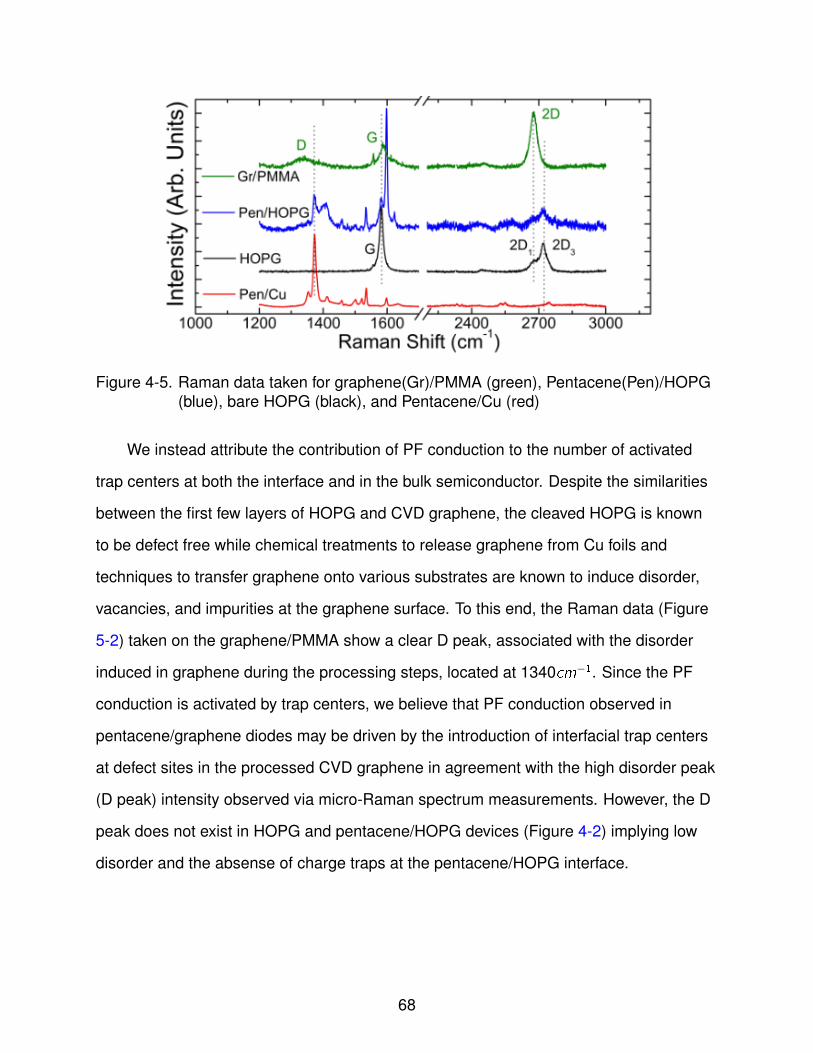
Figure 4-5. Raman data taken for graphene(Gr)/PMMA (green), Pentacene(Pen)/HOPG(blue), bare HOPG (black), and Pentacene/Cu (red)
We instead attribute the contribution of PF conduction to the number of activated
trap centers at both the interface and in the bulk semiconductor. Despite the similarities
between the first few layers of HOPG and CVD graphene, the cleaved HOPG is known
to be defect free while chemical treatments to release graphene from Cu foils and
techniques to transfer graphene onto various substrates are known to induce disorder,
vacancies, and impurities at the graphene surface. To this end, the Raman data (Figure
5-2) taken on the graphene/PMMA show a clear D peak, associated with the disorder
induced in graphene during the processing steps, located at 1340cm−1. Since the PF
conduction is activated by trap centers, we believe that PF conduction observed in
pentacene/graphene diodes may be driven by the introduction of interfacial trap centers
at defect sites in the processed CVD graphene in agreement with the high disorder peak
(D peak) intensity observed via micro-Raman spectrum measurements. However, the D
peak does not exist in HOPG and pentacene/HOPG devices (Figure 4-2) implying low
disorder and the absense of charge traps at the pentacene/HOPG interface.
68

4.3.3.2 Schottky Barrier Height Lowering in Graphene Diodes
In addition to the presence of interfacial trap centers, we attribute PF conduction
at low voltages in pentacene/graphene diodes to the inherently low density of states
in graphene, which under an applied voltage allows a dramatic change in the surface
charge density around EF , thus changing the graphene (and to a lesser extent HOPG)
work function. Hence, as voltage is applied to a graphitic material, the SBH becomes
a bias dependent quantity, unlike in conventional pentacene/metal diodes where an
applied voltage does not noticeably effect the EF of the metal due to a high density of
states.
This effect is observable for the pentacene/graphene diodes in reverse bias, where
thermionic emission logJ-V plots as seen in Figure 4-3 show an increase in Jrev with an
increase in applied bias, resulting in reduced rectification in agreement with previous
work on conventional semiconductor/graphene junctions [74, 75]. Similarly, diodes
fabricated on HOPG substrates, where the surface mimics that of a single sheet of
graphene (Bond polarization theory) [76, 77], also show increased Jrev with increased
bias in the reverse direction due to a lowered SBH. However, the effect is minimal in
HOPG diodes where rectification is orders of magnitude larger than for the graphene
diodes due to the slightly larger density of states in HOPG. In fact, SBH lowering is so
severe in graphene diodes that rectification is nearly eliminated, only reaching about 3
times rectification (where rectification is defined by the ratio JFor : JRev ), indicating that
the increased PF behavior of pentacene/graphene diodes at low voltages may be in part
due to a lowered contact resistance via a change in Fermi level with applied voltage. As
in the high voltage case, a lowered contact resistance would yield increased sensitivity
to bulk impedance caused by trapped charge centers in the bulk, leading to increased
PF currents.
69

4.4 Conclusions
Since the thermionic emission and Poole-Frenkel processes are simultaneously
occuring across the junction (depletion width of the diode), the conductivities are
additive. Using Equations 4–1 and 4–2, the total conductivity can therefore be written as:
Jtot = JPF + JTE
= γV
dexp(
qβ√
Vd)
kBT) + Js(T )[exp(
qV
ηkBT)− 1]
(4–3)
where the electric field E from Equation 4–2 in the PF term has been replaced by
V/d where d is the thickness of the semiconductor. The coefficient γ is a function of
the activated trap centers in the material. In the limit of zero interfacial trap centers
and initially zero charged trap centers in the bulk (γ∼ exp√ntrap[78] →0), the PF term
becomes negligibly small and the ideality constant approaches unity. In this limit, the
current density across the interface can be well described by Equation 4–1 and the
lnJ-V plots are linear [74].
As the applied voltage is increased, contact resistance at the interface decreases
and an increasing number of traps in the bulk pentacene become activated. Hence γ
increases with increasing voltage, ln(Jtotal ) is no longer directly proportional to V and
thermionic emission plots become nonlinear. Instead, as trap centers are filled in the
bulk, the number of accessible trap states becomes nonzero ((γ∼ exp√ntrap≫0) and
the JPF emission term overtakes the JTE term such that ln(J/E ) versus√E plots display
linearity (Figure 4-4 D).
For the case of pentacene/graphene diodes, trap centers at the graphene surface
also contribute to a nonzero γ even at low voltages. Additionally, the effects of SBH
lowering from a voltage-dependent EF yield an increased η value thus lowering the JTE
value. The contributions of these two factors to simultaneously raise both γ and η allows
the JPF term to dominate over the JTE term at low voltages and are responsible for the
70

striking linearity of the pentacene/graphene ln(J/E ) versus√E plot across the entire
voltage range.
In conclusion, we have studied the growth modes and electrical characteristics of
the pentacene/graphene interface and have drawn comparisons to transport observed
across pentacene/HOPG and pentacene/Cu junctions. We find similarity in the effects
of oxygen exposure to all three types of diodes through increased rectification (higher
Jfor and lower Jrev ) yielding stable characteristics after one day of exposure to ambient
atmosphere. After oxygen saturation, J-V characteristics of the pentacene/graphene
diodes differ significantly from those of pentacene/HOPG and pentacene/Cu diodes
despite pentacene exhibiting mostly similar growth patterns on graphene and HOPG
substrates. While the electric transport across the pentacene/HOPG(Cu) diodes can be
described by thermionic emission in low electric fields and Poole-Frenkel emission in
the high field limit, pentacene/graphene diodes can be described by the Poole-Frenkel
current mechanism in both low and high fields. We attribute these differences not
primarily to the orientation of pentacene molecules as predicted, but instead to the
enhancement of Poole-Frenkel emission in graphene diodes associated with the higher
disorder in CVD grown graphene which induces a higher density of trap centers in
pentacene, and to the reduction of thermionic emission through bias-induced Schottky
barrier height lowering due to the low density of states around the graphene Fermi level.
Study of the transport properties across the pentacene/graphene interface suggests
that rather than exhibiting large rectification, graphene provides a low resistance bottom
contact to pentacene. These results explain how vertically structured devices can still
take advantage of pentacene’s high mobility axis by orienting the majority of pentacene
molecules parallel to graphene’s surface, while at the same time reducing the resistivity
across the pentacene/graphene junction through enhanced PF emission and SBH
lowering. Consideration of current mechanisms across this interface is vital to the further
71

integration of these two prominent materials into device applications in the ever-growing
semiconductor industry.
72

CHAPTER 5ENHANCED GRAPHITIZATION OF SILICON CARBIDE THROUGH SURFACE ION
IMPLANTATION AND PULSED LASER ANNEALING
5.1 Introduction
Currently, the most common graphene growth processes include mechanical
exfoliation, chemical vapor deposition (CVD) onto copper or nickel foils, and epitaxial
growth on SiC substrates. Because mechanical exfoliation is a very low yield process,
it is not compatable with current industrial standards. CVD growth, on the other hand,
while capable of producing large-area graphene suitable for device fabrication, often
incurs significant damage to the graphene layer during transfer from the metallic foils
used to catalize growth to the insulating substrates required for devices. Additionally,
exposure to harsh chemical treatments during transfer and subsequent lithographic
patterning can lead to unintentional doping. Consequently, our most recent efforts have
been focused on developing industry appropriate methods for epitaxial graphene growth
on SiC–an insulating substrate–eliminating the need for transfer off of the orginal growth
medium. Additionally, we incorporate ion implantation (II) into our growth process, which
facilitates selective graphitic growth, only on the surface of implanted areas. This allows
for nanometer scale patterning of graphene through direct site-selective growth onto
insulating substrates without the need for potentially damaging lithographic treatments.
5.1.1 Epitaxial Graphene Growth on SiC
Previously epitaxial growth on SiC substrates has been accomplished through
thermally annealing SiC samples at high temperatures in ultra high vacuum (∼1200◦C[79])
or inert gas environments (∼1650◦C in Ar[80, 81]) for relatively long time periods
(typically ∼ 30 minutes[82]).
The two polytypes of SiC most often used for expitaxial graphene growth are
4H-SiC and 6H-SiC (Figure 5-1). Both of these structures are formed from stacks of
hexagonal bilayers. The unit cell for 4H-SiC consists of four such bilayers with ABCB
stacking, while the unit cell for 6H-SiC consists of six bilayers with ABCACB stacking.
73

Figure 5-1. Cross sectional view of 4H and 6H SiC structures. Samples can be cleavedto reveal Si-terminated (0001) (bottom), and a C-terminated (000�1) (top)surfaces.
In each arrangement samples may be cut to reveal both a Si-terminated (0001)
surface, and a C-terminated (000�1) surface, known as the Si-face and the C-face
respectively. Graphene can be grown on either face, but its structural and electronic
properties are different when grown on the Si-face when compared to the C-face.
Firstly, it has been found that under the same growth conditions, a greater number
of graphene layers forms on C-face than on the Si-face. This would seem to suggest
that for few layer graphene, the Si-face would prove more advantageous for growth.
However, the electronic properties of graphene grown on the C-face are actually
preferable for most graphene applications owing to electronic decoupling between
graphene layers grown on C-face SiC, which allows them to behave as monolayer
graphene [82].
74
Because of the difficulty in producing monolayer graphene on SiC through current
growth techniques, it is necessary to consider how graphene layers interact when
multiple layers are grown on the Si- and C- faces of 4H- and 6H- SiC.
5.1.1.1 Growth on the Si-Face
When graphene is formed on the Si face of 4H- and 6H-SiC, a layer of carbon
atoms, known as the 0-layer or buffer layer exists between the graphene sheets and
the SiC surface. Carbon atoms of this layer exhibit a hexagonal lattice with a lattice
constant approximately equal to that of monolayer graphene. ARPES measurements
in particular show graphene-like sigma bands, indicating C-C bond lengths in close
agreement to those found for monolayer graphene [80]. However, evidence of pi bands
is conspicuously absent from the data due to strong bonding between the buffer layer
and the underlying SiC substrate. As described in Chapter 1, graphene derives its
electronic properties from its π bands. Therefore, it is not surprising that the buffer layer
does not display the semi-metallic properties of monolayer graphene. The density of
atoms in the C buffer layer is approximately three times greater than the density of
Si atoms on the SiC(0001) surface, and so approximately one third of the C atoms
in the buffer layer interact with dangling bonds of the SiC(0001) surface [80]. Strong
bonding between the buffer layer and the underlying substrate results in nearly uniform
orientation of the first graphitic layer, and ABAB stacking of subsequent layers.
5.1.1.2 Growth on the C-Face
Meanwhile, using typical thermal annealing methods produces graphene directly on
the C-face after a series of SiC surface reconstructions, resulting in rotational disorder
even on the very first graphitic layer on the SiC surface. This rotational disorder persists
throughout multilayer samples and different rotation angles can even be found within
the same grain. Graphene grown on SiC manifests with two different orientations on the
SiC surface. The two orientations, as observed through LEED measurements taken by
a number of groups, are characterized by an angle ϕ between the graphene and SiC
75

lattice vectors. The first of these angles, ϕ = 30◦ is generally well established in the
literature, but controversy remains over the value of the second angle. Hass [82] et. al
argue ϕ2 = ± 2.2◦ (R2.2±) with regard to the underlying SiC, but Srivastava et. al [83]
argue that ϕ2 lies between 6 and 13◦, while Hiebel[84] reports ϕ2 = 14◦, and Hicks et.
al find [85] the ϕ = 0◦ ± 7◦. In any case, there exist two distinct orientations, indicating
only weak coupling between the first graphene layer and the substrate, in contrast to the
strong bonds between the 0-layer and the SiC substrate when graphene is grown on the
Si-face. The relatively weak bonds between layers in C-face grown graphene means that
these layers are electronically decoupled from one another. Prior research conducted
by Hass et al. indicates that the electronic decoupling between rotated graphene layers
as grown on the C-face of 4H-SiC reproduces the electronic structure of monolayer
graphene, even for samples tens of layers thick[16].
5.2 Site Selective Graphene Growth on SiC Using Ion Implantation
5.2.1 Previous Work
This work began as an extension of the work previously conducted at the University
of Florida by Tongay et al. [18] and Lemaitre et al.[17]. In their work, Tongay et al. began
with both 4H- and 6H-SiC substrates implanted with Au++ and Si++ ions at 30keV.
They found that the temperature necessary to produce graphene (i.e. the graphitization
temperature, TG ) was 100◦C lower for implanted SiC than for pristine SiC samples.
Thus, they were able to use ion implantation as a method to pre-pattern substrates prior
to thermal annealing. Then, by annealing these samples (in vacuum) to temperatures
above the TG for ion implanted SiC, but below the TG for pristine graphene, they were
able to selectively graphitize only the pre-patterned regions. Typically, epitaxial graphene
produced by thermally annealing SiC grows in such a way as to completely cover all
surfaces of a SiC substrate. After growth, photolithography, e-beam lithography, and
dry-etching (O2) techniques can be used to obtain patterned graphene [18]. However,
lithographic techniques often result in unintentional doping as a result of exposing
76

samples to various chemicals during processing; while dry-etching creates defects at
graphene edge sites. Selective graphitization as achieved by Tongay et. al through ion
implantation prior to thermal annealing eliminates the need to employ harsh lithographic
treatments.
Lemaitre et al.[17] similarly used ion implantation to pre-pattern substrates, but
instead of thermally annealing their samples, they used a pulsed excimer laser to
irradiate samples. Because conventional thermal annealing techniques require high
growth temperatures (∼1200◦C in UHV [79], ∼1650◦C in Ar[80, 81]) for relatively
long time periods (typically ∼ 30 minutes[82]),they are prohibitive to integration into
commercial production lines. Graphene synthesis through pulsed laser annealing
(PLA) SiC presents a promising alternative approach[18, 86, 87]. PLA is ideal for
integration into CMOS production as sample heating is localized to a few hundred
nanometers below the sample surface, allowing on-chip fabrication. Additionally, PLA
can be conducted rapidly in a variety of environments (including in air), therefore
eliminating inherent limits posed by vacuum or furnace parameters. Lemaitre et al.[17]
report producing multi-layer graphene on SiC samples through the PLA of SiC under
the following implant conditions: 60 keV Au at 3.6 ×10¹⁶ Au/cm2, 40keV Cu at 8.0
×1016 Cu/cm2, and 40keV Ge at 3.5 ×10¹⁶ Ge/cm2. Samples were annealed using a
193nm ArF laser with 25ns pulse duration at a repetition rate of 20Hz. Laser fluences
were varied over a range of 0.1-1.2 J/cm2 to determine the onset of graphitization in
samples as characterized by the relative intensity of D- G- and 2D- peaks present in the
Raman spectra obtained from each sample (Chapter 2.2 for details on the origin and
implications of the presence of these peaks).
Lemaitre et. al found that the laser fluence (power density) necessary to produce
graphene through the PLA of SiC substrates was lower in implanted regions than for
unimplanted regions. A number of mechanisms were proposed to account for the onset
of graphitization at lower fluences in implanted samples versus unimplanted samples.
77

At the time of their experiments, it was unclear whether enhanced graphitization was
due primarily to the presence of foreign ionic species (Au and Cu were thought to act as
catalysts to the graphene growth process, while Ge served as an isoelectronic additive)
after ion implantation, or to the changes in thermal properties of implanted substrates
from surface amorphization caused by the ion implantation process.
5.2.2 Growth in the Absence of Foreign Ionic Species
In this work, we demonstrate that surface amorphization alone, without the
presence of catalytic species, can be used with pulsed laser annealing (PLA) to create
site selective graphitization of 6H-SiC substrates. We accomplish this by implanting
6H-SiC samples with approximately equal doses of Si and C ions, which allows us
to amorphize the sample surface without introducing foreign ionic species, prior to
pulsed laser annealing. Samples were characterized by Raman spectroscopy, and
cross-sectional transmission electron microscopy (X-TEM).
For this report, the (000�1) face of commercially available 6H-SiC wafers were
implanted at the Australian National University with Si and C atoms to amorphize the
top 20 nm of the substrate surface, as measured by ion-scattering channeling using 2.0
MeV He+ ions at normal incidence with a 110◦ scattering angle and 20◦ exit relative to
the sample surface. Both implanted and unimplanted samples were annealed using a
JPSATM IX-260 ArF laser (193nm wavelength, 25 ns pulse width, 50 Hz repetition rate).
To optimize PLA parameters, the laser fluence was varied from 0.1-1.2 J/cm2 and the
number of pulses ranged from 1 to 2000 pulses.
Raman spectra were obtained using a Horiba-Yvon MicroRaman Spectrometer
with a 532 nm green laser before and after annealing samples at 0.8 J/cm2 for 2000
pulses (Figure 5-2). The spectra taken from the ion implanted samples before PLA
have a slightly enhanced peak at 1407 cm−1 owing to a small contribution from the
amorphous SiC Raman spectrum. After annealing, no significant contribution from the
original amorphous Raman spectrum was visible, implying either complete sublimation
78

Figure 5-2. Raman spectrum taken before and after pulsed laser anneals (PLA)implanted and unimplanted samples at 0.8 J/cm2 for 2000 pulses in Argon
of the layer or recrystallization. Previous studies on the thermal evaporation rate of
SiC during excimer pulsed laser annealing (PLA) at 1.2 J/cm2 in vacuum resulted
in the loss of ∼ 3 × 10⁻² monolayers/ pulse [88] Under equivalent conditions, a
maximum of 300 A of SiC could be evaporated in 2000 pulses, and therefore it would
be reasonable to assume complete evaporation of the Si from the amorphous SiC
layer on our samples. However, during PLA at 0.8 J/cm2, samples reach temperatures
above the Si sublimation temperature (∼1300K[89]), but below the amorphous SiC
melt temperature (∼2445K[90]). Rather than evaporating off a molten layer, Si may
preferentially sublimate from the solid surface while residual C atoms form graphitic
structures in a process similar to that described for graphene formation via thermal
annealing of SiC.
After annealing both implanted and unimplanted samples yielded Raman peaks at
1350 cm−1 and 1588 cm−1, corresponding to the D and G peaks of graphitic carbon’s
Raman spectra. A very slight increase in intensity near 2700 cm−1 corresponding to
graphitic carbon’s 2D peak is present in the unimplanted sample’s Raman spectrum
79

Figure 5-3. Raman spectra taken of implanted and unimplanted samples after PLA at0.8 J/cm2 for 2000 pulses in air, after subtraction of the SiC signal. Intensity(y-axis) is relative to the SiCTO peak located at 1520 cm−1 in Figure 5-2
after annealing, while a much more pronounced peak is present in the implanted
sample’s Raman spectrum.
The raw Raman spectra were then fit to a common baseline and normalized to the
crystalline SiC peak (SiCTO arising from an overtone of a transverse optical phonon
mode) located at 1520 cm−1. The relative intensity of the graphitic peaks with respect
to the SiC peak suggests that there is a greater amount of graphitic carbon in implanted
samples than in unimplanted samples after PLA. To evaluate the quality of graphitic
layers, the SiC signal was subtracted; from the resulting spectra (Figure 5-3, the
intensity of the graphitic peaks (IG , I2D , ID) was measured, yielding ratios of ID/IG = 1.5
and IG/I2D = 6.4 for unimplanted samples, and ID/IG = 1.9 and IG/I2D=2.0 for implanted
samples. An increase in the ID/IG ratio indicates increased scattering off defect sites in
implanted samples. However, a decreased IG/I2D ratio suggests either fewer graphene
layers[91] and/or decreased electronic coupling between graphene layers.[92]
Cross-sectional TEM (X-TEM) proved an essential complement to the Raman
analyses, owing to X-TEM’s unique ability to provide images of nanostructures, as well
80

Figure 5-4. Cross-sectional TEM (X-TEM) image of 6H-SiC, amorphized via ionimplantation to a depth of 20 nm, after pulse laser annealing at 0.8 J/cm2 for2000 pulses. Approximately 3 monolayers of epitaxial few-layergraphene(top) is observed adjacent to the 6H-SiC layer (bottom). Thedashed line indicates the interface between the sample surface and theprotective Cr layer.
as structural and compositional changes along the direction of heat flow in our samples.
Figure 5-4 shows an X-TEM image taken of an implanted sample. Approximately 3
graphene layers are observed directly adjacent to the 6H-SiC substrate, suggesting
epitaxial growth.
We attribute the presence of graphene (after PLA) only in implanted samples to
the differences in thermal properties of amorphous SiC from those of crystalline SiC.
Amorphous SiC and crystalline SiC have different absorption coefficients (α) , thermal
coefficients (κ) affecting heat transfer (the heat diffusion length is given by L =√Dτ ,
where D = κ/ρCp and τ is the pulse width of the laser) and therefore the time the
sample surface remains at elevated temperatures. We use the one dimensional heat
equation with a laser source term to approximate the surface temperature of implanted
versus unimplanted samples after exposure to one laser pulse (pulse width = 25 ns).
The one dimensional heat equation with a laser source term is given by [93]:
81

ρCp
∂T
∂t= αI (z , t) +
∂
∂z
(κ∂T
∂z
)(5–1)
where T represents the temperature of the sample, ρ the density, and Cp the specific
heat of the material. The intensity of light, I , is a function of both the time, t, after the
pulse begins and the depth, z , below the sample surface.
I (z , t) = I0(t)(1− R)exp(−αz) (5–2)
where I0 is the incident laser intensity at the sample surface and R is the reflectivity.
For simplicity, we assume a square wave laser pulse with fixed intensity, I0,
between t=0 and t=25 ns. Numerical solutions using the parameters listed in Table
5-1[90, 94, 95] result in an approximate surface temperature of ∼2100K for implanted
samples and ∼1680K for unimplanted samples after a single laser pulse at 0.8 J/cm2
from an ArF laser. Graphene grown on SiC via thermal annealing in Ar requires
growth temperatures near 1920K[80, 81], therefore it is not surprising that both the
quantity and the quality of graphene are higher in implanted samples which reach
temperatures in excess of 1920K after PLA at 0.8 J/cm2, than in unimplanted samples
which do not. Additionally, our calculations show that the surface temperatures of our
samples remained below the melting temperature of both amorphous (2445K) and
crystalline (3100K) SiC and, consequently, complications due to sample melting need
not be considered. Similar investigations on the affects of PLA on phase changes in
amorphous/crystalline SiC have shown that the minimum laser fluence needed to melt
the sample surface varies strongly with the thickness of the amorphous layer [90, 94, 95]
support our findings. Enhanced graphitization in implanted samples can therefore be
explained by an enhanced Si sublimation rate due to elevated temperatures that exceed
graphitization temperatures, but do not exceed melt temperatures, in ion implanted
amorphous/crystalline SiC samples.
82

Table 5-1. Parameters used in numerical analysis for SiC for both amorphous SiC(α-SiC) and crystalline SiC (c-SiC
Parameter α-SiC c-SiC
Density, ρ (g/cm3) 3.2 [94] 3.2 [94]Specific heat, Cp (J/g K) 1.3 [94] 1.3 [94]Thermal Conductivity, κ (W/cm K) 0.011 [94] 1.0 [94]Absorption Coefficient, α ( 106 cm−1) 1.1 [95] 1.5 [95]Reflectivity, R (%) 34.6 [95] 40 [95]Melting Point, Tm (K) 2445 [90] 3100 [96]
5.2.3 Conclusions
We have demonstrated that surface amorphization of crystalline SiC through
ion implantation, even in the absense of foreign ionic species, can result in selective
graphitization after pulsed laser annealing. We confirm the presence of graphene layers
through Raman spectroscopy and X-TEM images. Solutions to the one dimensional
heat equation reveal that ion implanted SiC reaches higher temperatures than
unimplanted SiC, but our samples do not reach melt temperatures.
The exact contributing mechanisms leading to the selective synthesis of graphene
are still under investigation. For the conditions reported here, Si sublimation seems
logical for temperatures below surface melting temperatures, and when appropriate
processing parameters are identified, it is possible to selectively synthesize epitaxial
graphene from thin amorphous surface layers on SiC. Our processing approach,
combining ion implantation and pulsed laser annealing for selective graphene growth
on 6H-SiC involves techniques more compatible with existing device manufacturing
techniques than conventional thermal annealing techniques; and sufficient flexibility
remains to improve and apply this approach to a range of problems.
5.3 Future Work: Optimizing Growth Parameters
While investigating the selective graphitization of SiC using ion implantation and
pulsed laser annealing, it became apparent that even a small change in amorphization
depth, laser fluence, the number of laser pulses, the environment in which samples were
83
annealed, and the type of ionic species implanted greatly affected sample morphology.
Each of these parameters can be the topic of further investigation.
5.3.1 Amorphization Depth
Originally, our work began with 6H-SiC samples that were implanted at selected
fluences and energies to produce 6 distinct amorphization depths dα: 0, 20 nm, 69.7
nm, 98.9 nm, 123.8 nm, and 216.7 nm as measured by ion-scattering channeling by our
collaborators at the Australian National University (Table 5-2)1 .
Table 5-2. Ion Implantation Conditions
Sample Si (1015 ions/cm2) Energy (keV) C (1015 ions/cm2) Energy (keV) dα (nm)
1 – – – – 02 1.5 10 1.75 4 203 1.5 40 1.5 18 69.74 1.5 60 1.5 27 98.95 1.5 80 1.5 37 123.86 1.8 160 1.8 75 216.7
Raman spectra were obtained from each of the samples after PLA at 0.8 J/cm2 for
100 pulses in air2 (Figure 5-5). All samples, with the exception of sample 1 (unimplanted
SiC, dα=0), displayed additional Raman peaks centered at 1580 cm−1, 2700 cm−1, and
1350 cm−1 corresponding to the G, 2D and D peaks of the graphitic Raman spectrum
respectively.
Despite enhancement in the relative intensity of the G peak to the SiCTO peak
(IG/ISiC ) with increasing dα (Figure 5-5 A, B), the ratio of the G to 2D peak intensities
(IG/I2D) remained fixed(in Figure 5-5 C spectra are renormalized to the G peak to
illustrate the relative intensity of peaks), suggesting that the concentration of graphitic
1 Special thanks to Dinesh K. Venkatachalam and Rob Elliman for their assistance inion implanting samples
2 Currently, samples annealed in argon at 0.8 J/cm2 for 2000 pulses are underinvestigation
84

Figure 5-5. Raman Spectra taken after PLA at 0.8 J/cm2 of samples 1-6. A) Spectrarescaled to the SiCTO peak at 1520 cm−1 B) Same spectra after subtractionof the crystalline SiC signal, resulting intensity represents the relativequantity of graphitic carbon in each sample C) Same spectra, renormalizedto the intensity of the graphitic G peak, located at 1580 cm−1, for visualinspection of ID/IG and IG/I2D
85

carbon near the sample surface increased with dα, while the concentration of defect
sites increased at the same rate; in other words, while the quantity of graphitic carbon
increased with dα, the quality of the resulting graphene remained the same, independent
of dα. However, at 100 pulses, the IG/I2D ratio of sample 2 is much larger than it was
after PLA in an argon environment with 2000 pulses (Figure 5-3). The reasons for this
discrepancy are unclear. Additional experiments for samples 3-6 after PLA in argon
for 2000 pulses are necessary to make direct comparisons to the results presented in
Section 5.2.2.
X-TEM images were obtained from sample 5 (Figure 5-6) after annealing at 0.8
J/cm2 for 100 pulses in air. Key differences are evident between graphitic growth
in samples 2 and 5. In sample 2 (Figure 5-4), few-layer graphene (FLG) is formed
directly adjacent to the 6H-SiC substrate, suggesting epitaxial growth. In contrast,
PLA of sample 5 resulted in the formation of a defected 3C-SiC region on top of the
crystalline 6H-SiC, and an amorphous region extending to the surface. FLG and carbon
nano-structures (CNS), sometimes called carbon onions, form at the surface on top of
the amorphous region. Additonal CNS are located in carbon-rich pockets in the 3C-SiC
layer.
The presence of CNS and a recrystallized 3C-SiC layer in sample 5, and their
conspicuous absence in sample 2 indicate different growth mechanisms in the two
samples. CNS are commonly reported following non-equilibrium processing (e.g. high
energy electron radiation [97], arc discharge [98], implantation into metals with low
carbon solubility prior to annealing [99]) of carbon-containing materials, but are not
typically observed after conventional thermal annealing of SiC. With this in mind, the
presence of CNS in sample 5 most likely indicates a non-equilibrium process, such
as laser-induced rapid melting of SiC, has occurred in contrast to the epitaxial growth
observed in sample 2, consistent with a solid phase transition. Thermal calculations
using Equation 5–1 estimate the surface temperature of sample 5 to exceed the melting
86

Figure 5-6. Cross-sectional TEM images taken of sample 5 (dα = 124nm) after pulselaser annealing at 0.8 J/cm2 for 100 pulses in air. A) shows the fullperspective indicating all the resulting structures: the 6H-SiC substrate(bottom left), followed by a 3C-SiC layer with increasingly large crystallitestructures, then an amorphous layer composed of both Si and C atoms, andfinally graphitic structures are present at the sample surface. Highermagnification images are shown of graphitic structures present at thesample surface including B) MLG layer and C) carbon onions. Additionalgraphitic ordering is present in the lighter shaded regions within the 3C-SiClayer D), presumably due to carbon nano-onions formed near the3C/amorphous carbon interface. The approximate position of the samplesurface is indicated by the white dashed line in each image.
87

Figure 5-7. Threshold fluences necessary to raise the surface temperature of a sampleduring a 25 ns pulse to the melting temperature of amorphous SiC, 2445K,versus amorphous layer thickness, dα, of amorphous/crystalline SiC.
temperature of amorphous SiC3 . Baeri et al. in similar investigations on the affects
of PLA (using a ruby laser) on phase changes in amorphous/crystalline SiC have
shown that the minimum laser fluence needed to melt the sample surface varies with
the thickness of the amorphous layer. Numerical simulations were conducted by
Dutto et al. [95]. and confirmed by Hedler et al. through additional calculations and
time-resolved reflectivity measurements[94]. Similarly, we construct a plot depicting
the threshold fluence required for the surface of amorphous/crystalline SiC to reach
the amorphous SiC melt temperature (2445K[90]) versus dα (Figure 5-7). According to
these calculations, one laser pulse at 0.8 J/cm2 will melt the sample surface in samples
3-6, whereas it is insufficient to melt samples 1 and 2. This may partially explain why
differences are observed between the type and location of graphitic structures found
in samples 2 and 5. In sample 2 the surface temperature stayed below the amorphous
3 current calculations do not include a moving melt front, and therefore additionalsimulations are necessary to estimate the temperature value
88
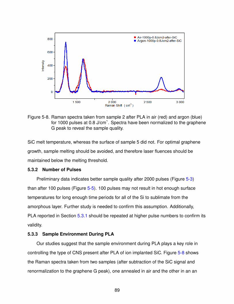
Figure 5-8. Raman spectra taken from sample 2 after PLA in air (red) and argon (blue)for 1000 pulses at 0.8 J/cm2. Spectra have been normalized to the grapheneG peak to reveal the sample quality.
SiC melt temperature, whereas the surface of sample 5 did not. For optimal graphene
growth, sample melting should be avoided, and therefore laser fluences should be
maintained below the melting threshold.
5.3.2 Number of Pulses
Preliminary data indicates better sample quality after 2000 pulses (Figure 5-3)
than after 100 pulses (Figure 5-5). 100 pulses may not result in hot enough surface
temperatures for long enough time periods for all of the Si to sublimate from the
amorphous layer. Further study is needed to confirm this assumption. Additionally,
PLA reported in Section 5.3.1 should be repeated at higher pulse numbers to confirm its
validity.
5.3.3 Sample Environment During PLA
Our studies suggest that the sample environment during PLA plays a key role in
controlling the type of CNS present after PLA of ion implanted SiC. Figure 5-8 shows
the Raman spectra taken from two samples (after subtraction of the SiC signal and
renormalization to the graphene G peak), one annealed in air and the other in an an
89
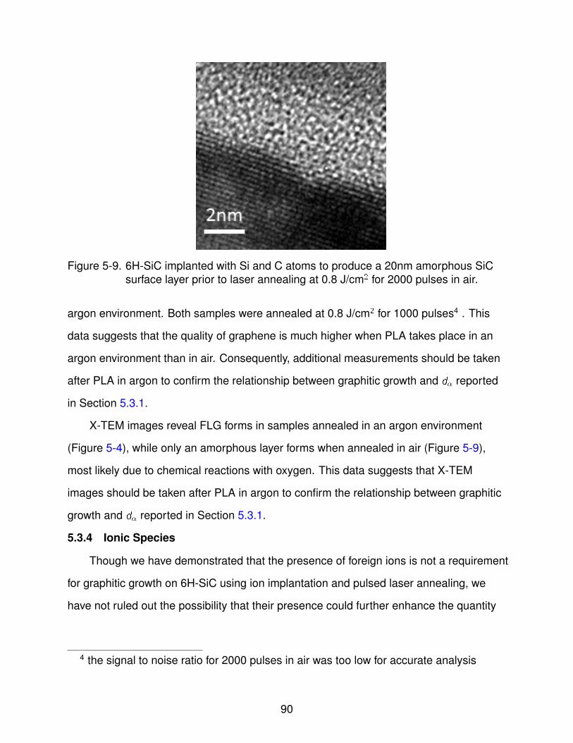
Figure 5-9. 6H-SiC implanted with Si and C atoms to produce a 20nm amorphous SiCsurface layer prior to laser annealing at 0.8 J/cm2 for 2000 pulses in air.
argon environment. Both samples were annealed at 0.8 J/cm2 for 1000 pulses4 . This
data suggests that the quality of graphene is much higher when PLA takes place in an
argon environment than in air. Consequently, additional measurements should be taken
after PLA in argon to confirm the relationship between graphitic growth and dα reported
in Section 5.3.1.
X-TEM images reveal FLG forms in samples annealed in an argon environment
(Figure 5-4), while only an amorphous layer forms when annealed in air (Figure 5-9),
most likely due to chemical reactions with oxygen. This data suggests that X-TEM
images should be taken after PLA in argon to confirm the relationship between graphitic
growth and dα reported in Section 5.3.1.
5.3.4 Ionic Species
Though we have demonstrated that the presence of foreign ions is not a requirement
for graphitic growth on 6H-SiC using ion implantation and pulsed laser annealing, we
have not ruled out the possibility that their presence could further enhance the quantity
4 the signal to noise ratio for 2000 pulses in air was too low for accurate analysis
90

Figure 5-10. Raman spectra taken after PLA at 0.8 J/cm2 for 2000 pulses in argon ofsample 2 in regions with and without additional Au+ implants. Top, rawspectra. Bottom, after subtraction of the crystalline SiC spectrum.
or quality of graphene produced during PLA. To this end, regions in sample 2 (dα =
20nm) were implanted with Au+ (5 ×10¹⁵Au+/cm2 at 30keV). We assume that the
surface of sample 2 was fully amorphized to a depth of 20nm; the addition of Au ions
into this depth cannot further amorphize the surface, and thus only results in the
introduction of a foreign ionic species without otherwise altering the thermal properties
of the sample. Raman data are shown in Figure 5-10. They suggest that both the
quantity (as measured by the relative intensity of graphitic peaks to the SiCTO peak at
1520 cm−1, Figure 5-10 lower panel) and the quality of graphene (as measured by the
(ID/IG)withoutAu ∼ 2 × (ID/IG)
withAu and (IG/I2D)withoutAu ∼ (IG/I2D)
withAu ratios) grown
91

after PLA are enhanced with the introduction of Au ions. Further experiments, in which
different types of ions (for example Cu or Ga ions) are implanted in a similar manner (by
implanting into already amorphized surface layers), may ellucidate the mechanisms for
the apparent enhancement in graphitization after the introduction of Au+ ions.
Though at this point there are still many parameters to investigate, through future
experiments into the affects of amorphization depth, laser fluence, the number of laser
pulses, annealing environment, and the type of ionic species implanted, we may gain
a clear understanding of the mechanisms behind graphene growth on 6H-SiC using
ion implantation and pulsed laser annealing. Ultimately, through optimizing these
parameters, we hope to achieve high quality, nano patterned graphene on insulating
substrates through direct epitaxial growth on SiC.
92

APPENDIX AGRAPHENE’S BAND STRUCTURE WITHIN THE TIGHT BINDING MODEL
R(A−B)1 =a√3x
R(A−B)2 =−a2√3x + a
2y
R(A−B)3 =−a2√3x − a
2
Step1: Construct Bloch states A, B using pz orbitals for the two sublattices A and
B:
�A =1√N
∑RA
ek·RAϕ(r − RA) (A–1)
�B =1√N
∑RB
ek·RBϕ(r − RB) (A–2)
Step 2: The Tight Binding Hamiltonian may be written as:
Htight−binding = Hatom + �U (A–3)
where Hatom is the unperturbed, well-localized atomic Hamiltonian, and �U is a small
perturbation accounting for the interaction between neighboring atoms. Inserting ⟨ϕpz ,A|
and ⟨ϕpz ,B | states into the Schrodinger equation, and considering only nearest-neighbor
interactions, we may write the secular equation for our system in terms of 2x2 matrices:HAA HBA
HBA HBB
= E
SAA SBA
SBA SBB
(A–4)
with elements:
HAA =1
N
∑RA
∑RA
e ik·(RA−RA)⟨ϕpz ,A(r − RA)|Hatom|ϕpz ,A(r − RA)⟩ = ϵpz (A–5)
93

HAB =1
N
∑RA
∑RB
e ik·(RB−RA)⟨ϕpz ,A(r − RA)|�U|ϕpz ,B(r − RB)⟩ (A–6)
= (e ik·R(A−B)1 + e ik·R(A−B)2 + e ik·R(A−B)3)⟨ϕpz ,A(r − RA)|�U|ϕpz ,B(r − RA − RA−Bj)⟩(A–7)
where in the last step, we choose to sum only over nearest neighbor atoms. We may
similarly determine the overlap integral components, Sm,n = ⟨�A|�B⟩, with sm,n =
⟨ϕA|ϕB⟩. We further define
f (k) = e ik·R(A−B)1 + e ik·R(A−B)2 + e ik·R(A−B)3 (A–8)
t = ⟨ϕA(r − RA)|�U|ϕB(r − RA − RA−Bj)⟩ (A–9)
so that we can concisely rewrite the Hamiltonian and resulting secular equation
ϵpz tf (k)
tf (k)∗ ϵpz
= E
1 sf (k)
sf (k)∗ 1
(A–10)
with solution:
E =ϵpz ± t
√|f (k)|2
1± s√
|f (k)|2(A–11)
When Si =j is set to 0, we arrive at:
E = ϵpz ± t
√1 + 4cos
√3kxa
2cos
kya
2+ 4cos2
kya
2(A–12)
94

APPENDIX BTHERMAL ANALYSIS OF PULSED LASER ANNEALING
In Chapter 5, the one dimensional heat equation with both a source term and a
phase change cannot be solved analytically. The governing differential equation is:
∂T
∂t=
α
ρCp
I (z , t) +1
ρCp
∂
∂z
(κ∂T
∂z
)(B–1)
where T is the temperature of the material, α is the light absorbtion coefficient, ρ is
the density, Cp the specific heat, and κ the thermal conductivity. I (z , t) describes the
intensity of laser light within the target material:
I (z , t) = I0(t)(1− R)e−αz (B–2)
where I0 is the intensity of the beam as it strikes the surface, and R is the reflectivity. If
α−1 << LD , where LD is the characteristic diffusion length LD = 2√Dt. with approximate
solution[100]:
T (z , t) =[2I√Dt
κ
]ierfc
[ z
2√Dt
](B–3)
rewriting ierfc(x) = (1/√π)exp(−x2)− x(1− erf (x))
T (z , t) =[2I√Dt
κ
] 1√πexp(−
[ z
2√Dt
]2)−
[ z
2√Dt
](1− erf (
[ z
2√Dt
])) (B–4)
At the surface (z=0):
T (0, t) =[2I√Dt
κ
] 1√π
(B–5)
Solving Equation B–5 with the parameters listed in table 5-1 for the minimum
fluence needed to arrive at the amorphous SiC melt temperature of Tm = 2445K [90],
the threshold fluence for melting amorphous SiC using one 25 ns pulse of an ArF is
0.116 J/cm2. Explicitly:
95

T (z = 0, t = 25ns) = 2445K =[2I0(1− 0.346)
√(0.002466cm2/s)(25× 10−9s)
0.011W /cmK
] 1√π
(B–6)
Similarly for crystalline SiC, where the melt temperature is Tm = 3100K , we obtain:
T (z = 0, t = 25ns) = 3100K =[2I0(1− 0.4)
√(0.2403cm2/s)(25× 10−9s)
1W /cmK
] 1√π
(B–7)
The minimum fluence necessary to raise the surface of crystalline SiC to its melting
temperature is then 1.48 J/cm2.
These values represent the minimum fluence required to bring a one-phase material
to the melt temperature, assuming a square wave laser pulse of constant intensity I0 is
applied to the surface. However, this type of solution is only applicable to a single phase
material. In our experiments, laser pulses were applied to crystalline materials, with
amorphous surface layers of varying thicknesses. Using the finite difference method,
and the parameters listed in Table 5-1, Equation 5–1 can be solved to determine the
threshold fluences required to raise the surface temperature of these layered materials
to the melting temperature.
We first establish a fixed grid in z and t. Assume we start with a substrate of length
Zmax , and then divide this substrate into j layers of length Zmax/j = �z . If we know the
temperature value T in each layer at some time t, then we can approximate the value at
a later time t+�t by rewriting the derivatives in Equation 5–1 as finite differences. There
are three common ways to approximate first derivatives:
1. forward differences
�+Tn = Tn+1 − Tn (B–8)
�2+Tn = = Tn+2 − 2Tn+1 + Tn (B–9)
96

2. central differences
�Tn = (Tn+1 − Tn−1)/2 (B–10)
�2Tn = �Tn+1 − 2Tn + Tn−1 (B–11)
3. backwards differences
�Tn = Tn − Tn−1 (B–12)
�2−Tn = Tn − 2Tn−1 + Tn−2 (B–13)
By combining methods 1 and 2, we obtain the Forward Time Central Space (FTCS)
model, so that Equation B–1 may be written:
�Tj ,k = Tj ,k+1 − Tj ,k = �t[ α
ρCp
I (z , t) +κ
ρCp
(Tj+1,k − 2Tj ,k + Tj−1,k
�z2
)](B–14)
where j indicates the jth spatial layer and k indicates the kth time step. However, many
of the coefficients used in this equation depend upon the phase of the material. For
example, the thermal conductivity of crystalline SiC is almost two orders of magnitude
larger than the thermal conductivity of amorphous SiC. Thus we must make the
distinction by writing:
�Tj ,k = Tj ,k+1−Tj ,k = �t[ α
ρCp
I (z , t)+1
ρCp
(κ+
Tj+1,k − Tj ,k
�z2+κ−
Tj−1,k − Tj ,k
�z2
)](B–15)
where the thermal conductivity terms, κ− representing the thermal conductivity between
spatial layers j and j+1, and κ+ representing the thermal conductivity between spatial
layers j and j+1, are determined by [101]:
2
κ±=
1
κj+
1
κj±1(B–16)
97

We may account for the difference in laser absorption coefficients by following the
method laid out by Ong et al. [101], where we define I1 and Ij>1:
I1 = I0(1− R1)1− exp(−α1�z)
α1�z(B–17)
Ij>1 = Ij−1exp(−αj−1�z) (B–18)
Note that in this method, only the reflectivity value of the surface material is considered
because in Ra ∼ Rc .1 Incorporating this into the full equation yields:
�Tj ,k =�t
ρc
[ In[1− exp(−αn)]
�z+ κ+
Tj+1,k − Tj ,k
�z2+ κ−
Tj−1,k − Tj ,k
�z2
](B–19)
The stability condition for the use of the FTCS method requires:
�t <�z2
4D(B–20)
In other words, the time step used for this method must be smaller than the heat
diffusion length (LD = 2√Dt) in order for the solution to be convergent for a given �z.
The algorithm used to compute T(z,t) proceeds as follows:
1. Divide the total thickness of the sample into j layers, each with a thickness of �z .
2. Construct a list containing the temperature Tj of each layer. At t=0 assume alllayers are at T=300K
3. Determine the relevant parameters:
• The phase of layer j at time k�t and the corresponding αj ,Rj , andκj values forthat phase
• The phase of layer j+1 at time k�t and the corresponding αj+1,Rj+1, andκ+values for that phase
1 This is not the case for the 3 phase system that includes a liquid SiC layer as wouldbe present during sample melting.
98

• The phase of layer j-1 at time k�t and the corresponding αj−1,Rj−1, andκ−values for that phase
4. Using Equation B–19 compute the temperature values of each spatial layer.
5. Step k → k+1.
6. Repeat from step 3 until k�t = 25 ns.
99

REFERENCES
[1] K. S. Novoselov, et al., Science 306, 666 (2004).
[2] K. Bolotin, et al., Solid State Communications 146, 351 (2008).
[3] C. Lee, X. Wei, J. W. Kysar, J. Hone, science 321, 385 (2008).
[4] A. A. Balandin, et al., Nano Letters 8, 902 (2008). PMID: 18284217.
[5] P. Wallace, Physical Review 71, 622 (1947).
[6] L. LD, II. Phys Z. Sowjetunion 11, 26 (1937).
[7] R. Peierls, Annales de l’institut Henri Poincare (Presses universitaires de France,1935), vol. 5, pp. 177–222.
[8] K. S. Novoselov, et al., Science 306, 666 (2004).
[9] L. Landau, Course of Theoretical Physics 5 (1958).
[10] N. D. Mermin, Physical Review 176, 250 (1968).
[11] J. C. Meyer, et al., Nature 446, 60 (2007).
[12] D. R. Nelson, T. Piran, S. Weinberg, Statistical mechanics of membranes andsurfaces, vol. 5 (World Scientific, 2004).
[13] A. Fasolino, J. Los, M. I. Katsnelson, Nature Materials 6, 858 (2007).
[14] X. Miao, Fundamental Studies of Graphene/Graphite and Graphene BasedSchottky Photovoltaic Devices (2013).
[15] X. Li, W. Cai, L. Colombo, R. S. Ruoff, Nano letters 9, 4268 (2009).
[16] J. Hass, et al., Physical Review Letters 100, 125504 (2008).
[17] M. G. Lemaitre, et al., Applied Physics Letters 100, 193105 (2012).
[18] M. G. Lemaitre, et al., Applied Physics Letters 100, 193105 (2012).
[19] X. Li, et al., Science 324, 1312 (2009).
[20] D. Abergel, A. Russell, V. I. Falko, Applied Physics Letters 91, 063125 (2007).
[21] A. Jorio, M. S. Dresselhaus, R. Saito, G. Dresselhaus, Raman spectroscopy ingraphene related systems (Wiley. com, 2010).
[22] L. Malard, M. Pimenta, G. Dresselhaus, M. Dresselhaus, Physics Reports 473, 51(2009).
[23] M. Pimenta, et al., Physical Chemistry Chemical Physics 9, 1276 (2007).
100

[24] A. Ferrari, J. Robertson, Physical review B 61, 14095 (2000).
[25] F. Tuinstra, J. L. Koenig, The Journal of Chemical Physics 53, 1126 (1970).
[26] L. Cancado, et al., Applied physics letters 88, 163106 (2006).
[27] A. Ferrari, J. Robertson, Physical review B 61, 14095 (2000).
[28] A. Ferrari, et al., Physical review letters 97, 187401 (2006).
[29] X. Wang, et al., Science 324, 768 (2009).
[30] X. Li, et al., Nano letters 10, 4328 (2010).
[31] H. Liu, Y. Liu, D. Zhu, Journal of Materials Chemistry 21, 3335 (2011).
[32] W. Zhu, V. Perebeinos, M. Freitag, P. Avouris, Phys. Rev. B 80, 235402 (2009).
[33] E. H. Hwang, S. Adam, S. Das Sarma, Phys. Rev. Lett. 98, 186806 (2007).
[34] A. Tsuneya, Journal of the Physical Society of Japan 75, 074716 (2006).
[35] S. Fratini, F. Guinea, Phys. Rev. B 77, 195415 (2008).
[36] A. Konar, T. Fang, D. Jena, Phys. Rev. B 82, 115452 (2010).
[37] A. B. Pippard, Magentoresistance in Metals, vol. 2 (Cambridge University Press,1989).
[38] Z.-M. Liao, Y.-B. Zhou, H.-C. Wu, B.-H. Han, D.-P. Yu, EPL (Europhysics Letters)94, 57004 (2011).
[39] A. Das, et al., Nature nanotechnology 3, 210 (2008).
[40] X. Dong, et al., Small 5, 1422 (2009).
[41] A. Das, et al., Nature nanotechnology 3, 210 (2008).
[42] L. Falkovsky, Journal of Physics: Conference Series (IOP Publishing, 2008), vol.129, p. 012004.
[43] X. Miao, et al., Nano letters 12, 2745 (2012).
[44] Y.-Y. Lin, D. Gundlach, S. Nelson, T. Jackson, Electron Device Letters, IEEE 18,606 (1997).
[45] C. D. Dimitrakopoulos, P. R. Malenfant, Advanced Materials 14, 99 (2002).
[46] L. Zhou, et al., Applied Physics Letters 88, 083502 (2006).
[47] T. W. Kelley, et al., Chemistry of Materials 16, 4413 (2004).
[48] I. Yagi, et al., Journal of the Society for Information Display 16, 15 (2008).
101

[49] S. Yoo, B. Domercq, B. Kippelen, Applied Physics Letters 85, 5427 (2004).
[50] A. C. Mayer, M. T. Lloyd, D. J. Herman, T. G. Kasen, G. G. Malliaras, Appliedphysics letters 85, 6272 (2004).
[51] J. Gotzen, D. Kafer, C. Woll, G. Witte, Physical Review B 81, 085440 (2010).
[52] W. H. Lee, et al., Journal of the American Chemical Society 133, 4447 (2011).
[53] M. Oehzelt, R. Resel, C. Suess, R. Friedlein, W. R. Salaneck, The Journal ofchemical physics 124, 054711 (2006).
[54] M. A. McCarthy, B. Liu, A. G. Rinzler, Nano letters 10, 3467 (2010).
[55] M. McCarthy, et al., Science 332, 570 (2011).
[56] X. Li, et al., Nano letters 10, 4328 (2010).
[57] O. D. Jurchescu, J. Baas, T. Palstra, Applied Physics Letters 87, 052102 (2005).
[58] M. A. McCarthy, et al., ACS nano 5, 291 (2010).
[59] M. Tejima, K. Kita, K. Kyuno, A. Toriumi, Applied physics letters 85, 3746 (2004).
[60] W.-S. Hu, Y.-T. Tao, Y.-F. Chen, C.-S. Chang, Applied Physics Letters 93, 053304(2008).
[61] J. Iijima, et al., Applied Surface Science 253, 2825 (2006).
[62] H. Card, E. Rhoderick, Journal of Physics D: Applied Physics 4, 1602 (1971).
[63] R. Singh, M. Green, K. Rajkanan, Solar Cells 3, 95 (1981).
[64] A. Kahn, N. Koch, W. Gao, Journal of Polymer Science Part B: Polymer Physics41, 2529 (2003).
[65] J. Hwang, A. Wan, A. Kahn, Materials Science and Engineering: R: Reports 64, 1(2009).
[66] A. Wan, J. Hwang, F. Amy, A. Kahn, Organic Electronics 6, 47 (2005).
[67] C.-T. Sah, Fundamentals of solid state electronics. (World Scientific, 1991).
[68] J. Frenkel, Physical Review 54, 647 (1938).
[69] R. M. Hill, Philosophical magazine 23, 59 (1971).
[70] D. S. Jeong, C. S. Hwang, Journal of applied physics 98, 113701 (2005).
[71] G. Horowitz, et al., Advanced Materials 10, 365 (1998).
[72] W. Gill, Journal of Applied Physics 43, 5033 (1972).
102

[73] E. V. Tsiper, Z. G. Soos, Physical Review B 68, 085301 (2003).
[74] S. Tongay, et al., Physical Review X 2, 011002 (2012).
[75] S. Tongay, et al., Applied Physics Letters 99, 102102 (2011).
[76] S. Tongay, T. Schumann, A. Hebard, Applied Physics Letters 95, 222103 (2009).
[77] R. T. Tung, Materials Science and Engineering: R: Reports 35, 1 (2001).
[78] L. Schein, A. Peled, D. Glatz, Journal of Applied Physics 66, 686 (1989).
[79] C. Berger, et al., The Journal of Physical Chemistry B 108, 19912 (2004).
[80] K. V. Emtsev, et al., Nature materials 8, 203 (2009).
[81] M. Ostler, F. Speck, M. Gick, T. Seyller, physica status solidi (b) 247, 2924 (2010).
[82] J. Hass, et al., Applied Physics Letters 89, 143106 (2006).
[83] P. Fisher, et al., Applied Physics Letters 95, 073101 (2009).
[84] F. Hiebel, P. Mallet, F. Varchon, L. Magaud, J. Veuillen, Physical Review B 78,153412 (2008).
[85] J. Hicks, K. Shepperd, F. Wang, E. Conrad, Journal of Physics D: Applied Physics45, 154002 (2012).
[86] C. Lee, X. Wei, J. W. Kysar, J. Hone, Science 321, 385 (2008).
[87] E. Hwang, S. Adam, S. D. Sarma, Physical review letters 98, 186806 (2007).
[88] R. Reitano, P. Baeri, N. Marino, Applied surface science 96, 302 (1996).
[89] A. Pimpinelli, I. Elkinani, A. Karma, C. Misbah, J. Villain, Journal of Physics:Condensed Matter 6, 2661 (1994).
[90] P. Baeri, C. Spinella, R. Reitano, International journal of thermophysics 20, 1211(1999).
[91] D. Graf, et al., Nano letters 7, 238 (2007).
[92] J. Hass, et al., Applied Physics Letters 89, 143106 (2006).
[93] H. S. Carslaw, J. C. Jaeger, Operational methods in applied mathematics (DoverNew York, 1963).
[94] A. Hedler, S. Urban, F. Falk, H. Hobert, W. Wesch, Applied Surface Science 205,240 (2003).
[95] C. Dutto, E. Fogarassy, D. Mathiot, Applied surface science 184, 362 (2001).
103

[96] R. Scace, G. Slack, The journal of chemical physics 30, 1551 (1959).
[97] D. Ugarte, Chemical physics letters 207, 473 (1993).
[98] N. Sano, et al., Journal of Applied Physics 92, 2783 (2002).
[99] T. Cabioc’h, J. Riviere, J. Delafond, Journal of materials science 30, 4787 (1995).
[100] J. Poate, Laser annealing of semiconductors (Access Online via Elsevier, 1982).
[101] C. Ong, H. Tan, E. Sin, Materials Science and Engineering 79, 79 (1986).
104
BIOGRAPHICAL SKETCH
Kara Berke was born in Lewisville, TX in 1986 to Richard and Sheryl Berke. She
was the second of three children. At the age of seven, she moved to Columbia, MD,
where she lived until 2005, when she graduated from Wilde Lake High School. During
high school, she was introduced not only to physics classes, but to the physics lab as
well. She began working two days a week with Ms. Ann M. Garrison Darrin at the Johns
Hopkins University Applied Physics Laboratory, working with micro electromechanical
systems. Though she started her undergraduate studies at Carnegie Mellon University
in mechanical engineering, she soon switched to physics, earning her B.S. in physics
in 2009. After fours years in the cold, overcast city of Pittsburgh, PA, she decided to
seek warmer climates, moving to Gainesville, FL in 2009 to begin her graduate studies
in the Department of Physics at the University of Florida. In the summer of 2010 she
joined Prof. Arthur Hebard’s research group. She earned her Ph. D in condensed matter
physics, specializing in graphene research, from the University of Florida in the fall of
2013.
105