graphics cards and graphics processing unitsmeseec.ce.rit.edu/551-projects/fall2011/2-2.pdf ·...
TRANSCRIPT
Ben Johnstone
Russ Martin
November 15, 2011
Graphics Cards and Graphics Processing Units
ContentsGraphics Processing Units (GPUs)
Graphics Pipeline
Architectures8800-GTX200
Fermi
Cayman
Performance Analysis
Conclusion
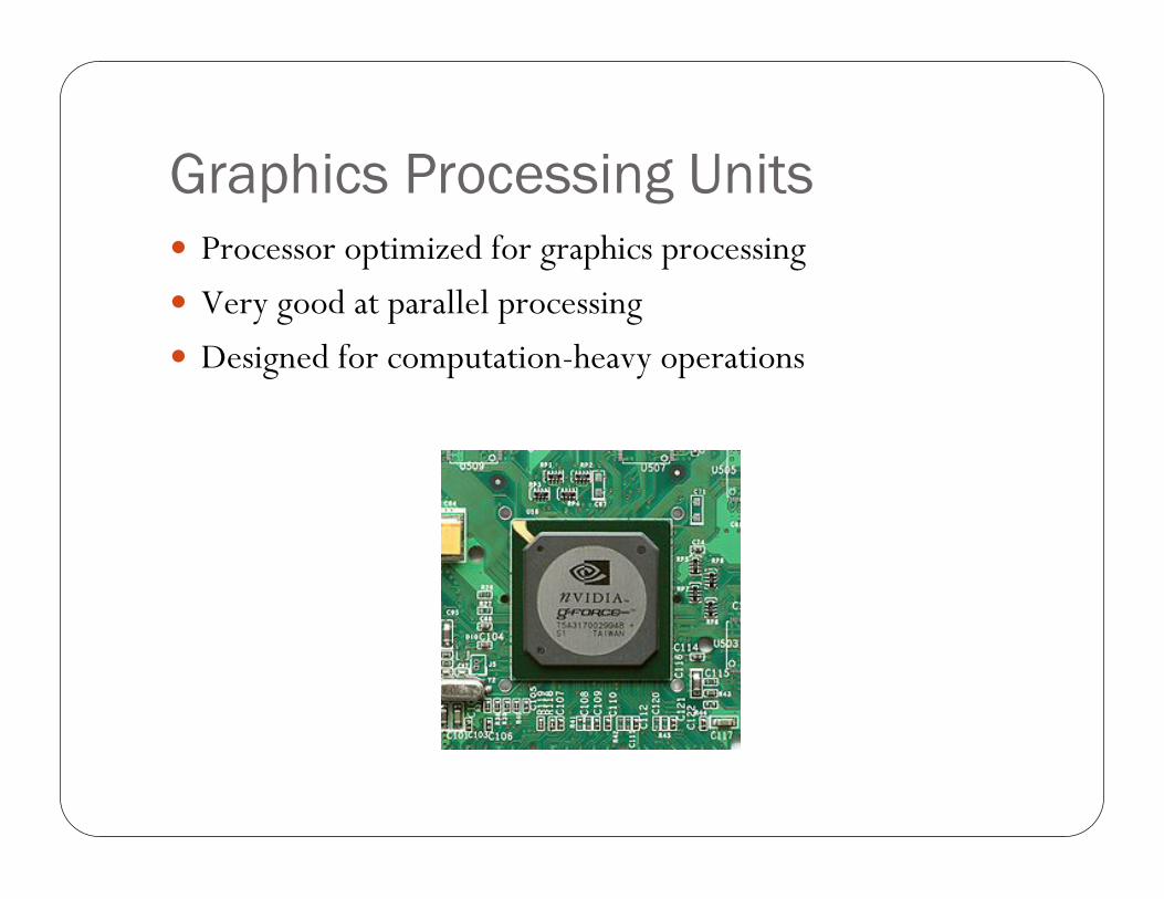
Graphics Processing UnitsProcessor optimized for graphics processing
Very good at parallel processing
Designed for computation-heavy operations
Graphics History1981: First PC video cards created by IBM
1984: First processor-based graphics card
1990’s: Advent of 3D graphics, advancements driven by gaming/CAD (Computer Aided Design)
1992: OpenGL application programming interface introduced
1999: Nvidia GeForce 256 marketed as “world’s first GPU”
2000’s – present: Increased programmability (DirectX), general purpose usage (GPGPU)
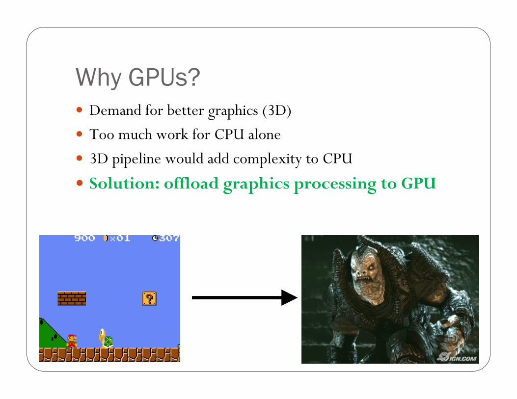
Why GPUs?Demand for better graphics (3D)
Too much work for CPU alone
3D pipeline would add complexity to CPU
Solution: offload graphics processing to GPU
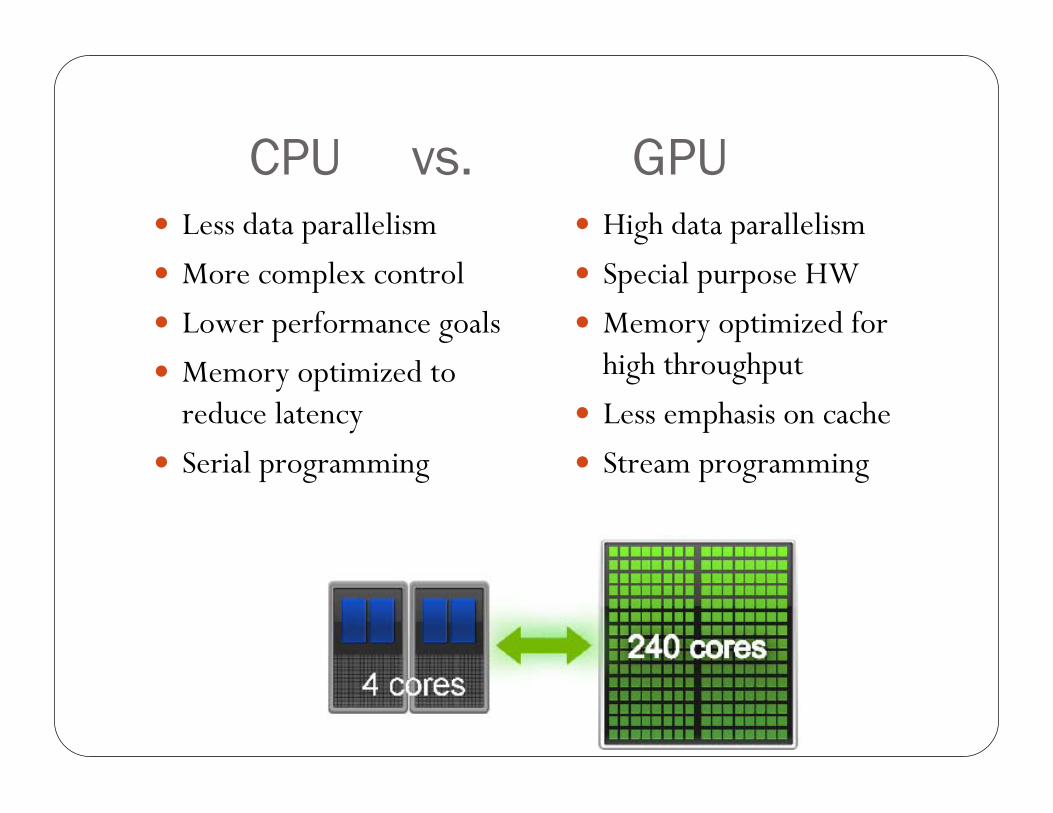
CPU vs. GPULess data parallelism
More complex control
Lower performance goals
Memory optimized to reduce latency
Serial programming
High data parallelism
Special purpose HW
Memory optimized for high throughput
Less emphasis on cache
Stream programming
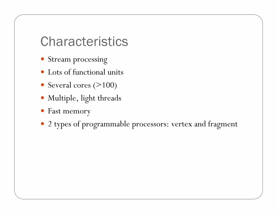
CharacteristicsStream processing
Lots of functional units
Several cores (>100)
Multiple, light threads
Fast memory
2 types of programmable processors: vertex and fragment
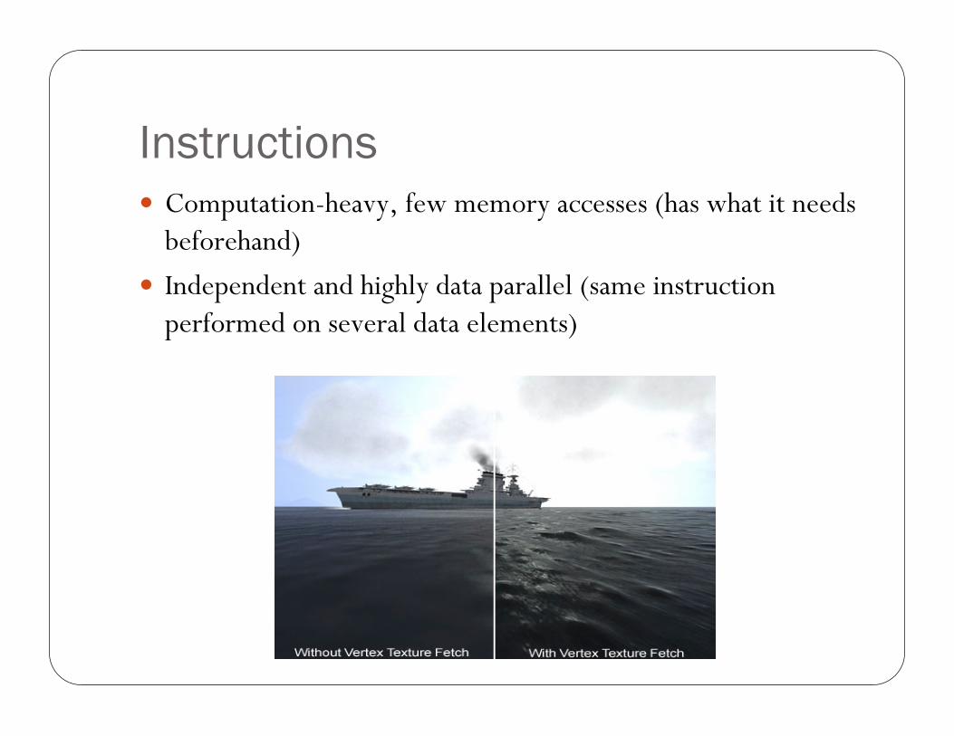
InstructionsComputation-heavy, few memory accesses (has what it needs beforehand)
Independent and highly data parallel (same instruction performed on several data elements)
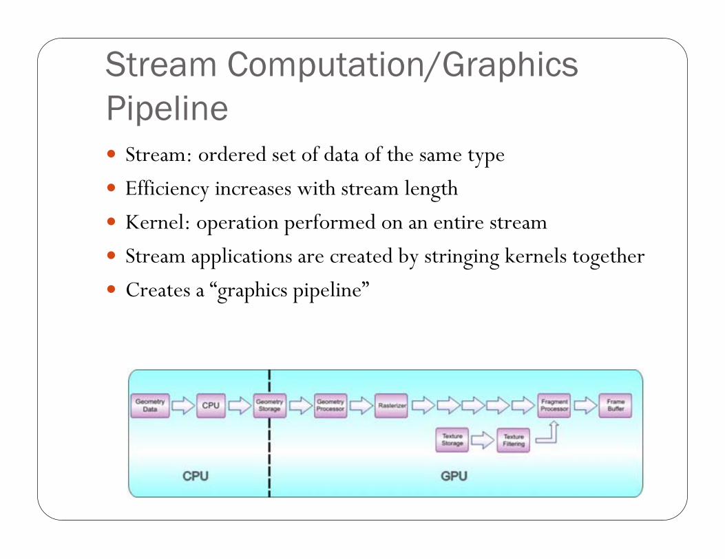
Stream Computation/Graphics Pipeline
Stream: ordered set of data of the same type
Efficiency increases with stream length
Kernel: operation performed on an entire stream
Stream applications are created by stringing kernels together
Creates a “graphics pipeline”
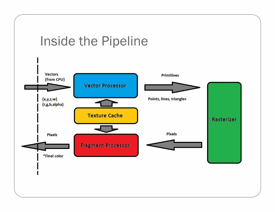
Inside the Pipeline
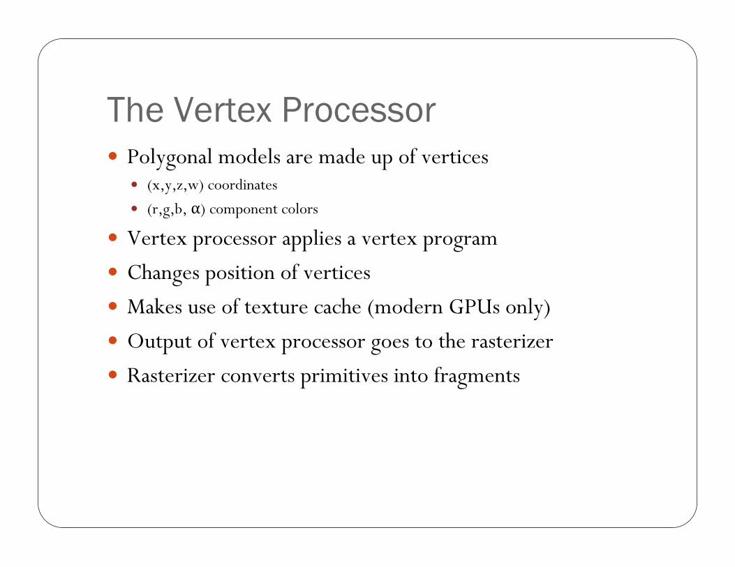
The Vertex ProcessorPolygonal models are made up of vertices
(x,y,z,w) coordinates
(r,g,b, α) component colors
Vertex processor applies a vertex program
Changes position of vertices
Makes use of texture cache (modern GPUs only)
Output of vertex processor goes to the rasterizer
Rasterizer converts primitives into fragments
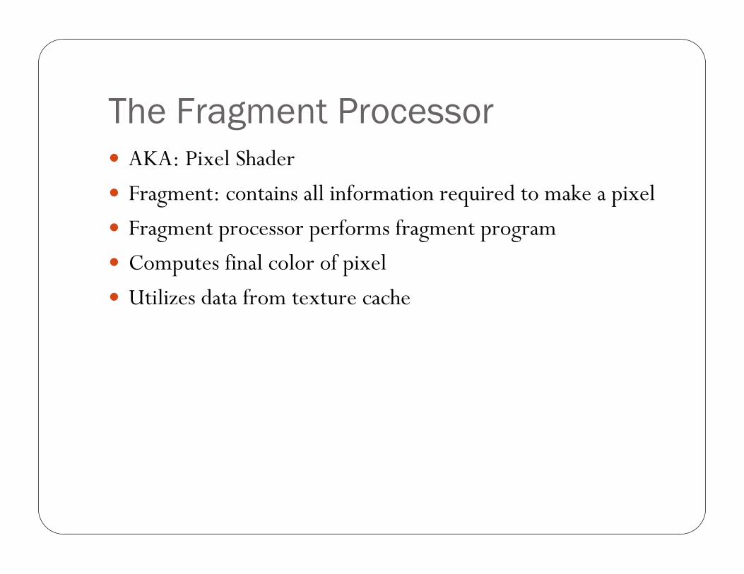
The Fragment ProcessorAKA: Pixel Shader
Fragment: contains all information required to make a pixel
Fragment processor performs fragment program
Computes final color of pixel
Utilizes data from texture cache
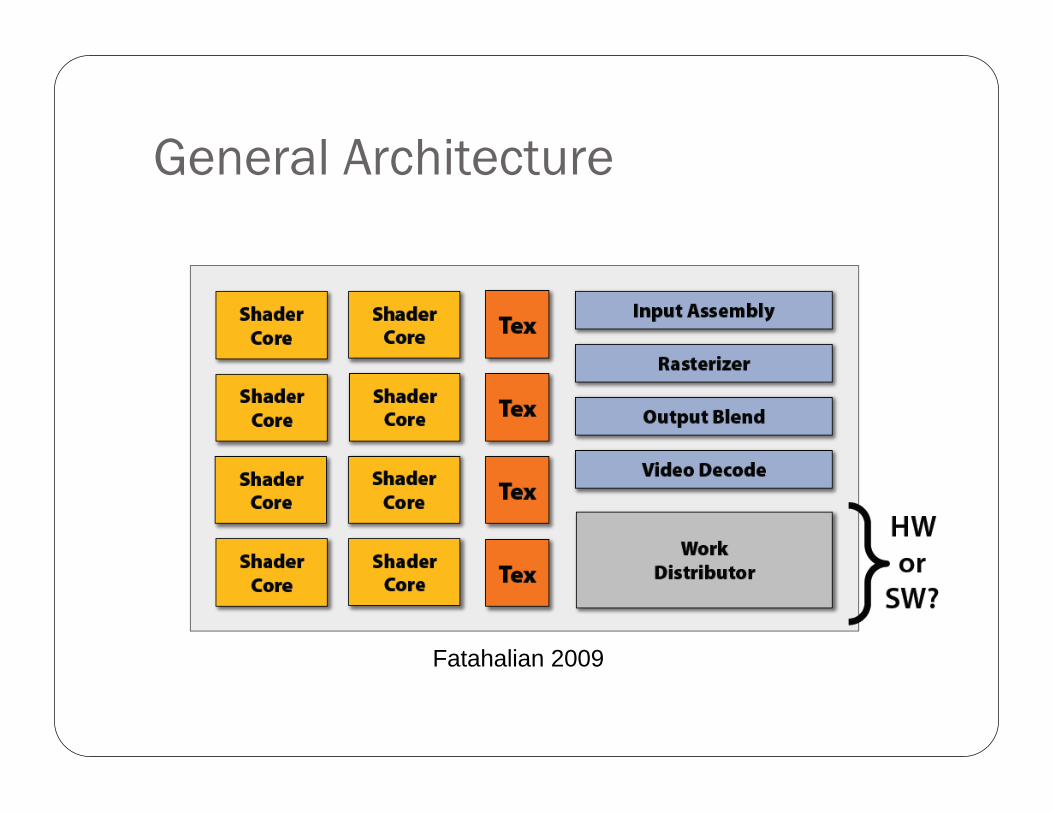
General Architecture
Fatahalian 2009
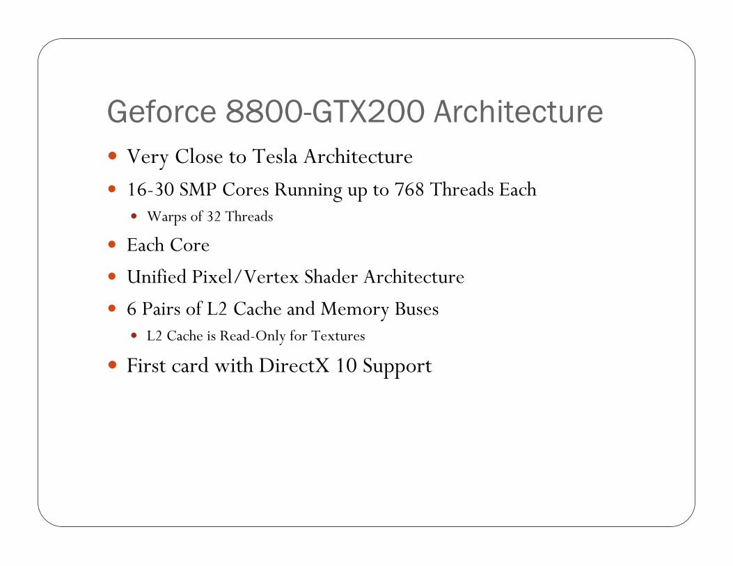
Geforce 8800-GTX200 ArchitectureVery Close to Tesla Architecture16-30 SMP Cores Running up to 768 Threads Each
Warps of 32 Threads
Each Core
Unified Pixel/Vertex Shader Architecture
6 Pairs of L2 Cache and Memory BusesL2 Cache is Read-Only for Textures
First card with DirectX 10 Support
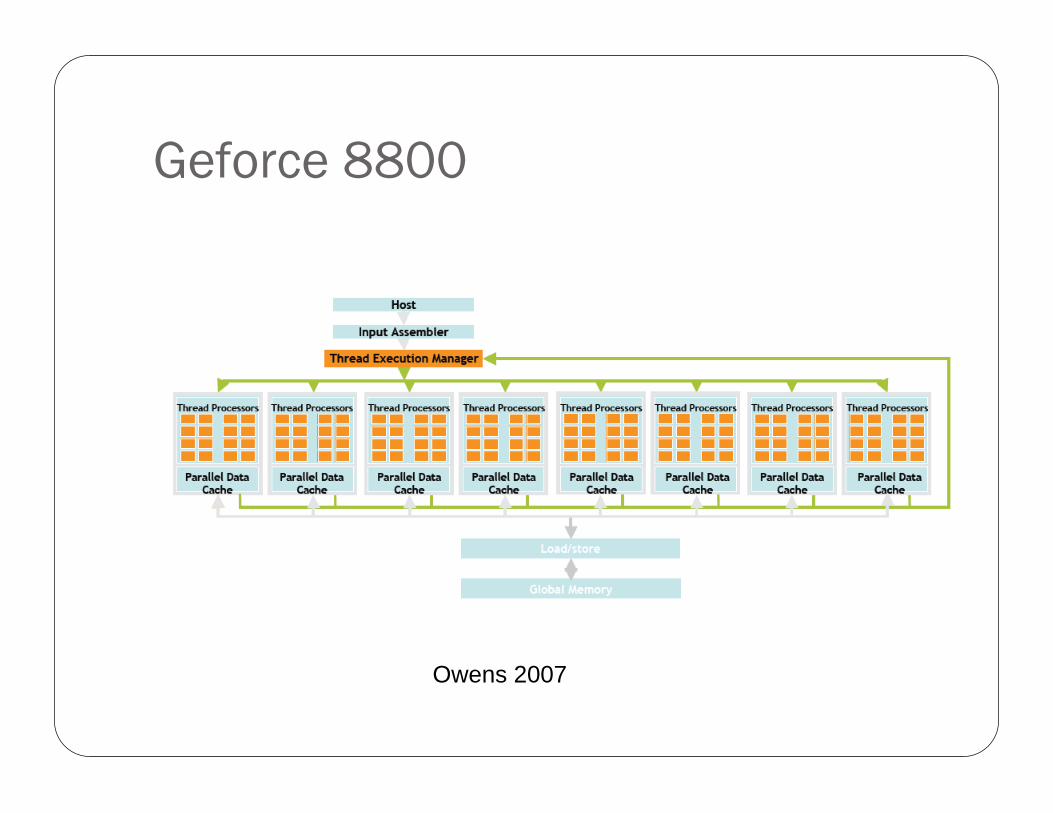
Geforce 8800
Owens 2007
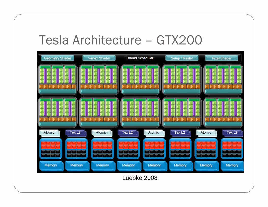
Tesla Architecture – GTX200
Luebke 2008
Fermi Architecture40nm Process, 3 Billion Transistors
512 CUDA cores organized into 16 SMPsEach supporting up to 1536 simultaneous threads
16 Load/Store, 16 ALU, 4 Special Purpose Units Each
6 GDDR5 DRAM Interfaces, 40 bit Addresses
Cores Clocked at 1.3Ghz+, while Cache is at 600Mhz
Fermi ArchitectureEmbedded Unified Shader Architecture
Incorporates Tessellation into Vertex, Geometry, and Pixel Shading
8x Double Precision FP Performance over Tesla
Distributed Rasterizer
L1 Cache - Register Spilling, Stack Operations, and Load/Store only
L2 Cache – For Textures, Read/Write
ECC Memory Protection
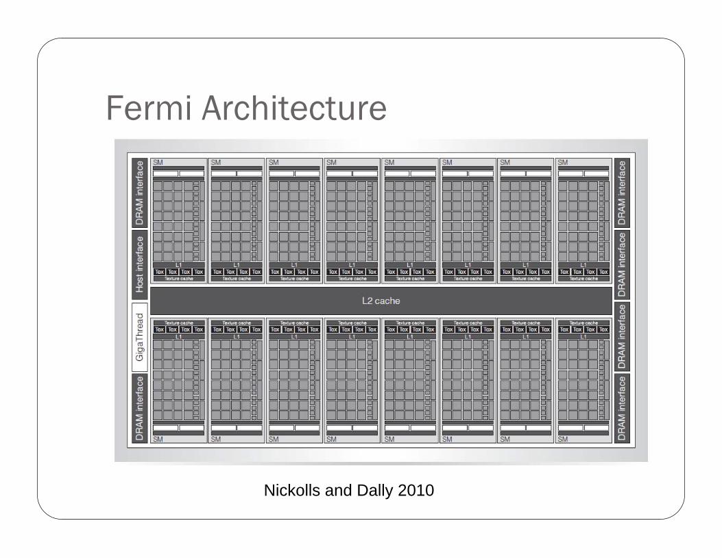
Fermi Architecture
Nickolls and Dally 2010
AMD’s Cayman Architecture40nm Technology, 2.64 Billion Transistors
24 880Mhz CoresEach Running 4-Wide VLIW Instructions
Static Scheduling8KB L1 Texture CacheShared L2 Cache4KB Write Cache
OpenCL and DirectCompute instead of CUDA
Interleaved ALU FunctionsAll ALU/Execution Units are same, no special units
7840KB of Registers
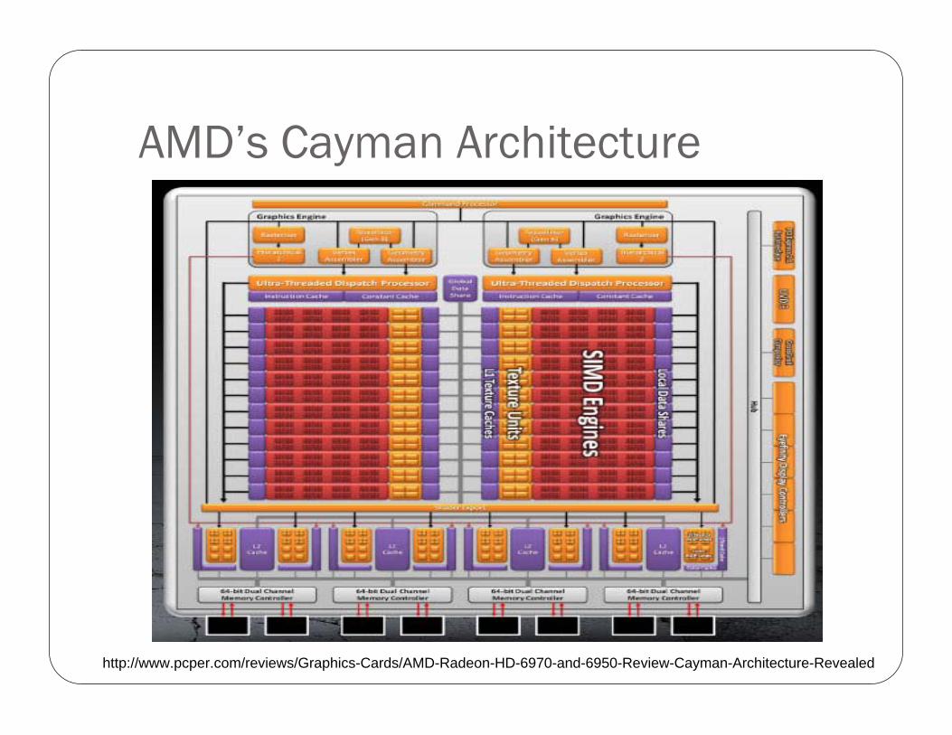
AMD’s Cayman Architecture
http://www.pcper.com/reviews/Graphics-Cards/AMD-Radeon-HD-6970-and-6950-Review-Cayman-Architecture-Revealed
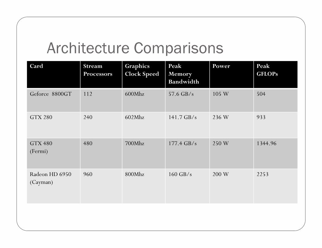
Architecture ComparisonsCard Stream
ProcessorsGraphicsClock Speed
Peak MemoryBandwidth
Power PeakGFLOPs
Geforce 8800GT 112 600Mhz 57.6 GB/s 105 W 504
GTX 280 240 602Mhz 141.7 GB/s 236 W 933
GTX 480(Fermi)
480 700Mhz 177.4 GB/s 250 W 1344.96
Radeon HD 6950(Cayman)
960 800Mhz 160 GB/s 200 W 2253
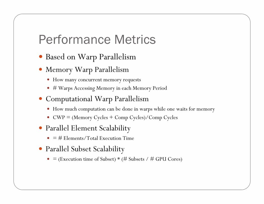
Performance MetricsBased on Warp ParallelismMemory Warp Parallelism
How many concurrent memory requests
# Warps Accessing Memory in each Memory Period
Computational Warp Parallelism How much computation can be done in warps while one waits for memory
CWP = (Memory Cycles + Comp Cycles)/Comp Cycles
Parallel Element Scalability= # Elements/Total Execution Time
Parallel Subset Scalability= (Execution time of Subset) * (# Subsets / # GPU Cores)
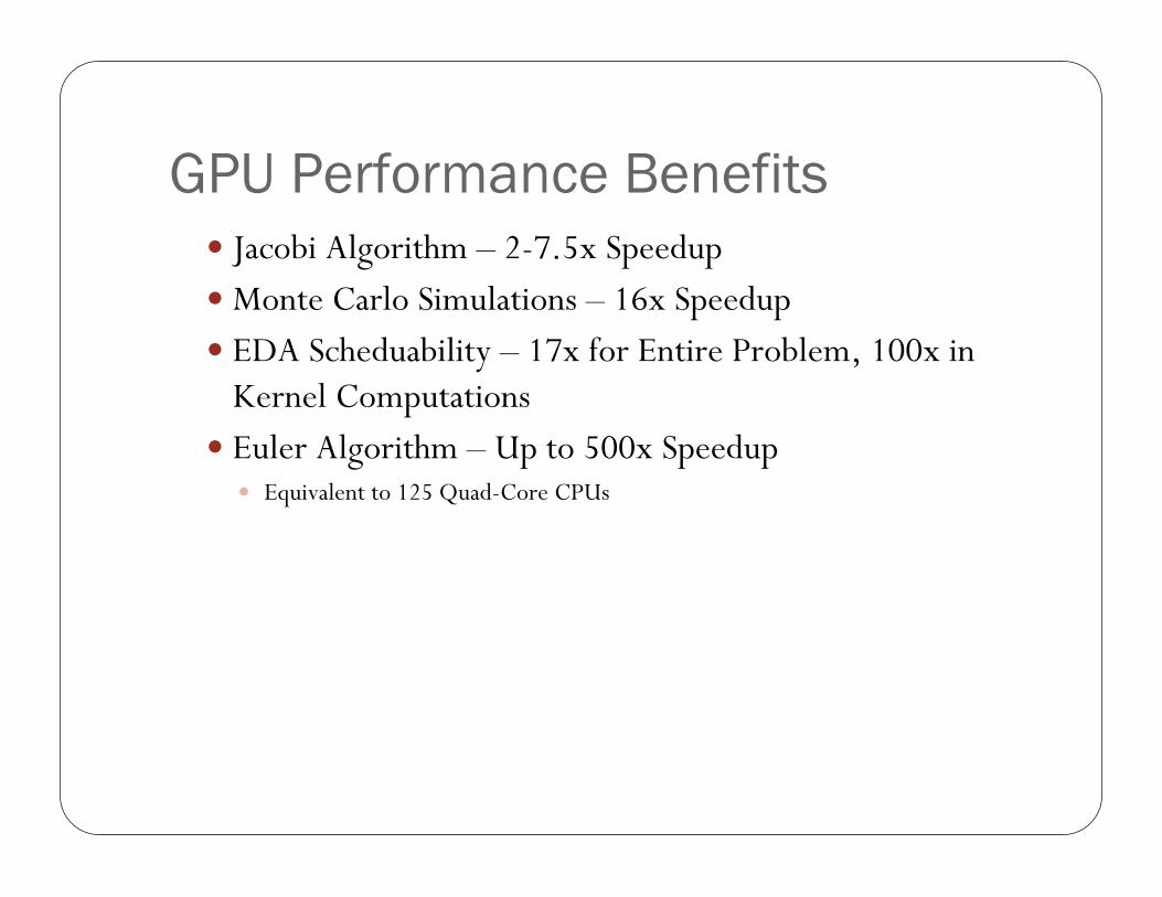
GPU Performance BenefitsJacobi Algorithm – 2-7.5x SpeedupMonte Carlo Simulations – 16x SpeedupEDA Scheduability – 17x for Entire Problem, 100x in Kernel ComputationsEuler Algorithm – Up to 500x Speedup
Equivalent to 125 Quad-Core CPUs
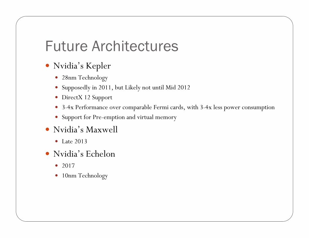
Future ArchitecturesNvidia’s Kepler
28nm Technology
Supposedly in 2011, but Likely not until Mid 2012
DirectX 12 Support
3-4x Performance over comparable Fermi cards, with 3-4x less power consumption
Support for Pre-emption and virtual memory
Nvidia’s MaxwellLate 2013
Nvidia’s Echelon2017
10nm Technology
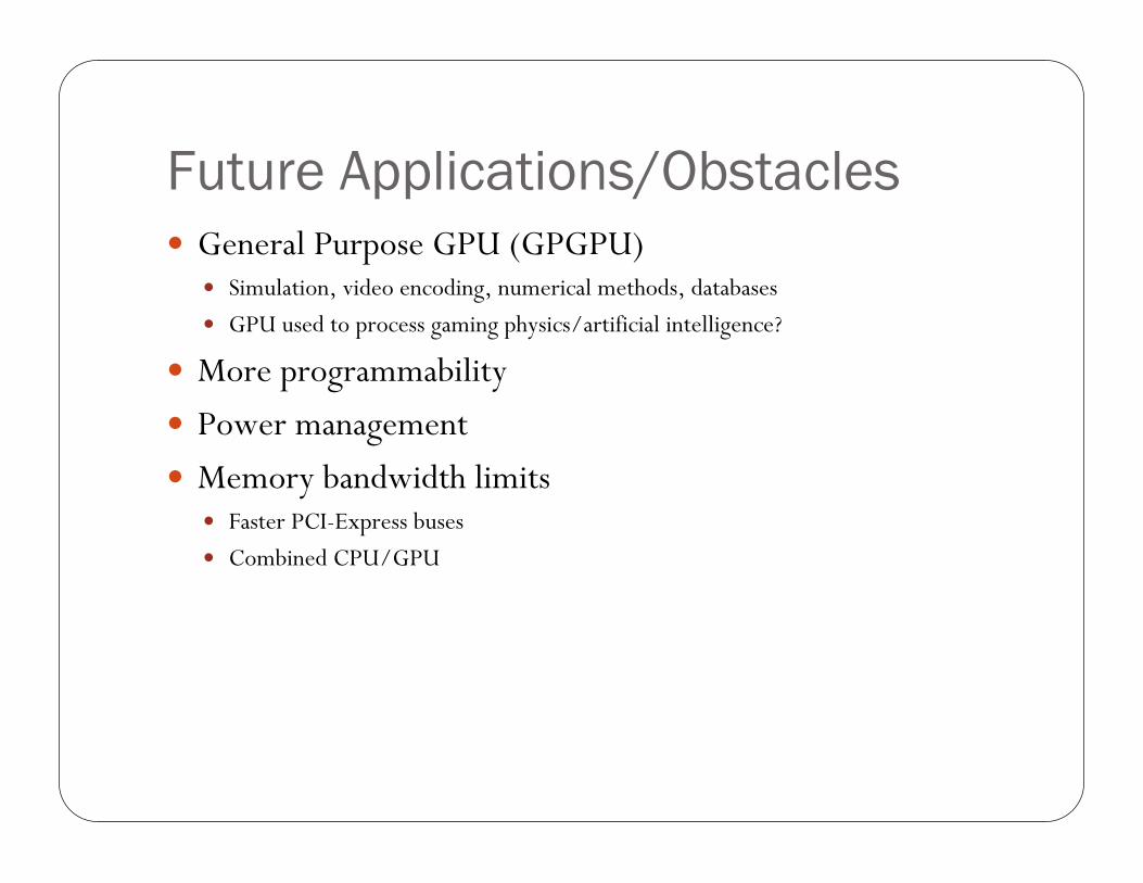
Future Applications/ObstaclesGeneral Purpose GPU (GPGPU)
Simulation, video encoding, numerical methods, databases
GPU used to process gaming physics/artificial intelligence?
More programmability
Power management
Memory bandwidth limitsFaster PCI-Express buses
Combined CPU/GPU
Questions?