graphics processing unit - study...
TRANSCRIPT

www.studymafia.org
A
Seminar report
On
Graphics Processing Unit Submitted in partial fulfillment of the requirement for the award of degree
of Bachelor of Technology in Computer Science
SUBMITTED TO: SUBMITTED BY: www.studymafia.org www.studymafia.org

www.studymafia.org
Acknowledgement
I would like to thank respected Mr…….. and Mr. ……..for giving me such a
wonderful opportunity to expand my knowledge for my own branch and giving me
guidelines to present a seminar report. It helped me a lot to realize of what we study for.
Secondly, I would like to thank my parents who patiently helped me as i went through
my work and helped to modify and eliminate some of the irrelevant or un-necessary
stuffs.
Thirdly, I would like to thank my friends who helped me to make my work more
organized and well-stacked till the end.
Next, I would thank Microsoft for developing such a wonderful tool like MS Word. It
helped my work a lot to remain error-free.
Last but clearly not the least, I would thank The Almighty for giving me strength to
complete my report on time.

www.studymafia.org
Preface
I have made this report file on the topic Graphics Processing Unit; I have tried my best
to elucidate all the relevant detail to the topic to be included in the report. While in the
beginning I have tried to give a general view about this topic.
My efforts and wholehearted co-corporation of each and everyone has ended on a
successful note. I express my sincere gratitude to …………..who assisting me
throughout the preparation of this topic. I thank him for providing me the
reinforcement, confidence and most importantly the track for the topic whenever I
needed it.

www.studymafia.org
CONTENTS
1. INTRODUCTION
2. WHAT’S A GPU ???
3. HISTORY AND STANDARDS
4. PERIPHERAL COMPONENT INTERCONNECT
5. ACCELLERATED GRAPHICS PORT
6. COMPONENTS OF GPU
7. HOW IS 3D ACCELLERATION DONE ?
8. PERFORMANCE FACTOR OF GPU
9. TYPES OF GPU
10. GEFORCE4
11. GEFORCE4 TI
12. GEFORCE4 MX
13. GEFORCE4 GO
14. CONCLUSION
15. 3D GLOSSARY
16. REFERENCES
www.studymafia.org
INTRODUCTION
There are various applications that require a 3D world to be simulated as realistically
as possible on a computer screen. These include 3D animations in games, movies and
other real world simulations. It takes a lot of computing power to represent a 3D
world due to the great amount of information that must be used to generate a realistic
3D world and the complex mathematical operations that must be used to project this
3D world onto a computer screen. In this situation, the processing time and
bandwidth are at a premium due to large amounts of both computation and data.
The functional purpose of a GPU then, is to provide a separate dedicated
graphics resources, including a graphics processor and memory, to relieve some of
the burden off of the main system resources, namely the Central Processing Unit,
Main Memory, and the System Bus, which would otherwise get saturated with
graphical operations and I/O requests. The abstract goal of a GPU, however, is to
enable a representation of a 3D world as realistically as possible. So these GPUs are
designed to provide additional computational power that is customized specifically to
perform these 3D tasks.

www.studymafia.org
WHAT’S A GPU????
A Graphics Processing Unit (GPU) is a microprocessor that has been
designed specifically for the processing of 3D graphics. The processor is built with
integrated transform, lighting, triangle setup/clipping, and rendering engines, capable
of handling millions of math-intensive processes per second. GPUs form the heart of
modern graphics cards, relieving the CPU (central processing units) of much of the
graphics processing load. GPUs allow products such as desktop PCs, portable
computers, and game consoles to process real-time 3D graphics that only a few years
ago were only available on high-end workstations.
Used primarily for 3-D applications, a graphics processing unit is a single-
chip processor that creates lighting effects and transforms objects every time a 3D
scene is redrawn. These are mathematically-intensive tasks, which otherwise, would
put quite a strain on the CPU. Lifting this burden from the CPU frees up cycles that
can be used for other jobs.
However, the GPU is not just for playing 3D-intense videogames or for those
who create graphics (sometimes referred to as graphics rendering or content-creation)
but is a crucial component that is critical to the PC's overall system speed. In order to
fully appreciate the graphics card's role it must first be understood.
Many synonyms exist for Graphics Processing Unit in which the popular
one being the graphics card .It’s also known as a video card, video accelerator, video
adapter, video board, graphics accelerator, or graphics adapter.

www.studymafia.org
HISTORY AND STANDARDS
The first graphics cards, introduced in August of 1981 by IBM, were
monochrome cards designated as Monochrome Display Adapters (MDAs). The
displays that used these cards were typically text-only, with green or white text on a
black background. Color for IBM-compatible computers appeared on the scene with
the 4-color Hercules Graphics Card (HGC), followed by the 8-color Color
Graphics Adapter (CGA) and 16-color Enhanced Graphics Adapter (EGA).
During the same time, other computer manufacturers, such as Commodore, were
introducing computers with built-in graphics adapters that could handle a varying
number of colors.
When IBM introduced the Video Graphics Array (VGA) in 1987, a new
graphics standard came into being. A VGA display could support up to 256 colors
(out of a possible 262,144-color palette) at resolutions up to 720x400. Perhaps the
most interesting difference between VGA and the preceding formats is that VGA was
analog, whereas displays had been digital up to that point. Going from digital to
analog may seem like a step backward, but it actually provided the ability to vary the
signal for more possible combinations than the strict on/off nature of digital.
Over the years, VGA gave way to Super Video Graphics Array (SVGA).
SVGA cards were based on VGA, but each card manufacturer added resolutions and
increased color depth in different ways. Eventually, the Video Electronics
Standards Association (VESA) agreed on a standard implementation of SVGA that
provided up to 16.8 million colors and 1280x1024 resolution. Most graphics cards
available today support Ultra Extended Graphics Array (UXGA). UXGA can
support a palette of up to 16.8 million colors and resolutions up to 1600x1200 pixels.
Even though any card you can buy today will offer higher colors and resolution
than the basic VGA specification, VGA mode is the de facto standard for graphics
and is the minimum on all cards. In addition to including VGA, a graphics card must
be able to connect to your computer. While there are still a number of graphics cards

www.studymafia.org
that plug into an Industry Standard Architecture (ISA) or Peripheral Component
Interconnect (PCI) slot, most current graphics cards use the Accelerated Graphics
Port (AGP).
PERIPHERAL COMPONENT INTERCONNECT(PCI)
There are a lot of incredibly complex components in a computer. And all of
these parts need to communicate with each other in a fast and efficient manner.
Essentially, a bus is the channel or path between the components in a computer.
During the early 1990s, Intel introduced a new bus standard for consideration, the
Peripheral Component Interconnect (PCI).It provides direct access to system memory
for connected devices, but uses a bridge to connect to the front side bus and therefore
to the CPU.
The illustration above shows how the various buses connect to the CPU.
PCI can connect up to five external components. Each of the five connectors
for an external component can be replaced with two fixed devices on the
motherboard. The PCI bridge chip regulates the speed of the PCI bus independently

www.studymafia.org
of the CPU's speed. This provides a higher degree of reliability and ensures that PCI-
hardware manufacturers know exactly what to design for.
PCI originally operated at 33 MHz using a 32-bit-wide path. Revisions to the
standard include increasing the speed from 33 MHz to 66 MHz and doubling the bit
count to 64. Currently, PCI-X provides for 64-bit transfers at a speed of 133 MHz for
an amazing 1-GBps (gigabyte per second) transfer rate!
PCI cards use 47 pins to connect (49 pins for a mastering card, which can
control the PCI bus without CPU intervention). The PCI bus is able to work with so
few pins because of hardware multiplexing, which means that the device sends more
than one signal over a single pin. Also, PCI supports devices that use either 5 volts or
3.3 volts. PCI slots are the best choice for network interface cards (NIC), 2-D video
cards, and other high-bandwidth devices. On some PCs, PCI has completely
superseded the old ISA expansion slots.
Although Intel proposed the PCI standard in 1991, it did not achieve popularity
until the arrival of Windows 95 (in 1995). This sudden interest in PCI was due to the
fact that Windows 95 supported a feature called Plug and Play (PnP). PnP means
that you can connect a device or insert a card into your computer and it is
automatically recognized and configured to work in your system. Intel created the
PnP standard and incorporated it into the design for PCI. But it wasn't until several
years later that a mainstream operating system, Windows 95, provided system-level
support for PnP. The introduction of PnP accelerated the demand for computers with
PCI.
ACCELERATED GRAPHICS PORT (AGP)
The need for streaming video and real-time-rendered 3-D games requires an
even faster throughput than that provided by PCI. In 1996, Intel debuted the
www.studymafia.org
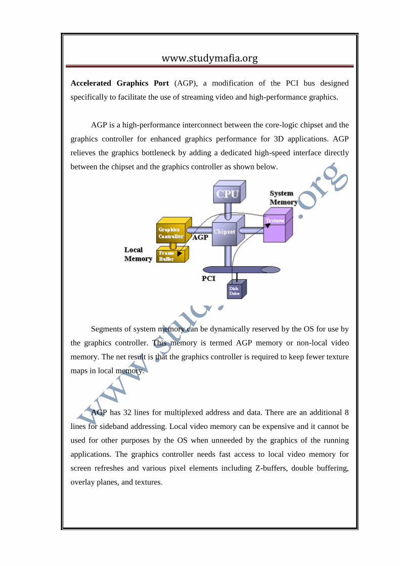
Accelerated Graphics Port (AGP), a modification of the PCI bus designed
specifically to facilitate the use of streaming video and high-performance graphics.
AGP is a high-performance interconnect between the core-logic chipset and the
graphics controller for enhanced graphics performance for 3D applications. AGP
relieves the graphics bottleneck by adding a dedicated high-speed interface directly
between the chipset and the graphics controller as shown below.
Segments of system memory can be dynamically reserved by the OS for use by
the graphics controller. This memory is termed AGP memory or non-local video
memory. The net result is that the graphics controller is required to keep fewer texture
maps in local memory.
AGP has 32 lines for multiplexed address and data. There are an additional 8
lines for sideband addressing. Local video memory can be expensive and it cannot be
used for other purposes by the OS when unneeded by the graphics of the running
applications. The graphics controller needs fast access to local video memory for
screen refreshes and various pixel elements including Z-buffers, double buffering,
overlay planes, and textures.

www.studymafia.org
For these reasons, programmers can always expect to have more texture
memory available via AGP system memory. Keeping textures out of the frame buffer
allows larger screen resolution, or permits Z-buffering for a given large screen size.
As the need for more graphics intensive applications continues to scale upward, the
amount of textures stored in system memory will increase. AGP delivers these
textures from system memory to the graphics controller at speeds sufficient to make
system memory usable as a secondary texture store.
AGP Memory Allocation
During AGP memory initialization, the OS allocates 4K byte pages of AGP
memory in main (physical) memory. These pages are usually discontiguous.
However, the graphics controller needs contiguous memory. A translation mechanism
called the GART (Graphics Address Remapping Table), makes discontiguous
memory appear as contiguous memory by translating virtual addresses into physical
addresses in main memory through a remapping table.
A block of contiguous memory space, called the Aperture is allocated above
the top of memory. The graphics card accesses the Aperture as if it were main
memory. The GART is then able to remap these virtual addresses to physical
addresses in main memory. These virtual addresses are used to access main memory,
the local frame buffer, and AGP memory.

www.studymafia.org
AGP Transfers
AGP provides two modes for the graphics controller to directly access texture
maps in system memory: pipelining and sideband addressing. Using Pipe mode,
AGP overlaps the memory or bus access times for a request ("n") with the issuing of
following requests ("n+1"..."n+2"... etc.). In the PCI bus, request "n+1" does not
begin until the data transfer of request "n" finishes.
With sideband addressing (SBA), AGP uses 8 extra "sideband" address lines which
allow the graphics controller to issue new addresses and requests simultaneously
while data continues to move from previous requests on the main 32 data/address
lines. Using SBA mode improves efficiency and reduces latencies.
AGP Specifications
The current PCI bus supports a data transfer rate up to 132 MB/s, while AGP
(at 66MHz) supports up to 533 MB/s! AGP attains this high transfer rate due to it's
ability to transfer data on both the rising and falling edges of the 66MHz clock
Mode Approximate Transfer rate

www.studymafia.org
clock rate (MBps)
1x 66 MHz 266
2x 133 MHz 533
4x 266 MHZ 1066
8x 533 MHZ 2133
The AGP slot typically provides performance which is 4 to 8 times faster than
the PCI slots inside your computer.
COMPONENTS OF GPU
There are several components on a typical graphics card:
Graphics Processor
The graphics processor is the brains of the card, and is typically one of three
configurations:
Graphics co-processor: A card with this type of processor can handle all of the
graphics chores without any assistance from the computer's CPU. Graphics co-
processors are typically found on high-end video cards.
Graphics accelerator: In this configuration, the chip on the graphics card renders
graphics based on commands from the computer's CPU. This is the most common
configuration used today.
Frame buffer: This chip simply controls the memory on the card and sends
information to the digital-to-analog converter (DAC) . It does no processing of the
image data and is rarely used anymore.

www.studymafia.org
Memory – The type of RAM used on graphics cards varies widely, but the most
popular types use a dual-ported configuration. Dual-ported cards can write to one
section of memory while it is reading from another section, decreasing the time it
takes to refresh an image.
Graphics BIOS – Graphics cards have a small ROM chip containing basic
information that tells the other components of the card how to function in relation to
each other. The BIOS also performs diagnostic tests on the card's memory and input/
output (I/O) to ensure that everything is functioning correctly.
Digital-to-Analog Converter (DAC) – The DAC on a graphics card is commonly
known as a RAMDAC because it takes the data it converts directly from the card's
memory. RAMDAC speed greatly affects the image you see on the monitor. This is
because the refresh rate of the image depends on how quickly the analog information
gets to the monitor.
Display Connector – Graphics cards use standard connectors. Most cards use the 15-
pin connector that was introduced with Video Graphics Array (VGA).
Computer (Bus) Connector – This is usually Accelerated Graphics Port (AGP).
This port enables the video card to directly access system memory. Direct memory
access helps to make the peak bandwidth four times higher than the Peripheral
Component Interconnect (PCI) bus adapter card slots. This allows the central
processor to do other tasks while the graphics chip on the video card accesses system
memory.
Internal Organization of GPU
Clock
Generator
Local Memory
Video IN/OUT
Local Bus
Graphics Processor
RAM
DAC
Graphics
Controller
VGA
BIOS
www.studymafia.org
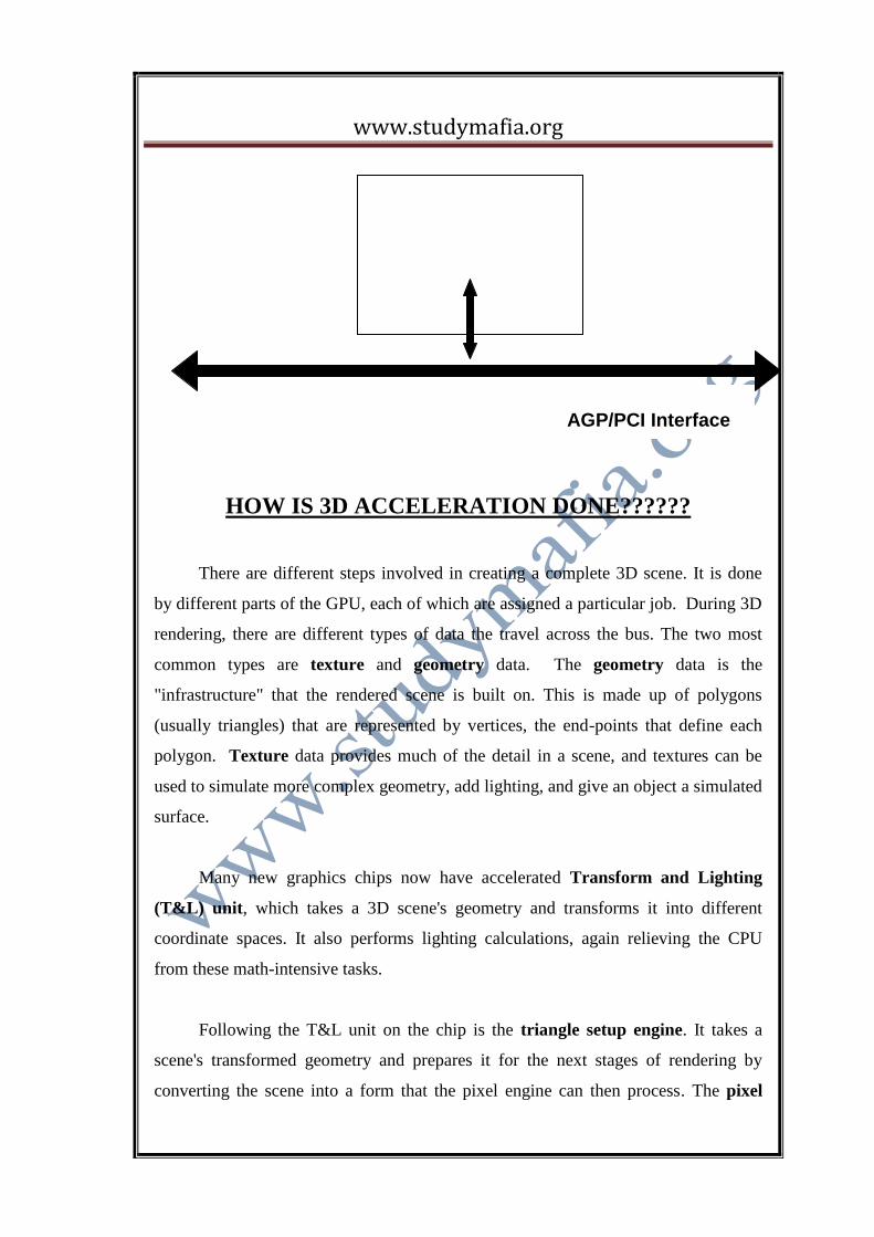
HOW IS 3D ACCELERATION DONE??????
There are different steps involved in creating a complete 3D scene. It is done
by different parts of the GPU, each of which are assigned a particular job. During 3D
rendering, there are different types of data the travel across the bus. The two most
common types are texture and geometry data. The geometry data is the
"infrastructure" that the rendered scene is built on. This is made up of polygons
(usually triangles) that are represented by vertices, the end-points that define each
polygon. Texture data provides much of the detail in a scene, and textures can be
used to simulate more complex geometry, add lighting, and give an object a simulated
surface.
Many new graphics chips now have accelerated Transform and Lighting
(T&L) unit, which takes a 3D scene's geometry and transforms it into different
coordinate spaces. It also performs lighting calculations, again relieving the CPU
from these math-intensive tasks.
Following the T&L unit on the chip is the triangle setup engine. It takes a
scene's transformed geometry and prepares it for the next stages of rendering by
converting the scene into a form that the pixel engine can then process. The pixel
AGP/PCI Interface
www.studymafia.org
engine applies assigned texture values to each pixel. This gives each pixel the correct
color value so that it appears to have surface texture and does not look like a flat,
smooth object. After a pixel has been rendered it must be checked to see whether it is
visible by checking the depth value, or Z value.
A Z check unit performs this process by reading from the Z-buffer to see
if there are any other pixels rendered to the same location where the new pixel
will be rendered. If another pixel is at that location, it compares the Z value of
the existing pixel to that of the new pixel. If the new pixel is closer to the view
camera, it gets written to the frame buffer. If it's not, it gets discarded. After the
complete scene is drawn into the frame buffer the RAMDAC converts this
digital data into analog that can be given to the monitor for display.
PERFORMANCE FACTORS OF GPU
There are many factors that affect the performance of a GPU. Some of the
factors that are directly visible to a user are given below.
Fill Rate:
It is defined as the number of pixels or texels (textured pixels) rendered per
second by the GPU on to the memory . It shows the true power of the GPU.
Modern GPUs have fill rates as high as 3.2 billion pixels. The fill rate of a GPU
can be increased by increasing the clock given to it.
Memory Bandwidth:
It is the data transfer speed between the graphics chip and its local frame
buffer. More bandwidth usually gives better performance with the image to be
rendered is of high quality and at very high resolution.
Memory Management:

www.studymafia.org
The performance of the GPU also depends on how efficiently the memory is
managed, because memory bandwidth may become the only bottle neck if not
managed properly.
Hidden Surface removal:
A term to describe the reducing of overdraws when rendering a scene by not
rendering surfaces that are not visible. This helps a lot in increasing the
performance of GPU, by preventing overdraw so that the fill rate of the GPU
can be utilized to the maximum.
Now lets see how far GPUs have come as far as performance is concerned.
0
100
200
300
400
500
600
700
800
900
1996 1997 1998 1999 2000 2001
Operations(Millions)/sec

www.studymafia.org
TYPES OF GPUS…
There are mainly two types of GPUs, they are
1. Those that can handle all of the graphics processes without any assistance
from the computer's CPU. They are typically found on high-end workstations.
These are mainly used for Digital Content Creation like 3D animation as it
supports a lot of 3D functions.
Some of them are……
Quadro series from NVIDIA.
Wildcat series from 3D Labs.
FireGL series from ATI.
2. The chip on the graphics card renders graphics based on commands
from the computer's CPU. This is the most common configuration used
today. These are used for 3D gaming and such smaller tasks. They are
found on normal desktop PCs and are better known as 3D accelerators. These
support less functions and hence are cheaper.
0
10
20
30
40
50
60
1996 1997 1998 1999 2000 2001
No of Transistors in Millions

www.studymafia.org
Some of them are…….
Geforce series from NVIDIA.
Radeon series from ATI Technology ltd.
Kyro series from STM Microelectronics
Today’s GPU can do what was hoped for and beyond. In the last year a giant
leap have been made in the GPU technology. The maximum amount of RAM that can
be found on a graphics card has jumped from 16MB to a whopping 128MB. The
premier company in GPU manufacturing ATI,who has held the position past couple
of years has given way to nVidia , whose new ground breaking technology is leaving
ATI to follow.
GEFORCE4
NVIDIA introduced the groundbreaking, top-to-bottom GeForce4 family of
GPUs—delivering new levels of graphics performance and display flexibility to
desktop and mobile PCs. nVidia’s latest creation, the GeForce4 GPU is the fourth
edition in the famed GeForce lineup. It has wowed gamers and artists alike by having
the capability to make graphics “better than life” with 128MB of DDR memory and a
super fast processor. What this means is that the GeForce4 is capable of rendering
graphics better than the eye can see. Although this is extraordinary, there are no
available monitors that can handle displaying such graphics. Even so, the nVIDIA
GeForce4 is truly an extraordinary and groundbreaking graphics processing unit.
GeForce4 is the most complete family of graphics solutions—from the
ferocious graphics power of the GeForce4 Ti, the world’s fastest GPU; to the multi-
display flexibility of the mainstream GeForce4 MX; to the most advanced mobile
graphics available, GeForce4 Go.
Three of its kind has been released…….
GeForce4 Ti series (NV25)
www.studymafia.org
GeForce4 MX series (NV17)
GeForce4 Go series
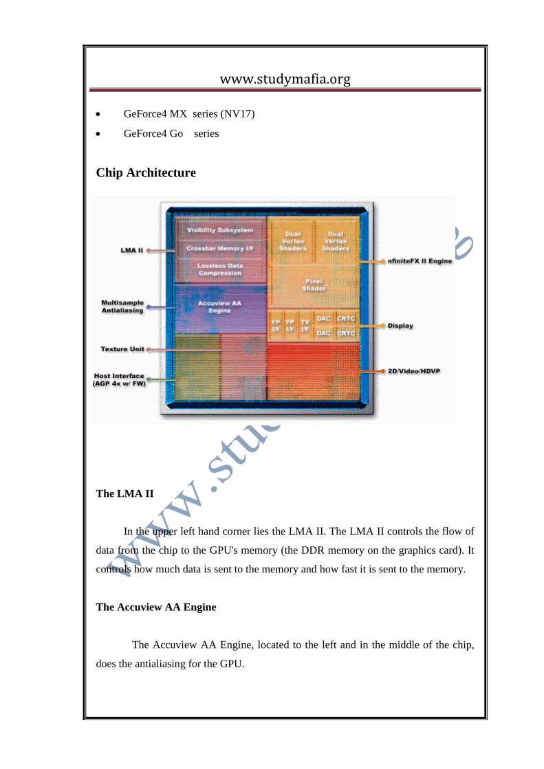
Chip Architecture
The LMA II
In the upper left hand corner lies the LMA II. The LMA II controls the flow of
data from the chip to the GPU's memory (the DDR memory on the graphics card). It
controls how much data is sent to the memory and how fast it is sent to the memory.
The Accuview AA Engine
The Accuview AA Engine, located to the left and in the middle of the chip,
does the antialiasing for the GPU.

www.studymafia.org
The Interface Unit
At the bottom of the GeForce4 chip and to the very left is the interface unit.
This simply determines what interface (2X or 4X AGP) the computer has, and adjusts
to comply with it.
The Texture Unit
At the bottom of the chip and to the left-center is the texture unit. This unit is
dedicated to processing textures that must be rendered.
The nfiniteFX II Engine
This is the striking feature of GeForce4 series.
One among the classic computer graphics problem have been regarding the
rendering the realistic hair and fur. Animals with skin texture were easy to render
than those with fur.
For the first time ever, and only through the power of nfiniteFX II engine, which
includes support for dual vertex shaders,advanced pixel shader pipelines , 3D
textures, shadow buffers and z-correct bump mapping ,is it now possible to
render those.
It also improves rendering of shading.

www.studymafia.org
A demo shot of a wolf man which has been rendered by GeForce4
The Display Unit
In the center to the right of the chip is the display unit. This unit is simple
and its only job is to determine the optimal display resolution for the display being
used. It also determines what type of display it is and optimizes its performance.
The 2D/Video/HDVP Unit
In the bottom right corner of the chip is the 2D/Video/HDVP unit. This part
of the chip is dedicated to all those tasks that don't require 3D rendering. These tasks
include movies, 2D pictures, 2D games and almost any other program that doesn't
have 3D graphics
nView Technology:
Simply put, NVIDIAs Multi-Monitor and Dual Independent Display
technology, now called "nView", has been polished up nicely. nView is available on
both the GF4 Ti and MX and enables the following:
Multi-desktop tools
Multi-desktop integration
Full featured interface including explorer browser with birds-eye views of
desktops
Toolbar control available as well for those needing a streamlined, low real-
estate interface
Window management
Individual application control
Window & dialog repositioning

www.studymafia.org
Application management
Transparency & colored transparency window options
Extends functionality of all applications
Pop- up menu control
GEFORCE4 TI
nVIDIA's crown graphics card is the GeForce4 Ti, a creation of admirable
brilliance. Its basic specifications include
63 million transistors (only 3 million more than GeForce3)
Manufactured in TSMC's .15 µ process
Chip clock 225 - 300 MHz
Memory clock 500 - 650 MHz
Memory bandwidth 8,000 - 10,400 MB/s
TnL Performance of 75 - 100 million vertices/s
128 MB frame buffer by default
nfiniteFX II engine
Accuview Anti Aliasing
Light Speed Memory Architecture II
nView
It has a 128 bit bus , double the size of previous busses and the only
graphics card to have one. This extra bus size improves performance dramatically. Its
considered as the world’s fastest GPU available today.
NV25 series include four- GeForce4 Ti 4600 ,GeForce4 Ti 4400 , GeForce4 Ti 4200
& GeForce4 Ti 4200 w/AGP 8x

www.studymafia.org
This chart shows comparison of performances of GeForce4 Ti 4600 and its predecessor in FPS.
GEFORCE4 MX
With the GeForce4 MX graphics processing units (GPUs), NVIDIA provides
a new level of cost-effective, high-performance graphics to the mainstream PC user.
The GeForce4 MX is the cheapest and worst performing of the three lines. The
standard graphics card comes with 64MB of RAM, a hefty amount that can handle
almost any task. The GeForce4 MX has a 64bit bus, which is also pretty standard for
today's graphics cards. For the most part the only real improvement from the
GeForce3 MX to the GeForce4MX is the graphics processing unit, which beats its
predecessors, the GeForce2 and GeForce3, hands down.
Performance comparisons

www.studymafia.org
GEFORCE4 GO
NVIDIA introduces the fastest, most comprehensive and feature-rich
computing experience ever realized on a mobile platform— the GeForce4 Go. With a
revolutionary core of integrated technologies, the GeForce4 Go ensures unparalleled
performance, battery life, and DVD and video playback. From notebooks powerful
enough to replace your desktop PC, to those that are both thin and light, NVIDIA's
GeForce4 Go mobile GPUs provide unprecedented mobile computing experiences.
CONCLUSION
From the introduction of the first 3D accelerator from 3dfx in 1996 these
units have come a long way to be truly called a “Graphics Processing Unit”. So it is
not a wonder that this piece of hardware is often referred to as an exotic product as far
as computer peripherals are concerned. By observing the current pace at which work
is going on in developing GPUs we can surely come to a conclusion that we will be
able to see better and faster GPUs in the near future.

www.studymafia.org
REFERENCES
1. www.howstuffworks.com
2. www.tomshardware.com
3. www.intel.com
4. www.nvidia.com
5. www.extremetech.com
6. www.pcworld.com