greetings from georgia institute of technology 3d...
TRANSCRIPT

IEEE Santa Clara Valley Chapter, Components, Packaging & Manufacturing Technology Society
10/12/2010
www.cpmt.org/scv 1
Greetings from Greetings from Georgia Institute of TechnologyGeorgia Institute of Technology
3D Systems Packaging Research Center3D Systems Packaging Research Centery g gy g g
IEEE CPMT, San Jose, CAIEEE CPMT, San Jose, CAOct12, 2010Oct12, 2010
Moore’s Law for SystemMoore’s Law for System IntegrationIntegrationFocusFocus of Last 50 Years; Moore’s Law for ICsof Last 50 Years; Moore’s Law for ICs
FocusFocus of Next 50 Years; Moore’s Law for Systemsof Next 50 Years; Moore’s Law for Systems
CoCo--Contributors:Contributors:TapobrataTapobrata BandyopadhyayBandyopadhyay, , NiteshNitesh KumbhatKumbhat, , RaghuRaghu PuchaPucha,,
Raj Raj PulugurthaPulugurtha, , HimaniHimani Sharma, Sharma, VenkyVenky Sundaram, Dean SutterSundaram, Dean Sutter
Prof. Prof. RaoRao R. TummalaR. TummalaDirector, 3D Systems Packaging Research CenterDirector, 3D Systems Packaging Research Center
Joseph M. Pettit Endowed Chair Joseph M. Pettit Endowed Chair Professor in ECE & MSEProfessor in ECE & MSE
GT PRCGT PRC
Began as an NSF ERCBegan as an NSF ERC Home for SOP ConceptHome for SOP Concept Home for SOP ConceptHome for SOP Concept Integrated Approach to Research Education & Industry Integrated Approach to Research Education & Industry
CollaborationCollaboration
1. Leading Edge 1. Leading Edge 3D Systems 3D Systems
R&DR&D
2.2. Educate Educate Future Future
LeadersLeaders
3.3. Collaborate Collaborate with Global with Global Industry & Industry & AcademicsAcademics
4.4. Enabled by Enabled by $40M 300mm $40M 300mm SOP FacilitySOP Facility
3D Systems Center3D Systems Center
Digital, RF & Bio ConvergenceDigital, RF & Bio Convergence
20 Academic & Research Faculty 20 Academic & Research Faculty
70 Global Companies70 Global Companies
1 | IEEE CPMT

IEEE Santa Clara Valley Chapter, Components, Packaging & Manufacturing Technology Society
10/12/2010
www.cpmt.org/scv 2
GT PRC as An Academic Leader GT PRC as An Academic Leader Economics Economics
•• Generated $247M research and infrastructure dollarsGenerated $247M research and infrastructure dollars•• Collaborated with 198 companies,15 government agenciesCollaborated with 198 companies,15 government agencies•• Created 4 spinCreated 4 spin--out and 4 spinout and 4 spin--in companiesin companies•• Contributed $351M to State of Georgia economyContributed $351M to State of Georgia economy
LeadingLeading--Edge Research:Edge Research:•• 1,200 refereed journal papers1,200 refereed journal papers•• > 249 invention disclosures> 249 invention disclosures•• 36 patents awarded; 6 patents pending36 patents awarded; 6 patents pending•• 166 royalty/royalty166 royalty/royalty--free licensesfree licenses•• 97 documented tech transfers97 documented tech transfers97 documented tech transfers97 documented tech transfers•• $40M state$40M state--ofof--thethe--art laboratoriesart laboratories•• Received 50 Best Paper awardsReceived 50 Best Paper awards
EducationEducation•• Granted 181 B.S, 283 M.S and 198 Ph.D. degreesGranted 181 B.S, 283 M.S and 198 Ph.D. degrees•• Designed 10 undergrad and 19 graduate crossDesigned 10 undergrad and 19 graduate cross--discipline coursesdiscipline courses•• Published 4 text/reference booksPublished 4 text/reference books
2 | IEEE CPMT
Presentation SummaryPresentation Summary
Si CMOS expected to reach limits due to:Si CMOS expected to reach limits due to:•• Leakage and Performance Leakage and Performance
•• Potential Solutions: FD SOI, Fin FET, 3D ICsPotential Solutions: FD SOI, Fin FET, 3D ICs
3D ICs coupled with 2D ICs poised to be strategic 3D ICs coupled with 2D ICs poised to be strategic Systems need more than 2D & 3D ICs for highestSystems need more than 2D & 3D ICs for highest--functionality at functionality at
lowest cost and in smallest sizelowest cost and in smallest size Moore’s Law for System Integration (MLSI) addresses this Moore’s Law for System Integration (MLSI) addresses this
bottleneckbottleneck Quantum jump in systems requires more than runQuantum jump in systems requires more than run--ofof--thethe--mill mill
f t if t imanufacturingmanufacturing MLSI requires new and fundamental concepts in Electrical, MLSI requires new and fundamental concepts in Electrical,
Mechanical, Chemical, Thermal, Bio, Material Sciences, Mechanical, Chemical, Thermal, Bio, Material Sciences, Engineering and ManufacturingEngineering and Manufacturing
MLSI provides unique and challenging opportunities in MLSI provides unique and challenging opportunities in interdisciplinary research, education, and industry collaborationinterdisciplinary research, education, and industry collaboration
3 | IEEE CPMT

IEEE Santa Clara Valley Chapter, Components, Packaging & Manufacturing Technology Society
10/12/2010
www.cpmt.org/scv 3
W/S
PC - Digital / cm
3 )
Georgia Tech PRC VisionGeorgia Tech PRC Vision
1000
10000
100000
olu
me(
cm3 )
SINGLE FUNCTIONDigital
Laptop
g
Notebook
Smart Phone
y o
r C
om
po
nen
t D
ensi
ty
MULTI FUNCTIONSMART
1970 1980 1990 2000
100
Vo
Fu
nct
ion
al D
ensi
tyMULTI -FUNCTION Digital, RF, MEMS, analog, video
“Watch” & Bio-sensor
MEGA-FUNCTION-Vision of GT PRC all the above and thousands of sensors
4 | IEEE CPMT
MultiMulti--Functional Consumer ElectronicsFunctional Consumer Electronics
LG Video Phone WatchLG Video Phone Watch
Featuring:Featuring:
Apple’s Apple’s iPhoneiPhone 44
Featuring:Featuring:•• Full touch screenFull touch screen
•• CameraCamera
•• SpeakerSpeaker
•• BluetoothBluetooth
Bionic gadget can:Bionic gadget can:•• Play music Play music
•• Take photosTake photos
•• Schedule apptsSchedule appts
•• MultiMulti--touch displaytouch display
•• Dual camerasDual cameras
•• ThreeThree--axis gyroscopeaxis gyroscope
•• Camera and LEDCamera and LED
BBionic gadget can:ionic gadget can:•• Play music, moviesPlay music, movies
•• Take photosTake photos
•• Record videosRecord videosSchedule apptsSchedule appts
•• Read text messagesRead text messages
•• Make video callsMake video calls
Record videosRecord videos
•• StreamStream TV showsTV shows
•• LocateLocate nearest Metro nearest Metro station in Parisstation in Paris
•• OverOver 200,000 200,000 applicationsapplications
5 | IEEE CPMT

IEEE Santa Clara Valley Chapter, Components, Packaging & Manufacturing Technology Society
10/12/2010
www.cpmt.org/scv 4
Georgia TechGeorgia Tech--PRC Vision of 3D PRC Vision of 3D SystemsSystems
Traditional Si CMOS New Devices
130nm 90nm 45nm 32nm 22nm 16nm 10nm
Moore’s Law in 2DMoore’s Law in 2D Packaging of 2D DevicesPackaging of 2D Devices
6 | IEEE CPMT
Georgia TechGeorgia Tech--PRC Vision of 3D PRC Vision of 3D SystemsSystems
Memory Logic Memory
Power Sensors Logic Memory
130nm 90nm 45nm 32nm 22nm 16nm 10nm
Moore’s Law in 3DMoore’s Law in 3D Packaging of 3D ICsPackaging of 3D ICs
3D TSV3D TSV 3D TSV3D TSV 3D TSV3D TSV
7 | IEEE CPMT

IEEE Santa Clara Valley Chapter, Components, Packaging & Manufacturing Technology Society
10/12/2010
www.cpmt.org/scv 5
Georgia TechGeorgia Tech--PRC Vision of 3D PRC Vision of 3D SystemsSystems
130nm 90nm 45nm 32nm 22nm 16nm 10nm
MilliscaleMilliscale um Scaleum Scale NanoNano ScaleScale
Moore’s Law for System IntegrationMoore’s Law for System Integration Packaging of 3D SystemsPackaging of 3D Systems
Discrete Components Organic
Packages / Boards SMT
Thin Film Passives Si / Glass
Packages um SMT
NanoPassives Nano TIM All Si System
8 | IEEE CPMT
Why 3D Integration?Why 3D Integration?
SOC
IP Block
MCM
IP Chip
SIP 3D with TSVIP Chip
LSI ChipIP Block
PackageC p
Interconnections on-chip
MCM interconnections Vertical interconnections
Shortest by TSV
High performance Lower Lower Higher
Source: Advanced Industrial Science and Technology (AIST)
Low power Higher Higher lower
High design and manufacturing cost
Lower Lower Lower
9 | IEEE CPMT
IEEE Santa Clara Valley Chapter, Components, Packaging & Manufacturing Technology Society
10/12/2010
www.cpmt.org/scv 6
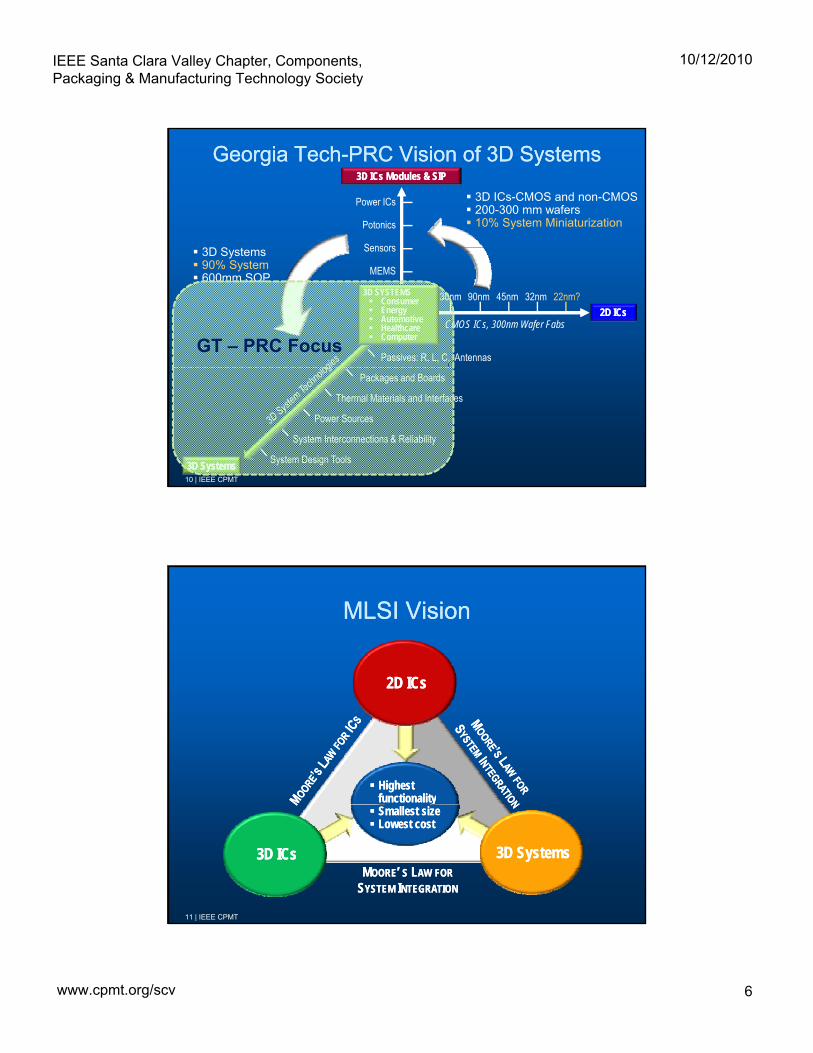
Power ICs
Potonics
Sensors
3D ICs 3D ICs Modules & SIPModules & SIP
3D ICs-CMOS and non-CMOS 200-300 mm wafers 10% System Miniaturization
3D S t
Georgia TechGeorgia Tech--PRC Vision of 3D SystemsPRC Vision of 3D Systems
Passives: R, L, C, Antennas
Sensors
MEMS
22nm?130nm
CMOS ICs, 300nm Wafer Fabs2D ICs2D ICs
90nm 45nm 32nm
3D Systems 90% System 600mm SOP
3D SYSTEMS Consumer Energy Automotive Healthcare Computer
GT – PRC Focus
Packages and Boards
Thermal Materials and Interfaces
Power Sources
System Interconnections & Reliability
System Design Tools3D Systems3D Systems10 | IEEE CPMT
MLSI VisionMLSI Vision
2D ICs2D ICs
•Functional Density• Miniaturized
Highest Highest functionalityfunctionality
2D ICs2D ICs
Miniaturized•Lower cost Smallest sizeSmallest size
Lowest costLowest cost
MMOOREOORE’ ’ SS LLAWAW FORFOR
SSYSTEMYSTEM IINTEGRATIONNTEGRATION
3D ICs3D ICs 3D Systems3D Systems
11 | IEEE CPMT

IEEE Santa Clara Valley Chapter, Components, Packaging & Manufacturing Technology Society
10/12/2010
www.cpmt.org/scv 7
Difference between SIP, SOP and 3D ICs Difference between SIP, SOP and 3D ICs
SIP Means SIP Means Stacked Stacked ICs and Packages (SIP)ICs and Packages (SIP)
SIP Stacked ICsSIP Stacked ICs SIP Stacked PackagesSIP Stacked Packages 3D ICs with TSV3D ICs with TSVSIP Stacked ICsSIP Stacked ICs 3D ICs with TSV3D ICs with TSV
2D and 3D ICs in MLSI2D and 3D ICs in MLSI
12 | IEEE CPMT
Moore’s Law for System Integration Moore’s Law for System Integration Vision @ GT PRCVision @ GT PRC
NANOMATERIALSEMBEDDED
COMPONENTSSUBSTRATES &
SYSTEM INTEGRATIONINTERCONNECTIONS
RDL
POWER
UltraUltra--Thin SiliconThin Silicon(30(30µm) with m) with TPVTPV
PD/TIALASER PHOTODETECTOR
Waveguide
OPTO SOP
NANOMAGNETICS
CHIP-LAST
EMBEDDED ICTHERMAL SOP
SYSTEM ON CHIP (SOC)
DIGITAL SOP ANALOG & RF SOP
GaAs RFIC
EBG &
Isolation
MEMS
MEMS PACKAGING
Bio-Sensor
SENSORS
CAPACITORS
ANTENNAS & FILTERS
13 | IEEE CPMT
HIGH DENSITY I/O 3D ICs
POWER& BATTERIES
MIXED SIGNAL ELECTRICAL DESIGN MECHANICAL DESIGN FOR RELIABILITYTHERMAL

IEEE Santa Clara Valley Chapter, Components, Packaging & Manufacturing Technology Society
10/12/2010
www.cpmt.org/scv 8
Grand Challenges in MLSIGrand Challenges in MLSI Moore’s Law in 2DMoore’s Law in 2D
•• ICs beyond 22 nm and with ULKICs beyond 22 nm and with ULK
•• Packaging of 2D ICsPackaging of 2D ICsPackaging of 2D ICsPackaging of 2D ICs
•• ProcessorProcessor--driven Thermal challengesdriven Thermal challenges
Moore’s Law in 3D Moore’s Law in 3D •• 3D ICs (with TSV) stack3D ICs (with TSV) stack
•• TSV, Interconnections, ThermalTSV, Interconnections, Thermal
•• Interposer Packaging Interposer Packaging
Moore’s Law for System IntegrationMoore’s Law for System Integration•• Thin film Passives: miniaturized and better propertiesThin film Passives: miniaturized and better propertiesThin film Passives: miniaturized and better propertiesThin film Passives: miniaturized and better properties
•• Interconnections: ChipInterconnections: Chip--level and Boardlevel and Board--levellevel
•• Thermal Technologies: MiniaturizationThermal Technologies: Miniaturization--drivendriven
•• Miniaturized and HighMiniaturized and High--Density BatteriesDensity Batteries
•• Miniaturized Packages and BoardsMiniaturized Packages and Boards
•• System Design ToolsSystem Design Tools
14 | IEEE CPMT
GrandparentGrandparent
There’s only one perfect grandchild in the worldThere’s only one perfect grandchild in the world Every grandparent has itEvery grandparent has it Every grandparent has itEvery grandparent has it
15 | City University of Hong Kong 2010

IEEE Santa Clara Valley Chapter, Components, Packaging & Manufacturing Technology Society
10/12/2010
www.cpmt.org/scv 9
Moore’s Law in 2DMoore’s Law in 2D
Challenges in 2DChallenges in 2D•• UltraUltra--low Power and yet ultralow Power and yet ultra--high Performancehigh Performanceyy gg•• ULK integrityULK integrity•• Si CMOS beyond 16nmSi CMOS beyond 16nm
PerformancePerformance
LeakageLeakage
16 | IEEE CPMT
Si CMOS beyond 16nmSi CMOS beyond 16nm FD SOI and Fin FETFD SOI and Fin FET
17 | IEEE CPMT
IEEE Santa Clara Valley Chapter, Components, Packaging & Manufacturing Technology Society
10/12/2010
www.cpmt.org/scv 10
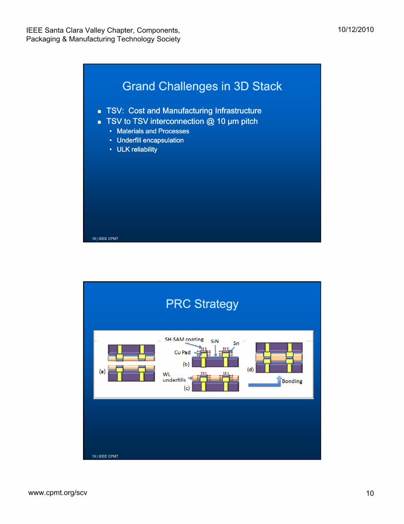
Grand Challenges in 3D Stack Grand Challenges in 3D Stack
TSV: Cost and Manufacturing InfrastructureTSV: Cost and Manufacturing Infrastructure TSV to TSV interconnection @ 10TSV to TSV interconnection @ 10 µmµm pitchpitch TSV to TSV interconnection @ 10 TSV to TSV interconnection @ 10 µm µm pitchpitch
•• Materials and ProcessesMaterials and Processes•• UnderfillUnderfill encapsulationencapsulation•• ULK reliabilityULK reliability
18 | IEEE CPMT
PRC StrategyPRC Strategy
19 | IEEE CPMT
IEEE Santa Clara Valley Chapter, Components, Packaging & Manufacturing Technology Society
10/12/2010
www.cpmt.org/scv 11
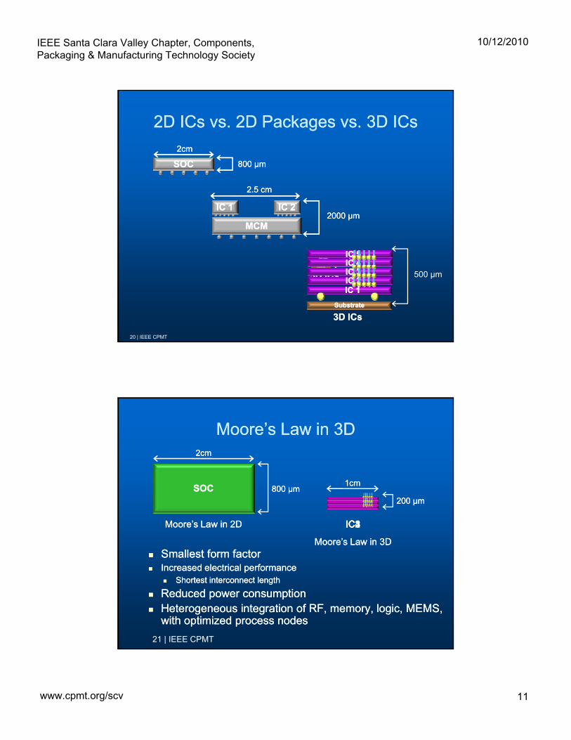
2D ICs vs. 2D Packages vs. 3D ICs2D ICs vs. 2D Packages vs. 3D ICs
SOCSOC
2cm
800 µmSOCSOC
2cm
800 µm
MCMMCM
2.5 cm
IC 2IC 2IC 1IC 12000 µm
IC 5IC 5IC 4IC 4
500IC 5IC 5
MCMMCM
2.5 cm
IC 2IC 2IC 1IC 12000 µm
IC 3IC 3IC 2IC 2IC 1IC 1
3D ICs3D ICs
500 µmSubstrateSubstrate
IC 4IC 4IC 3IC 3IC 2IC 2IC 1IC 1
3D ICs3D ICs
500 µm
SubstrateSubstrate
20 | IEEE CPMT
Moore’s Law in 3DMoore’s Law in 3D2cm2cm
11cmcmSOCSOCSOCSOC
Smallest form factor Smallest form factor I d l t i l fI d l t i l f
800 800 µmµm
Moore’s Law in 2DMoore’s Law in 2D
11cmcm
2200 00 µmµm
Moore’s Law in 3DMoore’s Law in 3D
IC4IC4IC3IC3IC2IC2IC1IC1
Increased electrical performanceIncreased electrical performance Shortest interconnect length Shortest interconnect length
Reduced power consumption Reduced power consumption Heterogeneous integration of RF, memory, logic, MEMS, Heterogeneous integration of RF, memory, logic, MEMS,
with optimized process nodeswith optimized process nodes
21 | IEEE CPMT

IEEE Santa Clara Valley Chapter, Components, Packaging & Manufacturing Technology Society
10/12/2010
www.cpmt.org/scv 12
3D IC Fundamentals 3D IC Fundamentals
5-15µm Underfill TSV for Signal
Fine Pitch Interconnections
Interposer
Embedded LCR
External InterfacePower Delivery
TSV for PowerTSV for Power
Source: Advanced Industrial Science and Technology (AIST)
Embedded LCR
10X Flip-chip Interconnections
High-speed Signal
Lower Power Dissipation
Low Cost
22 | IEEE CPMT
Past
Piggyback DIP: IBM, 1973
RecentChip Stack by Wirebonding: ChipPac
EmergingChip Stack by TSV: Bosch, TruSi etc.
3D Packaging & Integration Evolution3D Packaging & Integration Evolution
Stacked TSOP:
DST Modules, Inc.
POP + Chip Stack: Sharp
POP Ultra Thin W2W and D2W Stacking: IBM
Tohoku Univ, DARPA VISA, IMEC etc.
Si Thru Via ASET
,
POP + Chip-on-Chip: IMECUltra Thin RF modules by
EMAP by GT PRC
23 | IEEE CPMT

IEEE Santa Clara Valley Chapter, Components, Packaging & Manufacturing Technology Society
10/12/2010
www.cpmt.org/scv 13
3D Package Integration Evolution3D Package Integration Evolution
Flip-Chip or Wire Bond Wire Bond WLPPoP Edge Traces TSVEmbedded
M t M t E iM t E i E iE i
Source: Yole
Mature Mature EmergingMature Emerging EmergingEmerging
24 | IEEE CPMT
3D ICs begin with Memory Stack with TSV3D ICs begin with Memory Stack with TSV
Wire Bond Memory Stack TSV Memory Stack
Source: Nokia
eMMC memory package• 8 memories + 1 controller
25 | IEEE CPMT
IEEE Santa Clara Valley Chapter, Components, Packaging & Manufacturing Technology Society
10/12/2010
www.cpmt.org/scv 14
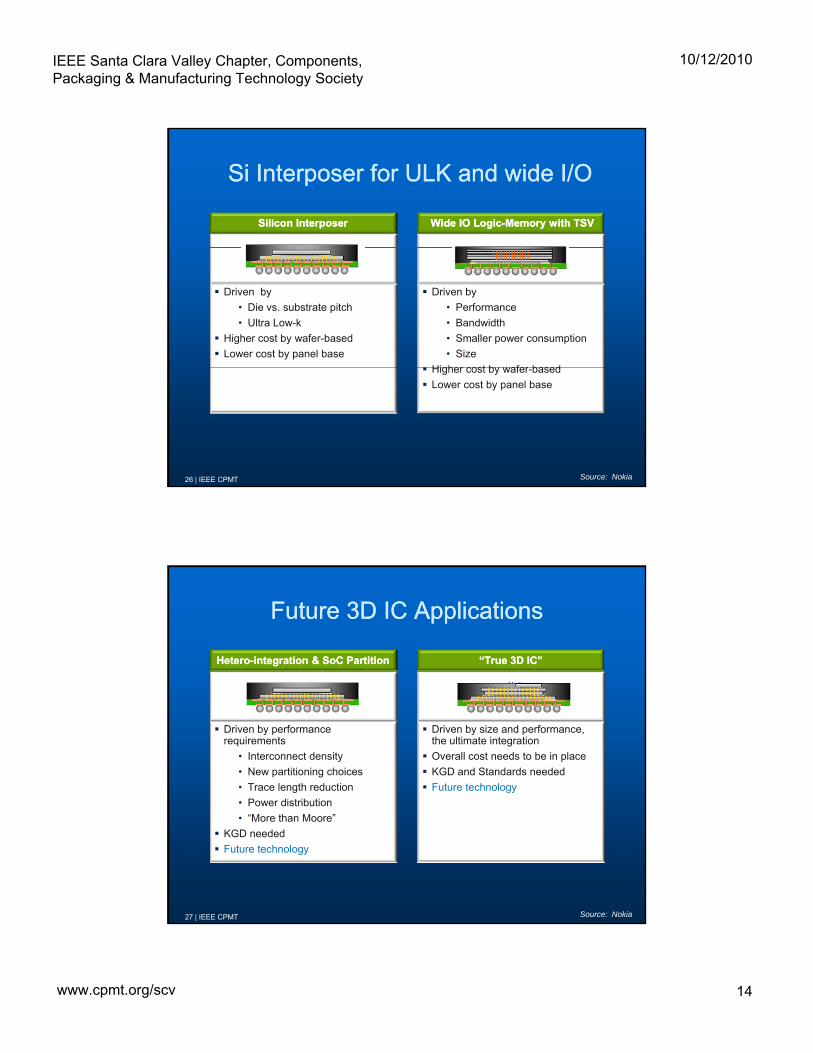
Si Interposer for ULK and wide I/O Si Interposer for ULK and wide I/O
Silicon InterposerSilicon Interposer Wide Wide IO LogicIO Logic--Memory with Memory with TSVTSV
Driven by
• Die vs. substrate pitch
• Ultra Low-k
Higher cost by wafer-based
Lower cost by panel base
Driven by
• Performance
• Bandwidth
• Smaller power consumption
• Size
Higher cost by wafer based Higher cost by wafer-based
Lower cost by panel base
Source: Nokia26 | IEEE CPMT
Future 3D IC ApplicationsFuture 3D IC Applications
HeteroHetero--integration & integration & SoCSoC Partition Partition “True 3D IC”“True 3D IC”
Driven by performance requirements
• Interconnect density
• New partitioning choices
• Trace length reduction
• Power distribution
Driven by size and performance, the ultimate integration
Overall cost needs to be in place
KGD and Standards needed
Future technology
Power distribution
• “More than Moore”
KGD needed
Future technology
Source: Nokia27 | IEEE CPMT

IEEE Santa Clara Valley Chapter, Components, Packaging & Manufacturing Technology Society
10/12/2010
www.cpmt.org/scv 15
Interposers for Packaging 3D ICsInterposers for Packaging 3D ICs ChallengesChallenges
•• High I/Os @ less than 30 um pitchHigh I/Os @ less than 30 um pitch•• Low cost/I/OLow cost/I/O
28 | IEEE CPMT
IC Package Technology Trend IC Package Technology Trend
Silicon &Silicon &
~2013~2013
Silicon & Silicon & Glass Glass
PackagesPackages
19701970
1990s1990s
OrganicsOrganicsWLPWLP1980s1980s
C iC i
LeadframeLeadframe
1970s1970s CeramicsCeramics
29 | IEEE CPMT

IEEE Santa Clara Valley Chapter, Components, Packaging & Manufacturing Technology Society
10/12/2010
www.cpmt.org/scv 16
CharacteristicCharacteristic WLPWLP InterposerInterposer
Large Wafer or Panel
WLP vs. PanelWLP vs. Panel--Based Interposer Based Interposer
Low-cost Facilities
Miniaturized Components Low-cost Materials and Processes High-throughout Tools
Smallest Package Size Thermal Performance
200-300 mm Wafer
WLPWLP
600 mm System-On-Panel
InterposerInterposer
30 | IEEE CPMT
10X
Ideal Properties of a Package MaterialIdeal Properties of a Package Material
CharacteristicIdeal Properties
Materials
Glass Silicon Plastic MetalElectrical High resistivityElectrical High resistivity
Low loss
Physical Smooth surface finish Large area availability Ultra thin
Thermal High Conductivity CTE matched to Si
Mechanical High strength High modulus
Chemical Resistance to process chemicals
Good Fair Poor
chemicals
Processability Ease of Via formation and metallization
Cost Low cost per I/O at 25um pitch
31 | IEEE CPMT

IEEE Santa Clara Valley Chapter, Components, Packaging & Manufacturing Technology Society
10/12/2010
www.cpmt.org/scv 17
Why PanelWhy Panel--based Glass & Si Packages?based Glass & Si Packages?
CeramicCeramic
Cost/I/O
PanelPanel--based based Glass & Si Glass & Si
OrganicOrganicSilicon Silicon
InterposerInterposer10x
I/O Pitch(um)
PackagesPackages
1x
225150
2D ICs2D ICs
50 100
3D ICs3D ICs
32 | IEEE CPMT
Multichip Multichip SaGISaGI Interposer ModuleInterposer Module
Large SiLarge Si--interposer and sizeinterposer and size
SaGI 30 – 100 µm
TPV
Micro Bump 30 – 60 µm ProcessorProcessor
O
RFRF MemoryMemory
C4 Bump
Source: Nokia
Organic Package
33 | IEEE CPMT
IEEE Santa Clara Valley Chapter, Components, Packaging & Manufacturing Technology Society
10/12/2010
www.cpmt.org/scv 18
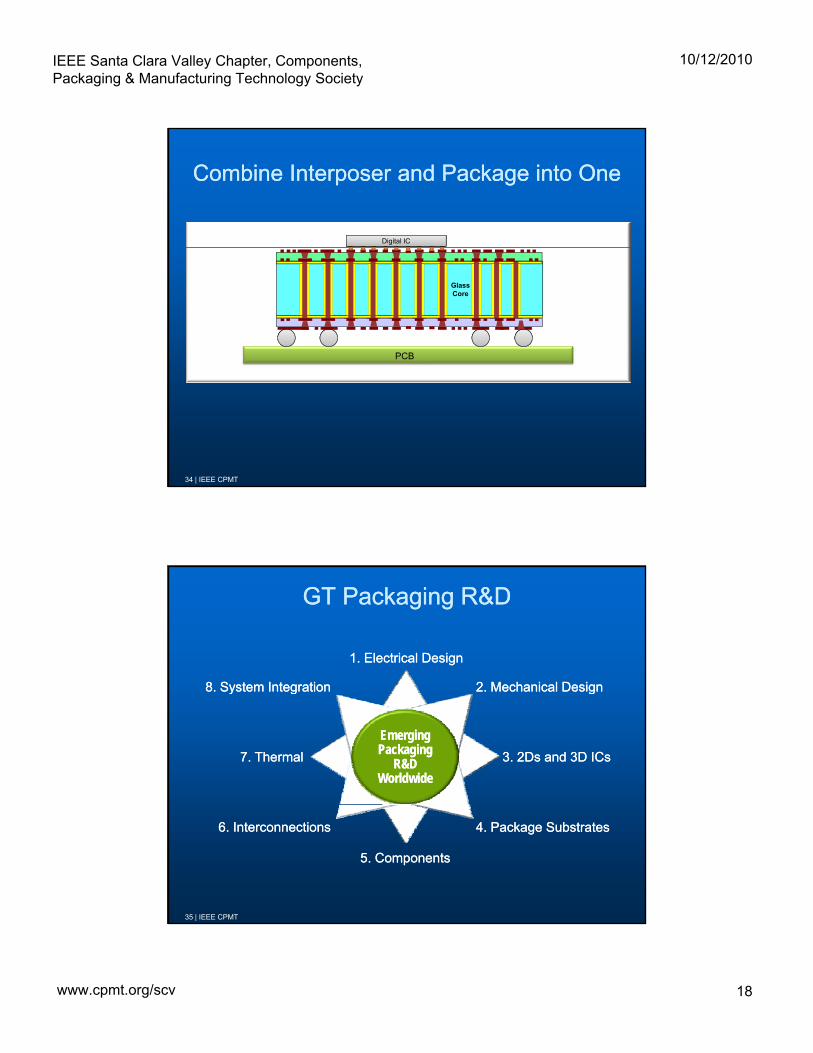
Combine Interposer and Package into OneCombine Interposer and Package into One
Digital IC
Glass Core
PCB
34 | IEEE CPMT
GT Packaging R&D GT Packaging R&D
1. Electrical Design1. Electrical Design
8 System Integration8 System Integration 2 Mechanical Design2 Mechanical Design
3. 2Ds and 3D ICs3. 2Ds and 3D ICs7. Thermal7. Thermal
8. System Integration8. System Integration 2. Mechanical Design2. Mechanical Design
Emerging Emerging Packaging Packaging
R&D R&D Worldwide Worldwide
5. Components5. Components
6. Interconnections6. Interconnections 4. Package Substrates4. Package Substrates
35 | IEEE CPMT

IEEE Santa Clara Valley Chapter, Components, Packaging & Manufacturing Technology Society
10/12/2010
www.cpmt.org/scv 19
Superiority of Glass Over SiliconSuperiority of Glass Over Silicon
TPV
30 µm30 µm
Silicon w/ Polymer or SiO2 LinerGlassEM Model
TPV100 µm
TPV100 µm
Glass
S21
(d
B)
Si 10ohm-cm, 0.1µm SiO2 liner
Si 10ohm-cm, 5µm polymer liner
36 | IEEE CPMT
Material Insertion Loss (dB) (@5.4GHz)
GLASS 0.74
Superiority of Glass Over SiliconSuperiority of Glass Over Silicon
3D View of a Filter
Si 1000 Ω-cm (High Resistivity) 2.02
Si 10 Ω-cm (Low Resistivity) 15.35
LL3R=
LL1R=
(dB)
Si 1000 Ω-cm
(High ResistivityGlass
Filter Schematic
CC2
CC1
CC4
CC5
LL5R=
LL4R=
CC3
Glass and Silicon Resistivity
Si 10 Ω-cm
(Low Resistivity)
S21
37 | IEEE CPMT
IEEE Santa Clara Valley Chapter, Components, Packaging & Manufacturing Technology Society
10/12/2010
www.cpmt.org/scv 20
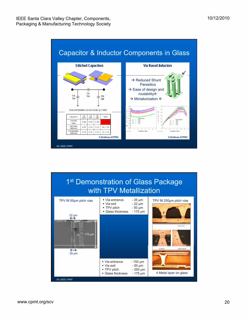
Capacitor & Inductor Components in GlassCapacitor & Inductor Components in Glass
Via Based InductorsStitched Capacitors
Reduced Shunt Parasitics
Ease of design and routability
Miniaturization
V.Sridhran,GTPRCV.Sridhran,GTPRC
38 | IEEE CPMT
TPV fill 250µm pitch vias Via entrance - 35 µm Via exit - 22 µm TPV pitch - 50 µm
TPV fill 50µm pitch vias
11stst Demonstration of Glass Package Demonstration of Glass Package with TPV Metallizationwith TPV Metallization
p µ Glass thickness - 175 µm
22 µm
175 µm
Via entrance - 150 µm Via exit - 50 µm TPV pitch - 250 µm Glass thickness - 175 µm 4 Metal layer on glass
35 µm
39 | IEEE CPMT

IEEE Santa Clara Valley Chapter, Components, Packaging & Manufacturing Technology Society
10/12/2010
www.cpmt.org/scv 21
Glass Substrate R&D ToGlass Substrate R&D To--datedate
Glass IPD (ST)
Photonic System-in-Package (IZM)
Glass Substrates (Longborough)
Glass Wafer (NEC Schott)y g ( )
3D Thin Film Interposer Based on TGV (IZM) Photosensitive Glass (Life Bioscience)
( )
40 | IEEE CPMT
Through Package Via in GlassThrough Package Via in Glass
Mechanical Drilling in 200mm Glass (GT PRC)
Photosensitive Glass (Life Bioscience) Laser Ablation (GT PRC)( )
Schott Glass (NEC-Schott)
( )
41 | IEEE CPMT
Chemical (Natl Inst R&D of Microelectronics)

IEEE Santa Clara Valley Chapter, Components, Packaging & Manufacturing Technology Society
10/12/2010
www.cpmt.org/scv 22
Miniaturized BoardsMiniaturized Boards Converge Packages and Boards into Converge Packages and Boards into
Miniaturized System PackagesMiniaturized System Packages Develop Micro SMTDevelop Micro SMT
42 | IEEE CPMT
MLSI Must Eliminate the GapMLSI Must Eliminate the Gap
250,000
200 000
IC
ICSYSTEM
Gap ~ 105 x
20,000
4,000raph
ic D
imen
sion
(nm
)
200,000
100,000125,000nm
System ona Package
ICPACKAGEGap ~ 104
1980 1990 2010 202019700
2,000Lith
og
32nm
3,200nm1,000nm
43 | IEEE CPMT
IEEE Santa Clara Valley Chapter, Components, Packaging & Manufacturing Technology Society
10/12/2010
www.cpmt.org/scv 23
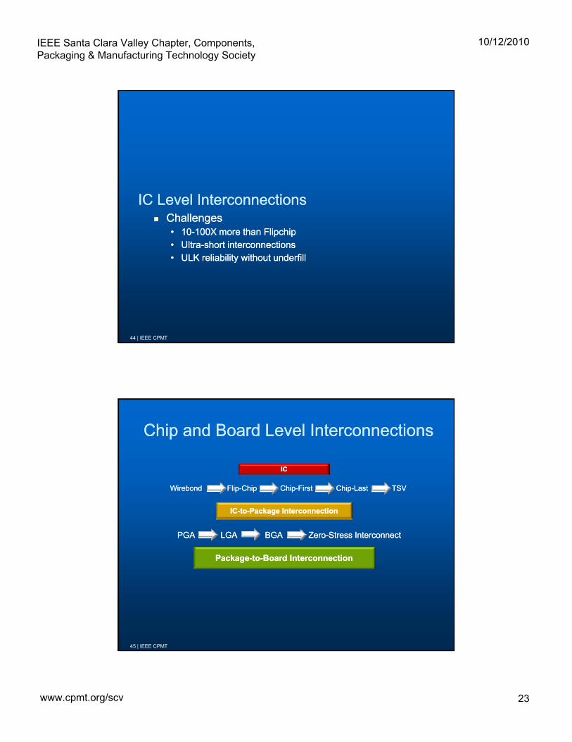
IC Level InterconnectionsIC Level Interconnections ChallengesChallenges
•• 1010--100X more than 100X more than FlipchipFlipchip•• UltraUltra--short interconnectionsshort interconnections•• ULK reliability withoutULK reliability without underfillunderfillULK reliability without ULK reliability without underfillunderfill
44 | IEEE CPMT
Chip and Board Level Interconnections Chip and Board Level Interconnections
ICIC
PackagePackage--toto--Board InterconnectionBoard Interconnection
ICIC--toto--Package Interconnection Package Interconnection
WirebondWirebond FlipFlip--ChipChip ChipChip--FirstFirst ChipChip--LastLast TSVTSV
PGAPGA LGALGA BGABGA ZeroZero--Stress InterconnectStress Interconnect
45 | IEEE CPMT

IEEE Santa Clara Valley Chapter, Components, Packaging & Manufacturing Technology Society
10/12/2010
www.cpmt.org/scv 24
Why Embedding?Why Embedding?
I/O Density/mmI/O Density/mm33
•• Wire BondWire Bond Flip ChipFlip Chip 10X Flip Chip10X Flip Chip 100X Flip Chip100X Flip Chip
Functional Density/mmFunctional Density/mm33
•• Smart Phone FunctionalitySmart Phone Functionality
Heterogeneous Integration Density/mmHeterogeneous Integration Density/mm33
•• Digital CMOSDigital CMOS
p pp p p pp p p pp p
MegaMega--functionalityfunctionality
RF, Optical, Analog, SensorRF, Optical, Analog, Sensor
46 | IEEE CPMT
Embedded Strategy for I/O DensityEmbedded Strategy for I/O Density
HVM - FlipFlip--ChipChip
4X
WirebondWirebond
1X
10X
Tech
no
log
y M
atu
rity
LVM -
Organic Package• Flex• Molded
10x flip chip
New Infrastructure New Business
Model
FlipFlip ChipChipWirebondWirebond
IC
ChipChip--First ICFirst IC
ChipChip--LastLastand Subsystemand Subsystem
I/O Density (per chip area)1x ~4x ~10-40x
T R&D - 10x flip chip Reworkable
• Existing Infrastructure• Heterogeneous
Integration10X
47 | IEEE CPMT

IEEE Santa Clara Valley Chapter, Components, Packaging & Manufacturing Technology Society
10/12/2010
www.cpmt.org/scv 25
Embedded Actives in R&D & ManufacturingEmbedded Actives in R&D & Manufacturingve
s
Supply Supply ChainChain
I fiI fi
GT PRCGT PRCChip-Last Embedded Actives & Passives
on
of
Em
bed
ded
Act
iv
ShinkoShinko
DaeduckDaeduck, , AT&S, AT&S, IbidenIbiden
ASE, ASE, STATS (eSTATS (e--
WLB)WLB)
BBUL BBUL Chip First
CasioCasioe-WLP
ImberaImbera, , AT&S, AT&S, IbidenIbiden
Embedded Die in Substrate
Infineon, Infineon, FreescaleFreescaleWafer-Level Fan Out
11stst Patent Patent (Philips)(Philips)
Evo
luti
o
1970 20001990 2010
(Intel)(Intel)Chip-First
11stst
Prototype Prototype (MIT, GE)(MIT, GE)
48 | IEEE CPMT
Subsystem Embedding with ChipSubsystem Embedding with Chip--Last @ GT PRCLast @ GT PRC
RF/MEMSRF/MEMS IPDIPD3DIC3DIC
CORE
DIGITALDIGITAL
1.1. Embedded MEMS, Activies and Passives (EMAP)Embedded MEMS, Activies and Passives (EMAP)2.2. 9X higher I/O density than flip chip9X higher I/O density than flip chip3.3. Subsystem embeddingSubsystem embedding4.4. ULK compatible ULK compatible 5.5. Existing manufacturing infrastructureExisting manufacturing infrastructure6.6. Compatibility with activies, MEMS, and power componentsCompatibility with activies, MEMS, and power components
49 | IEEE CPMT

IEEE Santa Clara Valley Chapter, Components, Packaging & Manufacturing Technology Society
10/12/2010
www.cpmt.org/scv 26
Two Approaches to Embedded ActivesTwo Approaches to Embedded Actives
Schematic
FlipFlip--ChipChip ChipChip--FirstFirst ChipChip--Last @ GT PRCLast @ GT PRC
Substrate
Interconnect Pitch Stand-off
Assembly
Testability
Laminate
C4 100-150µm 50-80µm
Solder reflow
Known good die and substrate
Carrier / Mold / Tape
RDL via 40-80µm 3-10µm
RDL process
Known good die and known good package challenges
Laminate
Cu-Cu bonding 30-50µm 5-15µm
Thermocompression
Known good die and substrate
Reworkability
Manufacturing Infrastructure
Wirebond die
MEMS Integration
Yes
Existing
Needs redistribution
No cavity, surface only
g
Challenge
New infrastructure
Can be used as is
Challenge
Yes
Existing
Can be used as is
Cavity readily allows
50 | IEEE CPMT
9X Flip9X Flip--chip with 2000 Cycle Reliabilitychip with 2000 Cycle Reliability
Ultra Thin Low CTE & Low Loss Organic Substrate
High Isolation for Embedded Actives using EBGs
High-Q Embedded Filters
Ultra-Thin, Low CTE & Low Loss Organic Substrate
Fine Pitch I/O Wiring with High Reliability
25µm
Embedded Die Reliability Demonstration
High-Q Embedded Filters
Precise Laser Cavity for Ultra-Fine Pitch IC Embedding
High Reliability Cu Microbump Interconnect at 30µm Pitch & 10µm Height
51 | IEEE CPMT

IEEE Santa Clara Valley Chapter, Components, Packaging & Manufacturing Technology Society
10/12/2010
www.cpmt.org/scv 27
Subsystem Embedding with ChipSubsystem Embedding with Chip--Last @ GT PRCLast @ GT PRC
RF/MEMSRF/MEMS IPDIPD3DIC3DIC
SaGI( Silicon or Glass)
DIGITALDIGITAL
1.1. Embedded MEMS, Activies and Passives (EMAP)Embedded MEMS, Activies and Passives (EMAP)2.2. 9X higher I/O density than flip chip9X higher I/O density than flip chip3.3. Subsystem embeddingSubsystem embedding4.4. ULK compatible ULK compatible 5.5. Existing manufacturing infrastructureExisting manufacturing infrastructure6.6. Compatibility with activies, MEMS, and power componentsCompatibility with activies, MEMS, and power components
52 | IEEE CPMT
Recent R&D at PRCRecent R&D at PRC
100 µm pitch lead-free flip-chip reliability
With Underfill Without Underfill
Nano Interconnections
30um pitch chip-last interconnectionsNano-Cu I/Os at 50um pitch G-Helix compliant interconnections
53 | IEEE CPMT

IEEE Santa Clara Valley Chapter, Components, Packaging & Manufacturing Technology Society
10/12/2010
www.cpmt.org/scv 28
BoardBoard--Level Interconnection Level Interconnection ChallengesChallenges
ChallengesChallenges•• SMT Pitch 400m, single biggest barrier to MLSISMT Pitch 400m, single biggest barrier to MLSI, g gg, g gg•• Two OptionsTwo Options
Converge Package and BoardConverge Package and Board
Reduce pitch toReduce pitch to 200m200m 100m100m 50m50m
54 | IEEE CPMT
Thermal Thermal
ChallengesChallenges•• SOC or 2D LevelSOC or 2D Level
ULP devicesULP devices
NanoNano thermal interfacesthermal interfaces
•• 3D IC Level3D IC Level MicrofluidicsMicrofluidics for high power applicationsfor high power applications
HighHigh-- K Interposers for consumer applicationsK Interposers for consumer applications
•• System levelSystem level ULP devicesULP devices ULP devicesULP devices
55 | IEEE CPMT

IEEE Santa Clara Valley Chapter, Components, Packaging & Manufacturing Technology Society
10/12/2010
www.cpmt.org/scv 29
Thermal ManagementThermal Management
Hand-Held Up to 60 W/cm2 locally TIM, Heat slugs and Heat Spreaders
Automotive 250 W/cm2 projected Reliability at 100-2000C
Cost-Performance 20-50 W/cm2 at local hot spots Cost constraints limit to air cooling
High-Performance: 100-150 W/cm2
Fluidic Cooling
56 | IEEE CPMT
Thermal Interface MaterialsThermal Interface Materials
BLT m
Heat
spreader
Heat
spreader TIM1
TIM2
10
50
250
BLT m
Thermal grease
Nanocomposite
Indium
W/mK5001 100
p
57 | IEEE CPMT

IEEE Santa Clara Valley Chapter, Components, Packaging & Manufacturing Technology Society
10/12/2010
www.cpmt.org/scv 30
CNTs as TIMCNTs as TIMSolderSolder--assisted CNT Transferassisted CNT Transfer
SiSi
CNT Transferflip transferflip transfer
Grow on siliconGrow on silicon Aligned CNT bundlesAligned CNT bundles
SiSi
Solder
CopperCopper
Source: C P Wong, GT - PRC
C.P. Wong, L. Zhu(U.S.Patent-pending)
Solder
CopperCopper
Reflow and remove SiReflow and remove Si
58 | IEEE CPMT
Thin film PassivesThin film Passives
From NMDC 2From NMDC 2--4 slides4 slides
59 | IEEE CPMT

IEEE Santa Clara Valley Chapter, Components, Packaging & Manufacturing Technology Society
10/12/2010
www.cpmt.org/scv 31
Miniaturized & High Storage BatteriesMiniaturized & High Storage Batteries
60 | IEEE CPMT
Packaging Materials: Packaging Materials: Yesterday and TomorrowYesterday and Tomorrow
MaterialsMaterials CurrentCurrent FutureFuture
Battery
Nano porous silicon forsuper-charged Li batteries
Cylindrical Lithium-ion Battery Lithium Titanium Oxide arrays
61 | IEEE CPMT

IEEE Santa Clara Valley Chapter, Components, Packaging & Manufacturing Technology Society
10/12/2010
www.cpmt.org/scv 32
MLSI Electrical ChallengesMLSI Electrical Challenges
Glass and Glass and Silicon Silicon
Signal and Signal and Power Power
PackagePackage
Embedded Embedded Passive Passive DesignDesign
IntegrityIntegrity
ElectricalElectrical
TPV DesignTPV Design
ChallengesChallenges
InterconnectionInterconnectionDesignDesign
Mixed Signal Mixed Signal Design and Design and
ToolsTools
62 | IEEE CPMT
MLSI Mechanical ChallengesMLSI Mechanical Challenges
SystemSystem--Design forDesign forReliability withReliability with
ChipChip--PackagePackage--System System
DesignDesign--forfor--Reliability of Reliability of
Individual Failure Individual Failure MechanismsMechanisms
++Material Length ScaleMaterial Length ScaleEffects in MechanicalEffects in Mechanical
Design & ModelingDesign & Modeling
ChipChip PackagePackage System System InteractionInteraction++
Package & Package & System EvolutionSystem Evolution
Reduced Feature Size Increased Integration
63 | IEEE CPMT
IEEE Santa Clara Valley Chapter, Components, Packaging & Manufacturing Technology Society
10/12/2010
www.cpmt.org/scv 33
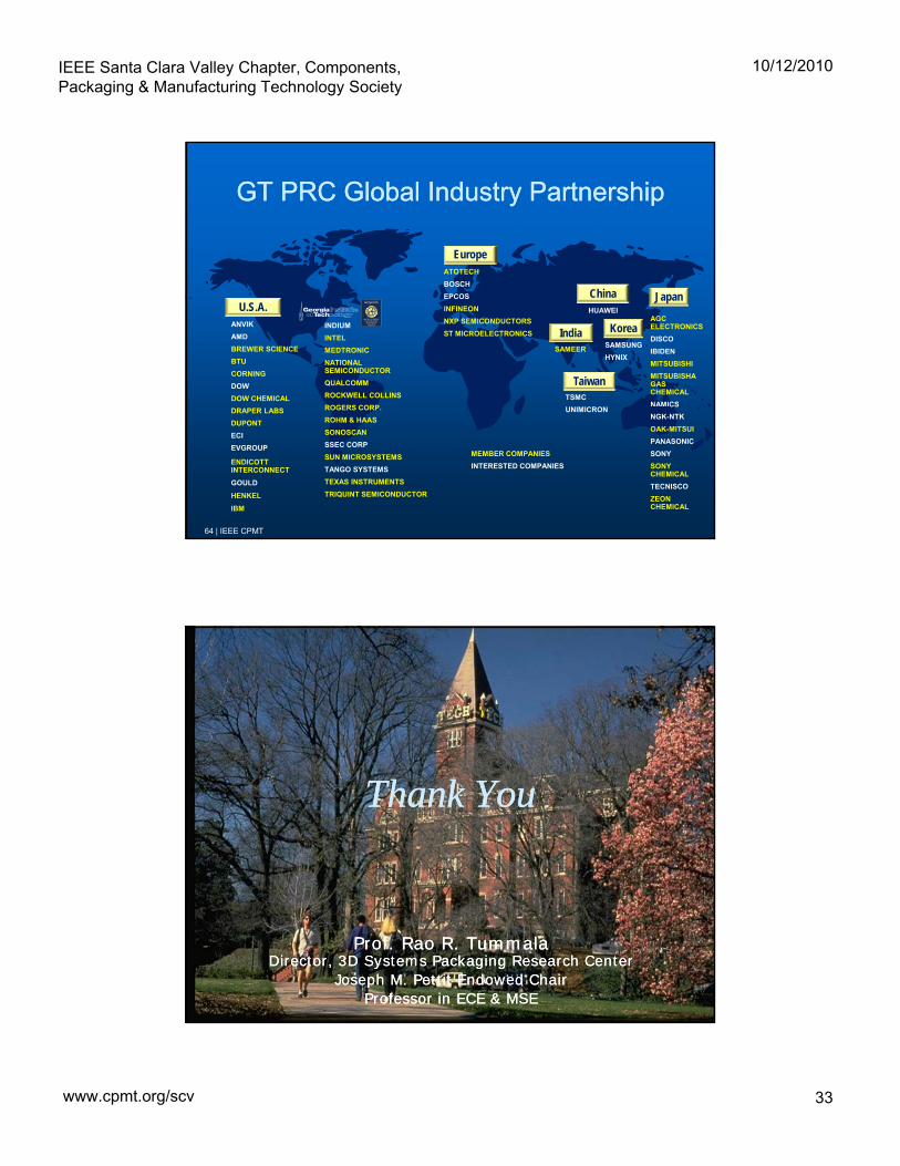
GT PRC Global Industry Partnership GT PRC Global Industry Partnership
EuropeATOTECHATOTECH
BOSCH
EPCOS
INFINEON
NXP SEMICONDUCTORS
ST MICROELECTRONICS IndiaSAMEER
KoreaSAMSUNG
HYNIX
Japan
AGC ELECTRONICS
DISCO
IBIDEN
MITSUBISHI
MITSUBISHA GAS CHEMICAL
NAMICS
U.S.A.ANVIK
AMD
BREWER SCIENCE
BTU
CORNING
DOW
DOW CHEMICAL
INDIUM
INTEL
MEDTRONIC
NATIONAL SEMICONDUCTOR
QUALCOMM
ROCKWELL COLLINS
ROGERS CORP
TaiwanTSMC
ChinaHUAWEI
CS
NGK-NTK
OAK-MITSUI
PANASONIC
SONY
SONY CHEMICAL
TECNISCO
ZEON CHEMICAL
DRAPER LABS
DUPONT
ECI
EVGROUP
ENDICOTT INTERCONNECT
GOULD
HENKEL
IBM
ROGERS CORP.
ROHM & HAAS
SONOSCAN
SSEC CORP
SUN MICROSYSTEMS
TANGO SYSTEMS
TEXAS INSTRUMENTS
TRIQUINT SEMICONDUCTOR
UNIMICRON
MEMBER COMPANIES
INTERESTED COMPANIES
64 | IEEE CPMT
Thank YouThank You
Prof. Prof. RaoRao R. TummalaR. TummalaDirector, 3D Systems Packaging Research CenterDirector, 3D Systems Packaging Research Center
Joseph M. Pettit Endowed Chair Joseph M. Pettit Endowed Chair Professor in ECE & MSEProfessor in ECE & MSE