grounding: the grounds for emc design grounding: the ...emc27.elfak.ni.ac.rs/downloads/grounding...
TRANSCRIPT

Grounding: The Grounds for EMC Design
1
Grounding: The Grounds for EMC Design
Elya B. JoffePresident, IEEE PSE SocietyPast President, IEEE EMC Society
Grounding: The Grounds for EMC Design
"Ground is where potatoes and carrots thrive"
(Dr. Bruce Archambeault)

Grounding: The Grounds for EMC Design
2
Grounding in EMC Engineering
• “Grounding” is probably of electrical/electronic systemdesign, often considered as "black magic“
Not easy to understand intuitively
No straightforward definition, modeling or analysis
Many uncontrolled factors affect its performance
• Grounding forms an inseparable part of all electronic andelectrical designs, from circuit through system up toinstallation design
Implemented for EMC and ESD protection, for safety purposes, for lightning and surge protection, etc.

Grounding: The Grounds for EMC Design
3
Parasitics in Passive Circuit Elements
Parasite – An organism that grows, feeds, andis sheltered on or in a different organismwhile contributing nothing to the survival of itshost

Grounding: The Grounds for EMC Design
4
“Real World” Resistors
RLS
CP
1
1R S
P
Z j L
j CR
ωω
= + +
Frequency response of "Real World" (non-ideal) Resistors, (R=10ΩΩΩΩ, LS=50nH and CP=1nF)
0
2
4
6
8
10
12
1 10 100
Frequency [MHz]
Imp
ed
an
ce [
Oh
m]

Grounding: The Grounds for EMC Design
5
“Real World” Capacitors
C RS
(ESR)LS
(ESL)
Rp
1
1C S S
P
Z j L R
j CR
ωω
= + +
+
Frequency response of "Real World" (non-ideal) Capacitors, (C=10nF, LS=5nH and RS=2mΩΩΩΩ)
0.01
0.1
1
10
100
1 10 100
Frequency [MHz]
Imp
ed
an
ce [
Oh
ms]

Grounding: The Grounds for EMC Design
6
“Real World” Inductors
RSL
Rp
Cp
1
1 1L
P
P S
Z
j CR j L R
ωω
=+ +
+
Frequency response of "Real World" (non-ideal) Inductors, (L=1µµµµH, R=10mΩΩΩΩ and CP=10pF)
10
100
1000
10000
10 100Frequency [MHz]
Imp
ed
an
ce [
Oh
ms
]

Grounding: The Grounds for EMC Design
7
Conclusions: “The Invisible Circuit”• Nothing is like it seems at first…
At high frequencies, where performance of reactive components is most needed (e.g., for filters) - they may not perform as anticipated
The INVISIBLE CIRCUIT must be considered in hi-speed circuit design

Grounding: The Grounds for EMC Design
8
Common Mode and Differential Mode Signals
Grounding: The Grounds for EMC Design
9
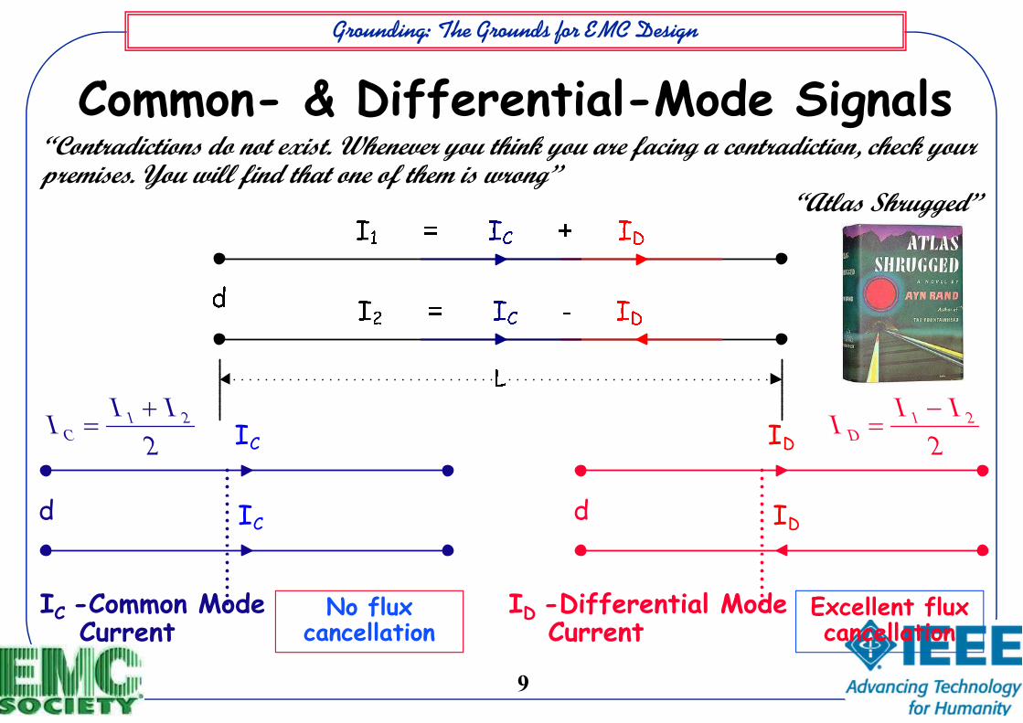
Common- & Differential-Mode Signals
II I
C=
+1 2
2I
I I
D=
−1 2
2ID
IDd
IC
ICd
ID -Differential ModeCurrent
IC -Common ModeCurrent
Excellent flux cancellation
No flux cancellation
“Contradictions do not exist. Whenever you think you are facing a contradiction, check your premises. You will find that one of them is wrong”
“Atlas Shrugged”

Grounding: The Grounds for EMC Design
10
Sources of Common-Mode Signals
“Ground Loops” External Radiated Field
Or Capacitive Crosstalk
Electric Flux
Dr
Vin
-2 ICM
VG
+IDM
+ICM
-IDM
+ICMA
I1
I2
I3

Grounding: The Grounds for EMC Design
11
Signal Propagation:“Path of Least Impedance” Principle
Fermat's principle leads to Snell's law; when the sines of the angles in the different media are in the same proportion as the propagation velocities, the time to
get from P to Q is minimized.
Hikers choose the easy way to cross hills
In thermodynamics, the enthalpy or heat content is a quotient or description of thermodynamic potential of a system, which can be used to calculate the "useful" work obtainable from a closed thermodynamic system under constant pressure and entropy.

Grounding: The Grounds for EMC Design
12
One Rule to bring them alland in the darkness bind them....
One Ring to rule them all,One Ring to find them,
One Ring to bring them alland in the darkness bind them....
Grounding: The Grounds for EMC Design
13
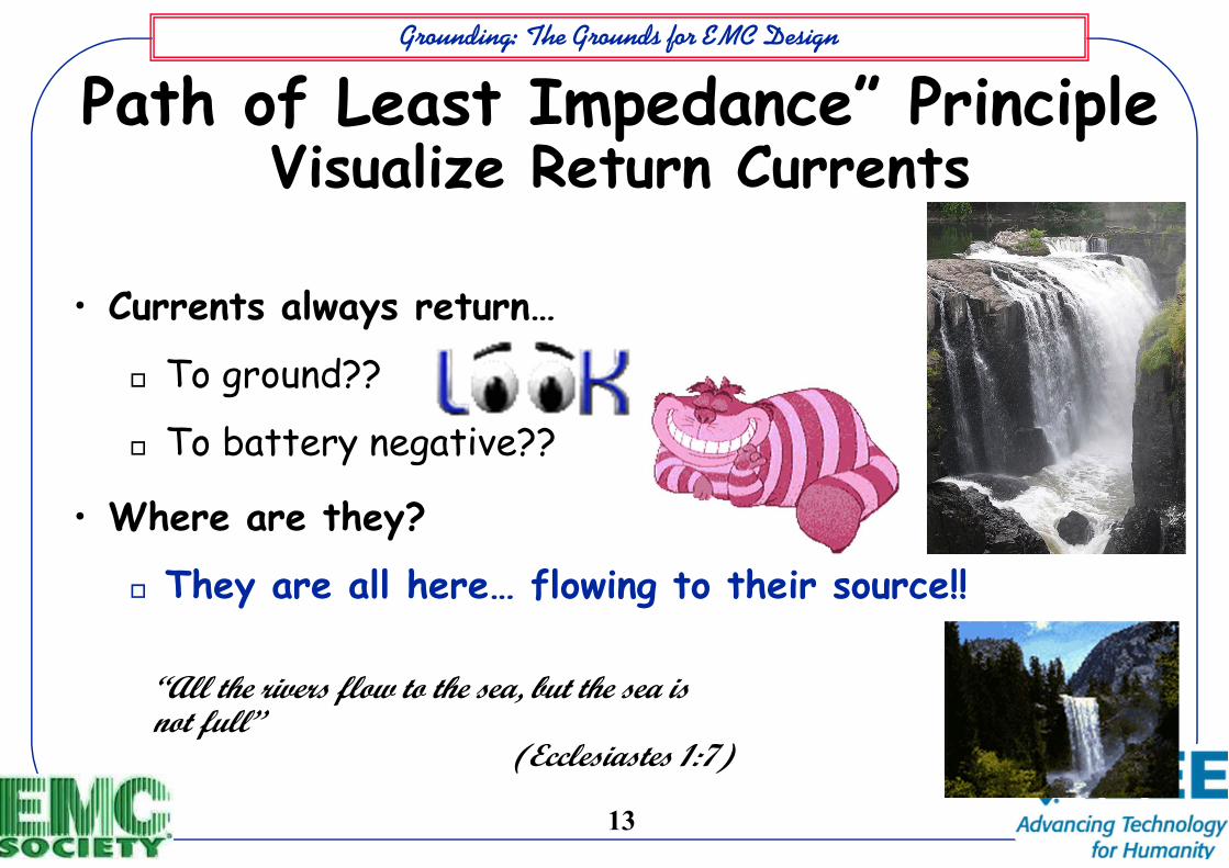
Path of Least Impedance” Principle Visualize Return Currents
• Currents always return…
To ground??
To battery negative??
• Where are they?
They are all here… flowing to their source!!
“All the rivers flow to the sea, but the sea is not full”
(Ecclesiastes 1:7)
Grounding: The Grounds for EMC Design
14
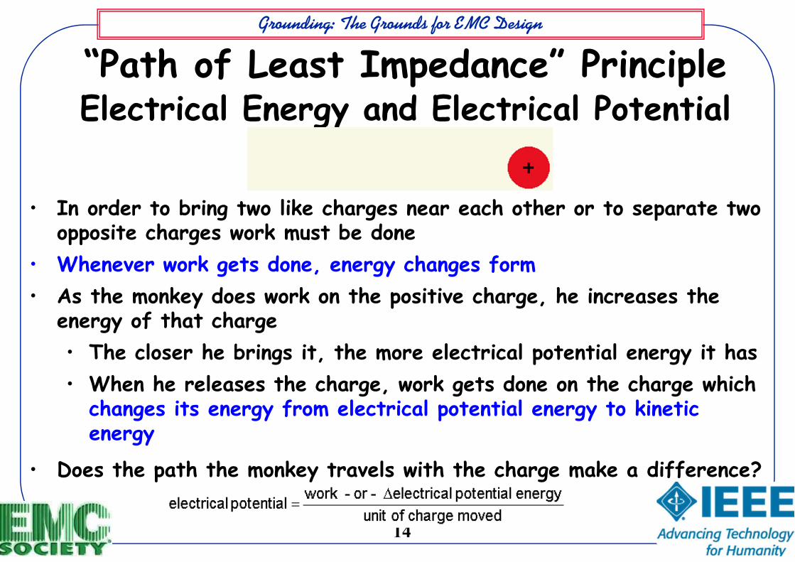
“Path of Least Impedance” PrincipleElectrical Energy and Electrical Potential
• In order to bring two like charges near each other or to separate two opposite charges work must be done
• Whenever work gets done, energy changes form
• As the monkey does work on the positive charge, he increases the energy of that charge
• The closer he brings it, the more electrical potential energy it has
• When he releases the charge, work gets done on the charge which changes its energy from electrical potential energy to kinetic energy
• Does the path the monkey travels with the charge make a difference?

Grounding: The Grounds for EMC Design
15
• Work done against an electric force in carrying a charge along a path from point a to b
• Electric Potential between with the points a and b:
b b b
a a a
W F dl qE dl q E dl= − • = − • = − •∫ ∫ ∫
( )work,or Δelectric-energy
charge moved
b
E a b
a
WV E dl
q→∆ = − • = =∫
Fur
dluur
dluur
a b b aW W→ →= −
“Path of Least Impedance” PrincipleElectrical Energy and Electrical Potential
• Does the path the monkey travels with the charge make any difference? Around a closed loop?
( ) ( ) 0
b
b aE a b E a b a
a
V E dl V V V→ → →∆ = − • = − ⇒ ∆ ≡∫ Right?
In a lossless medium…

Grounding: The Grounds for EMC Design
16
• When time-varying magnetic fields are present it is not possible to describe the electric field simply in terms of a scalar potential V because the electric field is no longer conservative
• is path-dependent because: ∇∇∇∇×E≠0 (Faraday's law of induction)
“Path of Least Impedance” PrincipleElectrical Energy and Electrical Potential
• In such cases we must consider the magnetic (vector) potential as well, and:
• Which remains conservative
C
E dl•∫
Wrong!!!
AE V
t
∂= −∇ −
∂
ur
In a lossless medium…
EFur
dluur
dluur
a b b aW W→ →= −
MFur
b
b a
a
E dl V V− • ≠ −∫

Grounding: The Grounds for EMC Design
17
“Path of Least Impedance” PrincipleWhich Path will the Return Current follow?
• Currents always take the path of least … Distance? Resistance? Impedance!!!

Grounding: The Grounds for EMC Design
18
Equivalent Circuit
“Path of Least Impedance” Principle Which Path will the Return Current follow?
or:-
1( ) 0S S SI R j L I j Mω ω⋅ + − ⋅ =
SL M=
1
S S
S S
I j L
I R j L
ωω
=+
1 1, Sg S
S
RI I I I
Lω<< → ⇔ >>
SS g
S
RI I
Lω>> ⇔ >>
In ”tightly coupled” conductors:
1C
21Br
2S
d sr
1I11Br
2C
12 12
dIV L
dt=

Grounding: The Grounds for EMC Design
19
“Path of Least Impedance” Principle Which Path will the Return Current follow?
2 1
1 2
VsI Z
Z Z= ⋅
+1 2
1 2
VsI Z
Z Z= ⋅
+
1 2 2 1
1 1
1 1 1 1 1 1
1 1 1 1
If Z >>Z I >>I (Ohm's Law)
min min
If Z , minZ minR +jX
If R << X minZ min X
I Z
R jX
→
→
= + →
→ ↔
The Second law of Thermodynamics: In a system, a process that occurs will tend to increase the total entropy
of the universe.

Grounding: The Grounds for EMC Design
20
“Path of Least Impedance” PrincipleWhich Path will the Return Current follow?
• At LOW FREQUENCIES, the current will follow the path of LEASTRESISTANCE, via ground (IG)
1 /
S
S S
jI I
R L j
ωω
= ⋅+
0
| | @
| | @ S S S
S
S S S
Z R R jZ R j M
Z L L R
Lω
ωω
ωω
→ = + ⋅ =
≈ ⋅ ⋅ >>
≈ >> ⋅
M
Source Cable Load
RS
LS RL
Ig
I1
IS
Grounding: The Grounds for EMC Design
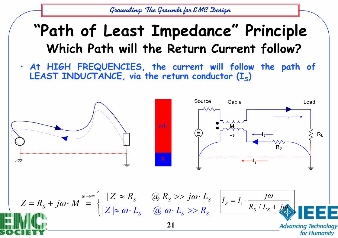
21
• At HIGH FREQUENCIES, the current will follow the path ofLEAST INDUCTANCE, via the return conductor (IS)
| | @
|
| @ S S S
S S
S
S
Z R R j
Z L LM
R
LZ R j
ω
ω ωω
ω→∞
≈ ⋅ ⋅ >>
≈ >> ⋅= + ⋅ =
“Path of Least Impedance” PrincipleWhich Path will the Return Current follow?
1 /
S
S S
jI I
R L j
ωω
= ⋅+

Grounding: The Grounds for EMC Design
22
“Path of Least Impedance” Principle Experiment Set-Up

Grounding: The Grounds for EMC Design
23
“Path of Least Impedance” PrincipleWhen is Inductance Minimized?
• Where is Inductance minimized?
• Same circumference, differentareas…
A
B da
LI I
φ⋅
= ≈∫ur r
,B Φ
Current I
X X X X X
X X X X X
X X X X X

Grounding: The Grounds for EMC Design
24
“Path of Least Impedance” PrincipleWhen is Inductance Minimized?
• Definition of Total Loop Inductance
• For I=constant, F min implies A min
( ) min min min, ...
A
B da
LI I
B B I thus L A
φ
φ
⋅
= ≈
= ⇒ ⇒
∫ur r
ur ur
,B Φ
Current I
LI
Φ=
Grounding: The Grounds for EMC Design
25
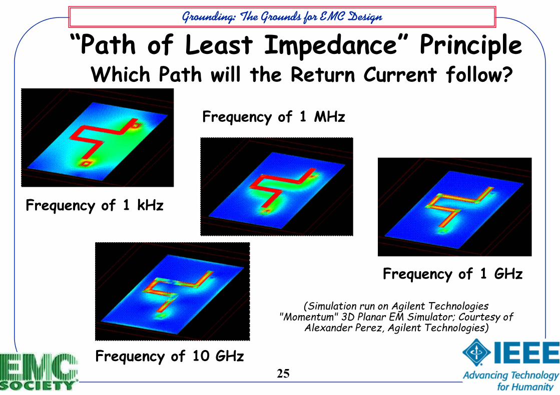
“Path of Least Impedance” Principle Which Path will the Return Current follow?
Frequency of 1 kHz
Frequency of 1 MHz
(Simulation run on Agilent Technologies "Momentum" 3D Planar EM Simulator; Courtesy of
Alexander Perez, Agilent Technologies)
Frequency of 1 GHz
Frequency of 10 GHz
Grounding: The Grounds for EMC Design
26
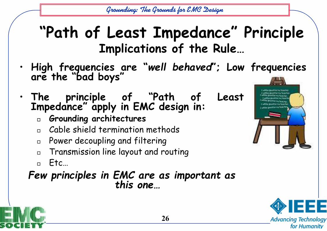
• High frequencies are “well behaved”; Low frequenciesare the “bad boys”
“Path of Least Impedance” Principle Implications of the Rule…
• The principle of “Path of LeastImpedance” apply in EMC design in:
Grounding architectures Cable shield termination methods Power decoupling and filtering Transmission line layout and routing Etc…
Few principles in EMC are as important as this one…

Grounding: The Grounds for EMC Design
27
Grounding Essentials, or… The Grounds for Grounding

Grounding: The Grounds for EMC Design
28
Purposes for Grounding
• Safety: Prevention of shock hazard to personnel Due to lightning strokes or power line short circuits to enclosure
• Path for return current (e.g., aircraft) Vehicle/platform/structure serves as return conductor
•EMC

Grounding: The Grounds for EMC Design
29
• AC power distribution is governed by national codes• One requirement: With each outgoing phase and neutral wire there
must be a safety ground
Rational for GroundingElectrical Shock Hazards
230V
Phase
0V
Neutral
to Return Ground
230V
Phase
0V
Neutral
to Safety GND
Equipment Enclosure Equipment EnclosureAccidental
Short
Accidental
Short
GND @
Service
EntryGND @
Service
Entry
No Safety Ground: Hazard Safety Ground Protection: SafeThe safety ground shunts the fault currents to the power return,
bypassing (and saving) the person
230230
1,0!!!
00L
B
V VI mA
R≈ ≅ =
Ω

Grounding: The Grounds for EMC Design
30
Ground Coupled interference
"Grounding Systems are Interference
Distribution Devices"
(Dr. Carl E. Baum)

Grounding: The Grounds for EMC Design
31
The Grounding ProblemLightning Hazards
Control CenterFuel Tank
External Lightning Protection System
Good Grounding
Surge propagating on Data Lines
Ungrounded cable penetration the
facility50 kV
The ungrounded cable penetrating the fuel tank, caused a potentialdifference between the cable and the facility’s structure, and thus- caused its explosion
50 kA
Good Grounding

Grounding: The Grounds for EMC Design
32
• The voltage across thefinite groundimpedance, ZG due tonoisy circuit (Circuit#2) is:
Ground Coupled InterferenceCommon Impedance Interference Coupling (CIIC)
2
2 2
22 2
2 2
;
G SNG
S L G
G SG S L
S L
Z EE
Z Z Z
Z EZ Z Z
Z Z
⋅=
+ +
⋅≅ << +
+
• The interference voltage coupled across the load ZL1 of the sensitivecircuit (Circuit #1) is:
Thus11 1
1 1
;L NGi G S L
S L
Z EV Z Z Z
Z Z
⋅≅ << +
+ ( ) ( )1 1 2
1 1 1 1 2 2
L NG L G Si
S L S L S L
Z E Z Z EV
Z Z Z Z Z Z
⋅ ⋅ ⋅≅ =
+ + ⋅ +
( ) ( )1
1 1 2 2
20 L GdB
S L S L
Z ZK Log
Z Z Z Z
⋅=
+ ⋅ +

Grounding: The Grounds for EMC Design
33
Objectives of Practical Grounding• Grounding may not be the Solution; rather it could be
Part of the Problem
• The objective of grounding system design could bestated as follows:
• "Design the system such that in spite of the need forgrounding, system performance will not be degradeddue to ground-coupled interference".

Grounding: The Grounds for EMC Design
34
• Limit other currents I ≠≠≠≠ IX circulating in the return path used forcircuit X
Isolating currents from difference circuits, reducing coupling between currents flowing in the same path
• Design a noise tolerant system Using differential circuits with high common mode rejection, for instance
• Lower the impedance of the common return path (Bonding) Reduces the ground voltage drop below the sensitivity levels of the victim
circuits
• The choice of each technique (or their combination) depends onfeasibility, system/circuit size, cost, frequency and safety aspects
So, We Have A “Practical” Ground...What Do WE Do???
Grounding: The Grounds for EMC Design
35
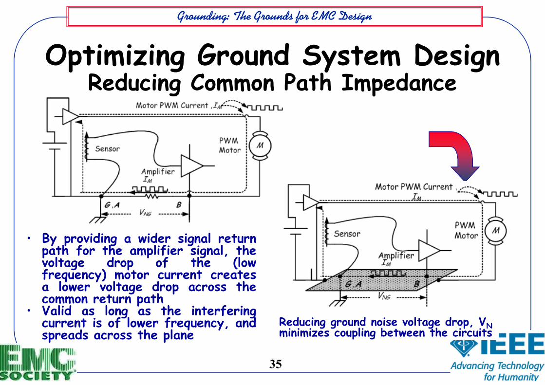
Reducing ground noise voltage drop, VNminimizes coupling between the circuits
Optimizing Ground System DesignReducing Common Path Impedance
• By providing a wider signal returnpath for the amplifier signal, thevoltage drop of the (lowfrequency) motor current createsa lower voltage drop across thecommon return path
• Valid as long as the interferingcurrent is of lower frequency, andspreads across the plane

Grounding: The Grounds for EMC Design
36
Avoiding IM Circulation through Signal Return Path Impedance
Sensor
IM
M
IM
BA
Optimizing Ground System DesignAvoiding A Common Impedance Path
Sensor
IM
M
IM
A,B
• By providing a dedicated signalreturn path for the amplifiersignal, all the way to the amplifiercommon (point B), the motorcurrent does not flow through thecommon impedance, and nointeraction occurs
• Valid as long as the sensor itselfis not grounded!

Grounding: The Grounds for EMC Design
37
Optimizing Ground System DesignGoals of Equipment and System Level
Grounding System• The grounding scheme inside a system must accomplish the
following goals: Analog, low level circuits must have extremely noiseless
dedicated returns; typically wires are used, dictating a single point, “star” grounding scheme
Analog, high frequency circuits (RF, video, etc.) must have low impedance, noise free return circuits, generally in form of planes or their extensions (e.g., coaxial cables)
Digital, logic circuit returns, especially high speed digital circuit returns, must have low impedance over the entire bandwidth (determined by the “edge rates” ), as power and signal returns share the same paths
Returns of powerful loads (e.g., solenoids, motors, relays, lamps, etc.) should be separated from all the above, even if they end up at the same power supply output terminal

Grounding: The Grounds for EMC Design
38
Ground System Topologies• Ground system topology is determined by several factors:
Signal Characteristics
System dimensions
System-specific separation & isolation requirements
Safety requirements
• The main ground system topologies are: A “floating” system
Single-point ground
Multi-point ground
POWER
ANALOG
AUDIO
DIGITAL
PWM
SYSTEM GROUNDING
It isNO MAGIC!!!

Grounding: The Grounds for EMC Design
39
Ground System Topologies A “Floating” System
Grounding: The Grounds for EMC Design
40
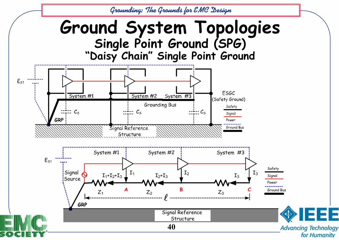
Ground System Topologies Single Point Ground (SPG)
“Daisy Chain” Single Point Ground
SSignal Reference
Structure
Safety
Signal
Power
Ground BusZ3Z2Z1
I1 I2 I3I2+I3I1+I2+I3 I3
A B C
GRP
Signal Source
ES1
llll
System #1 System #2 System #3

Grounding: The Grounds for EMC Design
41
Ground System Topologies Single Point Ground (SPG)Single Point (“Star”) Ground
S
ES1
Signal Reference
Structure
Safety
Signal
Power
VNG
ZGIN
Z3Z2Z1
I3I2
I1
Signal Source
GRPllll
System #1 System #2 System #3

Grounding: The Grounds for EMC Design
42
• At higher frequencies, where the length of the groundconductors approaches λλλλ/4, the SPG is ineffective
Distance along GND Conductor
λ/4
ZS
0
This circuit should ideally be grounded every λλλλ/10÷ λλλλ/20!
Ground System Topologies Single Point Ground (SPG)
A standing wave (black) depicted as the sum of two propagating waves traveling in opposite directions
(red and blue).
inZ →∞

Grounding: The Grounds for EMC Design
43
Ground System Topologies Multi-Point Ground (MPG)

Grounding: The Grounds for EMC Design
44
• But… It is not a cure for all• Unlike the Holy Grail,,,
• Careful design is still required
Ground System Topologies Multi-Point Ground (MPG)

Grounding: The Grounds for EMC Design
45
• When a system comprises of several types of circuits,a composite grounding topology may be used
Single point grounding, for low frequencies (d ≤ λ/20 MHz)
Multi-point grounding for high frequencies (d > λ/20 MHz)
Ground System Topologies Hybrid Grounding

Grounding: The Grounds for EMC Design
46
Equipment-Level “Ground Tree” Design Process
• Identify circuits• Define Chassis Ground connections at the circuit level (heat-sink
and RF Ground)• Define PCB-level signal returns (ground) requirements• Identify isolation requirements• Define local ground connections• Define CGP/SPG location• Connect GNDs from circuits and Power Supply to CGP• Identify “special cases” (GND System Violations) and potential
ground loops• Incorporate “isolation measures” (transformers, optocouplers,
balanced interfaces, e.g.RS-422 and Isolated Ground Connections)• Define special power supply outputs and connect returns to the
CGP when applicable; define special isolated outputs

Grounding: The Grounds for EMC Design
47
/
.
/
5
15
5/3.3
15
5
5
5 /
15 /
15 /
28 /
DC/DC Module
5
3.3
15
5
5 /
15 /
5 /
15 /
15 /
28 /
Equipment-Level “Ground Tree” Design Process
CGP
V VDVA
VA RF
VD RF
VA RF
VA RF
VD
LOOP ???
.
/
VA
VD/
Enclosure Chassis
VA
VD

Grounding: The Grounds for EMC Design
48
• No Isolation: PossibleSystem-Wide GroundLoops
• Isolated Power Supplies:Ground Loops throughPrimary Circuit Eliminated
Role of Switch-Mode Power Supplies in Grounding System Design

Grounding: The Grounds for EMC Design
49
Understanding and Precluding“Ground Loops”
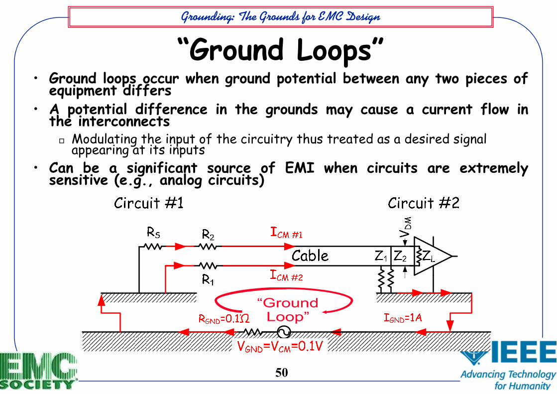
Grounding: The Grounds for EMC Design
50
“Ground Loops”• Ground loops occur when ground potential between any two pieces of
equipment differs• A potential difference in the grounds may cause a current flow in
the interconnects Modulating the input of the circuitry thus treated as a desired signal
appearing at its inputs
• Can be a significant source of EMI when circuits are extremelysensitive (e.g., analog circuits)
“Ground Loop”

Grounding: The Grounds for EMC Design
51
A model for illustrating the effect of grounding topology on system performance
CA
d= ⋅ε ε π
0
91 36 10= × F m/
C=Capacitance of PCB to Ground
“Ground Loops”
Circuit #1 Circuit #2
ICM#1
ICM#2
VSRS
=VCM
Transmission Line
VL
C d
A
C
A
d
VS
ZS
Z2
Z1
ZCM
R1
R2
ZL
h
S

Grounding: The Grounds for EMC Design
52
“Ground Loops”
Longitudinal Conversion Loss factor, LCL:
Constant
20'
CMdB
DMVo
VLCL Log
V=
= ⋅

Grounding: The Grounds for EMC Design
53
“Ground Loops”
• At Low Frequencies Capacitances, C, are dominant
Circuit impedance reduces with Frequency (f)
CM current increases with f
DM voltage increases with f
• At High Frequencies Low Pass Characteristics of the
transmission line are dominant Circuit impedance increases with f Termination impedance limits line
currents
Both sides floated
Floated Both Ends
Frequency [Hz]
Lo
ad
DM
Vo
lta
ge

Grounding: The Grounds for EMC Design
54
“Ground Loops”
• At Low Frequencies Circuit series impedance, due
to the capacitances, C, is reduced
CM current (and DM voltage) increases
• At High Frequencies No change from previous case
One side grounded
Floated One End
Frequency [Hz]
Lo
ad
DM
Vo
lta
ge

Grounding: The Grounds for EMC Design
55
“Ground Loops”
• At Low Frequencies Circuit series impedance, is
independent of capacitances, C
Circuit impedance determined by wiring & Load resistance (R)
CM current (and DM voltage) independent of f
• At High Frequencies No change from previous
cases
Both sides grounded
Grounded Both Ends
Frequency [Hz]
Lo
ad
DM
Vo
lta
ge

Grounding: The Grounds for EMC Design
56
Ground System Topologies
• Low frequency circuits Single point grounding only Floating provides marginal improvement and increased risk Low frequency performance is strongly dependent on the circuit grounding
topology Low frequency performance significantly degraded with multipoint grounding
• High frequency circuits Multipoint grounding only High frequency performance independent of grounding topology

Grounding: The Grounds for EMC Design
57
“Ground Loops” Techniques for Opening “Ground Loops”
Isolation Transformer
• Signal is coupled magnetically, thus the transformer inserts a high longitudinalimpedance in series with the CM current path
• Common Mode decoupling of 100-140 dB can be achieved @ f=1kHz• Expensive, frequency limited, and not always practical for signal circuits

Grounding: The Grounds for EMC Design
58
“Ground Loops” Techniques for Opening “Ground Loops”
BALUNs (Common Mode Chokes)
CM
Current
Signal DM
Current
Core
Hi µ−
CM-Generated
Flux
DM-Generated
Flux
• Inserts high-Z for CM signals, while passed “unnoticed” byDM currents - A “mode-selective filter”
• CM rejection > 80-100 dB can be achieved @ high-f’s• Bulky; can be implemented by Ferrite beads

Grounding: The Grounds for EMC Design
59
“Ground Loops” Techniques for Opening “Ground Loops”
Optical Isolator/Optocoupler
• Signal is coupled optically, thus the opto-isolator inserts a high longitudinal impedance in series with the CM current path
• Common Mode decoupling of 60-80 dB can be achieved• Mainly for digital circuits

Grounding: The Grounds for EMC Design
60
“Ground Loops” Techniques for Opening “Ground Loops”
Isolation Amplifier
• Grounds isolation within the two stages of the buffer amplifier• Each stage referenced to its associated ground• Common Mode decoupling of 60-80 dB (*) can be achieved
(*) 120 dB in special applications

Grounding: The Grounds for EMC Design
61
“Ground Loops” Techniques for Opening “Ground Loops”
Circuit Bypassing
• Basically a HF filtering mechanism, shunting CM noise to ground• Care to be paid not to “kill” the intended signal• Performance depends on value of capacitors, often requiring
combination of several approaches

Grounding: The Grounds for EMC Design
62
“Ground Loops” Techniques for Opening “Ground Loops”
Example: 10/100BaseT Interface
Typical 10/100BaseT Receive andTransmit Interfaces CircuitConsists of Balancing Magnetics andBypass Capacitors
TransmitInterface
Receive Interface

Grounding: The Grounds for EMC Design
63
Just tell me what rules I need to follow to ensure that I don’t have
EMC-related problems with my Grounding design.
Just tell me what rules I need to follow to ensure that I don’t have health-related problems with my
brain surgery.Courtesy: Prof. T. Hubing
Clemson University
Summary: Grounding Design RulesWhat are the most important Grounding & Shielding design
guidelines?

Grounding: The Grounds for EMC Design
64
for your Attention!!!

Grounding: The Grounds for EMC Design
65
Questions?
Comments?
Snide Remarks?
Grounding: The Grounds for EMC Design
66
For Further information:
Elya B. Joffe