growing crystals with your eyes open
TRANSCRIPT
Company ProfiZe
Growing crystals with your eyes open
Tom Ryan, Philips Material Characterization Systems
Philips Material Characterization Systems has been a leading supplier of characterization tools to the compound semiconductor industry for over a decade. As the industry shifts from high-end military and telecomms customers towards the low unit price/high volume world of consumer products, the need for powerful characterization tools becomes more and more pressing.
C haracterization is a key enabler in the development of semi- conductor technology and in
improving semiconductor manufac- turing.
This is especially true in the field of compound semiconductors, where inherently complicated materials are being used in increasingly compli- cated structures - while commercial pressures force prices steadily down- wards.
The pressure is on to increase yields, reduce cycle times and elimi- nate waste.
Better yields through better measurements The drive for higher yields coincides with a demand for even tighter speci- fication windows. It is now common to specify the thickness and indium composition of channel layers in HEMTs to a fraction of a per cent over 4-in epiwafers while the s,pecfication window for Fabry-Perot cavities in VCSELs is often a fraction of a nan- ometer.
At the other end of the scale, high volume products like LEDs may be less demanding in terms of specifica- tions, but the economic pressures to maximize yields are even more intense.
These forces have created a need for non destructive, wholewafer char- acterization techniques. Production wafers can be examined at an early
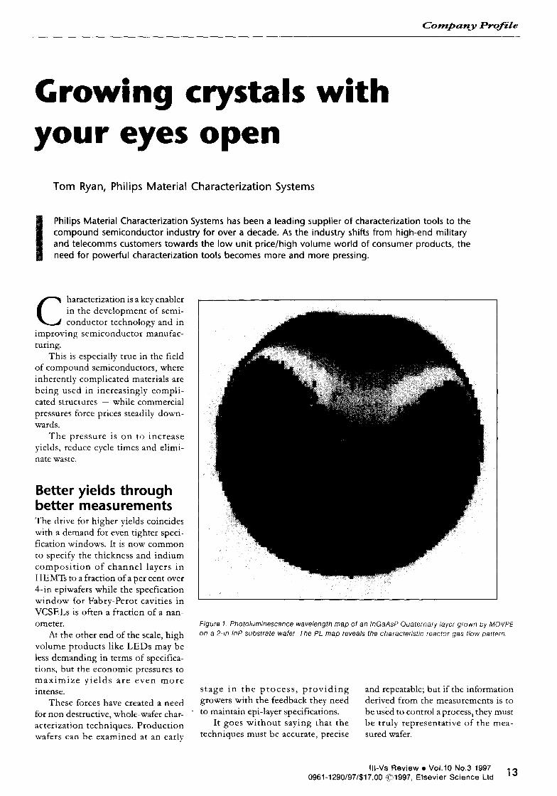
figure 1. Photoluminescence wavelength map of an /nGaAsP Quaternary layer grown by MOVPE
on a 2-in InP substrate wafer. The PL map reveals the characterfstfc reactor gas flow pattern
stage in the process, providing and repeatable; but if the information growers with the feedback they need derived from the measurements is to to maintain epi-layer specifications. be used to control a process7 they must
It goes without saying that the be truly representative of the mea- techniques must be accurate, precise sured wafer.
Ill-Vs Review ??Vol.10 No.3 1997 0961-1290/97/$17.00 01997, Elsevier Science Ltd
, 3
BetterYields Througl i
RESlSTMlY X-RAY DIFFRACTION
Artist’s lnterpreration
MFFRACTlON LUMINESCENCE A
Post-Epitaxial Processing -__
Company ProfiZe
The need for accurate statistics Materials properties can, and do, vary across a typical epi-wafer.Variations in substrate quality, reactor geometry and edge effects all have an influence on the measurement.
One measurement point at the cen- tre of a wafer does not give any infor- mation on uniformity. A nine point grid may give a more accurate estimate of the average properties of a wafer - but many more points are required to make a reliable estimate of the variabil- ity.
In fact, for a statistically significant measurement at least 150 points are needed, meaning the measurement technique has to be fast and highly automated.
Substrate screening If specifications are to be met, and yields optimized, screening of wafers has to start right at the beginning of the process - with the substrate.
The defining properties of a sub- strate wafer are crystal quality and doping. X-ray diffraction (XRD) rock- ing curve mapping is a powerful tech- nique for quantitative evaluation of substrates.
A combination of peak width, in- tensity and position information can be used to detect dislocation densities, polishing defects, low angle grain boundaries and lattice warp. Similarly, doping patterns in semi-insulating substrates can be obtained by resistiv- ity mapping.
Once correlations between a sub- strate parameter and device perfor- mance have been established, wafers with a low potential yield can be re- jected before any money is invested in them.
Reactor optimization The role of whole wafer mapping in setting up and optimizing an epitaxial growth reactor was summed up by the user of a photoluminescence (PL) mapping system. “Before we bought the PL mapper, we were growing crys-
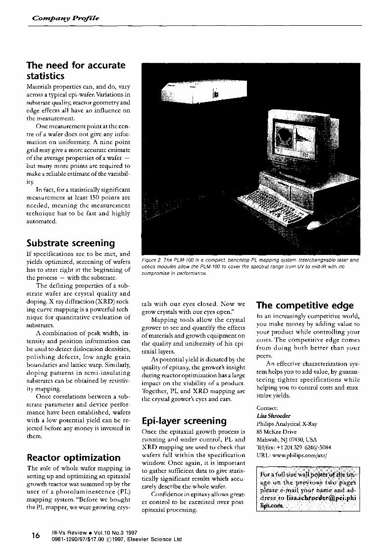
Figure 2. The PLM-100 is stem. interchangeable laser and opt/es modules allow the PLM-700 to cover the spectral range from UV to mid-/R with no compromise in performance
tals with our eyes closed. Now we grow crystals with our eyes open.”
Mapping tools allow the crystal grower to see and quantify the effects of materials and growth equipment on the quality and uniformity of his epi- taxial layers.
As potential yield is dictated by the quality of epitaxy, the grower’s insight during reactor optimization has a large impact on the viability of a product. Together, PL and XRD mapping are the crystal grower’s eyes and ears.
Epi-layer screening Once the epitaxial growth process is running and under control, PL and XRD mapping are used to check that wafers fall within the specification window. Once again, it is important to gather sufficient data to give statis- tically significant results which accu- rately describe the whole wafer.
Confidence in epitaxy allows great- er control to be exercised over post- epitaxial processing.
The competitive edge In an increasingly competitive world, you make money by adding value to your product while controlling your costs. The competitive edge comes from doing both better than your peers.
An effective characterization sys- tem helps you to add value, by guaran- teeing tighter specifications while helping you to control costs and max- imize yields.
Contact: Lisa Shroeder Philips Analytical X-Ray 85 McKee Drive Mahwah, NJ 07430, USA Tel/fax: +1201529-6246/-5084 URL: www.philips.com/axr/
16 Ill-Vs Review ??Vol.10 No.3 1997 0961-1290/97/$17.00 01997, Elsevier Science Ltd