growth and photoconductor properties of hgcdte epilayers grown by hot wall epitaxy method
TRANSCRIPT

Journal of Crystal Growth 240 (2002) 135–141
Growth and photoconductor properties of HgCdTe epilayersgrown by hot wall epitaxy method
K.J. Honga,*, J.W. Jeonga, H.W. Baeka, T.S. Jeongb, C.J. Younb,J.D. Moonc, J.S. Parkd
aDepartment of Physics, Chosun University, Kwangju 501-759, South KoreabDepartment of Physics and Semiconductor Physics Research Center (SPRC), Jeonbuk National University,
Jeonbuk 560-756, South KoreacDepartment of Photoelectronics, Dongshin University, Naju 520-714, South Korea
dDivision of Metallurgical and Material Science Engineering, Chosun University, Kwangju 501-759, South Korea
Received 20 August 2001; accepted 13 November 2001
Communicated by M. Schieber
Abstract
Hg1�xCdxTe (MCT) was grown by hot wall epitaxy. Prior to the MCT growth, the CdTe (1 1 1) buffer layer was
grown on the GaAs substrate at the temperature of 5901C for 15min. When the thickness of the CdTe buffer layer was
5mm or even thicker, the full-width at half-maximum values obtained from the X-ray rocking curves were found to
significantly decrease. After a good quality CdTe buffer layer was grown, the MCT epilayers were grown on the
CdTe(1 1 1) /GaAs substrate at various temperatures in situ. The crystal quality for those epilayers was investigated by
means of the X-ray rocking curves and the photocurrent experiment. The photoconductor characterization for the
epilayers was also measured. The energy band gap of MCT was determined from the photocurrent measurement and
the x composition rates from the temperature dependence of the energy band gap were also obtained.r 2002 Elsevier
Science B.V. All rights reserved.
PACS: 78.20.�e; 81.15.Hi; 85.60.Gz
Keywords: A3. Hot wall epitaxy
1. Introduction
Hg1�xCdxTe (MCT) is an important electro-optical band gap semiconductor for infraredregion (IR) detector technology due to the ease
of wavelength tunability [1]. However, the detec-tion of wavelength is very sensitive to the alloycomposition, x: Currently, IR sensor and imagingarray development has focused on the detection ofa single band of IR radiation typically in one ofthe following three atmospheric transmissionwindows such as 1–2.5, 3–5, and 8–12 mm. How-ever, although the MCT epilayers on a bulk CdTecould be grown by various epitaxial methods, the
*Corresponding author. Tel.: +82-62-230-6637; fax: +82-
62-234-4326.
E-mail address: [email protected] (K.J. Hong).
0022-0248/01/$ - see front matter r 2002 Elsevier Science B.V. All rights reserved.
PII: S 0 0 2 2 - 0 2 4 8 ( 0 1 ) 0 2 0 9 2 - 9

current lack of availability of high-quality andlarge-area CdTe substrates is generally recognizedas a main limitation for efficient MCT detectortechnology. Recently, epitaxial MCT layers havebeen grown on lattice-matched CdZnTe substratesby liquid phase epitaxy (LPE), metalorganicchemical vapor deposition (MOCVD), and mole-cular beam epitaxy (MBE) techniques [2–5]. Thus,MOCVD and MBE have recently improved theCdTe epitaxial films. These CdTe films wereepitaxially grown on foreign substrates like sap-phire, GaAs, and Si [6–9]. These substrates areavailable at low cost, in large area, with goodstructural quality and CdTe is an ideal buffermaterial for the subsequent growth of epitaxialMCT. Moreover, GaAs and Si are the basicmaterials for the fabrication of electronic circuits,so that the IR detector and the signal processingcircuit on a single chip could be integrated on theMCT layer deposited on such a substrate. How-ever, until now the cost of device-quality MCT/Siand MCT/GaAs substrates, grown by MOCVDand MBE, is too high for commercial applications.Compared with these methods, the hot wallepitaxy (HWE) technique has the advantages oflow cost, simplicity, convenience and relativelylarge growth rate under the thermodynamicequilibrium growth.In this paper, MCT on the CdTe buffer layer
was grown by using a HWE method. Here, theCdTe buffer layers were grown under variousgrowth conditions on the semi-insulating GaAs(1 0 0). The crystal quality of the grown MCTs wasestimated by means of the powder and the doublecrystal X-ray diffraction technique. Also, thephotoconductor characterization for these epi-layers is examined through a photocurrent (PC)measurement.
2. Experimental procedure
A homemade HWE apparatus was used forgrowing the MCT epilayers on the GaAs sub-strates. This HWE apparatus consist of the twoelectric furnaces, made of a quartz tube withkanthal wire. And a substrate holder is placed onthe top of the furnace and is easily switched on the
top of the two furnaces as shown in Fig. 1. Here,the first furnace shown in Fig. 1(a) is necessary togrow the CdTe buffer layer without influencing theHgTe powder. If the second furnace shown inFig. 1(b) is used to grow the CdTe buffer layer,then HgTe powder in the furnace located belowthe CdTe furnace is simultaneously evaporatedduring the CdTe buffer growth because theevaporation temperature of the HgTe powder isvery low. Therefore, HWE apparatus was used forthe separated furnaces for the CdTe buffer growthof Fig. 1(a) and the MCT growth of Fig. 1(b).Prior to growth, the semi-insulating GaAs (1 0 0)
substrate was cleaned ultrasonically for 1min insuccessive baths of trichloroethylene, acetone,methanol, and 2-propanol and etched for 1 minin a solution of H2SO4:H2O2:H2O (5:1:1). The
Fig. 1. Schematic diagram of a HWE apparatus on the growth
furnaces: (a) The first furnace shown in Fig. 1(a) was used to
grow the CdTe buffer layer without influencing the HgTe
power. (b) After the CdTe buffer layer growth, the second
furnace shown in Fig. 1 (b) was used to grow the MCT epilayer
on the CdTe buffer layer.
K.J. Hong et al. / Journal of Crystal Growth 240 (2002) 135–141136

substrate was degreased in organic solvents, andrinsed with deionized water (18.2MO). After thesubstrate was dried off, the substrate was im-mediately loaded onto the substrate holder in theHWE. The GaAs substrate was annealed in apreheating process to remove the oxide of thesubstrate surface. Fourie et al. [10] reported thatthe grown CdTe showed (1 0 0) and (1 1 1) planesdepending on the preheating temperature. In thisexperiment, after the GaAs substrates were an-nealed at the temperature of 5501C and above orbelow as a preheating process, the CdTe bufferlayers on the preheated substrates were grown byusing the (a) furnace as shown in Fig. 1. The CdTebuffer layers were grown while the temperature ofthe substrate was set at 2801C and the sourcetemperature, source 1, was set at 4601C, respec-tively. The grown CdTe buffer layers with athickness of 3 mm were examined by using theX-ray diffraction powder method. From theseresults, we confirmed that the samples preheatedbelow 5501C were (1 0 0) plane and the samplespreheated above 5501C were the (1 1 1) plane,
respectively, as shown in Fig. 2. Also, the full-width at half-maximum (FWHM) values of thesesamples were measured by using the double crystalrocking curve (DCRC) experiment. The preheatedsample for 15min at 5901C showed a minimumFWHM value. And the grown CdTe on thesesubstrates was revealed to be the (1 1 1) plane. TheHgCdTe/CdTe/GaAs epilayers were grown withHWE, while the substrate was switched succes-sively on top of the (a) and (b) furnace as shown inFig. 1. The source materials 1 and 2 as shown inFig. 1 were CdTe and HgTe powder (RareMetallic, 6N), respectively. After the CdTe bufferepilayer on the GaAs was grown in the (a) furnace,the CdTe/GaAs epilayer was immediately movedto the (b) furnace. Then, the HgCdTe/CdTe/GaAsepilayer was grown by using the heating sources 1and 2, simultaneously. The grown epilayers wereanalyzed by DCRC to obtain the optimum growthcondition. The thickness of the grown samples wasmeasured by an a-step profilometer (Tencor, a-step 200). Also, in order to measure the PCspectra, the electrodes were made on both the endsof the sample and connected to a gold wire. Theelectrode space was 100 mm. After this, the samplewas mounted on the holder in the low temperaturecryostat equipment, the PC spectrum measure-ment was made while the monochromatic lightemitted from light source that passed through achopper was illustrated on the sample. Thisexperiment was carried out at the temperature of77K by using the light emitted from a halogenlamp and a 6001C black body radiation.
3. Results and discussion
3.1. Growth of the MCT epilayers
In general, the quality of the MCT epilayers hasbeen known to be strongly dependent on that ofthe CdTe buffer layer. The quality of CdTeepilayer was influenced by both the Ga outdiffusedfrom the GaAs substrate and the defects generatedat the interface due to the misfit layers. To reducethe Ga outdiffusion and the defect generation, theproper thickness of the CdTe buffer layer must bechosen to grow a high-quality MCT epilayers on
Fig. 2. The growth orientation of the CdTe epilayers deter-
mined by the preheating condition of the substrate.
K.J. Hong et al. / Journal of Crystal Growth 240 (2002) 135–141 137

the CdTe/GaAs substrate. Therefore, the CdTebuffer layers in the thickness ranging between 0.8and 12 mm were grown at 2801C to find theoptimum buffer layer, prior to the MCT growth.Fig. 3 shows FWHM values as a function of the
thickness of the CdTe epilayers grown on theGaAs (1 0 0) substrates. The FWHM valuesremarkably decreased when the thickness of theCdTe layer was 5 mm or even thicker. These resultsindicate that the biaxial compressive stress of theCdTe epilayers on GaAs is significantly relaxedwith increasing CdTe thickness. As is listed inTable 1, the optimum growth temperatures of thesubstrate and source 1 for the CdTe (1 1 1)epilayers were found to be 2801C and 4601C,respectively. At that time, the thickness of theCdTe (1 1 1) epilayer was 9 mm and the minimumFWHM value was 139 arcsec, respectively. Thisthickness was comparable to the reported thick-ness, 10 mm, of high-quality CdTe grown by HWE[11]. Then, the MCT epilayers were grown in situon the CdTe(1 1 1)/GaAs(1 0 0) substrate with theapparatus as shown in Fig. 1(a) and (b). As is
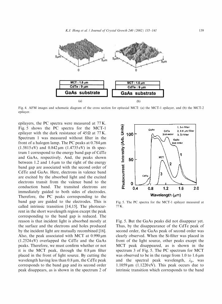
listed in Table 1, the heating temperatures ofsources 1 and 2 for the MCT-1 sample were set at3801C and 1851C, respectively. Also, the heatingtemperatures of sources 1 and 2 for the MCT-2sample were maintained at 3601C and 1901C,respectively. The substrate temperature was main-tained at 1701C, while the MCT samples weregrowing. The growth rates of the MCT-1 and 2samples were 0.9 and 0.8 mm/h, respectively. Also,the FWHM values obtained from DCRC analysisfor the MCT-1 and 2 samples were determined tobe 125 and 120 arcsec, respectively. These valuesare comparable with other MCT samples grownby MBE [12] and MOCVD [13]. It should be notedthat the crystalline quality of the MCT epilayers isbetter than that of the CdTe/GaAs substrateepilayers. The surface morphologies observed byatomic force microscopy (AFM) and the schematiccross section of the epitaxial grown MCT sampleswere shown in Fig. 4. The root-mean-squarevalues, Rms; for the surface roughness of theMCT-1 and 2 samples were obtained to be 7 and9 nm, respectively.
3.2. Photocurrent measurement
Single crystal semiconductors have two types ofphotoconduction, extrinsic and intrinsic. In theextrinsic case, a free electron in an n-typephotoconductor, or a free hole in a p-typephotoconductor is created through the impuritylevels when the light illuminates the semiconduc-tor. However, intrinsic photoconductor like MCTdepends upon the band-to-band transition and afree electron and hole generated simultaneously bythe illuminated light. Also, the cut-off wavelengthis determined by the band gap energy of theintrinsic photoconductor. Therefore, to character-ize the photoconductor for the grown MCT
Fig. 3. The dependence of FWHM of the XRD rocking curves
on the thickness of the CdTe epilayers.
Table 1
Optimum growth conditions for the MCT epilayers
CdTe (1C) MCT-1 MCT-2
Substrate Tem. 280 1701C 1701C
Source 1 Tem. 460 3801C 3601C
Source 2 Tem. 1851C 1901C
Composition x 0.762 0.317
K.J. Hong et al. / Journal of Crystal Growth 240 (2002) 135–141138
epilayers, the PC spectra were measured at 77K.Fig. 5 shows the PC spectra for the MCT-1epilayer with the dark resistance of 45O at 77K.Spectrum 1 was measured without filter in thefront of a halogen lamp. The PC peaks at 0.784 mm(1.5815 eV) and 0.842 mm (1.4735 eV) in th spec-trum 1 correspond to the energy band gap of CdTeand GaAs, respectively. And, the peaks shownbetween 1.2 and 1.6 mm to the right of the energyband gap are associated with the second order ofCdTe and GaAs. Here, electrons in valence bandare excited by the absorbed light and the excitedelectrons transit from the valence band to theconduction band. The transited electrons areimmediately guided to both sides of electrodes.Therefore, the PC peaks corresponding to theband gap are guided to the electrodes. This iscalled intrinsic transition [14,15]. The photocur-rent in the short wavelength region except the peakcorresponding to the band gap is reduced. Thereason is that incident light is absorbed mostly atthe surface and the electrons and holes producedby the incident light are mutually recombined [16].Also, the peak associated with MCT at 0.990 mm(1.2524 eV) overlapped the CdTe and the GaAspeaks. Therefore, we must confirm whether or notit is the MCT peak, through the 0.8 mm filterplaced in the front of light source. By cutting thewavelength having less than 0.8 mm, the CdTe peakcorresponds to the band gap and its second orderpeak disappears, as is shown in the spectrum 2 of
Fig. 5. But the GaAs peaks did not disappear yet.Thus, by the disappearance of the CdTe peak ofsecond order, the GaAs peak of second order wasclearly observed. When the Si-filter was placed infront of the light source, other peaks except theMCT peak disappeared, as is shown in thespectrum 3 of Fig. 5. The PC spectrum for MCTwas observed to be in the range from 1.0 to 1.6 mmand the spectral peak wavelength, lp; was1.1059 mm (1.1220 eV). This peak occurs due tointrinsic transition which corresponds to the band
Fig. 5. The PC spectra for the MCT-1 epilayer measured at
77K.
Fig. 4. AFM images and schematic diagram of the cross section for epitaxial MCT: (a) the MCT-1 epilayer, and (b) the MCT-2
epilayer.
K.J. Hong et al. / Journal of Crystal Growth 240 (2002) 135–141 139

gap of the MCT epilayer. Therefore, Eq. [17] forthe composition and temperature dependence ofthe energy band gap of the MCT epilayer wasgiven as
Eg ¼ ½�304þ 0:63T2ð1� 2xÞ=ð11þ TÞ
þ 1858x þ 54x2�meV; ð1Þ
where Eg and T were the energy band gap and theabsolute temperature, respectively. This equationwas used to calculate the composition rate for thex value of Hg1�xCdxTe. From Eq. (1), the x valueof lp for MCT at 77K is estimated to be 0.762.And the cut-off wavelength, lc; is 1.2632 mm(0.9815 eV), which denotes the band width wave-length of the half intensity for maximum intensityof lp:Fig. 6 shows the PC spectrum of the MCT-2
epilayer measured at 77K using a 6001C blackbody source, while the dark resistance of thissample at the same temperature was measured as60O: As is shown in Fig. 6, the PC spectrum ofMCT appeared in the wavelength range from 3.5to 5.5 mm. Thus, lp; which corresponds to theintrinsic transition and lc were 4.0750 (0.3043 eV)and 4.5600 mm (0.2719 eV), respectively. FromEq. (1), the x value of lp for the MCT-2 epilayerat 77K turned out to be 0.317. Also, thecomparatively steep slope to the long wavelength
region of the spectra shown in Figs. 5 and 6 wasthought to be an evidence of homogeneity of thecomposition in the surface epilayer.
4. Conclusions
Hg1�xCdxTe was grown by hot wall epitaxymethod. The (1 1 1) CdTe buffer epilayer wasgrown on the GaAs substrate at 5901C for 15min.Then, MCT epilayers were grown on the grownCdTe buffer epilayer. The grown MCT epilayerswere confirmed to be of high-quality crystal andthe extremely smooth surface was proven by usingDCRC and AFM measurement. From the PCmeasurement, MCT-1 showed the spectrum rangefrom 1.0 to 1.6 mm, and the spectral peakwavelength located at 1.1059 mm (1.1220 eV) cor-responds to the band gap of the MCT epilayer.The spectrum of MCT-2 was observed within thewavelength range from 3.5 to 5.5 mm and itsspectral peak was located at 4.0750 mm(0.3043 eV). The x values of composition rate forthe MCT-1 and 2 epilayers at 77K turned out tobe 0.762 and 0.317, respectively. Also, the com-paratively steep slopes on the region to the right ofthe spectral peaks wavelength as shown in Figs. 5and 6 were thought to be an evidence of thehomogeneity of the composition in the surfaceepilayers. Therefore, these results mean that thegrown MCT epilayers can be applied as aphotoconductor for the infrared region detector.
Acknowledgements
This study was supported in part by researchgrants from chosun university, 2000.
References
[1] R. Korenstein, P. Hallock, B. MacLeod, J. Vac. Sci.
Technol. B 9 (1991) 630.
[2] B. Pelliciari, J. Crystal Growth 86 (1988) 146.
[3] I. Bath, J. Crystal Growth 117 (1992) 1.
[4] J.M. Arias, S.H. Shin, J.G. Pasko, R.E. DeWames, E.R.
Gertner, J. Appl. Phys. 65 (1989) 1747.
Fig. 6. The PC spectrum for the MCT-2 epilayer measured at
77K.
K.J. Hong et al. / Journal of Crystal Growth 240 (2002) 135–141140

[5] P.S. Wijewarnasuriya, M. Boukerche, J.P. Faurie, J. Appl.
Phys. 67 (1990) 859.
[6] M. Kasuga, D. Kodama, H.H. Agiwara, K. Kagami, J.
Jpn. Assoc. Crystal Growth 21 (1994) 5377.
[7] K. Shigenaka, L. Sugiura, F. Nakata, K. Hirahara, J.
Crystal Growth 145 (1994) 145.
[8] S.H. Shin, J.M. Arias, D.D. Edwall, M. Zandian, J.G.
Pasko, R.E. DeWames, J. Vac. Sci. Technol. B 10 (1992)
1492.
[9] R. Sporken, Y.P. Chen, S. Sivananthan, M.D. Lange, J.P.
Faurie, J. Vac. Sci. Technol. B 10 (1992) 1405.
[10] J.P. Fourie, C. Hsu, S. Sivananthan, X. Chu, Surf. Sci. 168
(1986) 473.
[11] J.F. Wang, K. Kikuchi, B.H. Koo, Y. Ishikawa, W.
Uchida, M. Isshiki, J. Crystal Growth 187 (1998) 373.
[12] S.D. Chen, L. Lin, X. Z. He, M.J. Ying, R.Q. Wu, J.
Crystal Growth 152 (1995) 261.
[13] D.D. Edwall, J. Bajai, E.R. Gertner, J. Vac. Sci. Technol.
A 8 (1990) 1045.
[14] C.C. Klick, Phys. Rev. 89 (1953) 274.
[15] R.H. Bube, Phys. Rev. 101 (1956) 1668.
[16] R.H. Bube, Photoconductivity of Solids, Wiley, New
York, 1969, p. 391.
[17] M.H. Weiler, in: R.K. Willardson, A.C. Beer (Eds.),
Semiconductors and Semimetals, Vol. 16, Academic, New
York, 1981, p. 180.
K.J. Hong et al. / Journal of Crystal Growth 240 (2002) 135–141 141