gsm based distance calculation for transmission line fault
DESCRIPTION
GSM BASED DISTANCE CALCULATION FOR TRANSMISSION LINE FAULTTRANSCRIPT
INTRODUCTION
1.1 EMBEDDED SYSTEMS:
An embedded system is a special-purpose system in which the computer is
completely encapsulated by or dedicated to the device or system it controls.
Unlike a general-purpose computer, such as a personal computer, an embedded
system performs one or a few predefined tasks, usually with very specific
requirements. Since the system is dedicated to specific tasks, design engineers can
optimize it, reducing the size and cost of the product. Embedded systems are often
mass-produced, benefiting from economies of scale.
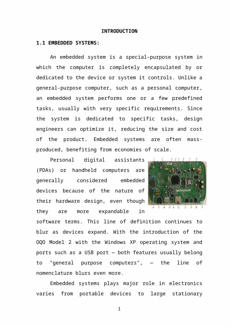
Personal digital assistants (PDAs) or handheld
computers are generally considered embedded
devices because of the nature of their hardware
design, even though they are more expandable in
software terms. This line of definition continues to
blur as devices expand. With the introduction of the
OQO Model 2 with the Windows XP operating
system and ports such as a USB port — both features usually belong to "general
purpose computers", — the line of nomenclature blurs even more.
Embedded systems plays major role in electronics varies from portable
devices to large stationary installations like digital watches and MP3 players,
traffic lights, factory controllers, or the systems controlling nuclear power plants.
In terms of complexity embedded systems can range from very simple with
a single microcontroller chip, to very complex with multiple units, peripherals and
networks mounted inside a large chassis or enclosure.
Examples of Embedded Systems:
Avionics, such as inertial guidance systems, flight control
hardware/software and other integrated systems in aircraft and missiles
Cellular telephones and telephone switches
Engine controllers and antilock brake controllers for automobiles
1

Home automation products, such as thermostats, air conditioners,
sprinklers, and security monitoring systems
Handheld calculators
Handheld computers
Household appliances, including microwave ovens, washing machines,
television sets, DVD players and recorders
Medical equipment
Personal digital assistant
Videogame consoles
Computer peripherals such as routers and printers.
Industrial controllers for remote machine operation.
1.2. INTRODUCTION TO THE PROJECT:
The project uses the standard concept of Ohms law i.e., when a low DC voltage is
applied at the feeder end through a series resistor (Cable lines), then current would vary
depending upon the location of fault in the cable. In case there is a short circuit (Line to
Ground), the voltage across series resistors changes accordingly, which is then fed to an
ADC to develop precise digital data which the programmed microcontroller of 8051
family would display in kilometers.
The project is assembled with a set of resistors representing cable length in KM’s
and fault creation is made by a set of switches at every known KM to cross check the
accuracy of the same. The fault occurring at a particular distance and the respective
phase is displayed on a LCD interfaced to the microcontroller.
GSM module is used to send a sms to the sub-station about phase fault and
distance calculated.
2

BLOCK DIAGRAM:
BLOCK DIAGRAM:
LCD display: Normal. Abnormal condition.
3 Phases should be there and each phase 4 switches. (Each switch 2KM)
GSM to send the msg regarding distance and fault phase
1.3. BLOCK DIAGRAM DESCRIPTION:
Power Supply: This section is meant for supplying Power to all the sections
mentioned above. It basically consists of a Transformer to step down the 230V ac
to 9V ac followed by diodes. Here diodes are used to rectify the ac to dc. After
rectification the obtained rippled dc is filtered using a capacitor Filter. A positive
voltage regulator is used to regulate the obtained dc voltage.
Microcontroller: This section forms the control unit of the whole project. This
section basically consists of a Microcontroller with its associated circuitry like
Crystal with capacitors, Reset circuitry, Pull up resistors (if needed) and so on.
3
MICRO CONTROLLER
8051
POWER
SUPPLY
VOLTAGE SENSING CIRCUIT
Relay
Fault switches
LCD(16x2)
GSM
R:NF Y:NF B:NF
Distance: 000KM
R:NF Y:F B:NF
Distance: 002KM
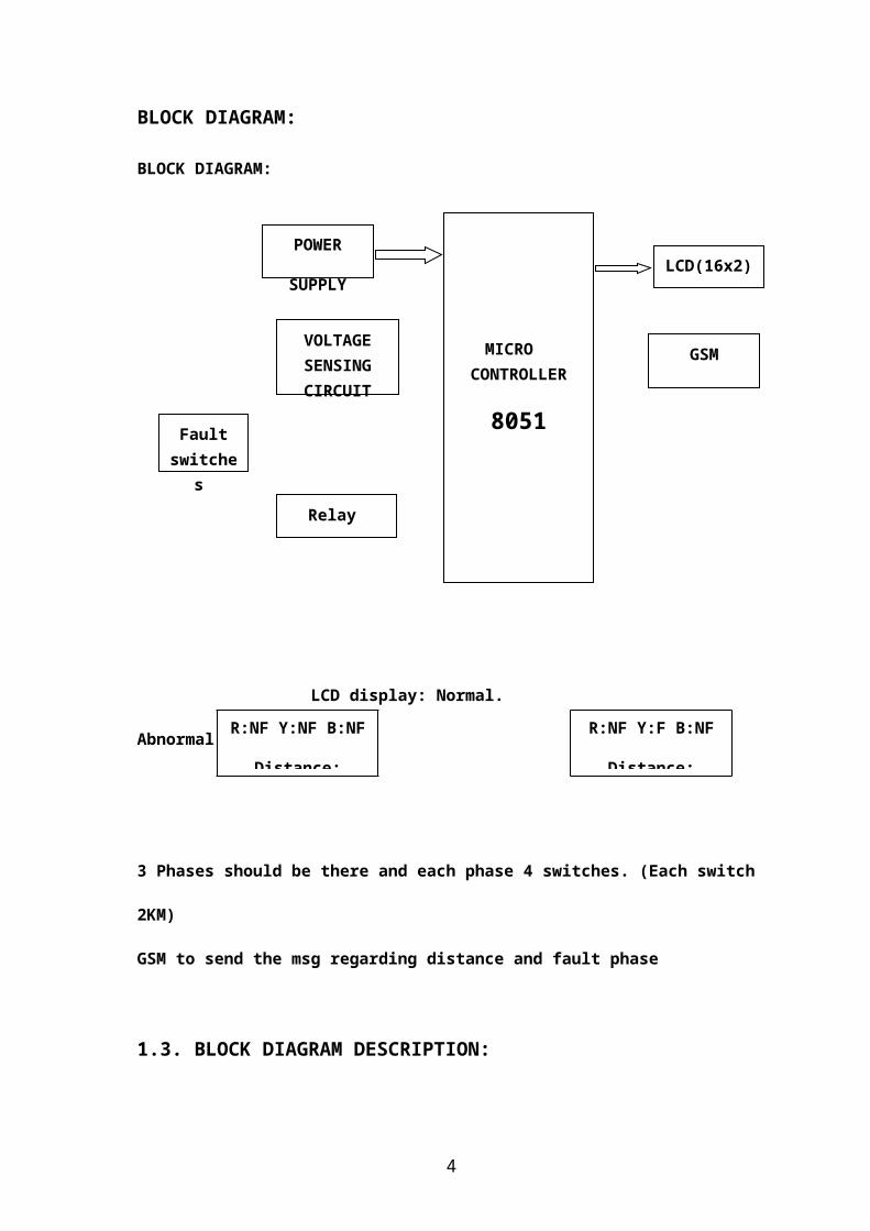
The Microcontroller forms the heart of the project because it controls the devices
being interfaced and communicates with the devices according to the program
being written.
LCD Display: This section is basically meant to show up the status of the project.
This project makes use of Liquid Crystal Display to display / prompt for
necessary information.
Relay Section: This section consists of an interfacing circuitry to switch ON /
OFF the system whenever any unhealthy conditions i.e. overload is detected. This
circuitry basically consists of a Relay, transistor and a protection diode. A relay is
used to drive the 230V devices.
SCHEMATIC:
4

SCHEMATIC DESCRIPTION:
Firstly, the required operating voltage for Microcontroller AT89S52 is 5V. Hence
the 5V D.C. power supply is needed by the same. This regulated 5V is generated by first
stepping down the 230V to 18V by the step down transformer.
In the both the Power supplies the step downed a.c. voltage is being rectified by
the Bridge Rectifier. The diodes used are 1N4007. The rectified a.c voltage is now
filtered using a ‘C’ filter. Now the rectified, filtered D.C. voltage is fed to the Voltage
Regulator. This voltage regulator allows us to have a Regulated Voltage. In Power
supply given to Microcontroller 5V is generated using 7805 and in other two power
supply 12V is generated using 7812. The rectified; filtered and regulated voltage is again
filtered for ripples using an electrolytic capacitor 100μF. Now the output from the first
section is fed to 40th pin of AT89S52 microcontroller to supply operating voltage and
from other power supply to circuitry.
The microcontroller AT89S52 with Pull up resistors at Port0 and crystal
oscillator of 11.0592 MHz crystal in conjunction with couple of capacitors of is placed
at 18th & 19th pins of AT89S52 to make it work (execute) properly.
CIRCUIT DESCRIPTION:
DESCRIPTION:
The project uses the standard concept of Ohms law i.e., when a low DC voltage is
applied at the feeder end through a series resistor (Cable lines), then current would vary
depending upon the location of fault in the cable. In case there is a short circuit (Line to
Ground), the voltage across series resistors changes accordingly, which is then fed to an
ADC to develop precise digital data which the programmed microcontroller of 8051
family would display in kilometers.
The project is assembled with a set of resistors representing cable length in KM’s
and fault creation is made by a set of switches at every known KM to cross check the
5

accuracy of the same. The fault occurring at a particular distance and the respective
phase is displayed on a LCD interfaced to the microcontroller.
GSM module is used to send a sms to the sub-station about phase fault and
distance calculated.
HARDWARE REQUIRED:
Microcontroller
LCD
Switches
Power supply
Voltage sensing circuit
Relay
GSM
SOFTWARE TOOLS:
1. Embedded C
2. Keil Uvision3
3. Uc-Flash or ISP
6
HARD WARE EXPLANATION:
MICRO CONTROLLER 89C51
Introduction
A Micro controller consists of a powerful CPU tightly coupled with
memory, various I/O interfaces such as serial port, parallel port timer or counter,
interrupt controller, data acquisition interfaces-Analog to Digital converter,
Digital to Analog converter, integrated on to a single silicon chip.
If a system is developed with a microprocessor, the designer has to go for
external memory such as RAM, ROM, EPROM and peripherals. But controller is
provided all these facilities on a single chip. Development of a Micro controller
reduces PCB size and cost of design.
One of the major differences between a Microprocessor and a Micro controller is
that a controller often deals with bits not bytes as in the real world application.
Intel has introduced a family of Micro controllers called the MCS-51.
The Major Features:
Compatible with MCS-51 products
4k Bytes of in-system Reprogrammable flash memory
Fully static operation: 0HZ to 24MHZ
Three level programmable clock
128 * 8 –bit timer/counters
Six interrupt sources
Programmable serial channel
Low power idle power-down modes
Why AT 89C51
7
The system requirements and control specifications clearly rule out the use
of 16, 32 or 64 bit micro controllers or microprocessors. Systems using these may
be earlier to implement due to large number of internal features. They are also
faster and more reliable but, 8-bit micro controller satisfactorily serves the above
application. Using an inexpensive 8-bit Microcontroller will doom the 32-bit
product failure in any competitive market place.
Coming to the question of why to use AT89C51 of all the 8-bit
microcontroller available in the market the main answer would be because it has 4
Kb on chip flash memory which is just sufficient for our application. The on-chip
Flash ROM allows the program memory to be reprogrammed in system or by
conventional non-volatile memory Programmer. Moreover ATMEL is the leader
in flash technology in today’s market place and hence using AT 89C51 is the
optimal solution.
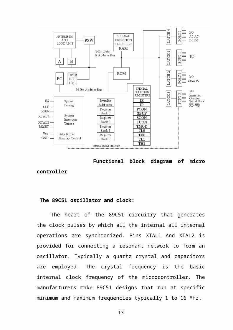
AT89C51 MICROCONTROLLER ARCHITECTURE
The 89C51 architecture consists of these specific features:
Eight –bit CPU with registers A (the accumulator) and B
Sixteen-bit program counter (PC) and data pointer (DPTR)
Eight- bit stack pointer (PSW)
Eight-bit stack pointer (Sp)
Internal ROM or EPROM (8751) of 0(8031) to 4K (89C51)
Internal RAM of 128 bytes:
1. Four register banks, each containing eight registers
2. Sixteen bytes, which maybe addressed at the bit level
3. Eighty bytes of general- purpose data memory
Thirty –two input/output pins arranged as four 8-bit ports:p0-p3
Two 16-bit timer/counters: T0 and T1
Full duplex serial data receiver/transmitter: SBUF
Control registers: TCON, TMOD, SCON, PCON, IP, and IE
Two external and three internal interrupts sources.
8
Oscillator and clock circuits.
Functional block diagram of micro controller
The 89C51 oscillator and clock:
The heart of the 89C51 circuitry that generates the clock pulses by which
all the internal all internal operations are synchronized. Pins XTAL1 And XTAL2
is provided for connecting a resonant network to form an oscillator. Typically a
quartz crystal and capacitors are employed. The crystal frequency is the basic
internal clock frequency of the microcontroller. The manufacturers make 89C51
designs that run at specific minimum and maximum frequencies typically 1 to 16
MHz.
9

Fig 3.7.2: - Oscillator and timing circuit
Types of memory:
The 89C51 have three general types of memory. They are on-chip memory,
external Code memory and external Ram. On-Chip memory refers to physically
existing memory on the micro controller itself. External code memory is the code
memory that resides off chip. This is often in the form of an external EPROM.
External RAM is the Ram that resides off chip. This often is in the form of
standard static RAM or flash RAM.
10

a) Code memory
Code memory is the memory that holds the actual 89C51 programs that is
to be run. This memory is limited to 64K. Code memory may be found on-chip or
off-chip. It is possible to have 4K of code memory on-chip and 60K off chip
memory simultaneously. If only off-chip memory is available then there can be
64K of off chip ROM. This is controlled by pin provided as EA
b) Internal RAM
The 89C51 have a bank of 128 of internal RAM. The internal RAM is
found on-chip. So it is the fastest Ram available. And also it is most flexible in
terms of reading and writing. Internal Ram is volatile, so when 89C51 is reset, this
memory is cleared. 128 bytes of internal memory are subdivided. The first 32
bytes are divided into 4 register banks. Each bank contains 8 registers. Internal
RAM also contains 128 bits, which are addressed from 20h to 2Fh. These bits are
bit addressed i.e. each individual bit of a byte can be addressed by the user. They
are numbered 00h to 7Fh. The user may make use of these variables with
commands such as SETB and CLR.
FLASH MEMORY:
Flash memory (sometimes called "flash RAM") is a type of constantly-
powered non volatile that can be erased and reprogrammed in units of memory
called blocks. It is a variation of electrically erasable programmable read-only
memory (EEPROM) which, unlike flash memory, is erased and rewritten at the
byte level, which is slower than flash memory updating. Flash memory is often
used to hold control code such as the basic input/output system (BIOS) in a
personal computer. When BIOS needs to be changed (rewritten), the flash
11
memory can be written to in block (rather than byte) sizes, making it easy to
update. On the other hand, flash memory is not useful as random access memory
(RAM) because RAM needs to be addressable at the byte (not the block) level.
Flash memory gets its name because the microchip is organized so that a
section of memory cells are erased in a single action or "flash." The erasure is
caused by Fowler-Nordheim tunneling in which electrons pierce through a thin
dielectric material to remove an electronic charge from a floating gate associated
with each memory cell. Intel offers a form of flash memory that holds two bits
(rather than one) in each memory cell, thus doubling the capacity of memory
without a corresponding increase in price.
Flash memory is used in digital cellular phones, digital cameras, LAN
switches, PC Cards for notebook computers, digital set-up boxes, embedded
controllers, and other devices.
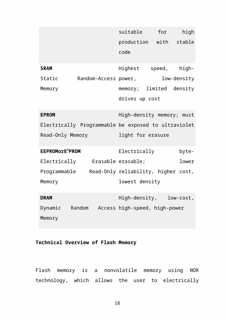
Memory Type
Features
FLASH Low-cost, high-density, high-speed
architecture; low power; high
reliability
ROM
Read-Only Memory
Mature, high-density, reliable, low
cost; time-consuming mask required,
suitable for high production with
stable code
SRAM
Static Random-Access Memory
Highest speed, high-power, low-
density memory; limited density
12
drives up cost
EPROM
Electrically Programmable Read-
Only Memory
High-density memory; must be
exposed to ultraviolet light for
erasure
EEPROMorE2PROM
Electrically Erasable Programmable
Read-Only Memory
Electrically byte-erasable; lower
reliability, higher cost, lowest density
DRAM
Dynamic Random Access Memory
High-density, low-cost, high-speed,
high-power
Technical Overview of Flash Memory
Flash memory is a nonvolatile memory using NOR technology, which allows the
user to electrically program and erase information. Intel® Flash memory uses
memory cells similar to an EPROM, but with a much thinner, precisely grown
oxide between the floating gate and the source (see Figure 2). Flash programming
occurs when electrons are placed on the floating gate. The charge is stored on the
floating gate, with the oxide layer allowing the cell to be electrically erased
through the source. Intel Flash memory is an extremely reliable nonvolatile
memory architecture.
13

Fig 3.7.3: - Pin diagram of AT89C51
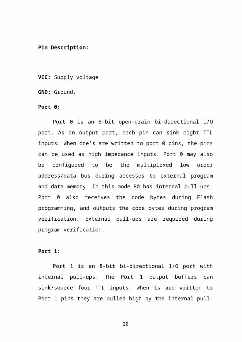
Pin Description:
VCC: Supply voltage.
GND: Ground.
Port 0:
Port 0 is an 8-bit open-drain bi-directional I/O port. As an output port, each
pin can sink eight TTL inputs. When one’s are written to port 0 pins, the pins can
be used as high impedance inputs. Port 0 may also be configured to be the
multiplexed low order address/data bus during accesses to external program and
data memory. In this mode P0 has internal pull-ups. Port 0 also receives the code
14

bytes during Flash programming, and outputs the code bytes during program
verification. External pull-ups are required during program verification.
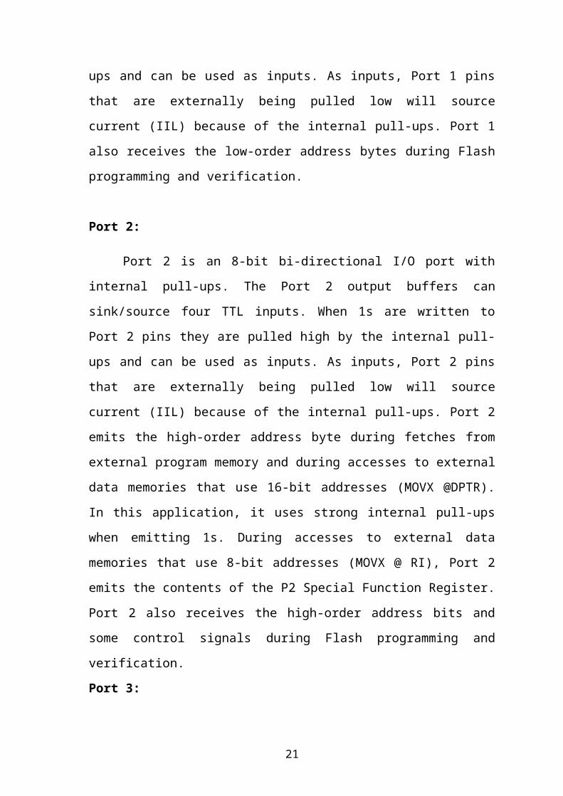
Port 1:
Port 1 is an 8-bit bi-directional I/O port with internal pull-ups. The Port 1
output buffers can sink/source four TTL inputs. When 1s are written to Port 1 pins
they are pulled high by the internal pull-ups and can be used as inputs. As inputs,
Port 1 pins that are externally being pulled low will source current (IIL) because
of the internal pull-ups. Port 1 also receives the low-order address bytes during
Flash programming and verification.
Port 2:
Port 2 is an 8-bit bi-directional I/O port with internal pull-ups. The Port 2
output buffers can sink/source four TTL inputs. When 1s are written to Port 2 pins
they are pulled high by the internal pull-ups and can be used as inputs. As inputs,
Port 2 pins that are externally being pulled low will source current (IIL) because
of the internal pull-ups. Port 2 emits the high-order address byte during fetches
from external program memory and during accesses to external data memories
that use 16-bit addresses (MOVX @DPTR). In this application, it uses strong
internal pull-ups when emitting 1s. During accesses to external data memories that
use 8-bit addresses (MOVX @ RI), Port 2 emits the contents of the P2 Special
Function Register. Port 2 also receives the high-order address bits and some
control signals during Flash programming and verification.
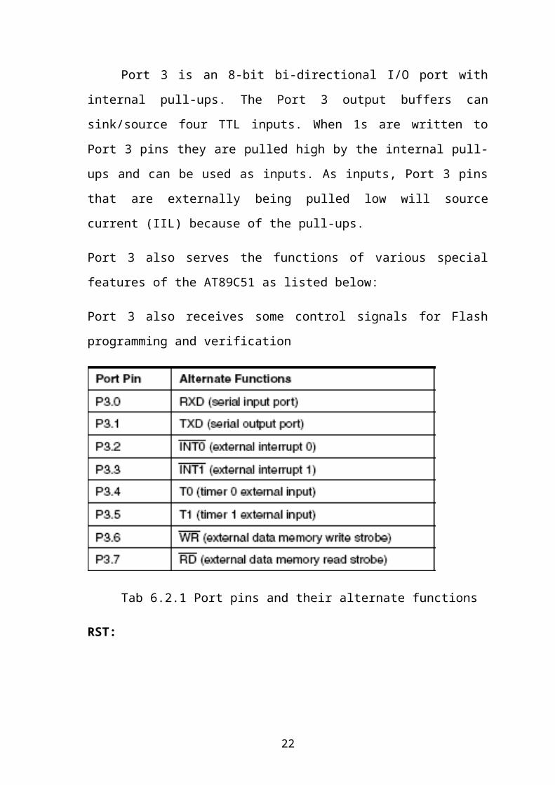
Port 3:
Port 3 is an 8-bit bi-directional I/O port with internal pull-ups. The Port 3
output buffers can sink/source four TTL inputs. When 1s are written to Port 3 pins
they are pulled high by the internal pull-ups and can be used as inputs. As inputs,
Port 3 pins that are externally being pulled low will source current (IIL) because
of the pull-ups.
15
Port 3 also serves the functions of various special features of the AT89C51 as
listed below:
Port 3 also receives some control signals for Flash programming and verification
Tab 6.2.1 Port pins and their alternate functions
RST:
Reset input. A high on this pin for two machine cycles while the oscillator
is running resets the device.
ALE/PROG:
Address Latch Enable output pulse for latching the low byte of the address
during accesses to external memory. This pin is also the program pulse input
(PROG) during Flash programming. In normal operation ALE is emitted at a
constant rate of 1/6the oscillator frequency, and may be used for external timing
or clocking purposes. Note, however, that one ALE pulse is skipped during each
access to external Data Memory.
If desired, ALE operation can be disabled by setting bit 0 of SFR location 8EH.
With the bit set, ALE is active only during a MOVX or MOVC instruction.
Otherwise, the pin is pulled high. Setting the ALE-disable bit has no effect if the
microcontroller is in external execution mode.
16

PSEN:
Program Store Enable is the read strobe to external program memory.
When the AT89C51 is executing code from external program memory, PSEN is
activated twice each machine cycle, except that two PSEN activations are skipped
during each access to external data memory.
EA/VPP:
External Access Enable EA must be strapped to GND in order to enable
the device to fetch code from external program memory locations starting at
0000H up to FFFFH.
Note, however, that if lock bit 1 is programmed, EA will be internally
latched on reset.
EA should be strapped to VCC for internal program executions. This pin also
receives the 12-volt programming enable voltage (VPP) during Flash
programming, for parts that require 12-volt VPP.
XTAL1:
Input to the inverting oscillator amplifier and input to the internal clock
operating circuit.
XTAL2:
It is the Output from the inverting oscillator amplifier.
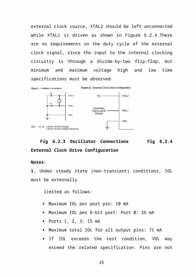
Oscillator Characteristics:
XTAL1 and XTAL2 are the input and output, respectively, of an inverting
amplifier which can be configured for use as an on-chip oscillator, as shown in
Figs 6.2.3. Either a quartz crystal or ceramic resonator may be used. To drive the
device from an external clock source, XTAL2 should be left unconnected while
XTAL1 is driven as shown in Figure 6.2.4.There are no requirements on the duty
cycle of the external clock signal, since the input to the internal clocking circuitry
17
is through a divide-by-two flip-flop, but minimum and maximum voltage high and
low time specifications must be observed.
Fig 6.2.3 Oscillator Connections Fig 6.2.4 External Clock Drive
Configuration
Notes:
1. Under steady state (non-transient) conditions, IOL must be externally
limited as follows:
Maximum IOL per port pin: 10 mA
Maximum IOL per 8-bit port: Port 0: 26 mA
Ports 1, 2, 3: 15 mA
Maximum total IOL for all output pins: 71 mA
If IOL exceeds the test condition, VOL may exceed the related
specification. Pins are not guaranteed to sink current greater than the
listed test conditions.
2. Minimum VCC for Power-down is 2V.
REGISTERS:
In the CPU, registers are used to store information temporarily. That
information could be a byte of data to be processed, or an address pointing to the
data to be fetched. The vast majority of 8051 registers are 8–bit registers. In the
8051 there is only one data type: 8bits. The 8bits of a register are shown in the
diagram from the MSB (most significant bit) D7 to the LSB (least significant bit)
D0. With an 8-bit data type, any data larger than 8bits must be broken into 8-bit
18

chunks before it is processed. Since there are a large number of registers in the
8051, we will concentrate on some of the widely used general-purpose registers
and cover special registers in future chapters.
D7 D6 D5 D4 D3 D2 D1 D0
The most widely used registers of the 8051 are A (accumulator), B, R0,
R1, R2, R3, R4, R5, R6, R7, DPTR (data pointer), and PC (program counter). All
of the above registers are 8-bits, except DPTR and the program counter. The
accumulator, register A, is used for all arithmetic and logic instructions.
SFRs (Special Function Registers)
Among the registers R0-R7 is part of the 128 bytes of RAM memory.
What about registers A, B, PSW, and DPTR? Do they also have addresses? The
answer is yes. In the 8051, registers A, B, PSW and DPTR are part of the group
of registers commonly referred to as SFR (special function registers). There are
many special function registers and they are widely used. The SFR can be
accessed by the names (which is much easier) or by their addresses. For example,
register A has address E0h, and register B has been ignited the address F0H, as
shown in table.
The following two points should noted about the SFR addresses.
1. The Special function registers have addresses between 80H and FFH.
These addresses are above 80H, since the addresses 00 to 7FH are
addresses of RAM memory inside the 8051.
2. Not all the address space of 80H to FFH is used by the SFR. The
unused locations 80H to FFH are reserved and must not be used by the
8051 programmer.
19
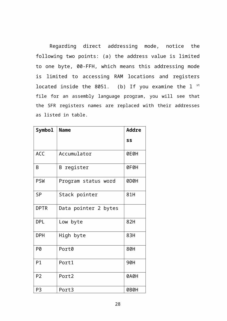
Regarding direct addressing mode, notice the following two points: (a) the
address value is limited to one byte, 00-FFH, which means this addressing mode
is limited to accessing RAM locations and registers located inside the 8051. (b) If
you examine the l st file for an assembly language program, you will see that the SFR
registers names are replaced with their addresses as listed in table.
Symbol Name Address
ACC Accumulator 0E0H
B B register 0F0H
PSW Program status word 0D0H
SP Stack pointer 81H
DPTR Data pointer 2 bytes
DPL Low byte 82H
DPH High byte 83H
P0 Port0 80H
P1 Port1 90H
P2 Port2 0A0H
P3 Port3 0B0H
IP Interrupt priority control 0B8H
IE Interrupt enable control 0A8H
TMOD Timer/counter mode control 89H
TCON Timer/counter control 88H
T2CON Timer/counter 2 control 0C8H
20
T2MOD Timer/counter mode2 control 0C9H
TH0 Timer/counter 0high byte 8CH
TL0 Timer/counter 0 low byte 8AH
TH1 Timer/counter 1 high byte 8DH
TL1 Timer/counter 1 low byte 8BH
TH2 Timer/counter 2 high byte 0CDH
TL2 Timer/counter 2 low byte 0CCH
RCAP2H T/C 2 capture register high byte 0CBH
RCAP2L T/C 2 capture register low byte 0CAH
SCON Serial control 98H
SBUF Serial data buffer 99H
PCON Power control 87H
Table: 8051 Special function register Address
A Register (Accumulator)
This is a general-purpose register which serves for storing intermediate results
during operating. A number (an operand) should be added to the accumulator
prior to execute an instruction upon it. Once an arithmetical operation is
preformed by the ALU, the result is placed into the accumulator. If a data should
be transferred from one register to another, it must go through accumulator. For
21
such universal purpose, this is the most commonly used register that none
microcontroller can be imagined without (more than a half 8051 microcontroller's
instructions used use the accumulator in some way).
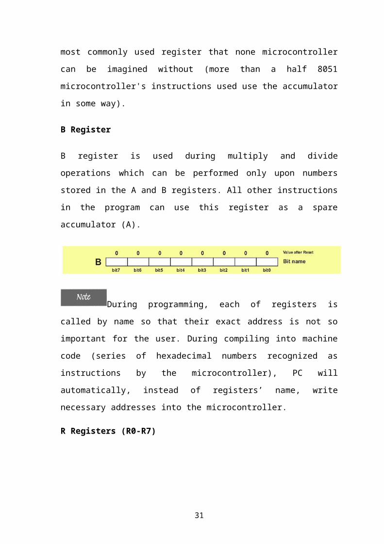
B Register
B register is used during multiply and divide operations which can be performed
only upon numbers stored in the A and B registers. All other instructions in the
program can use this register as a spare accumulator (A).
During programming, each of registers is called by name so that
their exact address is not so important for the user. During compiling into machine
code (series of hexadecimal numbers recognized as instructions by the
microcontroller), PC will automatically, instead of registers’ name, write
necessary addresses into the microcontroller.
R Registers (R0-R7)
22

This is a common name for the total 8 general purpose registers (R0, R1, and
R2 ...R7). Even they are not true SFRs; they deserve to be discussed here because
of their purpose. The bank is active when the R registers it includes are in use.
Similar to the accumulator, they are used for temporary storing variables and
intermediate results. Which of the banks will be active depends on two bits
included in the PSW Register. These registers are stored in four banks in the
scope of RAM.
The following example best illustrates the useful purpose of these registers.
Suppose that mathematical operations on numbers previously stored in the R
registers should be performed: (R1+R2) - (R3+R4). Obviously, a register for
temporary storing results of addition is needed. Everything is quite simple and the
program is as follows:
MOV A, R3; Means: move number from R3 into accumulator
ADD A, R4; Means: add number from R4 to accumulator (result remains in
accumulator)
MOV R5, A; Means: temporarily moves the result from accumulator into R5
MOV A, R1; Means: move number from R1 into accumulator
ADD A, R2; Means: add number from R2 to accumulator
SUBB A, R5; Means: subtract number from R5 (there are R3+R4)
8051 Register Banks and Stack
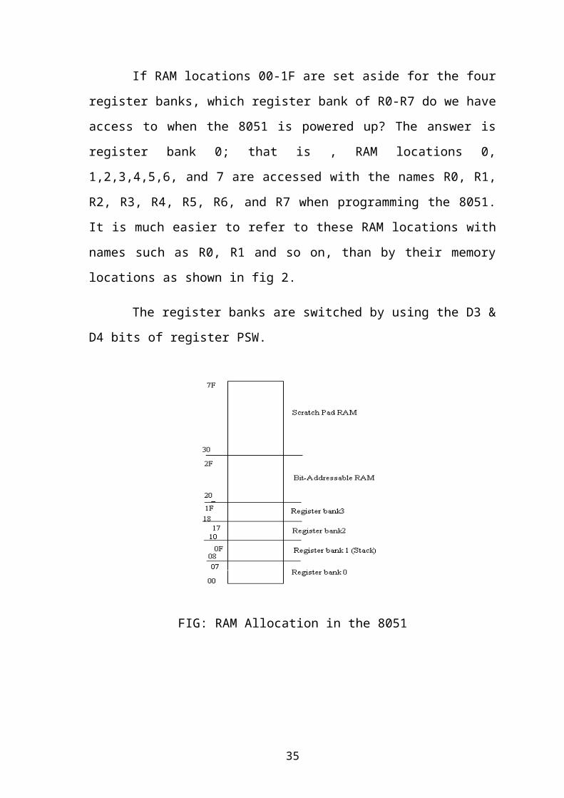
RAM memory space allocation in the 8051
There are 128 bytes of RAM in the 8051. The 128 bytes of RAM inside
the 8051 are assigned addresses 00 to7FH. These 128 bytes are divided into three
different groups as follows:
1. A total of 32 bytes from locations 00 to 1FH hex are set aside for
register banks and the stack.
23
2. A total of 16 bytes from locations 20 to 2FH hex are set aside for bit-
addressable read/write memory.
3. A total of 80 bytes from locations 30H to 7FH are used for read and
write storage, or what is normally called Scratch pad. These 80
locations of RAM are widely used for the purpose of storing data and
parameters nu 8051 programmers.
Register banks in the 8051
A total of 32bytes of RAM are set aside for the register banks and stack.
These 32 bytes are divided into 4 banks of registers in which each bank has
registers, R0-R7. RAM locations 0 to 7 are set aside for bank 0 of R0-R7 where
R0 is RAM location 0, R1 is RAM location 1, and R2 is location 2, and so on,
until memory location7, which belongs to R7 of bank0. The second bank of
registers R0-R7 starts at RAM location 08 and goes to location 0FH. The third
bank of R0-R7 starts at memory location 10H and goes to location 17H. Finally,
RAM locations 18H to 1FH are set aside for the fourth bank of R0-R7. Fig shows
how the 32 bytes are allocated into 4 banks.
As we can see from fig 1, the bank 1 uses the same RAM space as the
stack. This is a major problem in programming the 8051. we must either not use
register bank1, or allocate another area of RAM for the stack.
Default register bank
If RAM locations 00-1F are set aside for the four register banks, which
register bank of R0-R7 do we have access to when the 8051 is powered up? The
answer is register bank 0; that is , RAM locations 0, 1,2,3,4,5,6, and 7 are
accessed with the names R0, R1, R2, R3, R4, R5, R6, and R7 when programming
the 8051. It is much easier to refer to these RAM locations with names such as
R0, R1 and so on, than by their memory locations as shown in fig 2.
24
The register banks are switched by using the D3 & D4 bits of register
PSW.
FIG: RAM Allocation in the 8051
Fig: 8051 Register Banks and their RAM Addresses
25
PSW Register (Program Status Word)
This is one of the most important SFRs. The Program Status Word (PSW)
contains several status bits that reflect the current state of the CPU. This register
contains: Carry bit, Auxiliary Carry, two register bank select bits, Overflow flag,
parity bit, and user-definable status flag. The ALU automatically changes some of
register’s bits, which is usually used in regulation of the program performing.
P - Parity bit. If a number in accumulator is even then this bit will be
automatically set (1), otherwise it will be cleared (0). It is mainly used during data
transmission and receiving via serial communication.
- Bit 1. This bit is intended for the future versions of the microcontrollers, so it is
not supposed to be here.
OV Overflow occurs when the result of arithmetical operation is greater than 255
(decimal), so that it can not be stored in one register. In that case, this bit will be
set (1). If there is no overflow, this bit will be cleared (0).
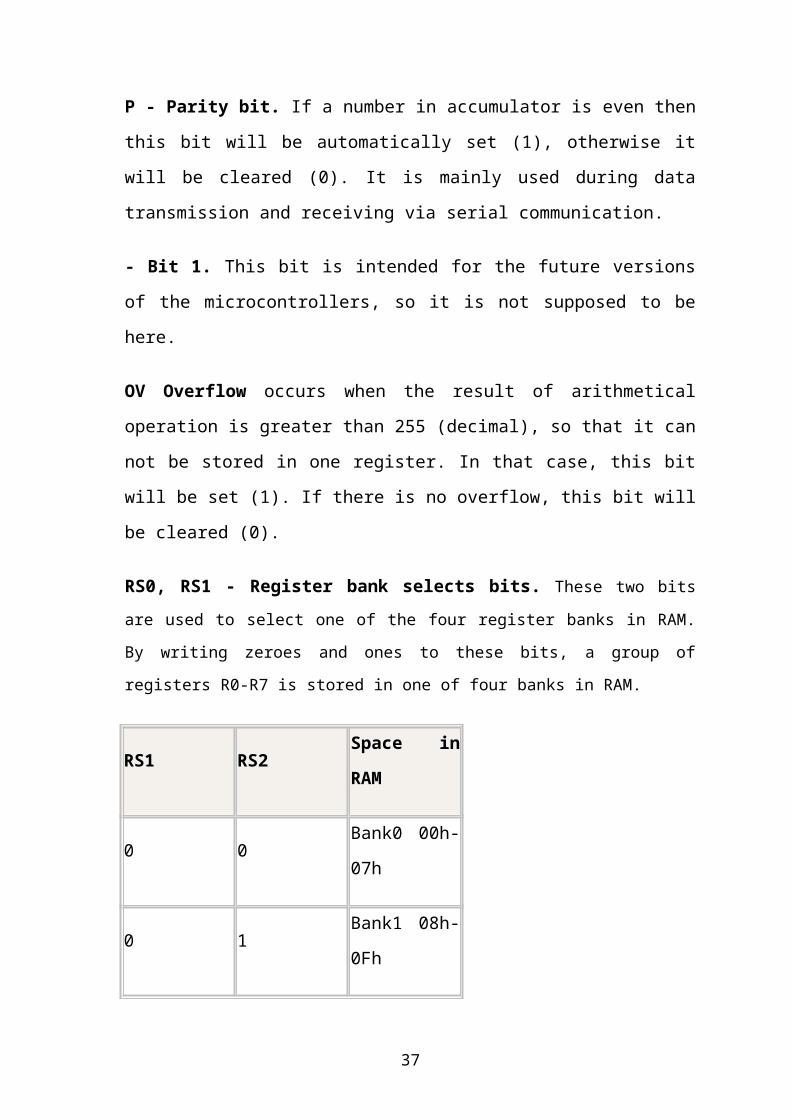
RS0, RS1 - Register bank selects bits. These two bits are used to select one of the
four register banks in RAM. By writing zeroes and ones to these bits, a group of registers
R0-R7 is stored in one of four banks in RAM.
RS1 RS2 Space in RAM
0 0 Bank0 00h-07h
0 1 Bank1 08h-0Fh
1 0 Bank2 10h-17h
26
1 1 Bank3 18h-1Fh
F0 - Flag 0. This is a general-purpose bit available to the user.
AC - Auxiliary Carry Flag is used for BCD operations only.
CY - Carry Flag is the (ninth) auxiliary bit used for all arithmetical operations
and shift instructions.
DPTR Register (Data Pointer)
These registers are not true ones because they do not physically exist. They
consist of two separate registers: DPH (Data Pointer High) and (Data Pointer
Low). Their 16 bits are used for external memory addressing. They may be
handled as a 16-bit register or as two independent 8-bit registers. Besides, the
DPTR Register is usually used for storing data and intermediate results which
have nothing to do with memory locations.
SP Register (Stack Pointer)
27
The stack is a section of RAM used by the CPU to store information
temporarily. This information could be data or an address. The CPU needs this
storage area since there are only a limited number of registers.
How stacks are accessed in the 8051
If the stack is a section of RAM, there must be registers inside the CPU
to point to it. The register used to access the stack is called the SP (Stack point)
Register. The stack pointer in the 8051 is only 8 bits wide; which means that it
can take values of 00 to FFH. When the 8051 is powered up, the SP register
contains value 07. This means that RAM location 08 is the first location used for
the stack by the 8051. The storing of a CPU register in the stack is called a
PUSH, and pulling the contents off the stack back into a CPU register is called a
POP. In other words, a register is pushed onto the stack to save it and popped off
the stack to retrieve it. The job of the SP is very critical when push and pop
actions are performed.
Pushing onto the stack
In the 8051 the stack pointer (SP) points to the last used location of the
stack. As we push data onto the stack, the stack pointer is incremented by one.
Notice that this different from many microprocessors, notably x86 processors in
which the SP is decremented when data is pushed onto the stack. As each PUSH
is executed, the contents of the register are saved on the stack and SP is
incremented by 1. Notice that for every byte of data saved on the stack and then
SP is incremented only once. Notice also that to push the registers onto the stack
we must use their RAM addresses. For example, the instruction “PUSH” pushes
register R1 onto the stack.
28

Popping from the stack
Popping the contents of the stack back into a given register is the opposite
process of pushing. With every pop, the top byte of the stack is copied to the
register specified by the instruction and the stack pointer is decremented once.
The upper limit of the stack
As, mentioned earlier, locations 08 to 1FH in the 8051 RAM can be used
for the stack. This is because locations 20-2FH of RAM are reserved for bit-
addressable memory and must not be used by the stack. If in a program we need
more than 24 bytes (08 to 1FH=24bytes) of stack, we can change the SP to point
to RAM locations 30-7FH. This is done with the instruction “MOV SP, #XX”.
P0, P1, P2, P3 - Input/Output Registers
In case that external memory and serial communication system are not in use then,
4 ports with in total of 32 input-output lines are available to the user for
connection to peripheral environment. Each bit inside these ports corresponds to
the appropriate pin on the microcontroller. This means that logic state written to
these ports appears as a voltage on the pin (0 or 5 V). Naturally, while reading, the
opposite occurs – voltage on some input pins is reflected in the appropriate port
bit.
The state of a port bit, besides being reflected in the pin, determines at the same
time whether it will be configured as input or output. If a bit is cleared (0), the pin
will be configured as output. In the same manner, if a bit is set to 1 the pin will be
configured as input. After reset, as well as when turning the microcontroller ON,
29

all bits on these ports are set to one (1). This means that the appropriate pins will
be configured as inputs.
Program counter:
The important register in the 8051 is the PC (Program counter). The
program counter points to the address of the next instruction to be executed. As
the CPU fetches the OPCODE from the program ROM, the program counter is
incremented to point to the next instruction. The program counter in the 8051 is
16bits wide. This means that the 8051 can access program addresses 0000 to
FFFFH, a total of 64k bytes of code. However, not all members of the 8051 have
the entire 64K bytes of on-chip ROM installed, as we will see soon.
Types of instructions
Depending on operation they perform, all instructions are divided in several
groups:
Arithmetic Instructions
Branch Instructions
Data Transfer Instructions
Logical Instructions
Logical Instructions with bits
The first part of each instruction, called MNEMONIC refers to the operation an
instruction performs (copying, addition, logical operation etc.). Mnemonics
commonly are shortened form of name of operation being executed. For example:
INC R1; Increment R1 (increment register R1)
LJMP LAB5 ;Long Jump LAB5 (long jump to address specified as LAB5)
JNZ LOOP ;Jump if Not Zero LOOP (if the number in the accumulator is not 0,
jump to address specified as LOOP)
30
Another part of instruction, called OPERAND is separated from mnemonic at
least by one empty space and defines data being processed by instructions. Some
instructions have no operand; some have one, two or three. If there is more than
one operand in instruction, they are separated by comma. For example:
RET - (return from sub-routine)
JZ TEMP - (if the number in the accumulator is not 0, jump to address specified
as TEMP)
ADD A,R3 - (add R3 and accumulator)
CJNE A,#20,LOOP - (compare accumulator with 20. If they are not equal, jump
to address specified as LOOP)
Arithmetic instructions
These instructions perform several basic operations (addition, subtraction,
division, multiplication etc.) After execution, the result is stored in the first
operand. For example:
ADD A, R1 - The result of addition (A+R1) will be stored in the accumulator.
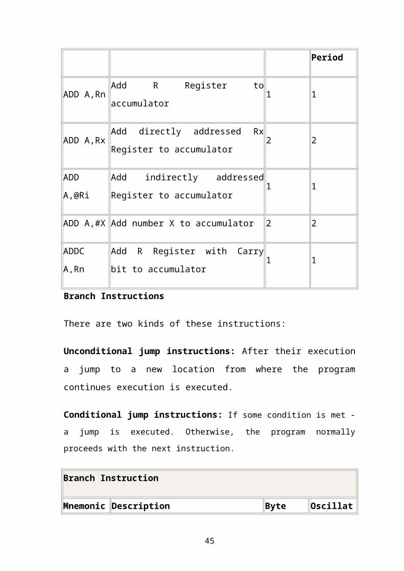
Arithmetical Instructions
Mnemonic DescriptionByte
Number
Oscillator
Period
ADD A,Rn Add R Register to accumulator 1 1
ADD A,RxAdd directly addressed Rx Register to
accumulator2 2
ADD
A,@Ri
Add indirectly addressed Register to
accumulator1 1
ADD A,#X Add number X to accumulator 2 2
31

ADDC
A,Rn
Add R Register with Carry bit to
accumulator1 1
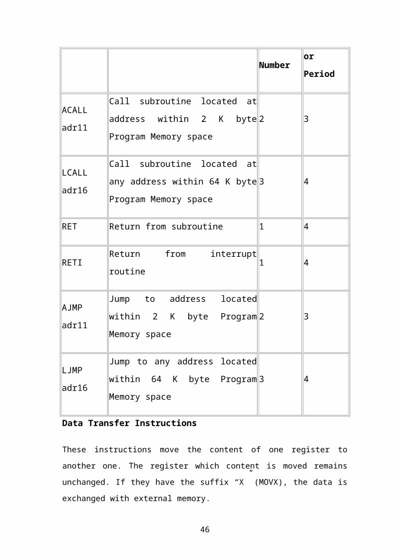
Branch Instructions
There are two kinds of these instructions:
Unconditional jump instructions: After their execution a jump to a new location
from where the program continues execution is executed.
Conditional jump instructions: If some condition is met - a jump is executed.
Otherwise, the program normally proceeds with the next instruction.
Branch Instruction
Mnemonic DescriptionByte
Number
Oscillator
Period
ACALL
adr11
Call subroutine located at address within 2
K byte Program Memory space2 3
LCALL
adr16
Call subroutine located at any address
within 64 K byte Program Memory space3 4
RET Return from subroutine 1 4
RETI Return from interrupt routine 1 4
AJMP adr11Jump to address located within 2 K byte
Program Memory space2 3
LJMP adr16Jump to any address located within 64 K
byte Program Memory space3 4
Data Transfer Instructions
32

These instructions move the content of one register to another one. The register which
content is moved remains unchanged. If they have the suffix “X” (MOVX), the data is
exchanged with external memory.
Data Transfer Instruction
Mnemonic DescriptionByte
Number
Cycle
Number
MOV A,Rn Move R register to accumulator 1 1
MOV A,RxMove directly addressed Rx register to
accumulator2 2
MOV
A,@Ri
Move indirectly addressed register to
accumulator1 1
MOV A,#X Move number X to accumulator 2 2
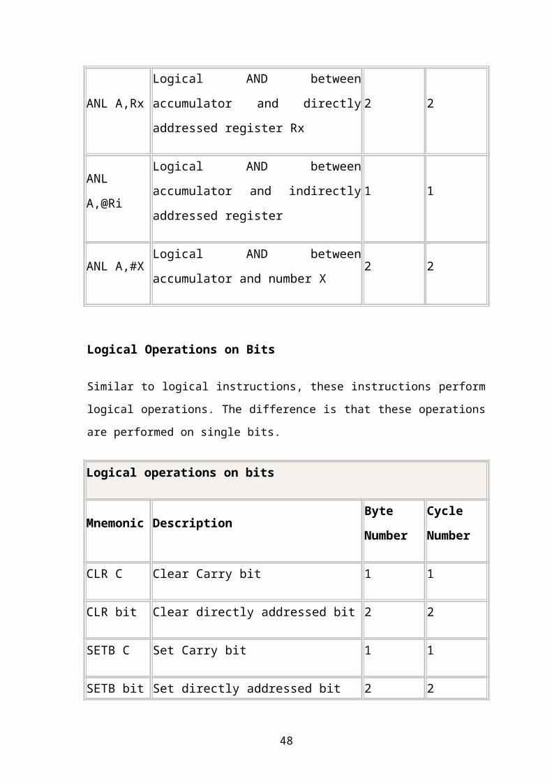
Logical Instructions
These instructions perform logical operations between corresponding bits of two
registers. After execution, the result is stored in the first operand.
Logical Instructions
Mnemonic DescriptionByte
Number
Cycle
Number
ANL A,RnLogical AND between accumulator and R
register1 1
ANL A,Rx Logical AND between accumulator and 2 2
33

directly addressed register Rx
ANL A,@RiLogical AND between accumulator and
indirectly addressed register1 1
ANL A,#XLogical AND between accumulator and
number X2 2
Logical Operations on Bits
Similar to logical instructions, these instructions perform logical operations. The
difference is that these operations are performed on single bits.
Logical operations on bits
Mnemonic DescriptionByte
Number
Cycle
Number
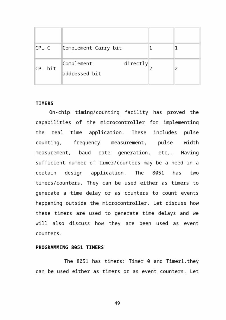
CLR C Clear Carry bit 1 1
CLR bit Clear directly addressed bit 2 2
SETB C Set Carry bit 1 1
SETB bit Set directly addressed bit 2 2
CPL C Complement Carry bit 1 1
CPL bit Complement directly addressed bit 2 2
34
TIMERSOn-chip timing/counting facility has proved the capabilities of the
microcontroller for implementing the real time application. These includes pulse
counting, frequency measurement, pulse width measurement, baud rate
generation, etc,. Having sufficient number of timer/counters may be a need in a
certain design application. The 8051 has two timers/counters. They can be used
either as timers to generate a time delay or as counters to count events happening
outside the microcontroller. Let discuss how these timers are used to generate
time delays and we will also discuss how they are been used as event counters.
PROGRAMMING 8051 TIMERS
The 8051 has timers: Timer 0 and Timer1.they can be used either as timers
or as event counters. Let us first discuss about the timers’ registers and how to
program the timers to generate time delays.
BASIC RIGISTERS OF THE TIMER
Both Timer 0 and Timer 1 are 16 bits wide. Since the 8051 has an 8-bit
architecture, each 16-bit timer is accessed as two separate registers of low byte
and high byte.
TIMER 0 REGISTERS
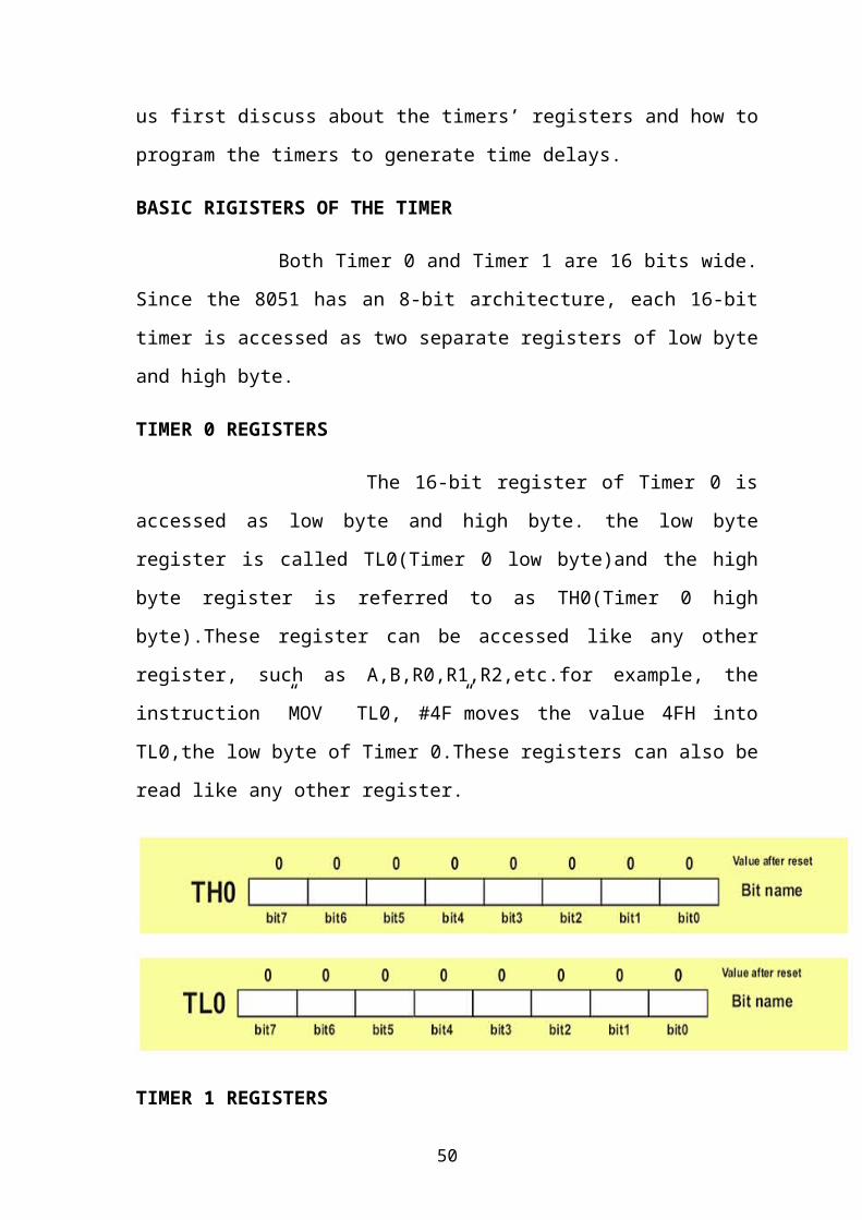
The 16-bit register of Timer 0 is accessed as low byte and high byte. the
low byte register is called TL0(Timer 0 low byte)and the high byte register is
referred to as TH0(Timer 0 high byte).These register can be accessed like any
other register, such as A,B,R0,R1,R2,etc.for example, the instruction ”MOV
TL0, #4F”moves the value 4FH into TL0,the low byte of Timer 0.These registers
can also be read like any other register.
35
TIMER 1 REGISTERS
Timer 1 is also 16-bit register is split into two bytes, referred to as TL1
(Timer 1 low byte) and TH1 (Timer 1 high byte).these registers are accessible n
the same way as the register of Timer 0.
TMOD (timer mode) REGISTER
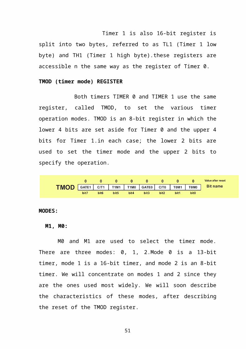
Both timers TIMER 0 and TIMER 1 use the same register, called TMOD,
to set the various timer operation modes. TMOD is an 8-bit register in which the
lower 4 bits are set aside for Timer 0 and the upper 4 bits for Timer 1.in each
case; the lower 2 bits are used to set the timer mode and the upper 2 bits to specify
the operation.
MODES:
M1, M0:
M0 and M1 are used to select the timer mode. There are three modes: 0,
1, 2.Mode 0 is a 13-bit timer, mode 1 is a 16-bit timer, and mode 2 is an 8-bit
timer. We will concentrate on modes 1 and 2 since they are the ones used most
widely. We will soon describe the characteristics of these modes, after describing
the reset of the TMOD register.
36
GATE Gate control when set. The timer/counter is
enabled only
While the INTx pin is high and the TRx control
pin is.
Set. When cleared, the timer is enabled.
C/T Timer or counter selected cleared for timer
operation
(Input from internal system clock).set for
counter
Operation (input TX input pin).
M 1 Mode bit 1
M0 Mode bit 0
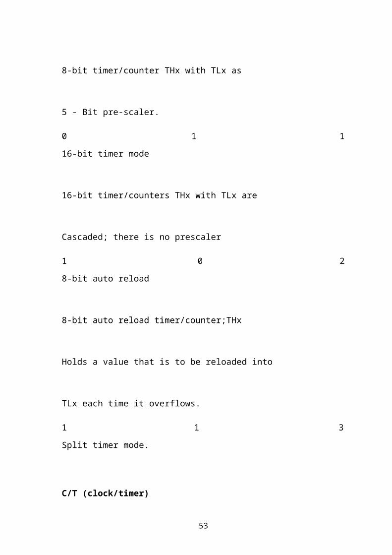
M1 M0 MODE Operating Mode
0 0 0 13-bit timer mode
8-bit timer/counter THx with TLx
as
5 - Bit pre-scaler.
0 1 1 16-bit timer mode
16-bit timer/counters THx with
TLx are
Cascaded; there is no prescaler
37
1 0 2 8-bit auto reload
8-bit auto reload
timer/counter;THx
Holds a value that is to be reloaded
into
TLx each time it overflows.
1 1 3 Split timer mode.
C/T (clock/timer)
This bit in the TMOD register is used to decide whether the timer is used as a
delay generator or an event counter. If C/T=0, it is used as a timer for time delay
generation. The clock source for the time delay is the crystal frequency of the
8051. This section is concerned with this choice. The timer’s use as an event
counter is discussed in the next section.
Serial Communication:
Computers can transfer data in two ways: parallel and serial. In parallel
data transfers, often 8 or more lines (wire conductors) are used to transfer data to a
device that is only a few feet away. Examples of parallel data transfer are printers
and hard disks; each uses cables with many wire strips. Although in such cases a
lot of data can be transferred in a short amount of time by using many wires in
parallel, the distance cannot be great. To transfer to a device located many meters
away, the serial method is used. In serial communication, the data is sent one bit
at a time, in contrast to parallel communication, in which the data is sent a byte or
more at a time. Serial communication of the 8051 is the topic of this chapter. The
38

8051 has serial communication capability built into it, there by making possible
fast data transfer using only a few wires.
If data is to be transferred on the telephone line, it must be converted
from 0s and 1s to audio tones, which are sinusoidal-shaped signals. A peripheral
device called a modem, which stands for “modulator/demodulator”, performs this
conversion.
Serial data communication uses two methods, asynchronous and
synchronous. The synchronous method transfers a block of data at a time, while
the asynchronous method transfers a single byte at a time.
In data transmission if the data can be transmitted and received, it is a
duplex transmission. This is in contrast to simplex transmissions such as with
printers, in which the computer only sends data. Duplex transmissions can be half
or full duplex, depending on whether or not the data transfer can be simultaneous.
If data is transmitted one way at a time, it is referred to as half duplex. If the data
can go both ways at the same time, it is full duplex. Of course, full duplex
requires two wire conductors for the data lines, one for transmission and one for
reception, in order to transfer and receive data simultaneously.
Asynchronous serial communication and data framing
The data coming in at the receiving end of the data line in a serial data
transfer is all 0s and 1s; it is difficult to make sense of the data unless the sender
and receiver agree on a set of rules, a protocol, on how the data is packed, how
many bits constitute a character, and when the data begins and ends.
Start and stop bits
Asynchronous serial data communication is widely used for character-
oriented transmissions, while block-oriented data transfers use the synchronous
method. In the asynchronous method, each character is placed between start and
stop bits. This is called framing. In the data framing for asynchronous
communications, the data, such as ASCII characters, are packed between a start
39

bit and a stop bit. The start bit is always one bit, but the stop bit can be one or two
bits. The start bit is always a 0 (low) and the stop bit (s) is 1 (high).
Data transfer rate
The rate of data transfer in serial data communication is stated in bps
(bits per second). Another widely used terminology for bps is baud rate.
However, the baud and bps rates are not necessarily equal. This is due to the fact
that baud rate is the modem terminology and is defined as the number of signal
changes per second. In modems a single change of signal, sometimes transfers
several bits of data. As far as the conductor wire is concerned, the baud rate and
bps are the same, and for this reason we use the bps and baud interchangeably.
The data transfer rate of given computer system depends on
communication ports incorporated into that system. For example, the early
IBMPC/XT could transfer data at the rate of 100 to 9600 bps. In recent years,
however, Pentium based PCS transfer data at rates as high as 56K bps. It must be
noted that in asynchronous serial data communication, the baud rate is generally
limited to 100,000bps.
RS232 Standards
To allow compatibility among data communication equipment made by
various manufacturers, an interfacing standard called RS232 was set by the
Electronics Industries Association (EIA) in 1960. In 1963 it was modified and
called RS232A. RS232B AND RS232C were issued in 1965 and 1969,
respectively. Today, RS232 is the most widely used serial I/O interfacing
standard. This standard is used in PCs and numerous types of equipment.
However, since the standard was set long before the advert of the TTL logic
family, its input and output voltage levels are not TTL compatible. In RS232, a 1
is represented by -3 to -25V, while a 0 bit is +3 to +25V, making -3 to +3
undefined. For this reason, to connect any RS232 to a microcontroller system we
must use voltage converters such as MAX232 to convert the TTL logic levels to
40

the RS232 voltage levels, and vice versa. MAX232 IC chips are commonly
referred to as line drivers.
RS232 pins
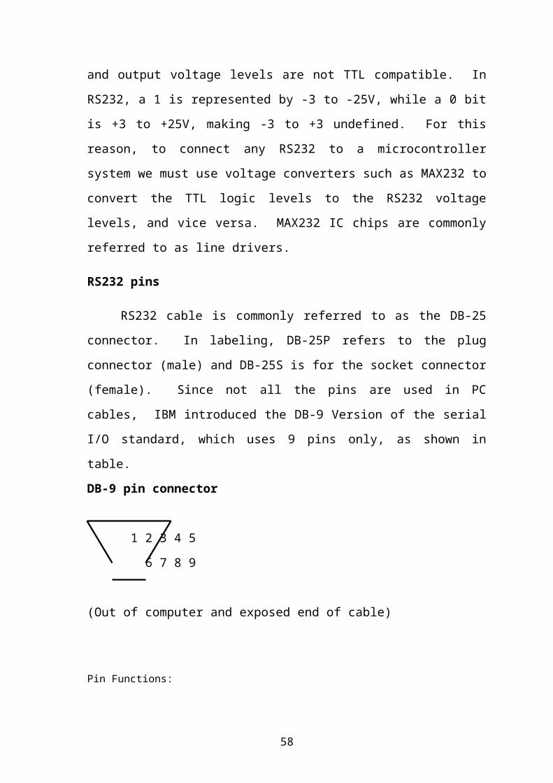
RS232 cable is commonly referred to as the DB-25 connector. In labeling,
DB-25P refers to the plug connector (male) and DB-25S is for the socket
connector (female). Since not all the pins are used in PC cables, IBM introduced
the DB-9 Version of the serial I/O standard, which uses 9 pins only, as shown in
table.
DB-9 pin connector
1 2 3 4 5
6 7 8 9
(Out of computer and exposed end of cable)
Pin Functions:
Pin Description
1 Data carrier detect (DCD)
2 Received data (RXD)
3 Transmitted data (TXD)
4 Data terminal ready(DTR)
5 Signal ground (GND)
6 Data set ready (DSR)
7 Request to send (RTS)
8 Clear to send (CTS)
9 Ring indicator (RI)
Note: DCD, DSR, RTS and CTS are active low pins.
41

The method used by RS-232 for communication allows for a simple connection
of three lines: Tx, Rx, and Ground. The three essential signals for 2-way RS-232
Communications are these:
TXD: carries data from DTE to the DCE.
RXD: carries data from DCE to the DTE
SG: signal ground
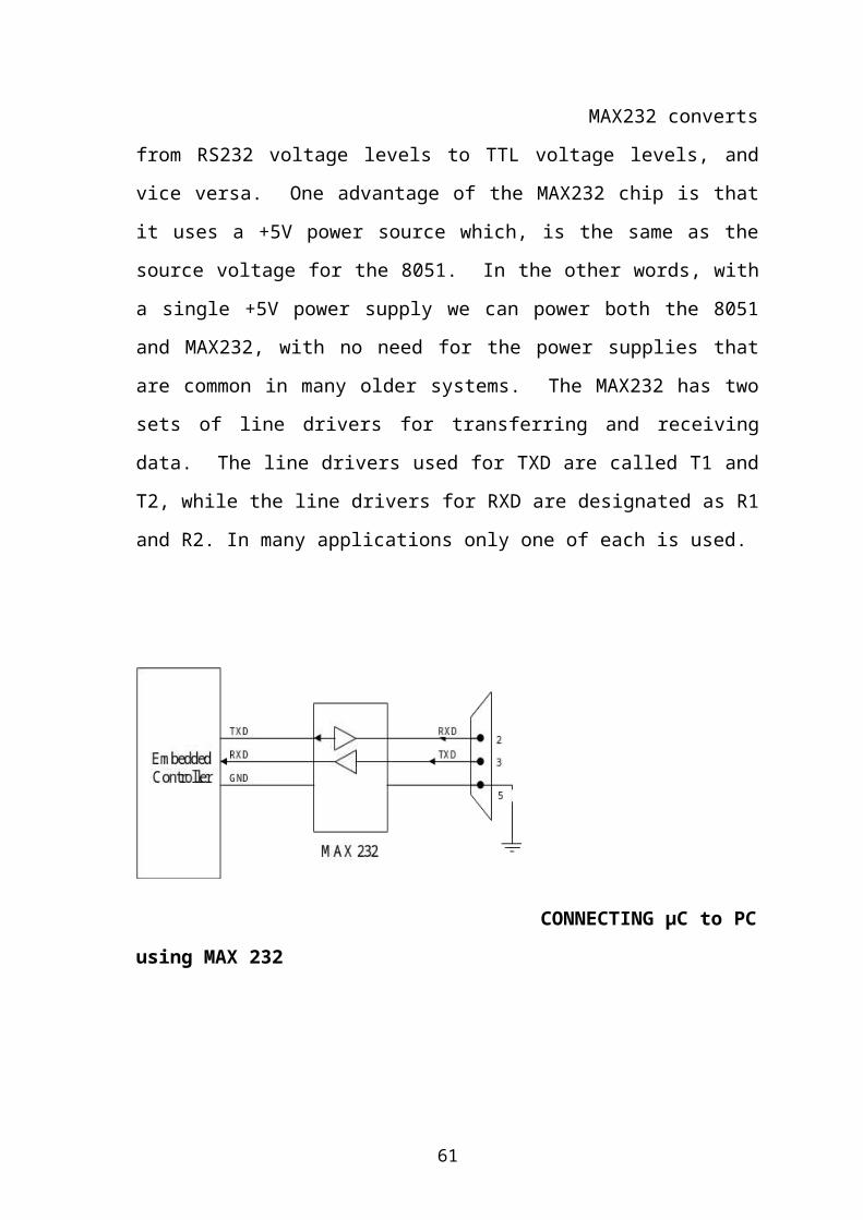
8051 connection to RS232
The RS232 standard is not TTL compatible; therefore, it requires a line
driver such as the MAX232 chip to convert RS232 voltage levels to TTL levels,
and vice versa. The interfacing of 8051 with RS232 connectors via the MAX232
chip is the main topic.
The 8051 has two pins that are used specifically for transferring
and receiving data serially. These two pins are called TXD and RXD and a part of
the port 3 group (P3.0 and P3.1). Pin 11 of the 8051 is assigned to TXD and pin
10 is designated as RXD. These pins are TTL compatible; therefore, they require
a line driver to make them RS232 compatible. One such line driver is the
MAX232 chip.
MAX232 converts from RS232 voltage levels to TTL
voltage levels, and vice versa. One advantage of the MAX232 chip is that it uses
a +5V power source which, is the same as the source voltage for the 8051. In the
other words, with a single +5V power supply we can power both the 8051 and
MAX232, with no need for the power supplies that are common in many older
systems. The MAX232 has two sets of line drivers for transferring and receiving
42
data. The line drivers used for TXD are called T1 and T2, while the line drivers
for RXD are designated as R1 and R2. In many applications only one of each is
used.
CONNECTING μC to PC using MAX 232
INTERRUPTSA single microcontroller can serve several devices. There are two ways to do that:
INTERRUPTS or POLLING.
POLLING:
In polling the microcontroller continuously monitors the status of a given device;
when the status condition is met, it performs the service .After that, it moves on to
monitor the next device until each one is serviced. Although polling can monitor
the status of several devices and serve each of them as certain condition are met.
43
INTERRUPTS:
In the interrupts method, whenever any device needs its
service, the device notifies the microcontroller by sending it an interrupts signal.
Upon receiving an interrupt signal, the microcontroller interrupts whatever it is
doing and serves the device. The program associated with the interrupts is called
the interrupt service routine (ISR).or interrupt handler.
INTERRUPTS Vs POLLING:
The advantage of interrupts is that the microcontroller can serve many
devices (not all the same time, of course); each device can get the attention of
the microcontroller based on the priority assigned to it. The polling method
cannot assign priority since it checks all devices in round-robin fashion. More
importantly, in the interrupt method the microcontroller can also ignore (mask)
a device request for service. This is again not possible with the polling
method. The most important reason that the interrupt method is preferable is
that the polling method wastes much of the microcontroller’s time by polling
devices that do not need service. So, in order to avoid tying down the
microcontroller, interrupts are used.
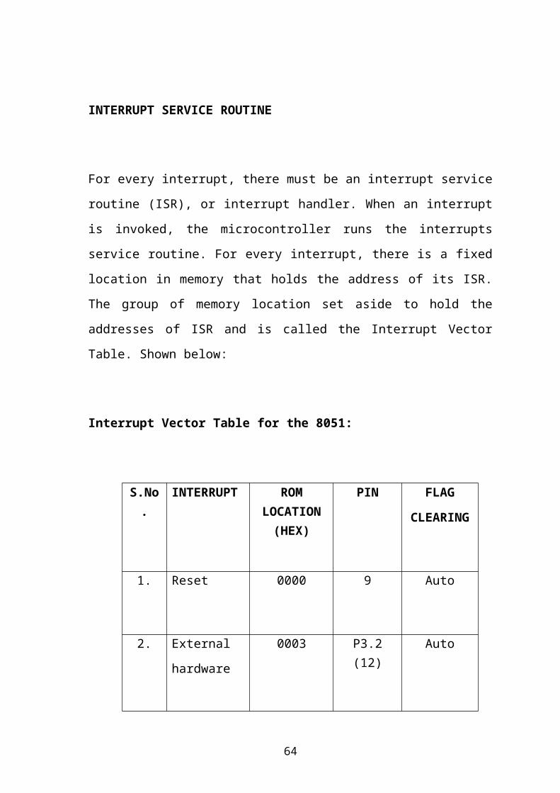
INTERRUPT SERVICE ROUTINE
44
For every interrupt, there must be an interrupt service routine (ISR), or interrupt
handler. When an interrupt is invoked, the microcontroller runs the interrupts
service routine. For every interrupt, there is a fixed location in memory that holds
the address of its ISR. The group of memory location set aside to hold the
addresses of ISR and is called the Interrupt Vector Table. Shown below:
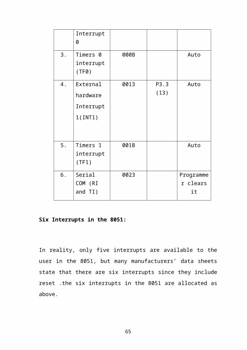
Interrupt Vector Table for the 8051:
S.No. INTERRUPT ROM LOCATION
(HEX)
PIN FLAG
CLEARING
1. Reset 0000 9 Auto
2. External
hardware
Interrupt 0
0003 P3.2 (12) Auto
3. Timers 0 interrupt (TF0)
000B Auto
4. External
hardware
Interrupt
1(INT1)
0013 P3.3 (13) Auto
5. Timers 1 interrupt (TF1)
001B Auto
45
6. Serial COM (RI and TI)
0023 Programmer clears it
Six Interrupts in the 8051:
In reality, only five interrupts are available to the user in the 8051, but many
manufacturers’ data sheets state that there are six interrupts since they include
reset .the six interrupts in the 8051 are allocated as above.
1. Reset. When the reset pin is activated, the 8051 jumps to address location
0000.this is the power-up reset.
2. Two interrupts are set aside for the timers: one for Timer 0 and one for
Timer 1.Memory location 000BH and 001BH in the interrupt vector table
belong to Timer 0 and Timer 1, respectively.
3. Two interrupts are set aside for hardware external harder interrupts. Pin
number 12(P3.2) and 13(P3.3) in port 3 are for the external hardware
interrupts INT0 and INT1,respectively.These external interrupts are also
referred to as EX1 and EX2.Memory location 0003H and 0013H in the
interrupt vector table are assigned to INT0 and INT1, respectively.
4. Serial communication has a single interrupt that belongs to both receive
and transmit. The interrupt vector table location 0023H belongs to this
interrupt.
Notice that a limited number of bytes are set aside for each interrupt. For example,
a total of 8 bytes from location 0003 to 000A is set aside for INT0, external
hardware interrupt 0.similarly,a total of 8 bytes from location 00BH to 0012H is
reserved for TF0, Timer 0 interrupt. If the service routine for a given interrupt is
short enough to fit in the memory space allocated to it, it is placed in the vector
table; otherwise, and an LJMP instruction is placed in the vector table to point to
the address of the ISR. In that rest of the bytes allocated to that interrupt are
unused.
46

From the above table also notice that only three bytes of ROM space are assigned
to the reset pin. they are ROM address location 0,1 and2.address location 3
belongs to external hardware interrupt 0.for this reason, in our program we put
the LJMP as the first instruction and redirect the processor away from the
interrupt vector table, as shown below
Steps in executing an interrupt
Upon activation of an interrupt, the microcontroller goes through the following
steps.
1. It finishes the instruction it is executing and saves the address of the next
instruction (PC) on the stack.
2. It also saves the current status of all the interrupts internally (i.e., not on the
stack).
3. It jumps to a fixed location in memory called the interrupt vector table that
holds the address of the interrupts service routine.
4. The microcontroller gets the address of the ISR from the interrupt vector
table and jumps to it. It starts to execute the interrupt service subroutine
until it reaches the last instruction of the subroutine, which is RETI (return
from interrupt).
5. Upon executing the RETI instruction, the microcontroller returns to the
place where it was interrupted. First, it gets the program counter (PC)
address from the stack by popping the top two bytes of the stack into the
PC. Then it starts to execute from that address.
Notice from step 5 the critical role of the stack. For this reason, we must be
careful in manipulating the stack contents in the ISR. Specifically, in the ISR, just
as in any CALL subroutine, the number of pushes and pops must be equal.
Enabling and disabling an interrupt:
Upon reset, all interrupt are disabled (masked), meaning that none will be
responded to by the microcontroller if they are activated. The interrupt must be
enabled by software in order for the microcontroller to respond to them. There is a
47
register called IE (interrupt enable) that is responsible for enabling (unmasking)
and disabling (masking) the interrupts.
Notice that IE is a bit-addressable register.
Steps in enabling an interrupt:
To enable an interrupt, we take the following steps:
1. Bit D7 of the IE register (EA) must be set to high to allow the reset to take
effect.
If EA=1, interrupts are enabled and will be responded to if their corresponding bit
in IE are high. If EA=0, no interrupt will be responded to, even if the associated
bit in the IE register is high.
Interrupt Enable Register
D7 D6 D5 D4 D3 D2 D1 D0
EA IE.7 disables all interrupts. If EA=0, no interrupts is
acknowledged.
If EA=1, each interrupt source is individually enabled
disabled
By setting or clearing its enable bit.
-- IE.6 Not implemented, reserved for future use.*
ET2 IE.5 Enables or disables Timer 2 overflow or capture interrupt
(8052
Only)
48
EA -- ET2 ES ET1 EX1 ET0 EX0
ES IE.4 Enables or disables the serial port interrupts.
ET1 IE.3 Enables or disables Timers 1 overflow interrupt
EX1 IE.2 Enables or disables external interrupt 1.
ET0 IE.1 Enables or disables Timer 0 overflow interrupt.
EX0 IE.0 Enables or disables external interrupt.
Power supply
The power supplies are designed to convert high voltage
AC mains electricity to a suitable low voltage supply for electronics circuits and
other devices. A power supply can by broken down into a series of blocks, each of
which performs a particular function. A d.c power supply which maintains the
output voltage constant irrespective of a.c mains fluctuations or load variations is
known as “Regulated D.C Power Supply”
For example a 5V regulated power supply system as shown below:
49
Transformer:
A transformer is an electrical device which is used to convert electrical power from one Electrical circuit to another without change in frequency.
Transformers convert AC electricity from one voltage to another with little
loss of power. Transformers work only with AC and this is one of the reasons why
mains electricity is AC. Step-up transformers increase in output voltage, step-
down transformers decrease in output voltage. Most power supplies use a step-
down transformer to reduce the dangerously high mains voltage to a safer low
voltage. The input coil is called the primary and the output coil is called the
secondary. There is no electrical connection between the two coils; instead they
are linked by an alternating magnetic field created in the soft-iron core of the
transformer. The two lines in the middle of the circuit symbol represent the core.
Transformers waste very little power so the power out is (almost) equal to the
power in. Note that as voltage is stepped down current is stepped up. The ratio of
50
the number of turns on each coil, called the turn’s ratio, determines the ratio of the
voltages. A step-down transformer has a large number of turns on its primary
(input) coil which is connected to the high voltage mains supply, and a small
number of turns on its secondary (output) coil to give a low output voltage.
An Electrical Transformer
Turns ratio = Vp/ VS = Np/NS
Power Out= Power In
VS X IS=VP X IP
Vp = primary (input) voltage
Np = number of turns on primary coil
Ip = primary (input) current
RECTIFIER:
A circuit which is used to convert a.c to dc is known as RECTIFIER. The process of conversion a.c to d.c is called “rectification”
51

TYPES OF RECTIFIERS:
Half wave Rectifier Full wave rectifier
1. Centre tap full wave rectifier.
2. Bridge type full bridge rectifier.
Comparison of rectifier circuits:
Parameter
Type of Rectifier
Half wave Full wave Bridge
Number of diodes
1
2
4
PIV of diodes
Vm
2Vm
Vm
D.C output voltage
Vm/
2Vm/
2Vm/
Vdc,at
no-load
0.318Vm
0.636Vm 0.636Vm
Ripple factor
1.21
0.482
0.482
Ripple
frequency
f
2f
2f
Rectification
efficiency
0.406
0.812
0.812
52
Transformer
Utilization
Factor(TUF)
0.287 0.693 0.812
RMS voltage Vrms Vm/2 Vm/√2 Vm/√2
Full-wave Rectifier:
From the above comparision we came to know that full wave bridge rectifier as more advantages than the other two rectifiers. So, in our project we are using full wave bridge rectifier circuit.
Bridge Rectifier: A bridge rectifier makes use of four diodes in a bridge
arrangement to achieve full-wave rectification. This is a widely used
configuration, both with individual diodes wired as shown and with single
component bridges where the diode bridge is wired internally.
A bridge rectifier makes use of four diodes in a bridge arrangement as
shown in fig(a) to achieve full-wave rectification. This is a widely used
configuration, both with individual diodes wired as shown and with single
component bridges where the diode bridge is wired internally.
Fig(A)
53
Operation:
During positive half cycle of secondary, the diodes D2 and D3 are in forward
biased while D1 and D4 are in reverse biased as shown in the fig(b). The current
flow direction is shown in the fig (b) with dotted arrows.
Fig(B)
During negative half cycle of secondary voltage, the diodes D1 and D4 are in
forward biased while D2 and D3 are in reverse biased as shown in the fig(c). The
current flow direction is shown in the fig (c) with dotted arrows.
Fig(C)
Filter:
54

A Filter is a device which removes the a.c component of rectifier output
but allows the d.c component to reach the load
Capacitor Filter:
We have seen that the ripple content in the rectified output of half wave
rectifier is 121% or that of full-wave or bridge rectifier or bridge rectifier is 48%
such high percentages of ripples is not acceptable for most of the applications.
Ripples can be removed by one of the following methods of filtering.
(a) A capacitor, in parallel to the load, provides an easier by –pass for the ripples
voltage though it due to low impedance. At ripple frequency and leave the d.c.to
appears the load.
(b) An inductor, in series with the load, prevents the passage of the ripple current
(due to high impedance at ripple frequency) while allowing the d.c (due to low
resistance to d.c)
(c) various combinations of capacitor and inductor, such as L-section filter
section filter, multiple section filter etc. which make use of both the properties
mentioned in (a) and (b) above. Two cases of capacitor filter, one applied on half
wave rectifier and another with full wave rectifier.
55
Filtering is performed by a large value electrolytic capacitor connected
across the DC supply to act as a reservoir, supplying current to the output when
the varying DC voltage from the rectifier is falling. The capacitor charges quickly
near the peak of the varying DC, and then discharges as it supplies current to the
output. Filtering significantly increases the average DC voltage to almost the peak
value (1.4 × RMS value).
To calculate the value of capacitor(C),
C = ¼*√3*f*r*Rl
Where,
f = supply frequency,
r = ripple factor,
Rl = load resistance
Note: In our circuit we are using 1000µF Hence large value of capacitor is
placed to reduce ripples and to improve the DC component.
Regulator:
Voltage regulator ICs is available with fixed (typically 5, 12 and 15V) or variable
output voltages. The maximum current they can pass also rates them. Negative
voltage regulators are available, mainly for use in dual supplies. Most regulators
include some automatic protection from excessive current ('overload protection')
and overheating ('thermal protection'). Many of the fixed voltage regulator ICs
have 3 leads and look like power transistors, such as the 7805 +5V 1A regulator
shown on the right. The LM7805 is simple to use. You simply connect the
positive lead of your unregulated DC power supply (anything from 9VDC to
24VDC) to the Input pin, connect the negative lead to the Common pin and then
when you turn on the power, you get a 5 volt supply from the output pin.
56

Fig 6.1.6 A Three Terminal Voltage Regulator
78XX:
The Bay Linear LM78XX is integrated linear positive regulator with three
terminals. The LM78XX offer several fixed output voltages making them useful
in wide range of applications. When used as a zener diode/resistor combination
replacement, the LM78XX usually results in an effective output impedance
improvement of two orders of magnitude, lower quiescent current. The LM78XX
is available in the TO-252, TO-220 & TO-263packages
Features:
• Output Current of 1.5A
• Output Voltage Tolerance of 5%
• Internal thermal overload protection
• Internal Short-Circuit Limited
• No External Component
• Output Voltage 5.0V, 6V, 8V, 9V, 10V,12V, 15V, 18V, 24V
• Offer in plastic TO-252, TO-220 & TO-263
• Direct Replacement for LM78XX
LINEAR KEYPAD
57
This section basically consists of a Linear Keypad. Basically a Keypad can be
classified into 2 categories. One is Linear Keypad and the other is Matrix keypad.
1. Matrix Keypad.
2. Linear Keypad.
1. Matrix Keypad: This Keypad got keys arranged in the form of Rows and
Columns. That is why the name Matrix Keypad. According to this keypad,
In order to find the key being pressed the keypad need to be scanned by
making rows as i/p and columns as output or vice versa.
This Keypad is used in places where one needs to connect
more no. of keys with less no. of data lines.
2. Linear Keypad: This Keypad got ‘n’ no. of keys connected to ‘n’ data
lines of microcontroller.
This Keypad is used in places where one needs to connect
less no. of keys.
Generally, in Linear Keypads one end of the switch is connected to
Microcontroller (Configured as i/p) and other end of the switch is connected to
the common ground. So whenever a key of Linear Keypad is pressed the logic
on the microcontroller pin will go LOW.
Here in this project, a linear keypad is used with switches connected in a
serial manner. Linear keypad is used in this project because it takes less no. of
port pins. The Linear Keypad with 4 Keys is shown below.
58

MAX-232:
The MAX232 from Maxim was the first IC which in one package contains the necessary drivers (two) and receivers (also two), to adapt the RS-232 signal voltage levels to TTL logic. It became popular, because it just needs one voltage (+5V) and generates the necessary RS-232 voltage levels (approx. -10V and +10V) internally. This greatly simplified the design of circuitry. Circuitry designers no longer need to design and build a power supply with three voltages (e.g. -12V, +5V, and +12V), but could just provide one +5V power supply, e.g. with the help of a simple 78x05 voltage converter.
The MAX232 has a successor, the MAX232A. The ICs are almost identical, however, the MAX232A is much more often used (and easier to get) than the original MAX232, and the MAX232A only needs external capacitors 1/10th the capacity of what the original MAX232 needs.
It should be noted that the MAX 232(A) is just a driver/receiver. It does not generate the necessary RS-232 sequence of marks and spaces with the right timing, it does not decode the RS-232 signal, it does not provide a serial/parallel conversion. All it does is to convert signal voltage levels. Generating serial data
59
with the right timing and decoding serial data has to be done by additional circuitry, e.g. by a 16550 UART or one of these small micro controllers (e.g. Atmel AVR, Microchip PIC) getting more and more popular.
The MAX232 and MAX232A were once rather expensive ICs, but today they are cheap. It has also helped that many companies now produce clones (ie. Sipex). These clones sometimes need different external circuitry, e.g. the capacities of the external capacitors vary. It is recommended to check the data sheet of the particular manufacturer of an IC instead of relying on Maxim's original data sheet.
The original manufacturer (and now some clone manufacturers, too) offers a large series of similar ICs, with different numbers of receivers and drivers, voltages, built-in or external capacitors, etc. E.g. The MAX232 and MAX232A need external capacitors for the internal voltage pump, while the MAX233 has these capacitors built-in. The MAX233 is also between three and ten times more expensive in electronic shops than the MAX232A because of its internal capacitors. It is also more difficult to get the MAX233 than the garden variety MAX232A.
A Typical Application
The MAX 232(A) has two receivers (converts from RS-232 to TTL voltage levels) and two drivers (converts from TTL logic to RS-232 voltage levels). This means only two of the RS-232 signals can be converted in each direction. The old MC1488/1498 combo provided four drivers and receivers.
Typically a pair of a driver/receiver of the MAX232 is used for
TX and RX
And the second one for
CTS and RTS.
There are not enough drivers/receivers in the MAX232 to also connect the DTR, DSR, and DCD signals. Usually these signals can be omitted when e.g. communicating with a PC's serial interface. If the DTE really requires these signals either a second MAX232 is needed, or some other IC from the MAX232 family can be used (if it can be found in consumer electronic shops at all). An alternative for DTR/DSR is also given below.
Maxim's data sheet explains the MAX232 family in great detail, including the pin configuration and how to connect such an IC to external circuitry. This information can be used as-is in own design to get a working RS-232 interface. Maxim's data just misses one critical piece of information: How exactly to connect the RS-232 signals to the IC. So here is one possible example:
60
MAX232 to RS232 DB9 Connection as a DCE
MAX232 Pin Nbr. MAX232 Pin Name Signal Voltage DB9 Pin
7 T2out CTS RS-232 7
8 R2in RTS RS-232 8
9 R2out RTS TTL n/a
10 T2in CTS TTL n/a
11 T1in TX TTL n/a
12 R1out RX TTL n/a
13 R1in TX RS-232 3
14 T1out RX RS-232 2
15 GND GND 0 5
In addition one can directly wire DTR (DB9 pin 4) to DSR (DB9 pin 6) without going through any circuitry. This gives automatic (brain dead) DSR acknowledgment of an incoming DTR signal.
Sometimes pin 6 of the MAX232 is hard wired to DCD (DB9 pin 1). This is not recommended. Pin 6 is the raw output of the voltage pump and inverter for the -10V voltage. Drawing currents from the pin leads to a rapid breakdown of the voltage, and as a consequence to a breakdown of the output voltage of the two RS-232 drivers. It is better to use software which doesn't care about DCD, but does hardware-handshaking via CTS/RTS only.
The circuitry is completed by connecting five capacitors to the IC as it follows. The MAX232 needs 1.0µF capacitors, the MAX232A needs 0.1µF capacitors. MAX232 clones show similar differences. It is recommended to consult the corresponding data sheet. At least 16V capacitor types should be used. If electrolytic or tantalic capacitors are used, the polarity has to be observed. The first pin as listed in the following table is always where the plus pole of the capacitor should be connected to.
61

MAX232(A) external Capacitors
Capacitor + Pin - Pin Remark
C1 1 3
C2 4 5
C3 2 16
C4 GND 6This looks non-intuitive, but because pin 6 ison -10V, GND gets the + connector, and not the -
C5 16 GND
The 5V power supply is connected to
+5V: Pin 16 GND: Pin 15
Features
Meet or Exceed TIA/EIA-232-F and ITURecommendation V.28
Operate With Single 5-V Power Supply Operate Up to 120 kbit/s Two Drivers and Two Receivers 30-V Input Levels Low Supply Current . . . 8 mA Typical Designed to be Interchangeable WithMaxim MAX232
ESD Protection Exceeds JESD 22 2000-V Human-Body Model (A114-A)
62
ApplicationsTIA/EIA-232-F
Battery-Powered Systems
Terminals
Modems
Computers
Description/ordering information
The MAX232 is a dual driver/receiver that includes a capacitive voltage generator to supply EIA-232 voltage levels from a single 5-V supply. Each receiver converts EIA-232 inputs to 5-V TTL/CMOS levels. These receivers have a typical threshold of 1.3 V and a typical hysteresis of 0.5 V, and can accept 30-V inputs. Each driver converts TTL/CMOS input levels into EIA-232 levels. The driver, receiver, and voltage-generator functions are available as cells in the Texas Instruments Lin ASIClibrary.
63
64
65

66

67

Liquid crystal display
68

Liquid crystal displays (LCDs) have materials, which combine the
properties of both liquids and crystals. Rather than having a melting point, they
have a temperature range within which the molecules are almost as mobile as they
would be in a liquid, but are grouped together in an ordered form similar to a
crystal.
An LCD consists of two glass panels, with the liquid crystal material sand
witched in between them. The inner surface of the glass plates are coated with
transparent electrodes which define the character, symbols or patterns to be
displayed polymeric layers are present in between the electrodes and the liquid
crystal, which makes the liquid crystal molecules to maintain a defined orientation
angle.
One each polarisers are pasted outside the two glass panels. These
polarisers would rotate the light rays passing through them to a definite angle, in a
particular direction.
When the LCD is in the off state, light rays are rotated by the two
polarisers and the liquid crystal, such that the light rays come out of the LCD
without any orientation, and hence the LCD appears transparent.
When sufficient voltage is applied to the electrodes, the liquid crystal
molecules would be aligned in a specific direction. The light rays passing through
the LCD would be rotated by the polarisers, which would result in activating/
highlighting the desired characters.
The LCD’s are lightweight with only a few millimeters thickness. Since the
LCD’s consume less power, they are compatible with low power electronic
circuits, and can be powered for long durations.
The LCD’s don’t generate light and so light is needed to read the display.
By using backlighting, reading is possible in the dark. The LCD’s have long life
and a wide operating temperature range.
69

Changing the display size or the layout size is relatively simple which
makes the LCD’s more customers friendly.
The LCDs used exclusively in watches, calculators and measuring
instruments are the simple seven-segment displays, having a limited amount of
numeric data. The recent advances in technology have resulted in better legibility,
more information displaying capability and a wider temperature range. These
have resulted in the LCDs being extensively used in telecommunications and
entertainment electronics. The LCDs have even started replacing the cathode ray
tubes (CRTs) used for the display of text and graphics, and also in small TV
applications.
This section describes the operation modes of LCD’s then describe how to
program and interface an LCD to 8051 using Assembly and C.
LCD operationIn recent years the LCD is finding widespread use replacing LEDs(seven-
segment LEDs or other multisegment LEDs).This is due to the following reasons:
1. The declining prices of LCDs.
2. The ability to display numbers, characters and graphics. This is in
contract to LEDs, which are limited to numbers and a few
characters.
3. Incorporation of a refreshing controller into the LCD, there by
relieving the CPU of the task of refreshing the LCD. In the
contrast,
the LED must be refreshed by the CPU to keep displaying the
data.
70

4. Ease of programming for characters and graphics.
LCD pin description The LCD discussed in this section has 14 pins. The function of each pins is
given in table.
TABLE 1:Pin description for LCD:
Pin symbol I/O Description
1 Vss -- Ground
2 Vcc -- +5V power supply
3 VEE -- Power supply to
control contrast
4 RS I RS=0 to select
command register
RS=1 to select
data register
5 R/W I R/W=0 for write
R/W=1 for read
6 E I/O Enable
7 DB0 I/O The 8-bit data bus
8 DB1 I/O The 8-bit data bus
9 DB2 I/O The 8-bit data bus
10 DB3 I/O The 8-bit data bus
11 DB4 I/O The 8-bit data bus
71
12 DB5 I/O The 8-bit data bus
13 DB6 I/O The 8-bit data bus
14 DB7 I/O The 8-bit data bus
TABLE 2: LCD Command Codes Code
(hex)
Command to LCD Instruction
Register
1 Clear display screen
2 Return home
4 Decrement cursor
6 Increment cursor
5 Shift display right
7 Shift display left
8 Display off, cursor off
A Display off, cursor on
C Display on, cursor off
E Display on, cursor on
F Display on, cursor blinking
10 Shift cursor position to left
14 Shift cursor position to right
18 Shift the entire display to the left
1C Shift the entire display to the right
72

80 Force cursor to beginning of 1st line
C0 Force cursor to beginning of 2nd line
38 2 lines and 5x7 matrix
Uses:
The LCDs used exclusively in watches, calculators and measuring
instruments are the simple seven-segment displays, having a limited amount of
numeric data. The recent advances in technology have resulted in better legibility,
more information displaying capability and a wider temperature range. These
have resulted in the LCDs being extensively used in telecommunications and
entertainment electronics. The LCDs have even started replacing the cathode ray
tubes (CRTs) used for the display of text and graphics, and also in small TV
applications.
LCD INTERFACING
Sending commands and data to LCDs with a time delay:
73

Fig 21: Interfacing of LCD to a micro controller
To send any command from table 2 to the LCD, make pin RS=0.
for data, make RS=1.Then send a high –to-low pulse to the E pin to enable the internal latch of the LCD.
SMARTCARD
Introduction
A smart card, chip card, or integrated circuit card (ICC), is any pocket-
sized card with embedded integrated circuits which can process data or Memory.
This implies that it can receive input which is processed — by way of the ICC
applications — and delivered as an output.A smart card resembles a credit card in
74
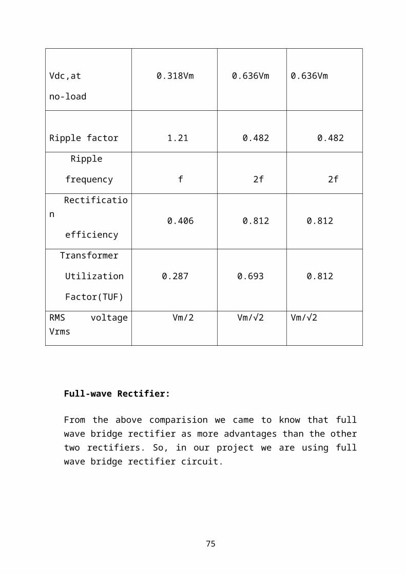
size and shape, but inside it is completely different. First of all, it has an inside – a
normal credit card is a simple piece of plastic. The inside of a smart card usually
contains an Embedded Microprocessor or EEPROM (memory) or some times
both. The microprocessor is under a gold contact pad on one side of the card.
Think of the microprocessor as replacing the usual magnetic stripe on a credit
card or debit card.
BASICS
A smart card is a plastic card with a microprocessor chip embedded
in it. The card looks like a normal credit card except for its metal contact (in
contact card only), but applications performed could be totally different. Other
than normal credit card and bankcard functions, a smart card could act as an
electronic wallet where electronic cash is kept. With the appropriate software, it
could also be used as a secure access control token ranging from door access
control to computer authentication.
The term “smart card” has different meanings in different books
[Guthery1998, Rankl1997] because smart cards have been used in different
applications.
SMART CARD
The smart card is defined as a “Credit Card” with a “Brain” on it, the
brain being a small Embedded Computer Chip. Because of this “Embedded
Brain”, smart card is also known as chip or integrated circuit (IC) card. Some
types of smart card may have a microprocessor embedded, while others may only
have a non-volatile memory content included. In general, a plastic card with a
chip embedded inside can be considered as a smart card.
In either type of smart card, the storage capacity of its memory content is
much larger than that in magnetic stripe cards. The total storage capacity of a
magnetic stripe card is 125 bytes while the typical storage capacity of a smart card
ranges from 1K bytes to 64K bytes. In other words, the memory content of a large
75

capacity smart card can hold the data content of more than 500 magnetic stripe
cards.
Obviously, large storage capacity is one of the advantages in using smart
card, but the single-most important feature of smart card consists of the fact that
their stored data can be protected against unauthorized access and tampering.
Inside a smart card, access to the memory content is controlled by a secure logic
circuit within the chip. As access to data can only is performed via a serial
interface supervised by the operating system and the secure logic system,
confidential data written onto the card is prevented from unauthorized external
access. This secret data can only be processed internally by the microprocessor.
Due to the high security level of smart cards and its off-line nature, it is
extremely difficult to “hack” the value off a card, or otherwise put unauthorized
information on the card. Because it is hard to get the data without authorization,
and because it fits in one’s pocket, a smart card is uniquely appropriate for secure
and convenient data storage. Without permission of the card holder, data could not
be captured or modified. Therefore, smart card could further enhance the data
privacy of user.
Therefore, smart card is not only a data store, but also programmable,
portable, tamper-resistant memory storage.
SMART CARD READER
Smart Card Readers are also known as Card Programmers (because they
can write to a card), card terminals, card acceptance device (CAD) or an interface
device (IFD). When the smart card and the card reader come into contact, each
identifies itself to the other by sending and receiving information. If the messages
exchanged do not match, no further processing takes place.
Smart Card Reader Working
Smart Card Readers are also known as card programmers (because they
can write to a card), card terminals, card acceptance device (CAD) or an interface
76
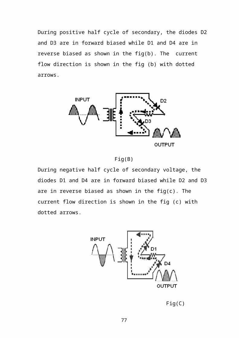
device (IFD). There is a slight difference between the card reader and the
terminal. The term ‘reader’ is generally used to describe a unit that interfaces with
a PC for the majority of its processing requirements. In contrast, a ‘terminal’ is a
self-contained processing device.
The reader provides a path for your application to send and receive
commands from the card. There are many types of readers available, such as
serial, PC Card, and standard keyboard models. Unfortunately, the ISO group was
unable to provide a standard for communicating with the readers so there is no
one-size-fits-all approach to smart card communication.
Each manufacturer provides a different protocol for communication with the
reader.
First you have to communicate with the reader.
Second, the reader communicates with the card, acting as the intermediary
before sending the data to the card.
Third, communication with a smart card is based on the APDU format. The
card will process the data and return it to the reader, which will then return the
data to its originating source.
The following classes are used for communicating with the reader:
ISO command classes for communicating with 7816 protocol
Classes for communicating with the reader
Classes for converting data to a manufacturer-specific format
An application for testing and using the cards for an intended and specific
purpose
Communicating with a Smart Card Reader
The reader provides a path for your application to send and receive commands
from the card. There are many types of readers available, such as serial, PC Card,
and standard keyboard models. Unfortunately, the ISO group was unable to
77

provide a standard for communicating with the readers so there is no one-size-fits-
all approach to smart card communication.
Each manufacturer provides a different protocol for communication with the
reader.
First you have to communicate with the reader.
Second, the reader communicates with the card, acting as the intermediary
before sending the data to the card.
Third, communication with a smart card is based on the APDU format. The
card will process the data and return it to the reader, which will then return
the data to its originating source.
HISTORY
A Card embedded with a microprocessor was first invented by 2
German engineers in 1967. It was not publicized until Roland Moreno, a French
journalist, announced the Smart Card patent in France in 1974 [Rankl1997].
With the advances in microprocessor manufacturing technology, the development
cost of the smart card has been greatly reduced. In 1984, a breakthrough was
achieved when French Postal and Telecommunications services (PTT)
successfully carried out a field trial with telephone cards. Since then, smart cards
are no longer tied to the traditional bankcard market even though the phone card
market is still the largest market of smart cards in 1997.
Due to the establishment of the ISO-7816 specification in 1987 (a worldwide
smart card interface standard), the smart card format is now standardized.
Nowadays, smart cards from different vendors could communicate with the host
machine using a common set of language.
TYPES
According to the definitions of “smart card” in the Smart card technology],
the word smart card has three different meanings:
78
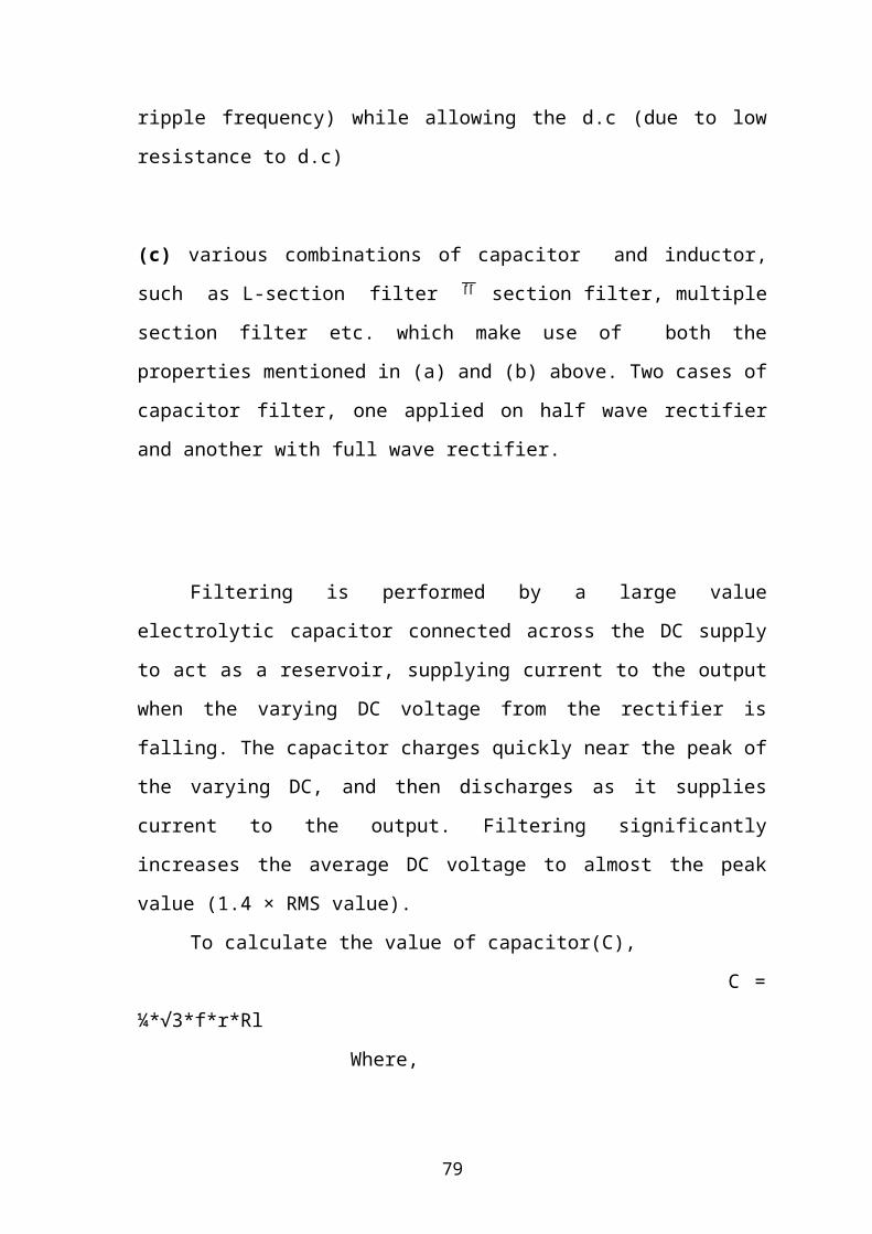
IC card with ISO 7816 interface
Processor IC card
Personal identity token containing Ics
Basically, based on their physical characteristics, IC cards can be
categorized into 4 main types, memory card, contact CPU card, contact-less card
and combi card.
Memory Cards
A memory card is a card with only memory and access logic onboard.
Similar to the magnetic stripe card, a memory card can only be used for
data storage. No data processing capability should be expected. Without
the on-board CPU, memory cards use a synchronous communication
mechanism between the reader and the card where the communication
channel is always under the direct control of the card reader. Data stored
on the card can be retrieved with an appropriate command to the card.
In traditional memory cards, no security control logic is included.
Therefore, unauthorized access to the memory content on the card could not be
prevented. While in current memory cards, with the security control logic
programmed on the card, access to the protection zone is restricted to users with
the proper password only.
Contact CPU Cards
A more sophisticated version of smart card is the contact CPU card. A
microprocessor is embedded in the card. With this real “brain”, program stored
inside the chip can be executed. Inside the same chip, there are four other
functional blocks: the mask-ROM, Non-volatile memory, RAM and I/O port
[HKSAR1997, Rankl1997].
Except for the microprocessor unit, a memory card contains almost all
components that are included in a contact CPU card. Both of them consist of Non-
volatile memory, RAM, ROM and I/O unit. Based on ISO 7816 specifications, the
external appearance of these contact smart cards is exactly the same. The only
79
difference is the existence of the CPU and the use of ROM. In the CPU card,
ROM is masked with the chip’s operating system which executes the commands
issued by the terminal, and returns the corresponding results. Data and application
program codes are stored in the non-volatile memory, usually EEPROM, which
could be modified after the card manufacturing stage.
One of the main features of a CPU card is security. In fact, contact CPU card
has been mainly adopted for secure data transaction. If a user could not
successfully authenticate him/herself to the CPU, data kept on the card could not
be retrieved. Therefore, even when a smart card is lost, the data stored inside the
card will not be exposed if the data is properly stored. Also, as a secure portable
computer, a CPU card can process any internal data securely and outputs the
calculated result to the terminal.
Contact less Cards
Contact less smart card is the one in which the chip communicates with the card
reader through RFID induction technology (at data rates of 106 – 848 Kbits/sec).
These cards require only close proximity to an antenna to complete transaction.
They are often used when transactions must be processed quickly or hands-free,
such as on mass transit systems, where smart cards can be used without even
removing them from a wallet.
Even though contact CPU smart card is more secure than
memory card, it may not be suitable for all kinds of applications, especially where
massive transactions are involved, such as transportation uses. Because in public
transport uses, personal data must be captured by the reader within a short period
of time, contact smart card which requires the user to insert the card to the reader
before the data can be captured from the card would not be a suitable choice.
With the use of radio frequency, the contact-less smart card can transmit user data
from a fairly long distance within a short activation period. The card holder would
not have to insert the card into the reader. The whole transaction process could be
performed without removing the card from the user’s wallet.
80
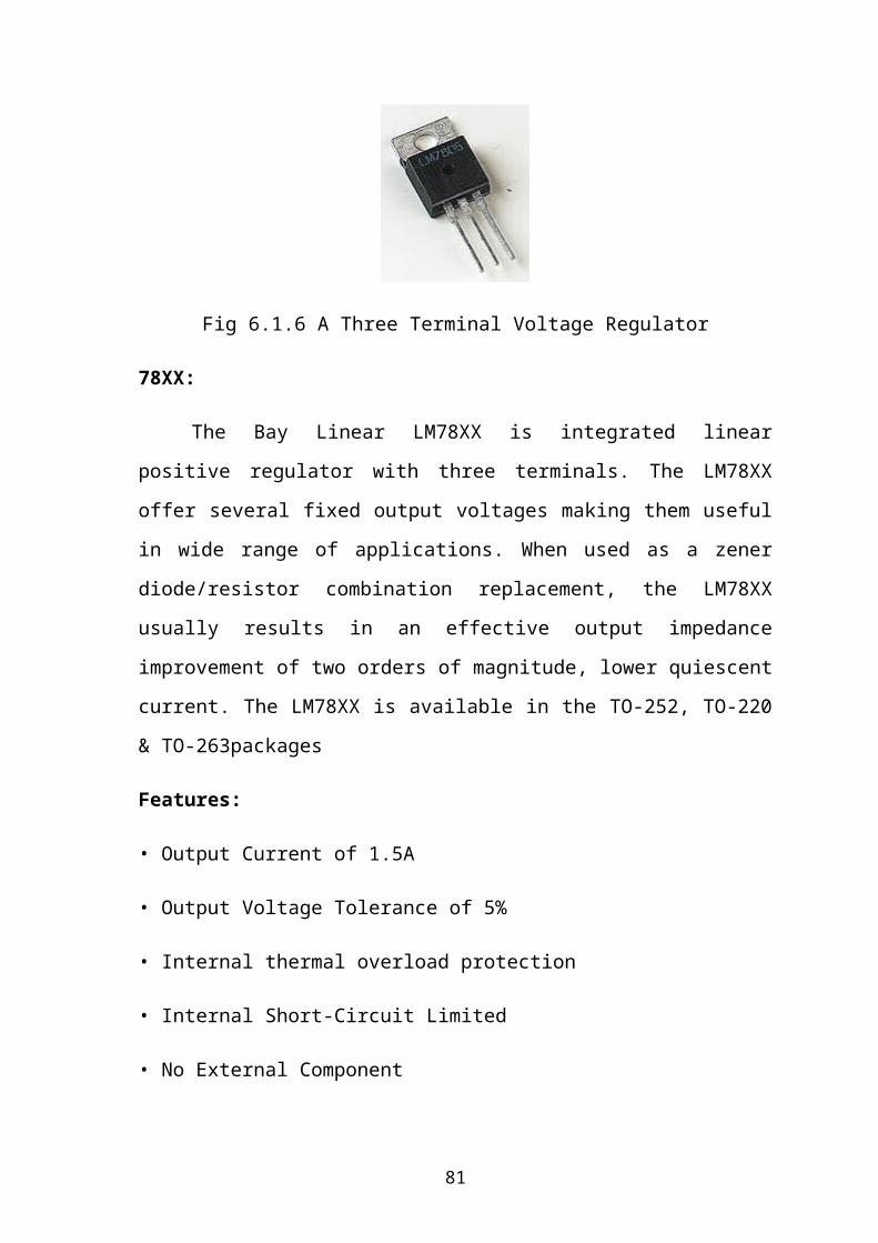
Contact-less smart cards use a technology that enables card readers to provide
power for transactions and communications without making physical contact with
the cards. Usually electromagnetic signal is used for communication between the
card and the reader. The power necessary to run the chip on the card could either
be supplied by the battery embedded in the card or transmitted at microwave
frequencies from the reader onto the card.
Contact-less card is highly suitable for large quantity of card access and data
transaction. However, contact-less smart card has not been standardized. There
are about 16 different contacts-less card technologies and card types in the market
[ADE]. Each of these cards has its specific advantages, but they may not be
compatible with each other. Nevertheless, because of its high production cost and
the technology is relatively new, this type of cards has not been widely adopted.
Combi-Card
At the current stage, contact and contact-less smart card are using two
different communication protocols and development processes. Both cards
have their advantages and disadvantages. Contact smart cards have higher
level of security and readily-available infrastructure, while contact-less
smart card provide a more efficient and convenient transaction
environment. In order to provide customers with the advantages of these
two cards, two methods could be employed. The first method is to build a
hybrid card reader, which could understand the protocols of both types of
cards. The second method is to create a card that combines the contact
functions with the contactless functions. Because the manufacturing cost
of the hybrid reader is very expensive, the later solution is usually chosen.
Sometimes, the term “combi card” is being misused by manufacturers. In
general, there are two types of combine contact-contactless smart cards, namely
the hybrid card and the combi card. Both cards have contact and contactless parts
embedded together in the plastic card. However, in the hybrid card, the contact IC
chip and contactless chip are separate modules. No electrical connections have
been included for communications between the two chips. These two modules can
be considered as separate but co-existing chips on the same card. While in the
81

combi card, the contact and contactless chips could communicate between
themselves, thus giving the combi card the capability to talk with external
environment via either the contact or contactless method.
As the combi cards possess the advantages of both contact and contactless
cards, the only reason that is hindering its acceptance is cost. When the cost and
technical obstacles are overcome, combi cards will become a popular smart card
solution.
In our project the Smart Card used is of the type Contact type cards.
Basically this type of Smart Cards got SIM like Structure Embedded on a Plastic
card for Physical Structure and Strength. There exist different types of SIM
structures according to the type of Application, Memory and features involved in
the Smart Card. Some of them are shown below.
FIG 23 :Types of SIM Structures
These Contact type Smart cards have a contact area, comprising several gold-
plated contact pads, that is about 1cm square. When inserted into a reader, the
chip makes contact with electrical connectors that can read information from the
chip and write information back.
Electrical signals description
82
FIG 24 : Smart Card pin-out
VCC: Power supply input
RST: Either used it (reset signal supplied from the interface device) or in
combination with an internal reset control circuit (optional use by the card). If
internal reset is implemented, the voltage supply on Vcc is mandatory.
CLK: Clocking or timing signal (optional use by the card).
GND: Ground (reference voltage).
VPP: Programming voltage input (deprecated / optional use by the card).
I/O: Input or Output for serial data to the integrated circuit inside the card.
Contact type Smart Card Reader
Contact smart card readers are used as a communications medium between the
smart card and a host, e.g. a computer, a point of sale terminal, or a mobile
telephone.
Since the chips in the financial cards are the same as those used for mobile phone
Subscriber Identity Module (SIM) cards, just programmed differently and
embedded in a different shaped piece of PVC, the chip manufacturers are building
to the more demanding GSM/3G standards. So, for instance, although EMV
allows a chip card to draw 50 mA from its terminal, cards are normally well inside
the telephone industry’s 6mA limit. This is allowing financial card terminals to
become smaller and cheaper.
The reader provides a path for your application to send and receive commands
from the card. There are many types of readers available, such as serial, PC-Card,
83

and standard keyboard models. Unfortunately, the ISO group was unable to
provide a standard for communicating with the readers so there is no one-size-fits-
all approach to smart card communication.
Each manufacturer provides a different protocol for communication with the
reader.
First you have to communicate with the reader.
Second, the reader communicates with the card, acting as the intermediary
before sending the data to the card.
Third, communication with a smart card is based on the APDU format. The
card will process the data and return it to the reader, which will then return the
data to its originating source.
The following classes are used for communicating with the reader:
ISO command classes for communicating with 7816 protocol
Classes for communicating with the reader
Classes for converting data to a manufacturer-specific format
An application for testing and using the cards for an intended and specific
purpose
Readers come in many forms, factors and capabilities. The easiest way to describe
a reader is by the method of its interface to a PC. Smart card readers are available
that interface to RS232 serial ports, USB ports, PCMCIA slots, floppy disk slots,
parallel ports, infrared IRDA ports and keyboards and keyboard wedge readers.
Card readers are used to read data from – and write data to – the smart card.
Readers can easily be integrated into a PC utilizing Windows 98/Me, 2000, or XP
platforms. However, some computer systems already come equipped with a built-
in smart card reader. Some card readers come with advanced security features
such as secure PIN entry, secure display and an integrated fingerprint scanners for
the next-generation of multi-layer security and three-factor authentication.
Another difference in reader types is on-board intelligence and capabilities. An
extensive price and performance difference exists between an industrial strength
reader that supports a wide variety of card protocols and the less expensive win-
84

card reader that only works with microprocessor cards and performs all
processing of the data in the PC.
The options in terminal choices are just as varied. Most units have their own
operating systems and development tools. They typically support other functions
such as magnetic-stripe reading, modem functions and transaction printing.
To process a smart card the computer has to be equipped with a smart card reader
possessing the following mandatory features:
Smart Card Interface Standard – ISO 7816 is an international standard that
describes the interface requirements for contact-type smart cards. These standards
have multiple parts. For instance, part 1, 2 and 3 are applicable to card readers.
Part 1 defines the physical characteristics of the card. Part 2 defines dimension
and location of smart card chip contacts. Part 3 defines the electronic signals and
transmission protocols of the card. Card readers may be referred to as conforming
to ISO 7816 1/2/3, or in its simplified term, ISO 7816.
Driver – This refers to the software used by the operating system (OS) of a
PC for managing a smart card and applicable card reader. To read a smart ID card,
the driver of the card reader must be PC/SC compliant which is supported by most
card reader products currently available. It should be noted that different OS
would require different drivers. In acquiring card readers, the compatibility
between the driver and the OS has to be determined and ensured.
Desirable Features in a Smart Card Reader:
Card Contact Types refers to how the contact between a card reader and a
smart card is physically made. There are two primary types of contact: landing
contact and friction contact (also known as sliding or wiping). For card readers
featuring friction contact, the contact part is fixed. The contact wipes on the card
surface and the chip when a card is inserted. For card readers featuring the landing
type, the contact part is movable. The contact “lands” on the chip after a card is
wholly inserted. In general, card readers of the landing type provide better
protection to the card than that of the friction type.
Smart card readers are also used as smart card programmers to configure
and personalize integrated circuit cards. These programmers not only read data,
85

but also put data into the card memory. This means that not only CPU based smart
cards, but also simple memory cards can be programmed using a smart card
reader. Of course the card reader must support the appropriate protocol such as the
asynchronous T=0, T=1 or synchronous I2C protocols.
The smart card reader here in this project used is the supports the T=0, T=1
protocols. The smart card here used is of 256 bytes of memory (SLE 4442). The
following section gives the some sort of information about the smart card memory
and its interfacing commands.
Features:
256 ´ 8-bit EEPROM organization
Byte-wise addressing
Irreversible byte-wise write protection of lowest 32 addresses (Byte 0 ...
31)
32 ´ 1-bit organization of protection memory
Two-wire link protocol
End of processing indicated at data output
Answer-to-Reset acc. To ISO standard 7816-3
Programming time 2.5 ms per byte for both erasing and writing
Minimum of 104 write/erase cycles1)
86
COMMUNICATION PROTOCOLS
Name Description
T=0 Asynchronous half-duplex byte-level transmission protocol.
T=1 Asynchronous half-duplex block-level transmission protocol.
T=2 Reserved for future full-duplex operations.
T=3 Reserved for future full-duplex operations.
T=CL APDU transmission via contactless interface ISO 14443.
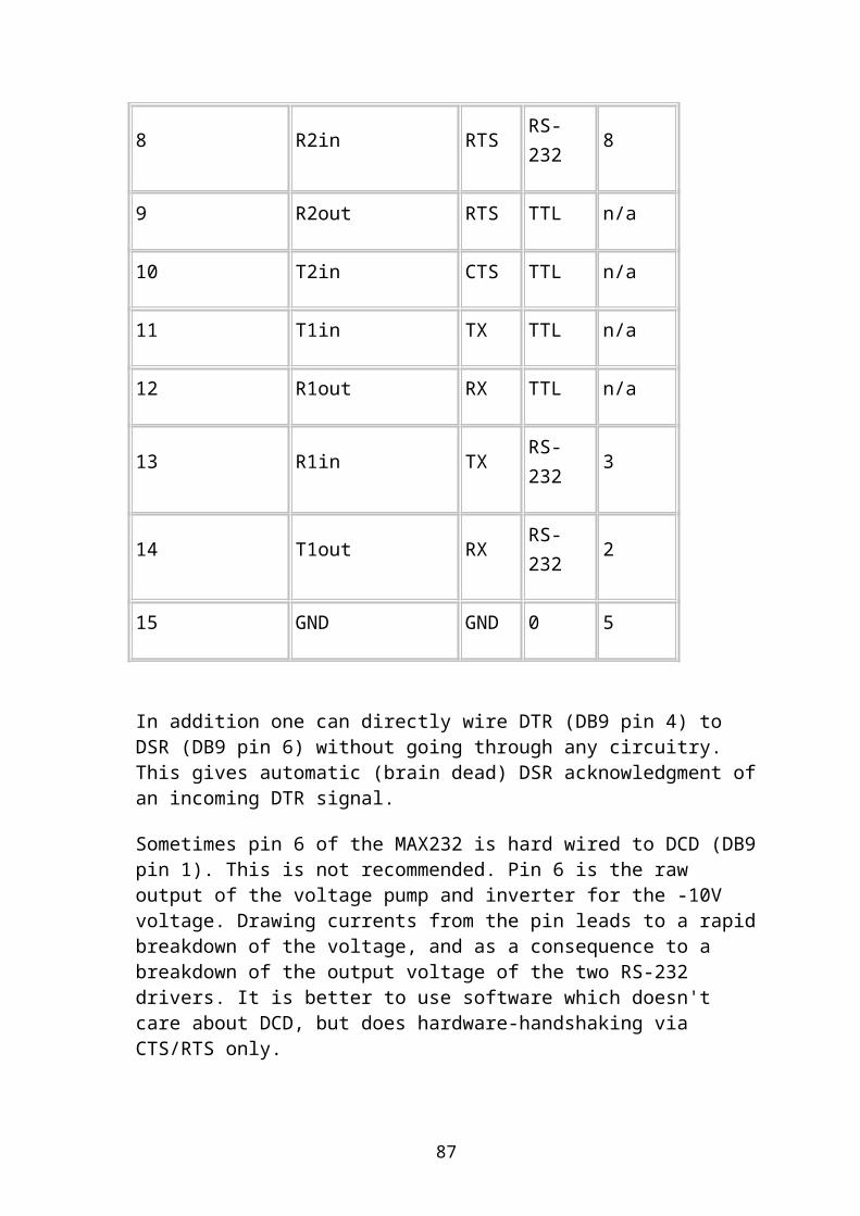
Data retention for minimum of ten years1)
Contact configuration and serial interface in accordance with ISO standard
7816 (synchronous transmission)
Pin configuration:
Pin description:
COMMAND SET FOR SLE4442– 256 bytes Memory
Steps Command Comd to SR90 Prompt from SR90 Reader
1. Set Device Type #0203! #83! (Positive Ack)
#8A! (Invalid Device Type set)
2. Send Card Status #01! #80! (Card Present)
#81! (Card Absent)
87
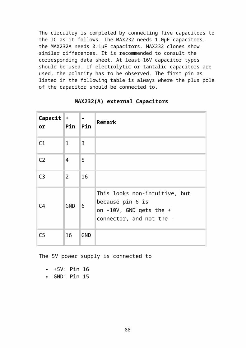
3. ATR #03! #88A2131091!
4. Read Data #10AANN! #87AANNDDD…D!
(DDD = Data)
#86! (Invalid Command)
#82! (No Device Type set)
#8D! (Memory Over Flow)
5. Write Data #11AANNFFFFFF
DD..D! #82! (No Device Type set )
#83! (Positive Ack)
#89! (Invalid Security Code)
#86! (Invalid Command)
#85! (Invalid Parameters
#8D! (Memory over Flow)
#90!(Already Protected)
6. Protect Data #12AANNFFFFFF
DD! #83! (Positive Ack)
#82! (No Device Type)
#89! (Invalid Security Code)
88
#86! (Invalid Command)
#85! (Invalid Parameters
#8D! (Memory Over Flow)
7. Change Security Code #53FFFFFF555555 #83! (Positive Ack)
#89! (Invalid Security Code)
#86! (Invalid Command)
#85! (Invalid Parameters
8. Locations Which can’t write : 0,1,2,3,6,7
9. Communication Protocol: Baud Rate :9,600 bps
Parity :None
Stop Bit :1
Start Bit :0
Data :8 bits
AA = Address location of the chip in Hex
NN = Number of bytes to read or to write
89
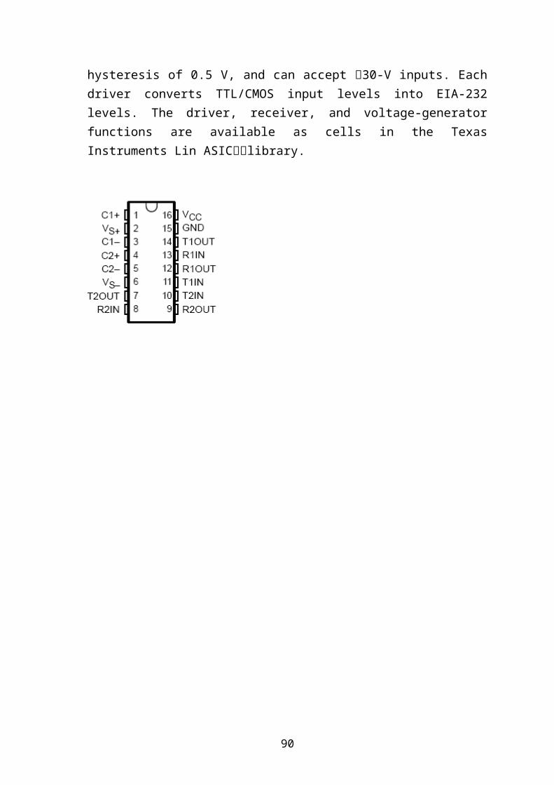
FFFFFF = Security Code
DD = Data to read /write or protect in BCD format
Note: Please give correct security code while writing your cards other wise
they will damage. This card will allow 3 times of writing false security code
later it won’t accept to write the card but you can read.
In our project, the Smart Card Reader communicates with microcontroller
through 2 pins namely RX and TX with the help of a Serial Driver. These 2 pins
are pin 2, 3 of the 9-pin connector of Smart Card Reader.
Fig 25 :SMART CARD READER
APPLICATIONS
With the rapid expansion of Internet technology and
electronic commerce, smart cards are now more widely accepted in the
commercial market as stored-value and secure storage cards. Moreover, it has also
been widely used as an identity card.
The smart card has also been used in transportation such as
the Octopus card which has been adopted by the MTRC and KCRC to replace of
the old Magnetic stripe card. Medical record can also be stored in the smart card.
This enables critical information of the patient to be retrieved whenever it is
90
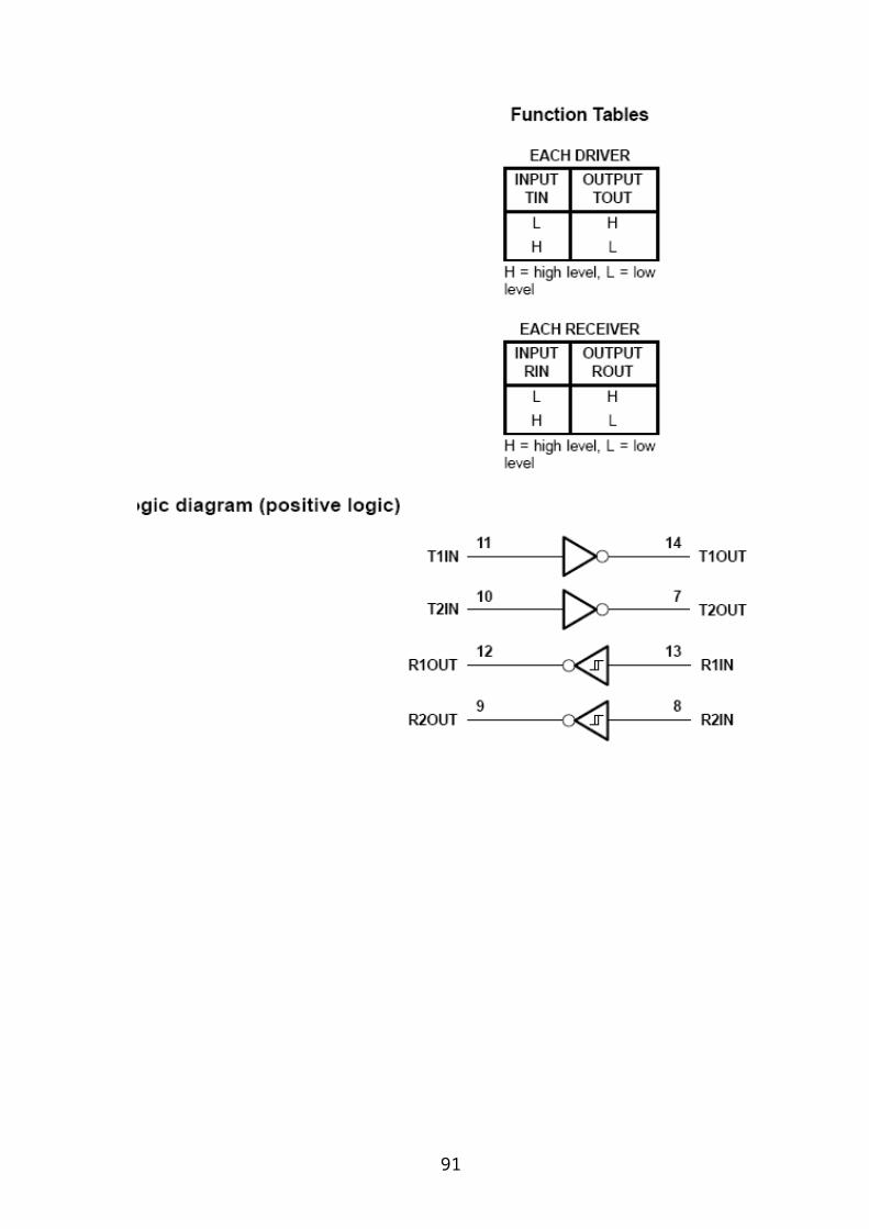
required. With the help of smart card technology, many secure data such as the
computer login name and password can also be kept, so user need not remember a
large number of passwords.
The applications can be classified into 6 main categories: Electronic
Payment, Security and Authentication, Transportation, Telecommunications,
Loyalty Program and Health Care Applications.
1. ELECTRONIC PAYMENT
Electronic Purse
Electronic Purse is also known as electronic cash. Funds can be loaded onto a
card for use as cash. The electronic cash can be used for small purchases without
necessarily requiring the authorization of a PIN. The card is credited from the
cardholder’s bank account or some other ways. When it is used to purchase goods
or services, electronic value is deducted from the card and transferred to the
retailer’s account. Similar to a real wallet, the cardholder could credit his/her card
at the bank any time when required.
Stored Value Cards
Another use of smart cards in electronic commerce is Electronic token. It is an
example of the stored-value card. The principle is that some memory in the smart
card is set aside to store electronic tokens or electronic tickets. A smart card can
store tokens for different services and each of the tokens can be refilled,
depending on the types of the memory card. This allows the cost to be distributed
over a number of services and over a much longer life span.
For example, the card could be used to pay for gas and instead of putting coins in
a parking meter. Consumers load up the card from a vending machine.
2. SECURITY AND AUTHENTICATION
Cryptographic uses
From the point-of-view of the supplier and system operator, the main
requirement of almost all machine-readable card systems is to ensure that the card
91
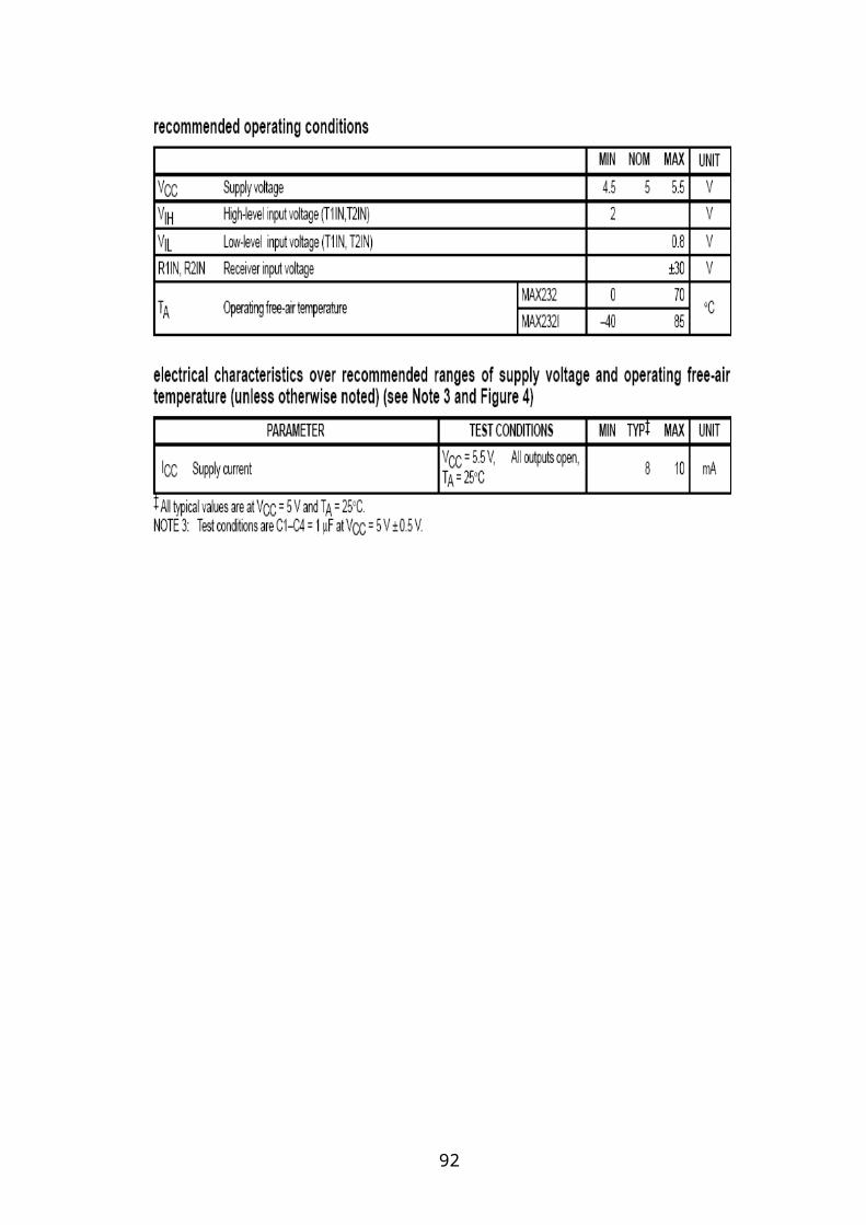
presented is valid and the cardholder is indeed the person entitled to use that
particular card. To verify the cardholder’s identity, users are required to enter their
PIN code (personal identification number). This PIN code is kept in the card
rather than on the terminals or host machines.
Identification and authentication procedures take place at the card terminal.
Identity card
The identification of an individual is one of the most complex processes in
the field of Information Technology. It requires both the individual to identify
himself and for the system to recognize the incoming connection is generated by a
legal user. The system then accepts responsibility for allowing all subsequent
actions, sage in the knowledge that the user has authorization to do whatever he is
asking of the system.
If a smart card is used, the information stored on the card can be verified locally
against a ‘password’ or PIN before connection is made to the host. This prevents
the password from being eavesdropped by perpetrators on the Internet.
Some of the smart cards will have personal data stored on the card. For example,
the cardholder’s name, ID number, and date of birth
Access control card
The most common devices used to control access to private areas where
sensitive work is being carried out or where data is held, are keys, badges and
magnetic cards. These all have the same basic disadvantages: they can easily be
duplicated and when stolen or passed on, they can allow entry by an unauthorized
person. The smart card overcomes these weaknesses by being very difficult to be
reproduced and capable of storing digitized personal characteristics. With suitable
verification equipment, this data can be used at the point of entry to identify
whether the user is the authorized cardholder. The card can also be individually
personalized to allow access to limited facilities, depending on the holder’s
security clearance. A log of the holder’s movements, through a security system,
can be stored on the card as a security audit trail
92

Digital certificate
The most important security measures we encounter in our daily business
have nothing to do with locks and guards. A combination of a signed message and
the use of public key cryptosystem, so called digital signature, are typically used.
A digitally signed message containing a public key is called a certificate. In
addition to a public key, a certificate typically contains a name, address, and other
information describing the holder of the corresponding secret key. All of these
carry the digital signature of a registry service that records public keys for all
members of the community. To become a member of this community, a
subscriber must do two things:
Provide the directory service with a public key and the associated
identification information so that other people will be able to verify his/her
signature.
Obtain the public key of the directory service so that he/she can verify
other people’s signatures.
Because certificates are extremely tamper resistant, the authenticity of a
certificate is a property of the certificate itself, rather than of the authenticity of
the channel over which it was received.
Computer login
Access to the Computer room and its services can be controlled by the
smart card. In terms of network access, smart card can authenticate the user to the
host.
Furthermore, depending on the environment being protected the network access
card can also perform the following functions:
Manipulation of different authentication codes for different levels of
security.
Use of biometric techniques as an added security measure.
Maintaining an audit trail of failures and attempted violations.
93

Meanwhile, in terms of access to the computer room itself, PIN checking can
be done on the card without the need for hard wiring the access points to a central
computer.
The identification of a user is usually done by means of a (Personal Identification
Number) PIN. The PIN is verified by the microcomputer of the card with the PIN
stored in its RAM. If the comparison is negative, the CPU will refuse to work.
The chip also keeps tack of the number of consecutive wrong PIN entries. If this
number reaches a pre-set threshold, the card blocks itself against any further use.
TRANSPORTATION APPLICATIONS
The smart card can act as electronic money for car drivers who would need
to pay a fee before being able to use a road or tunnel. It would then contain a
balance that can be increased at payment stations or in the pre-paid process, and is
decreased for each use.
TELECOMMUNICATION APPLICATIONS
Since 1988, smart card has become an essential component in cellular
phone systems. Network data, subscriber’s information and all mobile network
critical data are kept inside the card. With this card, subscribers could make calls
from any portable telephone. Moreover, through the IC card, any calls through the
mobile phone could be encrypted, and thus ensure privacy. In the future, more and
more value-added services, such as electronic banking, could be supported by
using this microprocessor card.
HEALTH CARE APPLICATIONS
94

Due to the level of security provided for data storage, IC cards offer a new
perspective for healthcare applications. Medical applications of smart cards can be
used for storing information including personal data, insurance policy, emergency
medical information, hospital admission data and recent medical records.
LOYALTY APPLICATIONS
Loyalty program is another important application of smart cards in the
shopping model. The preferred customer status together with detailed information
on shopping habits is stored and processed on the smart card. With this
information, merchants could derive better shopping model or tailor-make
personalized customer shopping profiles. In addition, this shopping habit profile is
kept in the customer’s card; therefore, his/her shopping record could be kept
confidential from unauthorized access.
ENERGY METER
The Energy Meter is a device which takes the 230 V ac input supply and gives out
the same. In other words it just acts as mediator which takes and gives out the
same but it calculates the number of units of energy being consumed. It monitors
the power consumed with respect to time.
In this project this Energy meter is also connected through a Relay to either
switch it ON or OFF according to the balance available in the Smart card being
inserted.
OPTO COUPLERS:
There are many situations where signals and data need to be transferred
from one system to another within a piece of electronics equipment, or from one
piece of equipment to another, without making a direct ëohmicí electrical
connection. Often this is because the source and destination are (or may be at
95
times) at very different voltage levels, like a microprocessor which is operating
from 5V DC but being used to control a triac which is switching 240V AC. In
such situations the link between the two must be an isolated one, to protect the
microprocessor from over voltage damage. Relays can of course provide this kind
of isolation, but even small relays tend to be fairly bulky compared with ICs and
many of todayís other miniature circuit components. Because theyíre electro-
mechanical, relays are also not as reliable ó and only capable of relatively low
speed operation. Where small size, higher speed and greater reliability are
important, a much better alternative is to use an opt coupler. These use a beam of
light to transmit the signals or data across an electrical barrier, and achieve
excellent isolation.
Optocouplers typically come in a small 6-pin or 8-pin IC package, but are
essentially a combination of two distinct devices: an optical transmitter, typically
a gallium arsenide LED (light-emitting diode) and an optical receiver such as a
phototransistor or light-triggered diac. The two are separated by a transparent
barrier which blocks any electrical current flow between the two, but does allow
the passage of light. The basic idea is shown in Fig.1, along with the usual circuit
symbol for an optocoupler. Usually electrical connections to the LED section are
brought out to the pins on one side of the package and those for the
phototransistor or diac to the other side, to physically separate them as much as
possible. This usually allows Optocouplers to withstand voltages of anywhere
96

between 500V and 7500V between input and output. Optocouplers are essentially
digital or switching devices, so they’re best for transferring either on-off control
signals or digital data. Analog signals can be transferred by means of frequency or
pulse-width modulation.
Key Parameters
The most important parameter for most Optocouplers is their transfer
efficiency, usually measured in terms of their current transfer ratio or CTR. This
is simply the ratio between a current change in the output transistor and the
current change in the input LED which produced it. Typical values for CTR range
from 10% to 50% for devices with an output phototransistor and up to 2000% or
so for those with a Darlington transistor pair in the output. Note, however that in
most devices CTR tends to vary with absolute current level. Typically it peaks at a
LED current level of about 10mA, and falls away at both higher and lower current
levels.
RELAYS
Relay is an electrically operated switch. Current flowing through the coil of the
relay creates a magnetic field which attracts a lever and changes the switch
contacts. The coil current can be on or off so relays have two switch positions and
they are double throw (changeover) switches.
97

Relays allow one circuit to switch a second circuit which can be
completely separate from the first. For example a low voltage battery circuit can
use a relay to switch a 230V AC mains circuit. There is no electrical connection
inside the relay between the two circuits; the link is magnetic and mechanical.
The coil of a relay passes a relatively large current, typically 30mA for a
12V relay, but it can be as much as 100mA for relays designed to operate from
lower voltages. Most ICs (chips) cannot provide this current and a transistor is
usually used to amplify the small IC current to the larger value required for the
relay coil. The maximum output current for the popular 555 timer IC is 200mA so
these devices can supply relay coils directly without amplification.
Relays are usually SPDT or DPDT but they can have many more sets of
switch contacts, for example relays with 4 sets of changeover contacts are readily
available. For further information about switch contacts and the terms used to
describe them please see the page on switches.
Most relays are designed for PCB mounting but you can solder wires
directly to the pins providing you take care to avoid melting the plastic case of the
relay. The supplier's catalogue should show you the relay's connections. The coil
will be obvious and it may be connected either way round. Relay coils produce
brief high voltage 'spikes' when they are switched off and this can destroy
98
transistors and ICs in the circuit. To prevent damage you must connect a
protection diode across the relay coil.
The animated picture shows a working relay with its coil and switch
contacts. You can see a lever on the left being attracted by magnetism when the
coil is switched on. This lever moves the switch contacts. There is one set of
contacts (SPDT) in the foreground and another behind them, making the relay
DPDT.
The relay's switch connections are usually labelled COM,
NC and NO:
COM = Common, always connect to this, it is the moving part of the
switch.
NC = Normally Closed, COM is connected to this when the relay coil is
off.
NO = Normally Open, COM is connected to this when the relay coil is on.
Connect to COM and NO if you want the switched circuit to be on when
the relay coil is on.
Connect to COM and NC if you want the switched circuit to be on when
the relay coil is off.
99
Choosing a relay
You need to consider several features when choosing a relay:
1. Physical size and pin arrangement If you are choosing a relay for an
existing PCB you will need to ensure that its dimensions and pin
arrangement are suitable. You should find this information in the supplier's
catalogue.
2. Coil voltage the relay's coil voltage rating and resistance must suit the
circuit powering the relay coil. Many relays have a coil rated for a 12V
supply but 5V and 24V relays are also readily available. Some relays
operate perfectly well with a supply voltage which is a little lower than
their rated value.
3. Coil resistance the circuit must be able to supply the current required by the
relay coil. You can use Ohm's law to calculate the current:
Relay coil current = supply voltage
coil resistance
4. For example: A 12V supply relay with a coil resistance of 400 passes a
current of 30mA. This is OK for a 555 timer IC (maximum output current
200mA), but it is too much for most ICs and they will require a transistor
to amplify the current.
5. Switch ratings (voltage and current) the relay's switch contacts must be
suitable for the circuit they are to control. You will need to check the
voltage and current ratings. Note that the voltage rating is usually higher
for AC, for example: "5A at 24V DC or 125V AC".
6. Switch contact arrangement (SPDT, DPDT etc).
Most relays are SPDT or DPDT which are often described as "single pole
changeover" (SPCO) or "double pole changeover" (DPCO). For further
information please see the page on switches
100
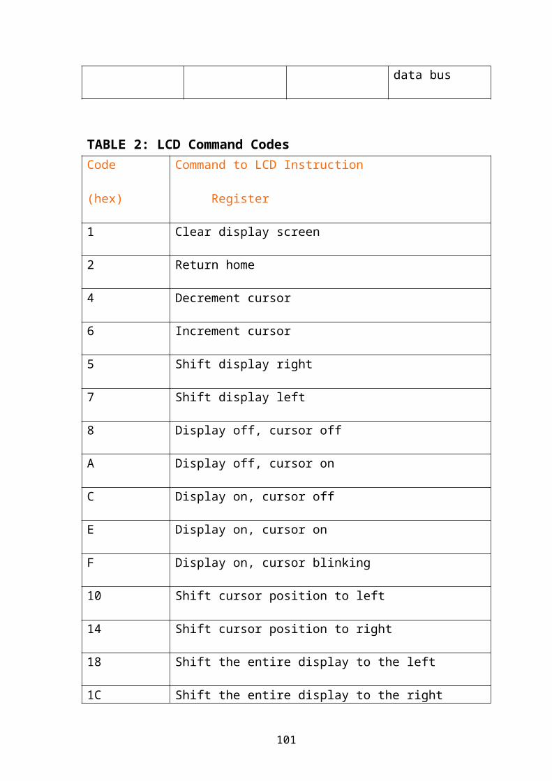
Protection diodes for relays
Transistors and ICs (chips) must be protected from the brief high voltage 'spike'
produced when the relay coil is switched off. The diagram shows how a signal
diode (eg 1N4148) is connected across the relay coil to provide this protection.
Note that the diode is connected 'backwards' so that it will normally not conduct.
Conduction only occurs when the relay coil is switched off, at this moment
current tries to continue flowing through the coil and it is harmlessly diverted
through the diode. Without the diode no current could flow and the coil would
produce a damaging high voltage 'spike' in its attempt to keep the current flowing.
Reed relays
Reed relays consist of a coil surrounding a reed switch.
Reed switches are normally operated with a magnet, but in
a reed relay current flows through the coil to create a magnetic field and close the
reed switch.
Reed relays generally have higher coil resistances than standard relays
(1000 for example) and a wide range of supply voltages (9-20V for example).
They are capable of switching much more rapidly than standard relays, up to
several hundred times per second; but they can only switch low currents (500mA
maximum for example).
Relays and transistors compared
Like relays, transistors can be used as an electrically operated switch. For
switching small DC currents (< 1A) at low voltage they are usually a better choice
101

than a relay. However transistors cannot switch AC or high voltages (such as
mains electricity) and they are not usually a good choice for switching large
currents (> 5A). In these cases a relay will be needed, but note that a low power
transistor may still be needed to switch the current for the relay's coil! The main
advantages and disadvantages of relays are listed below:
Advantages of relays:
Relays can switch AC and DC, transistors can only switch DC.
Relays can switch high voltages, transistors cannot.
Relays are a better choice for switching large currents (> 5A).
Relays can switch many contacts at once.
Disadvantages of relays:
Relays are bulkier than transistors for switching small currents.
Relays cannot switch rapidly (except reed relays), transistors can switch
many times per second.
Relays use more power due to the current flowing through their coil.
Relays require more current than many chips can provide, so a low
power transistor may be needed to switch the current for the relay's coil.
102
SOFTWARE DESCRIPTION
ABOUT SOFTWARE
Software used:*Keil software for c programming
ABOUT KEIL SOFTWARE:
It is possible to create the source files in a text editor such as Notepad, run the Compiler on each C source file, specifying a list of controls, run the Assembler on each Assembler source file, specifying another list of controls, run either the Library Manager or Linker (again specifying a list of controls) and finally running the Object-HEX Converter to convert the Linker output file to an Intel Hex File. Once that has been completed the Hex File can be downloaded to the target hardware and debugged. Alternatively KEIL can be used to create source files; automatically compile, link and covert using options set with an easy to use user interface and finally simulate or perform debugging on the hardware with access to C variables and memory. Unless you have to use the tolls on the command line, the choice is clear. KEIL Greatly simplifies the process of creating and testing an embedded application.
Projects:
The user of KEIL centers on “projects”. A project is a list of all the source files required to build a single application, all the tool options which specify exactly how to build the application, and – if required – how the application should be simulated. A project contains enough information to take a set of source files and generate exactly the binary code required for the application. Because of the high degree of flexibility required from the tools, there are many options that can be set to configure the tools to operate in a specific manner. It would be tedious to have to set these options up every time the application is being built; therefore they are stored in a project file. Loading the project file into KEIL informs KEIL which source files are required, where they are, and how to configure the tools in the correct way. KEIL can then execute each tool with the correct options. It is also possible to create new projects in KEIL. Source files are added to the project and the tool options are set as required. The project can then
103
be saved to preserve the settings. The project is reloaded and the simulator or debugger started, all the desired windows are opened. KEIL project files have the extension
Simulator/Debugger:
The simulator/ debugger in KEIL can perform a very detailed simulation of a micro controller along with external signals. It is possible to view the precise execution time of a single assembly instruction, or a single line of C code, all the way up to the entire application, simply by entering the crystal frequency. A window can be opened for each peripheral on the device, showing the state of the peripheral. This enables quick trouble shooting of mis-configured peripherals. Breakpoints may be set on either assembly instructions or lines of C code, and execution may be stepped through one instruction or C line at a time. The contents of all the memory areas may be viewed along with ability to find specific variables. In addition the registers may be viewed allowing a detailed view of what the microcontroller is doing at any point in time.
The Keil Software 8051 development tools listed below are the programs you use to compile your C code, assemble your assembler source files, link your program together, create HEX files, and debug your target program. µVision2 for Windows™ Integrated Development Environment: combines Project Management, Source Code Editing, and Program Debugging in one powerful environment.
C51 ANSI Optimizing C Cross Compiler: creates relocatable object modules from your C source code,
A51 Macro Assembler: creates relocatable object modules from your 8051 assembler source code,
BL51 Linker/Locator: combines relocatable object modules created by the compiler and assembler into the final absolute object module,
LIB51 Library Manager: combines object modules into a library, which may be used by the linker,
OH51 Object-HEX Converter: creates Intel HEX files from absolute object modules.
What's New in µVision3?µVision3 adds many new features to the Editor like Text Templates, Quick Function Navigation, and Syntax Coloring with brace high lighting Configuration Wizard for dialog based startup and debugger setup. µVision3 is fully compatible to µVision2 and can be used in parallel with µVision2.
104
What is µVision3?µVision3 is an IDE (Integrated Development Environment) that helps you write, compile, and debug embedded programs. It encapsulates the following components:
A project manager. A make facility. Tool configuration. Editor. A powerful debugger.
To help you get started, several example programs (located in the \C51\Examples, \C251\Examples, \C166\Examples, and \ARM\...\Examples) are provided.
HELLO is a simple program that prints the string "Hello World" using the Serial Interface.
MEASURE is a data acquisition system for analog and digital systems. TRAFFIC is a traffic light controller with the RTX Tiny operating system. SIEVE is the SIEVE Benchmark. DHRY is the Dhrystone Benchmark. WHETS is the Single-Precision Whetstone Benchmark.
Additional example programs not listed here are provided for each device architecture.
Building an Application in µVision2To build (compile, assemble, and link) an application in µVision2, you must:
1. Select Project -(forexample,166\EXAMPLES\HELLO\HELLO.UV2).2. Select Project - Rebuild all target files or Build target.
µVision2 compiles, assembles, and links the files in your project
Creating Your Own Application in µVision2 To create a new project in µVision2, you must:
1. Select Project - New Project.2. Select a directory and enter the name of the project file.3. Select Project - Select Device and select an 8051, 251, or C16x/ST10
device from the Device Database™.4. Create source files to add to the project.5. Select Project - Targets, Groups, Files. Add/Files, select Source Group1,
and add the source files to the project.6. Select Project - Options and set the tool options. Note when you select the
target device from the Device Database™ all special options are set automatically. You typically only need to configure the memory map of your target hardware. Default memory model settings are optimal for most applications.
105

7. Select Project - Rebuild all target files or Build target.Debugging an Application in µVision2To debug an application created using µVision2, you must:
1. Select Debug - Start/Stop Debug Session.2. Use the Step toolbar buttons to single-step through your program. You may
enter G, main in the Output Window to execute to the main C function.3. Open the Serial Window using the Serial #1 button on the toolbar.
Debug your program using standard options like Step, Go, Break, and so on.
Starting µVision2 and Creating a Project
µVision2 is a standard Windows application and started by clicking on the program icon. To create a new project file select from the µVision2 menu
Project – New Project…. This opens a standard Windows dialog that asks you
for the new project file name.
We suggest that you use a separate folder for each project. You can simply use
the icon Create New Folder in this dialog to get a new empty folder. Then
select this folder and enter the file name for the new project, i.e. Project1.
µVision2 creates a new project file with the name PROJECT1.UV2 which contains
a default target and file group name. You can see these names in the Project
Window – Files.
Now use from the menu Project – Select Device for Target and select a CPU
for your project. The Select Device dialog box shows the µVision2 device
database. Just select the micro controller you use. We are using for our examples the Philips 80C51RD+ CPU. This selection sets necessary tool
options for the 80C51RD+ device and simplifies in this way the tool Configuration
Building Projects and Creating a HEX Files
Typical, the tool settings under Options – Target are all you need to start a new
application. You may translate all source files and line the application with a
106
click on the Build Target toolbar icon. When you build an application with
syntax errors, µVision2 will display errors and warning messages in the Output
Window – Build page. A double click on a message line opens the source file
on the correct location in a µVision2 editor window.
Once you have successfully generated your application you can start debugging.
After you have tested your application, it is required to create an Intel HEX file to download the software into an EPROM programmer or simulator. µVision2 creates HEX files with each build process when Create HEX files under Options for Target – Output is enabled. You may start your PROM programming utility after the make process when you specify the program under the option Run User Program #1.
CPU Simulation:
µVision2 simulates up to 16 Mbytes of memory from which areas can be
mapped for read, write, or code execution access. The µVision2 simulator traps
and reports illegal memory accesses.
In addition to memory mapping, the simulator also provides support for the
Integrated peripherals of the various 8051 derivatives. The on-chip peripherals
of the CPU you have selected are configured from the Device.
Database selection:
you have made when you create your project target. Refer to page 58 for more
Information about selecting a device. You may select and display the on-chip peripheral components using the Debug menu. You can also change the aspects of each peripheral using the controls in the dialog boxes.
Start Debugging:
You start the debug mode of µVision2 with the Debug – Start/Stop Debug
Session command. Depending on the Options for Target – Debug
Configuration, µVision2 will load the application program and run the startup
107

code µVision2 saves the editor screen layout and restores the screen layout of the last debug session. If the program execution stops, µVision2 opens an
editor window with the source text or shows CPU instructions in the disassembly window. The next executable statement is marked with a yellow arrow. During debugging, most editor features are still available.
For example, you can use the find command or correct program errors. Program source text of your application is shown in the same windows. The µVision2 debug mode differs from the edit mode in the following aspects:
_ The “Debug Menu and Debug Commands” described on page 28 are
Available. The additional debug windows are discussed in the following.
_ The project structure or tool parameters cannot be modified. All build
Commands are disabled.
Disassembly Window
The Disassembly window shows your target program as mixed source and assembly program or just assembly code. A trace history of previously executed instructions may be displayed with Debug – View Trace Records. To enable the trace history, set Debug – Enable/Disable Trace Recording.
If you select the Disassembly Window as the active window all program step commands work on CPU instruction level rather than program source lines. You can select a text line and set or modify code breakpoints using toolbar buttons or the context menu commands.
You may use the dialog Debug – Inline Assembly… to modify the CPU instructions. That allows you to correct mistakes or to make temporary changes to the target program you are debugging.
SOFTWARE COMPONENTS
About Keil
1. Click on the Keil u Vision Icon on Desktop
2. The following fig will appear
108
3. Click on the Project menu from the title bar
4. Then Click on New Project
5. Save the Project by typing suitable project name with no extension in u r own folder sited in either C:\ or D:\
109

6. Then Click on Save button above.
7. Select the component for u r project. i.e. Atmel……
8. Click on the + Symbol beside of Atmel
110

9. Select AT89C51 as shown below
10. Then Click on “OK”
11. The Following fig will appear
111
12. Then Click either YES or NO………mostly “NO”
13. Now your project is ready to USE
14. Now double click on the Target1, you would get another option
“Source group 1” as shown in next page.
15. Click on the file option from menu bar and select “new”
112
16. The next screen will be as shown in next page, and just maximize it by
double clicking on its blue boarder.
17. Now start writing program in either in “C” or “ASM”
18. For a program written in Assembly, then save it with extension “. asm”
and for “C” based program save it with extension “ .C”
113
19. Now right click on Source group 1 and click on “Add files to Group Source”
20. Now you will get another window, on which by default “C” files will appear.
114

21. Now select as per your file extension given while saving the file
22. Click only one time on option “ADD”
23. Now Press function key F7 to compile. Any error will appear if so
happen.
24. If the file contains no error, then press Control+F5 simultaneously.
115

25. The new window is as follows
26. Then Click “OK”
27. Now Click on the Peripherals from menu bar, and check your required
port as shown in fig below
28. Drag the port a side and click in the program file.
116
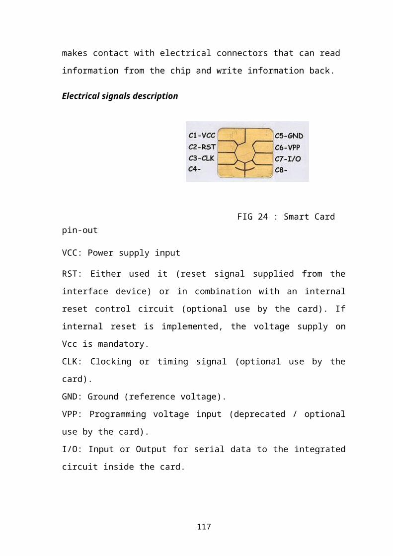
29. Now keep Pressing function key “F11” slowly and observe.
30. You are running your program successfully
Embedded C:
What is an embedded system?
An embedded system is an application that contains at least one
programmable computer and which is used by individuals who are, in the main,
unaware that the system is computer-based.
Which programming language should you use?
Having decided to use an 8051 processor as the basis of your embedded
system, the next key decision that needs to be made is the choice of programming
language. In order to identify a suitable language for embedded systems, we might
begin by making the following observations:
117
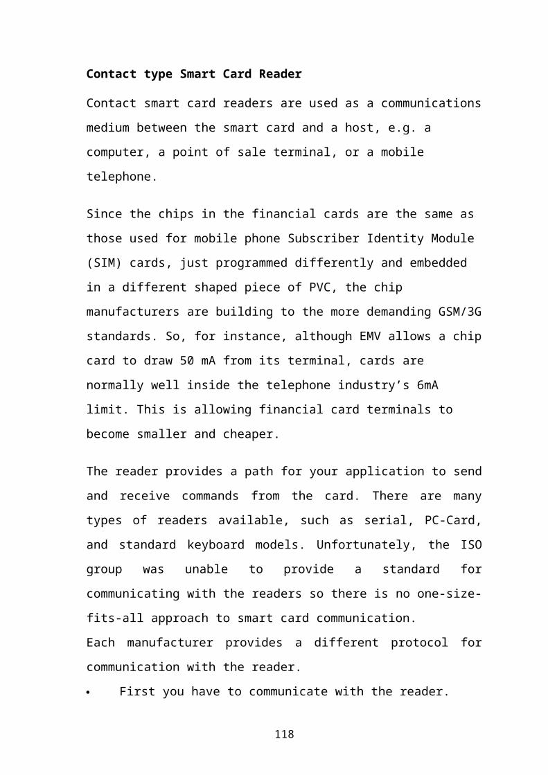
Computers (such as microcontroller, microprocessor or DSP chips) only
accept instructions in ‘machine code’ (‘object codes’). Machine code is, by
definition, in the language of the computer, rather than that of the
programmer. Interpretation of the code by the programmer is difficult and
error prone.
All software, whether in assembly, C, C++, Java or Ada must ultimately be
translated into machine code in order to be executed by the computer.
Embedded processors – like the 8051 – have limited processor power and
very limited memory available: the language used must be efficient.
The language chosen should be in common use.
Summary of C language Features:
It is ‘mid-level’, with ‘high-level’ features (such as support for functions and
modules), and ‘low-level’ features (such as good access to hardware via pointers).
It is very efficient.
It is popular and well understood.
Even desktop developers who have used only Java or C++ can soon
understand C syntax.
Good, well-proven compilers are available for every embedded processor
(8-bit to 32-bit or more).
Basic C program structure:
//- - - - - - - - - - - - - - - - - - - - - - - - - - - - - - - - - - - - -
//Basic blank C program that does nothing
// Includes
118
//- - - - - - - - - - - - - - - - - - - - - - - - - - - - - - - - - - - - -
#include <reg51.h> // SFR declarations
Void main (void)
{
While (1);
{
Body of the loop // Infinite loop
}
} // match the braces
ADVANTAGES:
Reduce the cost of theft and corruption on the electricity distribution
network with electronic designs and prepayment interfaces. Prepayment
meters ensure energy meters now exist that measure current in both phase
and neutral and calculate power consumption based on the larger of the two
currents. As discussed below, these solutions no longer have to be
populated with many components on a printed circuit board. Highly
integrated solutions exist to reduce cost and improve reliability.
Improve the cost and quality of electricity distribution through remote
meter reading and efficient data management. Besides reducing the cost of
manually reading meters, power outages can be detected, identified, and
corrected more quickly for customers whose meters are communicating
through a network.
119

Environmental pollution is minimized by reducing the size of power
generation equipment. Peak usage is minimized despite population growth
through multiple rate billing and distribution cleanliness is maintained by
monitoring power quality pollution contributed by individual consumers.
LIMITATIONS:
Increased security risks from network or remote access
Greater potential for monitoring by other/unauthorized third parties.
The Centralized administration system in control station still needs
future development.
APPLICATIONS:
1. Home applications.2. Industrial applications.3. Power distributions.4. Laboratories.5. Consumer applications.
CONCLUSION:
The project “IMPLEMENTATION OF SMART SYSTEM BASED ON
SMART GRID SMART METER AND SMART APPLIANCES” has been
successfully designed and tested. Integrating features of all the hardware
components used have developed it. Presence of every module has been reasoned
out and placed carefully thus contributing to the best working of the unit.
Secondly, using highly advanced IC’s and with the help of growing technology
the project has been successfully implemented.
120

FUTURE ASPECTS:
Most of the smart card systems in use today serve one purpose and are
related to just one process or is hardwired to only one application. A smart card
cannot justify its existence in this respect. The approach of future smart card is
therefore towards designing multi-application card with own operating system
based on open standard that can perform a variety of functions. It must be
configurable and programmable and it must be able to adapt to new situations and
new requirements especially in areas such as security, memory management, and
operating system. Most of smart card application methods today rely on the fact
that the code of functions to be performed should be imported by card operating
system from an outside server.
In the future, smart cards could handle multiple tasks for their owners, from
providing access to company networks, enabling electronic commerce, storing
health care information, providing ticket-less airline travel and car rentals, and
offering electronic identification for accessing government services such as
benefit payments and drivers licenses etc. Smart cards of the future may even stop
resembling "cards" as smart card technology is embedded into rings, watches,
badges, and other forms and factors that will make them remarkably convenient to
use. In the near future, we believe all PC’s and Network Computers will be
integrated with smart card readers.
REFERENCES:
[1] The 8051 Micro controller and Embedded Systems by -Muhammad Ali
Mazidi, Janice Gillispie Mazidi
[2] Electronic Components -D.V.Prasad
[3] Wireless Communications - Theodore S. Rappaport
[4] Power systems by C.L. Wadhwa
[5] Electrical Machines by J.B. Gupta
121

[6] Syed Khizar Ali Zaidi, Hura Masroor , Syed Rehan Ashrafand Ahmed
Hassan , “Design and implementation of Low cost Electronic Prepaid energy
meter” Proceedings of the 12th IEEE International Multi topic Conference, pp.
542–552, , December 23-24,2008.
[7] N.LOCI, F.MOSSI AND M.TOSI “Virtual Instrument For Instantaneous
Power Measurement”,IEEE TRANS INSTRUM MEAS, VOL 41,NO 4,PP 528-
534 Aug 2002.
[8] The-8051:Micro-Controller, Architecture,Programming & Applications (2nd
edition) by KENNETH J. AYALA,Penaram International Pvt Ltd
[9] Paul Daigle “The Latest On Electronic Meters” Product Manager, Analog
Devices, Inc, masseachusetts.
[10] Rachel Kaplan, energy measurement ic’s simplify meter design –.
[11] Rajkamal, embedded systems architecture programming and design, 2nd
edition. tata mcgraw hill, 2008.
122