gsm siemens tc35 datasheet - · pdf filecopyright ' siemens ag 2001 trademark notice ......
TRANSCRIPT

TC35TC37Siemens Cellular Engines
HardwareInterface
Description
Version: 03.10DocID: TC35_37_HD_02_V03.10

TC35 / TC37 Hardware Interface Description
TC35_37_HD_02_V03.10 - Released Page 2 of 92 21.12.2001
Document Name: TC35 / TC37 Hardware Interface DescriptionVersion: 03.10Date: 21.12.2001
Technical Support: [email protected]
DocId: TC35_37_HD_02_V03.10Status: Released
General notesWith respect to any damages arising in connection with the described product or this document,Siemens shall be liable according to the General Conditions on which the delivery of the describedproduct and this document are based.This product is not intended for use in life support appliances, devices or systems where a malfunctionof the product can reasonably be expected to result in personal injury. Siemens AG customers using orselling this product for use in such applications do so at their own risk and agree to fully indemnifySiemens for any damages resulting from illegal use or resale.Applications incorporating the described product must be designed to be in accordance with thetechnical specifications provided in these guidelines. Failure to comply with any of the requiredprocedures can result in malfunctions or serious discrepancies in results.Furthermore, all safety instructions regarding the use of mobile technical systems, including GSMproducts, which also apply to cellular phones must be followed.Handheld applications such as mobile phones or PDAs incorporating the described product must be inaccordance with the guidelines for human exposure to radio frequency energy. The Specific AbsorptionRate (SAR) of the application must be evaluated and approved to be compliant with national andinternational safety standards or directives.
Subject to change without notice at any time.
Copyright noticeCopying of this document and giving it to others and the use or communication of the contents thereof,are forbidden without express authority. Offenders are liable to the payment of damages. All rightsreserved in the event of grant of a patent or the registration of a utility model or design.
Copyright © Siemens AG 2001
Trademark noticeMS Windows is a registered trademark of Microsoft Corporation.

TC35 / TC37 Hardware Interface Description
TC35_37_HD_02_V03.10 - Released Page 3 of 92 21.12.2001
Contents
0 Version History........................................................................................................... 7
1 Introduction ................................................................................................................ 81.1 Scope of the document and related documents .................................................. 81.2 Terms and abbreviations ..................................................................................... 91.3 Standards.......................................................................................................... 121.4 Safety Precautions ............................................................................................ 13
2 Functions overview .................................................................................................. 152.1 TC35 / TC37 key features at a glance............................................................... 162.2 Block diagram of TC35...................................................................................... 182.3 Block diagram of TC37...................................................................................... 192.4 GSM baseband processor................................................................................. 20
2.4.1 Features of the GSM baseband processor .......................................... 20
3 Application Interface ................................................................................................ 213.1 Operating modes............................................................................................... 223.2 Power supply..................................................................................................... 23
3.2.1 Minimizing power losses ...................................................................... 243.2.2 Battery pack......................................................................................... 253.2.2.1 Recommended battery pack ................................................................ 263.2.2.2 Supported charging technique ............................................................. 273.2.2.3 Operating modes during charging........................................................ 283.2.2.4 Charger requirements.......................................................................... 29
3.3 Power up / down scenarios................................................................................ 303.3.1 Turn on the GSM engine...................................................................... 303.3.1.1 Turn on GSM engine using the ignition line IGT (Power on) ................ 303.3.1.2 Timing of the ignition process .............................................................. 313.3.1.3 Turn on GSM engine using the POWER lines ..................................... 323.3.1.4 Turn on GSM engine using the RTC (Alarm mode) ............................. 323.3.2 Power saving ....................................................................................... 333.3.3 Wake up GSM engine.......................................................................... 333.3.4 Turn off GSM engine ........................................................................... 343.3.4.1 Turn off GSM engine using AT command............................................ 343.3.4.2 Emergency shutdown using /PD pin .................................................... 343.3.4.3 Automatic shutdown ............................................................................ 353.3.5 Summary of state transitions ............................................................... 37
3.4 RTC backup ...................................................................................................... 383.5 Serial interface .................................................................................................. 403.6 Audio interface .................................................................................................. 42
3.6.1 Speech processing .............................................................................. 433.7 SIM interface ..................................................................................................... 44
3.7.1 Approval considerations....................................................................... 443.7.2 Design considerations for SIM card holder .......................................... 453.7.3 Grounding the SIM interface ................................................................ 46
3.8 Control signals................................................................................................... 473.8.1 Inputs................................................................................................... 473.8.2 Outputs................................................................................................ 483.8.2.1 Synchronization signal ......................................................................... 483.8.2.2 Using the SYNC pin to control a status LED........................................ 49

TC35 / TC37 Hardware Interface Description
TC35_37_HD_02_V03.10 - Released Page 4 of 92 21.12.2001
3.8.2.3 Behaviour of the RING0 line ................................................................ 503.9 Pin assignment.................................................................................................. 51
4 Radio interface ......................................................................................................... 564.1 Receiver ............................................................................................................ 564.2 Transmitter ........................................................................................................ 564.3 Antenna interface (antenna reference point ARP) .......................................... 57
4.3.1 Options of connecting the antenna ...................................................... 574.3.2 Description of antenna ports and connectors....................................... 58
5 Physical characteristics........................................................................................... 595.1 Exploded diagram and PCBs............................................................................. 595.2 Mechanical dimensions of TC35 and TC37 ....................................................... 605.3 Mounting TC35/TC37 onto the application platform........................................... 63
5.3.1 Mounting TC35 .................................................................................... 635.3.2 Mounting TC37 .................................................................................... 645.3.3 Positioning labels on TC35 and TC37.................................................. 65
5.4 ZIF connector .................................................................................................... 675.4.1 Mechanical dimensions of the ZIF connector ....................................... 68
5.5 Antenna design ................................................................................................. 695.5.1 GSC antenna connector on TC35........................................................ 695.5.2 Using antenna eqipment from other manufacturers ............................. 725.5.3 Antenna pad and coaxicon connector on TC37 ................................... 73
6 Electrical, temperature and radio characteristics.................................................. 746.1 Absolute maximum ratings ................................................................................ 746.2 Operating conditions ......................................................................................... 746.3 Temperature conditions..................................................................................... 746.4 Power supply ratings ......................................................................................... 75
6.4.1 Drop definition ..................................................................................... 756.4.2 Current consumption during transmit burst .......................................... 76
6.5 Electrical characteristics of the voiceband part .................................................. 806.5.1 Setting audio parameters by AT commands ........................................ 806.5.2 Characteristics of audio modes............................................................ 816.5.3 Voiceband receive path ....................................................................... 826.5.4 Voiceband transmit path ...................................................................... 83
6.6 Air interface ....................................................................................................... 846.7 Electrostatic discharge ...................................................................................... 85
7 Updating Firmware................................................................................................... 86
8 Reference Approval.................................................................................................. 878.1 Reference Equipment........................................................................................ 878.2 CE Conformity................................................................................................... 888.3 G.C.F. Conformity ............................................................................................. 88
9 APPENDIX: List of parts and accessories .............................................................. 899.1 Specifications of AMP switching connector ....................................................... 90
TC35 / TC37 Hardware Interface Description
TC35_37_HD_02_V03.10 - Released Page 5 of 92 21.12.2001
Figures
Figure 1: Block diagram of TC35 ......................................................................................... 18Figure 2: Block diagram of TC37 ......................................................................................... 19Figure 3: Block diagram of a cellular application.................................................................. 21Figure 4: Power supply limits during transmit burst.............................................................. 24Figure 5: Battery pack circuit diagram ................................................................................. 25Figure 6: Charging process ................................................................................................. 27Figure 7: Power-on by ignition signal ................................................................................... 30Figure 8: Timing of power-on process if VDDLP is not used................................................ 31Figure 9: Timing of power-on process if VDDLP is fed from external source ....................... 31Figure 10: Deactivating GSM engine by Power Down signal ............................................... 34Figure 11: RTC supply from capacitor ................................................................................. 38Figure 12: RTC supply from rechargeable battery (accumulator) ........................................ 38Figure 13: RTC supply from non-chargeable battery ........................................................... 39Figure 14: RS-232 interface................................................................................................. 40Figure 15: Audio block diagram ........................................................................................... 42Figure 16: SIM card holder of DSB35 Support Box.............................................................. 45Figure 17: Connecting a separate ground for SIM interface ................................................ 46Figure 18: TC35 output control signals ................................................................................ 48Figure 19: LED Circuit (Example) ........................................................................................ 49Figure 20: Incoming voice call ............................................................................................. 50Figure 21: Incoming data call............................................................................................... 50Figure 22: Antenna connector circuit on TC35..................................................................... 57Figure 23: Antenna connector circuit on TC37..................................................................... 57Figure 24: Exploded diagram and PCBs of TC35/TC37 ...................................................... 59Figure 25: TC35 / TC37 view of RF part ........................................................................... 60Figure 26: Mechanical dimensions of TC35......................................................................... 61Figure 27: Mechanical dimensions of TC37......................................................................... 62Figure 28: Mounting TC35 (example) .................................................................................. 63Figure 29: Mounting TC37 (example) .................................................................................. 64Figure 30: Positioning labels................................................................................................ 65Figure 31: Label dimensions................................................................................................ 65Figure 32: Content of TC35 label......................................................................................... 66Figure 33: Mechanical dimensions of ZIF connector............................................................ 68Figure 34: PCB ZIF connector ............................................................................................. 68Figure 35: Mechanical dimensions of MuRata GSC connector (in mm) ............................... 70Figure 36: Maximum mechanical stress to the connector .................................................... 71Figure 37: How to use MuRata tool ..................................................................................... 71Figure 38: Dimensions and position of coaxicon connector and antenna pad on TC37 ....... 73Figure 39: Typical current (peak) vs power control level ...................................................... 76Figure 40: Typical current (average) vs power control level ................................................. 76Figure 41: Typical current consumption for GSM 900, power level = 5 ................................ 78Figure 42: Typical current consumption for DCS1800, power level = 0................................ 78Figure 43: AT audio programming model ............................................................................ 80Figure 44: Structure of audio inputs..................................................................................... 83Figure 45: Reference equipment for approval...................................................................... 87

TC35 / TC37 Hardware Interface Description
TC35_37_HD_02_V03.10 - Released Page 6 of 92 21.12.2001
Tables
Table 1: TC35 / TC37 key features...................................................................................... 16Table 2: Overview of operating modes ................................................................................ 22Table 3: Power supply pins of ZIF connector....................................................................... 23Table 4: Specifications of CGP34506 Panasonic battery pack ............................................ 26Table 5: AT commands available in Charge-only mode....................................................... 29Table 6: AT commands available in Alarm mode................................................................. 32Table 7: Wake-up events..................................................................................................... 33Table 8: Temperature dependent behaviour........................................................................ 35Table 9: Dependency on ambient temperature.................................................................... 36Table 10: State transitions of TC35 / TC37.......................................................................... 37Table 11: DCE-DTE wiring .................................................................................................. 40Table 12: Signal of the SIM interface (ZIF connector).......................................................... 44Table 13 : Pin assignment of Molex SIM card holder on DSB35 Support Box ..................... 45Table 14: Input control signals of the TC35/TC37 module ................................................... 47Table 15: TC35 synchronization signal (if SYNC pin is set to mode 0 via AT^SSYNC)........ 48Table 16: Modes of the LED and associated functions ........................................................ 49Table 17: Ring signal........................................................................................................... 50Table 18: Pin assignment .................................................................................................... 51Table 19: Return loss .......................................................................................................... 57Table 20: Signals available on GSC jack ............................................................................. 58Table 21: Signals available on antenna pad / coaxicon connector ....................................... 58Table 22: Electrical and mechanical characteristics of the ZIF connector ............................ 67Table 23: Ratings and characteristics of the GSC antenna connector ................................. 69Table 24: Stress characteristics of the GSC antenna connector.......................................... 71Table 25: Ordering information for antenna equipment from AMP Tyco Electronics............ 73Table 26: Absolute maximum ratings................................................................................... 74Table 27: Operating conditions............................................................................................ 74Table 28: Temperature conditions ....................................................................................... 74Table 29: Power supply ratings............................................................................................ 75Table 30: Power control levels GSM 900, power class 4 ..................................................... 77Table 31: Power control levels DCS 1800, power class 1 .................................................... 77Table 32: GSM 900, power level 5....................................................................................... 79Table 33: GSM 1800, power level 0..................................................................................... 79Table 34: Audio parameters adjustable by AT command..................................................... 80Table 35: Voiceband characteristics (typical), all values preliminary.................................... 81Table 36: Voiceband receive path ....................................................................................... 82Table 37: Voiceband transmit path ...................................................................................... 83Table 38: Air Interface ......................................................................................................... 84Table 39: Measured electrostatic values.............................................................................. 85Table 40: List of accessories ............................................................................................... 89

TC35 / TC37 Hardware Interface Description
TC35_37_HD_02_V03.10 - Released Page 7 of 92 21.12.2001
0 Version HistoryThis chapter reports modifications and improvements over previous versions of thedocument.
Preceding document: "TC35 Hardware Interface Description" Version V0300New document: "TC35_TC37 Hardware Interface Description" Version 03.10
Chapter Page What is new
2.1 16 Data transmission rate 14.4kbps now implemented
3.2.2 Chapter revised, technical specification of recommended battery pack added
3.3.1.1 /3.3.1.2
3031
Timing of ignition line described in greater detail
3.3.2 33 Brief description of powersave mode
3.3.4.3 35f Automatic undervoltage shutdown: notes added
3.3.5 37 Summary of state transitions: transition from Charge-only mode to Alarmmode
3.5 40 Serial interface described in greater detail
3.7 44 SIM interface described in greater detail. Recommendations for SIM cardholder and SIM interface grounding added
3.8.1 47 Table revised
3.8.2.3 50 Behaviour of /RING0 line described in more detail
3.9 51 RS-232: If unused keep output pins open and connect input pins to VDD via10kΩ.
6.4 75 Table 29: Power supply ratings: minimum value of Icharge removed
6.4.2 76 Chapter revised. Figure 39 to Figure 42 and Table 30 to Table 33 moved intoone chapter. No values modified over preceding document version.
6.5.1 80 Note added: inCalibrate, outCalibrate and sideTone internally truncated to32767.
6.5.2 81 Table 35 revised
7 86 Overview on firmware update added
9 89 List of parts and accessories enhanced

TC35 / TC37 Hardware Interface Description
TC35_37_HD_02_V03.10 - Released Page 8 of 92 21.12.2001
1 IntroductionThis document presents the hardware interface description of the Siemens GSM engines
• TC35• TC37
As TC35 and TC37 are intended to integrate with a wide range of cellular applicationplatforms, all functional components are described in detail. So this guide covers allinformation you need to design and set up host devices incorporating TC35 or TC37. It helpsyou quickly retrieve interface specifications, electrical and mechanical details and, last butnot least, information on the requirements to be considered for integrating furthercomponents.
TC35 and TC37 are full-featured GSM engines which are identical in terms of functionality,physical dimensions and performance characteristics including minimum or maximumratings. They differ only in the design and location of antenna connectors. TC35 features acoaxial GSC connector, while TC37 provides a coaxial switching connector plus an antennapad. Each connector type is described in a separate section.
1.1 Scope of the document and related documents
Please note that this hardware interface description is intended for the following TC35 andTC37 release:• Hardware: PCB number Q8100-B1-7• Software: Version 03.10
Related documents/1/ AT Command Set for TC35, TC37 and TC35 Terminal, Version 03.10/2/ Release Notes: TC35 Version 03.10/3/ Application Note 16: Updating TC35 Firmware, Version 03.10/4/ DSB35 Support Box - Evaluation Kit for Siemens Cellular Engines/5/ TC3x Multiplexer User's Guide, Version 03.10/6/ Application Note 02: Audio Interface, Version 03.10
Prior to using the GSM engines or upgrading to a new firmware release, be sure to carefullyread and understand the latest product information provided in the Release Notes.
To visit the Siemens Website you can use the following link:http://siemens.com/wm

TC35 / TC37 Hardware Interface Description
TC35_37_HD_02_V03.10 - Released Page 9 of 92 21.12.2001
1.2 Terms and abbreviations
Abbreviation Description
ADC Analog-to-Digital Converter
AFC Automatic Frequency Control
AGC Automatic Gain Control
ARFCN Absolute Radio Frequency Channel Number
ARP Antenna Reference Point
ASIC Application Specific Integrated Circuit
BER Bit Error Rate
BTS Base Transceiver Station
CB or CBM Cell Broadcast Message
CS Coding Scheme
CSD Circuit Switched Data
CPU Central Processing Unit
CE Conformité Européene (European Conformity)
DAC Digital-to-Analog Converter
dBm0 Digital level, 3.14dBm0 corresponds to full scale, see ITU G.711, A-law
DCE Data Communication Equipment (typically modems, e.g. Siemens GSM engine)
DCS 1800 Digital Cellular System, also referred to as PCN
DSB Development Support Box
DSP Digital Signal Processor
DSR Data Set Ready
DTE Data Terminal Equipment (typically computer, terminal, printer or, for example, GSMapplication)
DTR Data Terminal Ready
DTX Discontinuous Transmission
EFR Enhanced Full Rate
EGSM Enhanced GSM
EMC Electromagnetic Compatibility
ESD Electrostatic Discharge
ETS European Telecommunication Standard
FDMA Frequency Division Multiple Access
FFC Flat Flexible Cable
FR Full Rate
GMSK Gaussian Minimum Shift Keying
GPRS General Packet Radio Service
GSM Global Standard for Mobile Communications

TC35 / TC37 Hardware Interface Description
TC35_37_HD_02_V03.10 - Released Page 10 of 92 21.12.2001
Abbreviation Description
HiZ High Impedance
HR Half Rate
IC Integrated Circuit
IMEI International Mobile Equipment Identity
I/O Input/Output
ISO International Standards Organization
ITU International Telecommunications Union
kbps kbits per second
LED Light Emitting Diode
Li-Ion Lithium-Ion
Mbps Mbits per second
MMI Man Machine Interface
MO Mobile Originated
MS Mobile Station (GSM engine), also referred to as TE
MSISDN Mobile Station International ISDN number
MT Mobile Terminated
NTC Negative Temperature Coefficient
PCB Printed Circuit Board
PCL Power Control Level
PCN Personal Communications Network, also referred to as DCS 1800
PCS Personal Communication System
PDU Protocol Data Unit
PLL Phase Locked Loop
PPP Point-to-point protocol
PSU Power Supply Unit
R&TTE Radio and Telecommunication Terminal Equipment
RAM Random Access Memory
RF Radio Frequency
ROM Read-only Memory
RMS Root Mean Square (value)
RTC Real Time Clock
Rx Receive Direction
SAR Specific Absorption Rate
SELV Safety Extra Low Voltage
SIM Subscriber Identification Module
SMS Short Message Service
SRAM Static Random Access Memory

TC35 / TC37 Hardware Interface Description
TC35_37_HD_02_V03.10 - Released Page 11 of 92 21.12.2001
Abbreviation Description
TA Terminal adapter (e.g. GSM engine)
TDMA Time Division Multiple Access
TE Terminal Equipment, also referred to as DTE
Tx Transmit Direction
UART Universal asynchronous receiver-transmitter
URC Unsolicited Result Code
USSD Unstructured Supplementary Service Data
VSWR Voltage Standing Wave Ratio
ZIF Zero Insertion Force
Phonebook abbreviations
FD SIM fixdialling phonebook
LD SIM last dialling phonebook (list of numbers most recently dialled)
MC Mobile Equipment list of unanswered MT calls (missed calls)
ME Mobile Equipment phonebook
ON Own numbers (MSISDNs) stored on SIM or ME
RC Mobile Equipment list of received calls
SM SIM phonebook

TC35 / TC37 Hardware Interface Description
TC35_37_HD_02_V03.10 - Released Page 12 of 92 21.12.2001
1.3 Standards
The Siemens GSM engines described in this document have been approved to comply withthe following directives and standards.
Directives
99/05/EC Directive of the European Parliament and of the council of 9 March1999 on radio equipment and telecommunications terminalequipment and the mutual recognition of their conformity
89/336/EC Directive on electromagnetic compatibility
73/23/EC Directive on electrical equipment designed for use within certainvoltage limits (Low Voltage Directive)
Standards of type approval
ETS 300 607-1 Digital cellular telecommunications system (Phase 2);Mobile Station (MS) conformance specification;(equal GSM 11.10-1=>equal 3GPP51.010-1)
EN 301 419-1 v.4.1.1 (4-2000) Global System for Mobile communications(GSM); Harmonized standard for mobile stations in the GSM 900and 1800 Bands covering essential requirements under article 3.2of the R&TTE Directive (1999/5EC) (GSM 13.11)
ETS 300 342-1 Radio Equipment and Systems(RES);Electro Magnetic Compatibility (EMC) for European digital cellulartelecommunications system (GSM 900 MHz and DCS 1800 MHz)Part 1: Mobile and portable radio and ancillary equipment(for equipment for fixed and vehicular use)
EN 60 950 Safety of information technology equipment
ES 59005/ANSI C95.1 Considerations for evaluation of human exposure toElectromagnetic Fields (EMFs) from Mobile TelecommunicationEquipment (MTE) in the frequency range 30MHz-6GHz (relevant forapplications)
Requirements of quality
IEC 60068 Environmental testing
DIN EN 60529 IP - codes

TC35 / TC37 Hardware Interface Description
TC35_37_HD_02_V03.10 - Released Page 13 of 92 21.12.2001
1.4 Safety Precautions
The following safety precautions must be observed during all phases of the operation,usage, service or repair of any cellular terminal or mobile incorporating TC35 or TC37.Manufacturers of the cellular terminal are advised to convey the following safety informationto users and operating personnel and to incorporate these guidelines into all manualssupplied with the product. Failure to comply with these precautions violates safety standardsof design, manufacture and intended use of the product. Siemens AG assumes no liabilityfor customer failure to comply with these precautions.
When in a hospital or other health care facility, observe the restrictions on theuse of mobiles. Switch the cellular terminal or mobile off, if instructed to do soby the guidelines posted in sensitive areas. Medical equipment may besensitive to RF energy.
The operation of cardiac pacemakers, other implanted medical equipmentand hearing aids can be affected by interference from cellular terminals ormobiles placed close to the device. If in doubt about potential danger, contactthe physician or the manufacturer of the device to verify that the equipment isproperly shielded. Pacemaker patients are advised to keep their hand-heldmobile away from the pacemaker, while it is on.
Switch off the cellular terminal or mobile before boarding an aircraft. Makesure it cannot be switched on inadvertently. The operation of wirelessappliances in an aircraft is forbidden to prevent interference withcommunications systems. Failure to observe these instructions may lead tothe suspension or denial of cellular services to the offender, legal action, orboth.
Do not operate the cellular terminal or mobile in the presence of flammablegases or fumes. Switch off the cellular terminal when you are near petrolstations, fuel depots, chemical plants or where blasting operations are inprogress. Operation of any electrical equipment in potentially explosiveatmospheres can constitute a safety hazard.
Your cellular terminal or mobile receives and transmits radio frequencyenergy while switched on. Remember that interference can occur if it is usedclose to TV sets, radios, computers or inadequately shielded equipment.Follow any special regulations and always switch off the cellular terminal ormobile wherever forbidden, or when you suspect that it may causeinterference or danger.
Road safety comes first! Do not use a hand-held cellular terminal or mobilewhen driving a vehicle, unless it is securely mounted in a holder for handsfreeoperation. Before making a call with a hand-held terminal or mobile, park thevehicle.
Handsfree devices must be installed by qualified personnel. Faulty installationor operation can constitute a safety hazard.

TC35 / TC37 Hardware Interface Description
TC35_37_HD_02_V03.10 - Released Page 14 of 92 21.12.2001
SOSIMPORTANT!Cellular terminals or mobiles operate using radio signals and cellularnetworks cannot be guaranteed to connect in all conditions. Therefore, youshould never rely solely upon any wireless device for essentialcommunications, for example emergency calls.
Remember, in order to make or receive calls, the cellular terminal or mobilemust be switched on and in a service area with adequate cellular signalstrength.
Some networks do not allow for emergency calls if certain network servicesor phone features are in use (e.g. lock functions, fixed dialling etc.). You mayneed to deactivate those features before you can make an emergency call.
Some networks require that a valid SIM card be properly inserted in thecellular terminal or mobile.

TC35 / TC37 Hardware Interface Description
TC35_37_HD_02_V03.10 - Released Page 15 of 92 21.12.2001
2 Functions overviewTC35 and TC37 GSM engines operate in the GSM 900 MHz and GSM 1800 MHz frequencybands. Designed to easily provide radio connection for voice and data transmission bothmodules integrate seamlessly with a wide range of GSM application platforms and areideally suited to design and set up innovative cellular solutions with minimum effort.The complete RF part is incorporated and the GSM protocol runs autonomously on a GSMbaseband processor. The GSM engine uses a single 40-pin ZIF connector that connects tothe cellular device application. The ZIF connector establishes the application interface forcontrol data, audio signals and power supply lines.
The cellular device application forms the Man-Machine Interface (MMI). Access to the GSMengine is enabled by a serial interface (RS232).

TC35 / TC37 Hardware Interface Description
TC35_37_HD_02_V03.10 - Released Page 16 of 92 21.12.2001
2.1 TC35 / TC37 key features at a glance
Table 1: TC35 / TC37 key features
Feature Implementation
Transmission Voice, Data, SMS, Fax
Power supply Single supply voltage 3.3V 5.5V
Please refer to Chapter 6.4 for more detailed information
Frequency bands Dual Band EGSM 900 and GSM 1800 (GSM Phase 2+)
GSM class Small MS
Transmit power Class 4 (2W) for EGSM 900
Class 1 (1W) for GSM 1800
SIM card reader External connected via interface connector
Note: The SIM card reader is not part of the GSM engine
Antenna design 50 Ohm antenna interface. Connectors vary with type of GSM engine:• TC35: GSC coaxial connector• TC37: Coaxial switching connector from AMP and antenna pad
Temperature range Normal operation: -20°C to +55°C
Restricted operation: 25° to 20°C and +55°C to +70°C
Storage: -40°C to +85°C
Current consumption(typical)
Depending on operating mode• TALK mode (peak) at EGSM 900 / GSM 1800: 1.8A• TALK mode at EGSM 900 / GSM 1800: 300mA / 270mA• IDLE mode at EGSM 900 / GSM 1800: 10mA / 10mA• SLEEP mode: 3mA• Power Down mode: 50µA
Speech codec Triple rate codec:• Half Rate (ETS 06.20)• Full Rate (ETS 06.10)• Enhanced Full Rate (ETS 06.50 / 06.60 / 06.80)
SMS MT, MO, CB, Text and PDU mode
DATA Transmission rates: 2.4, 4.8, 9.6, 14.4 kbps, non-transparent, USSD
FAX Group 3: Class 1, Class 2
Audio interface Analog voice:• Microphone• Earpiece• Handsfree (supports echo cancellation and noise reduction)

TC35 / TC37 Hardware Interface Description
TC35_37_HD_02_V03.10 - Released Page 17 of 92 21.12.2001
Feature Implementation
Serial interface RS232 (2.65V CMOS level) bi-directional bus for commands / data using ATcommands
TC35/TC37 modules support Multiplex mode according to the GSM 07.10Multiplexer Protocol and enable one physical serial interface to bepartitioned into three virtual channels. This allows you to take advantage ofup to 3 simultaneous sessions on the serial interface. For example, you cantransfer data over one channel while two further channels are free to controlthe GSM engine with AT commands.
Supported SIM card 3V
Phonebookmanagement
Supported phonebook types: SM, FD, LD, MC, RC, ON, ME
Selectable baud rate 300bps ... 115kbps (AT interface)
Autobauding range Supported baud rates: 1200, 2400, 4800, 9600, 19200, 38400, 57600,115200
Firmware download Optionally via RS232 interface or SIM interface
Real time clock Implemented
Timer function Programmable via AT command
Physical characteristics Size: 54.5 x 36 x 6.75mm
Weight: approx. 18g

TC35 / TC37 Hardware Interface Description
TC35_37_HD_02_V03.10 - Released Page 18 of 92 21.12.2001
2.2 Block diagram of TC35
Figure 1 shows a block diagram of the TC35 module and illustrates the major functionalcomponents:• GSM baseband processor• GSM radio• Power supply (ASIC)• Flash• ZIF connector• Antenna interface: Coaxial GSC type connector
GSM Baseband Processor
Power Supply ASIC
SIEMENS GSM Engine TC35
Radio
Ignition
MIC 1
HF Microphone
Earpiece 1
Earpiece 2 (handsfree)
VBATT+
RS-232SIM
ACCU_TEMP
VDD = 2.9 V
Synchronization
Flash
Power Down
Ground
POWER (Charger)
ZIF
Con
nect
or 4
0 Pi
ns
2222
681
1
1
25
1
5
1
1
RTC backup
AntennaConnectorAntenna
Additional ground pad
Figure 1: Block diagram of TC35

TC35 / TC37 Hardware Interface Description
TC35_37_HD_02_V03.10 - Released Page 19 of 92 21.12.2001
2.3 Block diagram of TC37
Figure 2 shows a block diagram of the TC37 module and illustrates the major functionalcomponents:• GSM baseband processor• GSM radio• Power supply (ASIC)• Flash• ZIF connector• Antenna interface: Coaxial switching connector
and antenna pad (to be used alternatively)
Figure 2: Block diagram of TC37
GSM Baseband Processor
Power Supply ASIC
SIEMENS GSM Engine TC37
Radio
Ignition
MIC 1
MIC 2 (handsfree)
Earpiece 1
Earpiece 2 (handsfree)
VBATT+
RS-232SIM
ACCU_TEMP
VDD = 2.9 V
Synchronization
Flash
Power Down
Ground
POWER (charger)
ZIF
Con
nect
or 4
0 Pi
ns
2222
681
1
1
25
1
5
1
1
RTC backup
Antenna jack(alternative
to pad)Antenna
Additional ground pad
Antennapad

TC35 / TC37 Hardware Interface Description
TC35_37_HD_02_V03.10 - Released Page 20 of 92 21.12.2001
2.4 GSM baseband processor
The GSM baseband processor handles all the processing for audio, signaling and datatransfer within a GSM cellular device. Internal software runs the application interface and thewhole GSM protocol stack. A UART forms the interface to the cellular device application.
The GSM baseband processor is a single chip mixed signal baseband IC, containing allanalog and digital functionality of a cellular radio. Designed to meet the increasing demandsof the GSM/PCS cellular subscriber market, it supports FR, HR and EFR speech andchannel coding without the need for external hardware.
Its high level of integration reduces system complexity, board dimensions and the number ofcomponents. In combination with the RF solution a complete two-chip GSM system solutionis achieved, which results in extremely compact implementation, very low powerconsumption and cost effective system performance. Due to its very flexible interfaces thebaseband controller can easily be set up to control a wide variety of RF architectures. Thebaseband processor is powered by a C166 CPU and a DSP processor core. Integratingthese high performance processor cores with on-chip memory, a TDMA timer module andGSM specific peripherals provides a compelling single chip cellular baseband processor.
2.4.1 Features of the GSM baseband processor
The baseband processor includes the following major features:
• C166 MCU processor core• Digital Signal Processing core• On-chip MCU Program ROM / SRAM flexibly configurable as program or data RAM• DSP Program ROM / RAM• DSP Data ROM / RAM• Programmable PLL for system clock generation• GSM Timer Module that off-loads the MCU from radio channel timing• MCU and DSP Timers• Pulse Carry Modulation output for Automatic Frequency Correction (AFC)• Serial RF Control Interface• ISO 7816 compatible SIM card interface• Digital and analog voiceband and baseband filters including digital-to-analog and
analog-to-digital converters• RF power ramping functions• Measurement of battery voltage, battery and environment temperature• GMSK Modulator• Viterbi Hardware Accelerator• A51/A52 Cipher Unit• Comprehensive static and dynamic power management

TC35 / TC37 Hardware Interface Description
TC35_37_HD_02_V03.10 - Released Page 21 of 92 21.12.2001
3 Application InterfaceThe GSM engine connects to the application platform over the host interface, which takesthe form of a 40-pin 0.5mm pitch ZIF connector.The host interface incorporates several sub-interfaces described in the following chapters:• Power supply and charging (see Chapters 3.2 and 3.3)• Serial interface (see Chapter 3.5)• Two audio interfaces (see Chapter 3.6)• SIM interface (see Chapter 3.7)
GSM Engine(TC35 or TC37)
User application
Host interface viaZIF connector and FFC
SIM
Figure 3: Block diagram of a cellular application
Electrical and mechanical characteristics of the ZIF connector are specified in Chapter 5.4.Ordering information for the ZIF connector and the required cables are listed in Chapter 6.

TC35 / TC37 Hardware Interface Description
TC35_37_HD_02_V03.10 - Released Page 22 of 92 21.12.2001
3.1 Operating modes
The table below briefly summarizes the various operating modes referred to in the followingchapters.Table 2: Overview of operating modes
Mode Function
Power Down Operating voltage applied. Only a voltage regulator in the Power Supply ASICis active for powering the RTC. Software is not active. The RS-232 interfaceis not accessible.
SLEEP Power saving mode set with AT+CFUN command.Software is active to minimum extent. If the GSMengine was registered to the GSM network in IDLEmode, it is registered and paging in SLEEP mode,too. AT interface is not responding.
IDLE Software is active. Once registered to the GSMnetwork, paging with BTS is carried out. The engineis ready to send and receive.
Normal operation
TALK Connection between two subscribers is in progress.Power consumption depends on network coverageindividual settings, such as DTX off/on, FR/EFR/HR,hopping sequences, antenna.
Alarm mode Restricted operation launched by RTC alert function while GSM engine is inPower Down mode. GSM engine will not be registered to GSM network.Limited number of AT commands is accessible.
If application is battery powered: No charging functionality in Alarm mode.
Charge-only mode Limited operation for battery powered applications. Enables charging whileengine is detached from GSM network. Limited number of AT commands isaccessible. There are several ways to launch Charge-only mode:• From Power Down mode: Connect charger to POWER lines when engine
was powered down by AT^SMSO.• From Normal mode: Connect charger to POWER lines, then enter
AT^SMSO.
Charge mode duringnormal operation
Normal operation (SLEEP, IDLE, TALK, DATA) and charging running inparallel. Charge mode changes to Charge-only mode when GSM engine ispowered down before charging has been completed.
See also Table 7 and Table 10 for the various options of waking up the GSM engine andproceeding from one mode to another.

TC35 / TC37 Hardware Interface Description
TC35_37_HD_02_V03.10 - Released Page 23 of 92 21.12.2001
3.2 Power supply
The power supply of the GSM Engine has to be a single voltage source in the range ofVBATT+ = 3.3V...5.5V. It must be able to provide a peak current of about 2A for uplinktransmission and account for drops on the VBATT+ line that may be caused in transmitbursts.
All the key functions for supplying power to the GSM engine are handled by an ASIC powersupply. The ASIC provides the following features:• Stabilizes the supply voltages for the GSM baseband processor and for the RF part
using linear voltage regulators.• Controls the module's power up and power down procedures.
A watchdog logic implemented in the baseband processor periodically sends signals tothe ASIC, allowing it to maintain the supply voltage for all TC35/TC37 components.Whenever the watchdog pulses fail to arrive constantly, the module is turned off.
• Delivers, across the VDD pin, a regulated voltage of 2.9V/70mA for the externalapplication.
• Monitors overvoltage and undervoltage.
The RF power amplifier is driven directly from VBATT+.
10 pins of the ZIF connector are dedicated to connect the supply voltage (VBATT+) andground (GND).Table 3: Power supply pins of ZIF connector
Signal name Pin I/O Description Parameter
VBATT+ 1-5 I/O Positive operating voltage 3.3 V...5.5 V, Ityp ≤ 2 A during transmitburst
The minimum operating voltage mustnot fall below 3.3 V, not even in case ofvoltage drop.
GND 6-10 X Ground 0 V
POWER 11-12 I Positive charging voltage Imax = 500 mA (provided by externalsource, e.g. charger)
U = 5.5...8 V
internal Pull Down R=100kΩ
VDDLP 30 I/O Buffering of RTC (seeChapter 3.3.1.4)
UOUT,max = VBATT+
UIN = 2.0 V...4.8 V
Ri = 1kΩ
Iin,max = 30µA

TC35 / TC37 Hardware Interface Description
TC35_37_HD_02_V03.10 - Released Page 24 of 92 21.12.2001
3.2.1 Minimizing power losses
When designing the power supply for your application please pay specific attention to powerlosses. Ensure that the input voltage VBATT+ never drops below 3.3 V on the TC35/TC37board, not even during transmit bursts. Also, make sure that any voltage drops that mayoccur during transmit bursts never exceed 400mV. It should be noted that TC35/TC37 will beswitched off in the event of exceeding these limits. For further details see Chapter 6.4.
Note: In order to minimize power losses, use a FFC cable as short as possible. Theresistance of the power supply lines on the host board and a battery pack shouldalso be considered.
Example: The ZIF-FFC-ZIF connection causes a resistance of 50mΩ in the VBATT+ lineand 50mΩ in the GND line, if the FFC reaches the maximum length of 200mm.As a result, a 2A transmit burst would add up to a total voltage drop of 200mV.Plus, if a battery pack is involved, further losses may occur due to the resistanceacross the battery lines.
Figure 4: Power supply limits during transmit burst
Transmit burst 2A
Transmit burst 2A
min. 3.3V max. 400mV
VBATT+

TC35 / TC37 Hardware Interface Description
TC35_37_HD_02_V03.10 - Released Page 25 of 92 21.12.2001
ACCU_TEMP GND
NTC
Polyfuse
ϑ
Protection Circuit
+ -
Battery cell
BATT+
3.2.2 Battery pack
For some applications the use of a battery pack may be required. TC35 and TC37 can bepowered from a Li-Ion battery pack which must be specified for 3.8V, 0.85Ah and a finalcharge voltage of 4.2V.
The charging algorithm has been optimized for a battery pack that meets the characteristicslisted below. It is strongly recommended that the battery pack you want to integrate into yourTC35/TC37 application is compliant with these specifications. This ensures reliableoperation, proper charging and, particularly, allows you to monitor the battery capacity usingthe AT^SBC command (see /1/ for details). A battery pack especially designed to operatewith TC35/TC37 modules is specified in Chapter 3.2.2.1.
Battery pack characteristics
• Ensure that the battery pack incorporates a protection circuit. Since charging anddischarging largely depend on the battery temperature, the battery pack should includean NTC resistor. If the NTC is not inside the battery pack it must be placed nearby. TheNTC resistor must be connected between ACCU_TEMP and GND. Required NTCcharacteristics are: 10 kΩ +5% @ 25°C, B25/50 = 3435K +3% (alternatively acceptable:10 kΩ +2% @ 25°C, B25/50 = 3370K +3%). Please note that the NTC is indispensable forproper charging, i.e. the charging process will not start if no NTC is present.
• Furthermore, the protection circuit must be capable of detecting overvoltage (againstovercharging), undervoltage (against deep discharging) and overcurrent. The circuitmust be insensitive to pulse loading (see Chapter 3.2.2.1).
• On the TC35/TC37 module, a built-in measuring circuit constantly monitors the chargingvoltage. In the event of undervoltage, it causes the module to power down andautomatically starts up trickle charging to protect the cell from damage. Undervoltagethresholds are specific to the battery pack and must be evaluated for the intended model.When you evaluate undervoltage thresholds, consider both the current consumption ofTC35/TC37 and of the application circuit.
• The battery cell must be insensitive to rupture, fire and gasing under extreme conditionsof temperature and charging (voltage, current).
• The battery pack must be protected from reverse pole connection. For example, thecasing should be designed to prevent the user from mounting the battery in reverseorientation.
• The battery pack must be approved to satisfy the requirements of CE conformity.
Figure 5 shows the circuit diagram of a typicalbattery pack design that includes the protectionelements described above.
Figure 5: Battery pack circuit diagram
TC35 / TC37 Hardware Interface Description
TC35_37_HD_02_V03.10 - Released Page 26 of 92 21.12.2001
3.2.2.1 Recommended battery packThe following battery pack has been especially designed to operate with TC35 and TC37modules.
Table 4: Specifications of CGP34506 Panasonic battery pack
Product name Battery cell P/N "CGP34506 Panasonic"
Vendor Shenzhen XWODA electronic Co., Ltd
To place orders or obtain more information please contact:
Mr. Wang Ming Wang
Phone: +86 755 7619731
Fax: +86 755 7608078
Email: [email protected]
Nominal voltage 3.6V
Capacity 800mAh
NTC 10kΩ ± 5% @ 25°C B(25/85)=3435K ± 3%
Overcharge detection voltage 4.325 ± 0.025V
Overcharge release voltage 4.075 ± 0.025V
Overdischarge detection voltage 2.5 ± 0.05V
Overdischarge release voltage 2.9 ± 0.5V
Overcurrent detection 3 ± 0.5V
Nominal working current <5µA
Current of low voltage detection 0.5µA
Overcurrent detection delay time 8~16ms
Short detection delay time 50µs
Overdischarge detection delay time 31~125ms
Overcharge detection delay time 1s
Internal resistance <130mΩ

TC35 / TC37 Hardware Interface Description
TC35_37_HD_02_V03.10 - Released Page 27 of 92 21.12.2001
3.2.2.2 Supported charging techniqueCharging can be accomplished only in a temperature range from 0°C to +45°C. Thecharging process supports trickle charging and processor controlled fast charging. In tricklemode, the battery is charged at a rate of less than 10mA. The fast charging rate provided bythe charger or any other external source must be limited to 500mA. See also Table 29.
The charge cycle begins once the charger is tied to the two POWER pins of the ZIFconnector. First, the charging process goes into trickle charge mode, no matter whether thebattery was deeply or partially discharged. When the battery voltage reaches 3.2V within60 minutes +10%, the Power ASIC turns on and wakes up the baseband processor.
Once activated, the baseband processor enables fast charging, in parallel to trickle charging.Fast charging delivers a constant current until the battery voltage reaches 4.2V and thenproceeds with varying charge pulses. As shown in Figure 6, the pulse duty cycle is reducedto adjust the charging procedure and prevent the voltage from overshooting beyond 4.2V.Once the pulse width reaches the minimum of 100ms and the duty cycle does not change for2 minutes, fast charging is completed.
4.3
4.2
3.8
Voltage
3.4
3.0
Constant current tOFF = 100 ms tON = 100 ms Time
100ms 2 ... 0.1s 100ms 0.1 ... 2s
Figure 6: Charging process
Note: Do not connect the charger to the VBATT+ lines. Only the POWER lines areintended as input for charging!
The battery manufacturer must guarantee that the battery complies with thedescribed charging technique. Please refer to the application notes "Battery Pack"and "Charging the Battery Pack" for a detailed description of the chargingcharacteristics.

TC35 / TC37 Hardware Interface Description
TC35_37_HD_02_V03.10 - Released Page 28 of 92 21.12.2001
What to do if software controlled charging does not start up?If the battery voltage fails to pass the 3.2V level when the 60 minutes timer expires,processor controlled charging does not begin. To solve the problem you can do one of thefollowing:• Once the voltage has reached its minimum of 3V, you can try to start software controlled
charging by pulling the IGT line to ground.• If the voltage is still below 3V, driving the IGT line to ground switches the timer off and,
thus, prevents the system from proceeding to software controlled charging. Instead, youare required to shortly disconnect and reconnect the charger. This turns on the timer andstarts anew the entire process.
Apart from this, trickle charging continues whenever the charger connects to the POWERlines.
3.2.2.3 Operating modes during chargingOf course, the battery can be charged regardless of the engine's operating mode. When theGSM engine is in Normal mode (SLEEP, IDLE or TALK mode), it remains operational whilecharging is in progress (provided that sufficient voltage is applied). The charging processduring the Normal mode is referred to as Charge mode.
If the charger is connected to the POWER lines while the engine is in Power Down mode(caused by AT^SMSO), the GSM engine goes into Charge-only mode.
How to activate mode Advantages
Cha
rge
mod
e
Connecting charger to the POWER lineswhile GSM engine is• operating, e.g. in IDLE or TALK mode• in SLEEP mode
• Battery can be charged while GSM engineremains operational and registered to theGSM network.
• In IDLE and TALK mode, the RS-232 interfaceis accessible. AT command set can be usedto full extent.
• In SLEEP mode, the RS-232 interface is notaccessible at all.
Cha
rge-
only
mod
e
Connecting charger to the POWER lineswhile GSM engine is• in Power Down mode (powered down
by AT^SMSO)• in Normal mode: Connect charger to
POWER lines, then enter AT^SMSO.
IMPORTANT: While trickle charging is inprogress, be sure that the application isswitched off. If the application is fed fromthe trickle charge current the modulemight be prevented from proceeding tosoftware controlled charging since thecurrent would no be sufficient.
• Battery can be charged while GSM engine isderegistered from GSM network.
• Charging runs smoothly due to constantcurrent consumption.
• The AT interface is accessible and allows touse the commands listed below.
Features of the Charge-only modeOnce the GSM engine enters the Charge-only mode, the AT command interface presents anUnsolicited Result Code which reads:
^SYSSTART CHARGE-ONLY MODENote that this URC will not appear when autobauding was activated (due to the missing

TC35 / TC37 Hardware Interface Description
TC35_37_HD_02_V03.10 - Released Page 29 of 92 21.12.2001
synchronization between DTE and DCE upon start-up). Therefore, it is recommended toselect a fixed baudrate before using the Charge-only mode.
While the Charge-only mode is in progress, you can take advantage of the AT commandslisted in Table 5. For further instructions refer to the AT Command Set.Table 5: AT commands available in Charge-only mode
AT command Use
AT+CALA Set alarm time
AT+CCLK Set date and time of RTC
AT^SBC Monitor charging process
Note: While charging is in progress, no battery parameters are available. Toquery the battery capacity disconnect the charger.If the charger connects externally to the host device no charging parametersare transferred to the module. In this case, the command cannot be used.
AT^SCTM Query temperature of GSM engine
AT^SMSO Power down GSM engine
To proceed from Charge-only mode to normal operation, it is necessary to drive the ignitionline to ground. This must be implemented in your host application as described in Chapter3.3.1.1. When the engine is in Alarm mode there is no direct way to start charging, i.e.charging will not begin even though the charger connects to the POWER lines. See alsoChapter 3.3.5 which summarizes the various options of changing the mode of operation.
If your host application uses the SYNC pin to control a status LED as described in Chapter3.8.2.2, please note that the LED is off while the GSM engine is in Charge-only mode.
3.2.2.4 Charger requirementsThe charger must be designed to meet the following requirements:
a) Simple transformer power plug- Output voltage: 5.5V...8V (under load)- The charge current must be limited to 500mA- At an output voltage of 2.8V the current must never exceed 1A- Voltage spikes that may occur while you connect or disconnect the charger must be
limited to a maximum of 25V and must not exceed 1ms- There must not be any capacitor on the secondary side of the power plug (avoidance of
current spikes at the beginning of charging)
b) Supplementary requirements for a) to ensure a regulated power supply- Output voltage: 5.5V...8V- Current limit: 500mA- When current is switched off a voltage peak of 10V is allowed for a maximum 1ms- When current is switched on a spike of 1.6A for 1ms is allowed
Note: To detect extreme thermal conditions while charging is in progress, connect an NTC(10kΩ+5% @ 25°C, B=3435 Kelvin ±3%) from ACCU_TEMP to GND.

TC35 / TC37 Hardware Interface Description
TC35_37_HD_02_V03.10 - Released Page 30 of 92 21.12.2001
3.3 Power up / down scenarios
3.3.1 Turn on the GSM engine
TC35 and TC37 modules can be activated in a variety of ways which are described in thefollowing chapters:• via ignition line IGT: starts normal operating state (see Chapters 3.3.1.1 and 3.3.1.2)• via POWER lines: starts charging algorithm (see Chapters 3.2.2.3 and 3.3.1.3)• via RTC interrupt: starts Alarm mode (see Chapter 3.3.1.4)
3.3.1.1 Turn on GSM engine using the ignition line IGT (Power on)To switch on TC35/TC37 the IGT (Ignition) signal needs to be driven to ground level for atleast 100ms. This can be accomplished using an open drain/collector driver in order to avoidcurrent flowing into this pin.
Figure 7: Power-on by ignition signal
In a battery operated TC35 or TC37 application, the duration of the /IGT signal must be 1sminimum when the charger is connected and you may want to go from charging to Normalmode.
Internal reset
ca. 180ms
generated by GSM engine/PD
max. 900ms
RS-232 interface undefined defined
VDD
/TXD0
50 to100ms
VBATT+
/IGT
min. 10ms
min.100ms HiZHiZ
For details please see Chapter 3.3.1.2

TC35 / TC37 Hardware Interface Description
TC35_37_HD_02_V03.10 - Released Page 31 of 92 21.12.2001
3.0V
0VVBATT+
min. 100ms
max. 1ms
10ms
/IGT
HiZHiZ
3.3.1.2 Timing of the ignition processWhen designing your application platform take into account that powering up TC35/TC37requires the following steps.• The ignition line cannot be operated until VBATT+ passes the level of 3.0V.• 10ms after VBATT+ has reached 3.0V the ignition line can be switched low. The duration of
the falling edge must not exceed 1ms.• Another 100ms are required to power up the module.• Ensure that VBATT+ does not fall below 3.0V while the ignition line is driven. Otherwise the
module cannot be activated. If the VDDLP line is fed from an external power supply asexplained in Chapter 3.3.4, the /IGT line is HiZ before the rising edge of VBATT+.
• If the VDDLP line is fed from an external power supply as explained in Chapter 3.4, the/IGT line is HiZ before the rising edge of VBATT+.
Figure 8: Timing of power-on process if VDDLP is not used
Figure 9: Timing of power-on process if VDDLP is fed from external source
3.0V
0VVBATT+
min. 100ms
max. 1ms
10ms
/IGT
HiZHiZ

TC35 / TC37 Hardware Interface Description
TC35_37_HD_02_V03.10 - Released Page 32 of 92 21.12.2001
3.3.1.3 Turn on GSM engine using the POWER linesAs detailed in Chapter 3.2.2.3, the charging adapter can be connected regardless of theGSM engine's operating mode (except for Alarm mode).If the charger is connected to the POWER lines while the GSM engine is off, only thecharging algorithm will be launched. The GSM engine runs in a restricted mode, referred toas Charge-only mode.During the Charge-only mode the GSM engine is neither logged on to the GSM network noris the RS-232 interface fully accessible. When the minimum voltage of 3.2V is achievedwithin 60 minutes the charging process proceeds to software controlled charging. To switchto normal operation and log on to the GSM network, the IGT line needs to be activated.
3.3.1.4 Turn on GSM engine using the RTC (Alarm mode)Another power-on approach is to use the RTC, which is constantly supplied with power froma separate voltage regulator in the power supply ASIC. The RTC provides an alert functionwhich allows to wake up the GSM engine while power is off. To prevent the engine fromunintentionally logging into the GSM network, this procedure only enables restrictedoperation, referred to as Alarm mode. It must not be confused with a wake-up or alarm callthat can be activated by using the same AT command, but without switching off power.
Use the AT+CALA command to set the alarm time. The RTC retains the alarm time if theGSM engine was powered down by AT^SMSO. Once the alarm is timed out and executed,the GSM engine enters into the Alarm mode. This is indicated by an Unsolicited Result Codewhich reads:
^SYSSTART ALARM MODE
In Alarm mode only a limited number of AT commands is available. For further instructionsrefer to the AT Command Set.
Table 6: AT commands available in Alarm mode
AT command Use
AT+CALA Set alarm time
AT+CCLK Set date and time of RTC
AT^SBC In Alarm mode, you can only query the present current consumption andcheck whether or not a charger is connected. The battery capacity isreturned as 0, regardless of the actual voltage (since the values measureddirectly on the cell are not delivered to the module).
AT^SCTM Query temperature of GSM engine
AT^SMSO Power down GSM engine
For the GSM engine to change from the Alarm mode to full operation (normal operatingmode) it is necessary to drive the ignition line to ground. This must be implemented in yourhost application as described in Chapter 3.3.1.1. If your application is battery powered notethat charging cannot be started while the engine is in Alarm mode, i.e. charging will notbegin even though the charger connects to the POWER lines. See also Chapter 3.3.5 whichsummarizes the various options of changing the mode of operation.
If your host application uses the SYNC pin to control a status LED as described in Chapter3.8.2.2, please note that the LED is off while the GSM engine is in Alarm mode.

TC35 / TC37 Hardware Interface Description
TC35_37_HD_02_V03.10 - Released Page 33 of 92 21.12.2001
3.3.2 Power saving
Intended for power saving, the SLEEP mode reduces the functionality of the module to aminimum and, thus, minimizes the current consumption to the lowest level. To activateSLEEP mode use the AT command
AT+CFUN=0.
While SLEEP mode is effective, the serial interface is not responding. The module shortlywakes up to respond to a paging request from the base station and immediately returns tothe power saving mode.
The first wake-up event fully activates the module, enables the serial interface andterminates power saving. See following chapter for wake-ups.
3.3.3 Wake up GSM engine
The following table summarizes the options of waking up the GSM engine from SLEEP orPower Down mode. See also Table 10 for further information.
Table 7: Wake-up events
GSM engine is registered to GSM network
How to wake up From SLEEP mode
Ignition line No
RTS (falling edge) Yes
Unsolicited Result Code (URC) Yes
Incoming call Yes
Incoming SMS depending on mode selected by AT+CNMI:
AT+CNMI=0,0 (= default, no indication upon receipt of SMS)
AT+CNMI=1,1 (= displays URC upon receipt of SMS)
No
Yes
RTC alarm Yes
GSM engine is detached from GSM network
How to wake up From Power Down mode
Ignition line Yes (see Chapter 3.3.1.1)
RTS (falling edge) No
Unsolicited Result Code No
Incoming call No
RTC alarm Yes, but only wake-up into Alarmmode (see Chapter 3.3.1.4)
Connecting charger to POWER lines Yes, but only wake-up into Charge-only mode (see Chapter 3.2.2.3)

TC35 / TC37 Hardware Interface Description
TC35_37_HD_02_V03.10 - Released Page 34 of 92 21.12.2001
3.3.4 Turn off GSM engine
To switch the module off the following procedures may be used:
• Normal procedure: Software controlled by sending an AT command over the RS232application interface. See Chapter 3.3.4.1.
• Emergency shutdown: Hardware driven by switching the /PD (Power Down) line of theZIF connector to ground = immediate shutdown of supply voltages, only applicable if thesoftware controlled procedure fails! See Chapter 3.3.4.2.
• Automatic shutdown: Takes effect if undervoltage / overvoltage is detected or if batteryor board (engine) temperature exceeds critical limit. See Chapter 3.3.4.3.
3.3.4.1 Turn off GSM engine using AT commandThe best and safest approach to powering down the engine is to issue the AT^SMSOcommand. This procedure lets the engine log off from the network and allows the software toenter into a secure state and to save data before disconnecting the power supply.If the module is in Charge Only mode (not logged into the GSM network), it switches offwhen the voltage is disconnected from the POWER inputs.
3.3.4.2 Emergency shutdown using /PD pinCaution: Use the /PD pin only when, due to serious problems, the software is not
responding for more than 5 seconds. Pulling the /PD pin causes the loss of allinformation stored in the volatile memory since power is cut off immediately.Therefore, this procedure is intended only for use in case of emergency, e.g. ifTC35 fails to shut down properly.
The /PD signal is available on the ZIF connector. To control the /PD line it is recommendedto use an open drain / collector driver. To actually turn the GSM engine off, the /PD line hasto be driven to ground for ≥ 3.5 s.
Figure 10: Deactivating GSM engine by Power Down signal
How does it work:• Voltage VBATT+ is
permanently applied tothe module.
• The module is activewhile the internal resetsignal is kept at highpotential.
• The module turns offonce the PD signal isgrounded, the basebandprocessor stops sendingwatchdog pulses to theASIC and the VDD linegoes low.
VBATT+
Internal reset
/PD
generated by external application
max. 3.5s
generated by GSM engine
/IGT
VDD

TC35 / TC37 Hardware Interface Description
TC35_37_HD_02_V03.10 - Released Page 35 of 92 21.12.2001
3.3.4.3 Automatic shutdownTo ensure proper operation of all assemblies under varying conditions, such as temperature,input voltage, transmission power etc., the GSM engine features protection elements forautomatic shutdown.
Automatic shutdown takes effect if• the PCB is exceeding the critical limits of overtemperature or undertemperature• the battery is exceeding the critical limits of overtemperature or undertemperature.• in a battery application, undervoltage is detected• overvoltage is detected.
The automatic shutdown procedure is equivalent to the power-down initiated with theAT^SMSO command, i.e. the GSM engine logs off from the network and the software entersa secure state avoiding loss of data (except for overvoltage shutdown).
Alert messages transmitted before the device switches off are implemented as UnsolicitedResult codes (URCs). Please note that these URCs will be generated only if the function wasenabled before. To do this, use the AT^SBC and AT^SCTM commands. For detailedinstructions refer to the "TC3x AT Command Set". If disabled (factory setting), no URCs willbe sent, though the device turns off as necessary.
Temperature dependent shutdownThe board temperature is constantly monitored by an internal NTC resistor located on thePCB. The NTC that detects the battery temperature must be part of the battery pack circuitas described in Chapter 3.2.2. The values detected by either NTC resistor are measureddirectly on the board and the battery and therefore, are not identical with the ambienttemperature. Use the AT^SCTM write command to enable or disable the URCs.Proceeding from the measured temperature, TC35/TC37 sends an alert (if enabled) andswitches off when exceeding the critical limits. Please refer to Chapters 3.2.2.1 and 6 formaximum ratings and excessive temperature. Environmental conditions are summarized inTable 9.• URCs indicating the alert level "1" or "-1" allow you to take appropriate precautions, such
as protect the module or battery from exposure to extreme conditions, or save or back updata etc.
• URCs indicating the alert level "2" or "-2" are followed by immediate shutdown. IfAT^SCTM=0 (URCs disabled) you will not be informed before the module shuts down.
Table 8: Temperature dependent behaviour
Sending temperature alert
^SCTM_A: 1 Caution: Battery close to overtemperature limit.
^SCTM_B: 1 Caution: TC35/TC37 board close to overtemperature limit.
^SCTM_A: -1 Caution: Battery close to undertemperature limit.
^SCTM_B: -1 Caution: TC35/TC37 board close to undertemperature limit.
Automatic shutdown
^SCTM_A: 2 Alert: Battery beyond overtemperature limit. Module switches off.
^SCTM_B: 2 Alert: TC35/TC37 board beyond overtemperature limit. Module switches off.
^SCTM_A: -2 Alert: Battery below undertemperature limit. Module switches off.
^SCTM_B: -2 Alert: TC35/TC37 below undertemperature limit. Module switches off.

TC35 / TC37 Hardware Interface Description
TC35_37_HD_02_V03.10 - Released Page 36 of 92 21.12.2001
Table 9: Dependency on ambient temperature
Reason of shutdown Ambient Temperature
High temperature Tamb > 70°C
Low temperature Tamb<-25°C
High temperature with battery pack Tamb,Akku> 60°C
Low temperature with battery pack Tamb,Akku <-15°C
Shutdown in the event of undervoltageThe software constantly monitors the applied voltage to check that the voltage is sufficient toset up a call. When the supply decreases to Vbatt+< 3.3V, the following URC will bepresented:
^SBC: Undervoltage
The message will be reported, for example, when you attempt to set up a call while thevoltage is close to the critical limit and further power loss is caused during the transmit burst.To remind you that the battery needs to be charged soon the URC appears, in SLEEP orIDLE mode, several times before the module switches off. In this case, the battery capacityis still sufficient to set up a short call. If undervoltage occurs during a call (transmit burst), themodule turns off immediately after the URC has been presented.To enable or disable the URC use the AT^SBC command. The URC will be enabled onlywhen you enter the write command and specify the power consumption of your GSMapplication. Step by step instructions are provided in the "TC3x35 AT Command Set".
Note: The undervoltage protection is only efficient in battery operated applications where anNTC is present. If no NTC is detected (no NTC connected to the ACCU_TEMP)undervoltage URCs will be not be generated. In this case, the module turns off withoutprior alert.
Shutdown in the event of overvoltageOvervoltage protection is implemented in the PSU-ASIC. If the supply voltage raises toVbatt+ > 5.8V TC35 or TC37 switches off automatically. In contrast to undervoltage shutdown• there is no URC function available• and the module turns off immediately, i.e. loss of data cannot be avoided.
TC35 / TC37 Hardware Interface Description
TC35_37_HD_02_V03.10 - Released Page 37/92 21.12.2001
3.3.5 Summary of state transitionsTable 10: State transitions of TC35 / TC37The table shows how to proceed from one mode to another (gray column = present mode, white columns = intended modes)
Further mode
Present mode
Power Down Normal mode**) Charge-only mode*) Charging in normalmode*)**)
Alarm mode
Power Down modewithout charger
--- /IGT >100 ms at lowlevel
Connect charger toPOWER (high level atPOWER)
No direct transition, butvia Charge-only mode orNormal mode
Wake-up from PowerDown mode (if activatedwith AT+CALA)
Power Down modewith charger (highlevel at POWER pins)
--- /IGT (if supply voltage isabove 3.0V). No auto-matic transition, but viaPower Down modewithout charger
100ms < /IGT < 500msat low level
/IGT >1 s at low level Wake-up from PowerDown mode (if activatedwith AT+CALA)
Normal mode**) AT^SMSOorexceptionally /PD pin> 3.5 s at low level
--- No automatic transition,but via Power Down
Connect charger toPOWER (high level atPOWER)
AT+CALA followed byAT^SMSO. Moduleenters Alarm mode whenspecified time is reached.
Charge-only mode *) Disconnect charger(POWER at low level)or AT^SMSO orexceptionally /PD pin>3.5 s at low level
No automatic transition,but via Charge inNormal mode
--- /IGT >1 s at low level AT+CALA followed byAT^SMSO. Moduleenters Alarm mode whenspecified time is reachedand VBATT+<3.3V
Charging in normalmode*) **)
Via Charge-only modeor exceptionally /PDpin > 3.5 s at low level
Disconnect chargerfrom POWER
AT^SMSO --- No direct transition
Alarm mode AT^SMSO orexceptionally /PD pin> 3.5 s at low level
/IGT >100 ms at lowlevel
No transition /IGT >100 ms at low level ---
*) See Chapter 3.2.2.1 for details on the charging mode **) Normal mode covers TALK, IDLE and SLEEP modes
TC35 / TC37 Hardware Interface Description
TC35_37_HD_02_V03.10 - Released Page 38 of 92 21.12.2001
3.4 RTC backup
The internal Real Time Clock of TC35/TC37 is supplied from a dedicated voltage regulatorwhich is part of the power supply ASIC and remains active while the module is powereddown. An alarm function is included that allows to wake up the GSM engine without loggingon to the GSM network.
In addition, you can use the VDDLP pin on the ZIF connector (pin no. 30) to backup the RTCfrom an external capacitor, a battery or an accumulator. The capacitor is charged by theVBATT+ line of TC35/TC37. If the voltage supply at VBATT+ is disconnected the RTC canbe powered by the capacitor. The size of the capacitor determines the duration of bufferingwhen no voltage is applied to the module, i.e. the greater capacitor the longer TC35/TC37will save the date and time. For example, a capacitor C=100µF typically buffers the date andtime for 30 seconds, i.e. you have 30 seconds to change the battery or accumulator withoutlosing the information.
If you need to adjust the date and time use the AT+CCLK command. To set the alarm timeenter AT+CALA. For further instructions please refer to Chapter 3.3.1.4 and to the ATCommand Set.
When designing the GSM application it is recommended to add a serial resistor to theVDDLP line in order to limit the input current of an empty capacitor.The following figures show various sample configurations. The voltage applied at VDDLPcan be in the range from 2 to 5.5V. Please refer to Table 18 for the parameters required.
Basebandprocessor
RTC
PSU ZIF
+
VBatt+
VDDLP
R
Figure 11: RTC supply from capacitor
Basebandprocessor
RTC
PSU ZIF
+
VBatt+
VDDLP
R
Figure 12: RTC supply from rechargeable battery (accumulator)

TC35 / TC37 Hardware Interface Description
TC35_37_HD_02_V03.10 - Released Page 39 of 92 21.12.2001
Basebandprocessor
RTC
PSU ZIF
+
VBATT+
VDDLP
+
Figure 13: RTC supply from non-chargeable battery
Note: In battery powered applications (Figure 12 and Figure 13), ensure that the voltagesupplied from the batteries is VBATTERY ≤ VBATT+.
The VDDLP voltage should be kept below the minimum VBATT+. voltage. This issignificant to prevent the GSM engine from being powered over the RTC backupbattery. Please refer to chapter 3.9, Table 18 for more information.

TC35 / TC37 Hardware Interface Description
TC35_37_HD_02_V03.10 - Released Page 40 of 92 21.12.2001
3.5 Serial interface
The data interface is implemented as a serial asynchronous transmitter and receiverconforming to ITU-T RS-232 Interchange Circuits DCE. It operates at CMOS level (2.65V).All RS-232 signals on the ZIF connector are low active.
The GSM engine is designed for use as a DCE. Based on the conventions for DCE-DTEconnections it communicates with the customer application (DTE) using the followingsignals:• Port TxD @ application sends data to /TxD0 of the GSM engine• Port RxD @ application receives data from /RXD0 of the GSM
Figure 14: RS-232 interface
Table 11: DCE-DTE wiring
DCE DTE
Pin no*). Pin function Signal direction Pin function Signal direction
19 TxD0 Input TxD0 Output
18 RxD0 Output RxD0 Input
21 RTS0 Input RTS0 Output
20 CTS0 Output CTS0 Input
22 DTR0 Input DTR0 Output
16 DSR0 Output DSR0 Input
23 DCD0 Output DCD0 Input
17 RING0 Output RING0 Input*) pin numbers on ZIF connector of GSM engine
/TXD0
/RXD0
/RTS0
/CTS0
/RING0
/DCD0
/DSR0
/DTR0
/TXD0
/RXD0
/RTS0
/CTS0
/RING0
/DCD0
/DSR0
/DTR0
Siemens GSM engine(DCE)
APPLICATION(DTE)
Serial interface(UART)
Serial interface(UART)
TC35 / TC37 Hardware Interface Description
TC35_37_HD_02_V03.10 - Released Page 41 of 92 21.12.2001
The data interface is configured for 8 data bits, no parity and 1 stop bit, and can be operatedat bitrates from 300bps to 115kbps. Autobauding supports bit rates from 4.8kbps to 115kbps(except for 14.4kbps and 28.8kbps). Hardware handshake using the RTS0 / CTS0 signalsand XON/XOFF software flow control are supported.
In addition, the modem control signals DTR0*), DSR0, DCD0 and RING0 are available. Themodem control signal RING0 (Ring Indication) can be used to indicate, to the cellular deviceapplication, that a call or Unsolicited Result Code (URC) is received. There are differentmodes of operation, which can be set with AT commands.
*) The DTR0 signal will only be polled once per second from the internal firmware ofTC35/TC37.

TC35 / TC37 Hardware Interface Description
TC35_37_HD_02_V03.10 - Released Page 42 of 92 21.12.2001
3.6 Audio interface
Each GSM engine comprises two audio interfaces, each with an analog microphone inputand an analog earpiece output (see block diagram below).
To suit several types of equipment, there are six audio modes available which can beselected with the AT^SNFS command. The electrical characteristics of the voiceband partvary with the audio mode. For example, sending and receiving amplification, sidetone paths,noise suppression etc. depend on the selected mode and can be set with AT commands(except for mode 1).
Please refer to Chapter 6.5 for specifications of the audio interface and an overview of theaudio parameters. Detailed instructions on using AT commands are presented in the "TC3xAT Command Set". Table 35 summarizes the characteristics of the various audio modes andshows what parameters are supported in each mode.
The first audio interface can be set to the audio modes 1 (default), 4 and 5. The defaultconfiguration is optimized for the Votronic HH-SI-30.3/V1.1/0 handset and used for typeapproving the Siemens reference configuration. Audio mode 1 has fix parameters whichcannot be modified. In audio mode 4, you can avail of AT commands to adjust the Votronichandset as well as any individual handset.
The second audio interface is especially intended for headsets and can be configured to theaudio modes 2, 3 or 6. In order to integrate a handsfree application you can take advantageof the Siemens Car Kit Portable and connect it to the second interface.
All microphone inputs and the earpiece / headset outputs are balanced. A power supply forelectret microphones is implemented and can be used with in audio modes 1 to 4. If notneeded, it has to be decoupled with capacitors.
Figure 15: Audio block diagram
ADC
DAC
MICP1MICN1
2
2
2
2
MICP2MICN2
EPP2EPN2
EPP1EPN1
VoicebandFilters
RX and TX
Σ
Σ
MUX

TC35 / TC37 Hardware Interface Description
TC35_37_HD_02_V03.10 - Released Page 43 of 92 21.12.2001
3.6.1 Speech processing
The voiceband filter includes a digital interpolation low-pass filter for received voicebandsignals with digital noise shaping and a digital decimation low-pass filter for voicebandsignals to be transmitted.
After voiceband (interpolation) filtering the resulting 2Mbit/s data stream is digital-to-analogconverted and amplified by a programmable gain stage in the voiceband processing part.The output signal can directly be connected to the earpiece of the GSM cellular device or toan external handset earpiece (via I/O connector). In the opposite direction the input signalfrom the microphone is first amplified by a programmable amplifier. After analog-to-digitalconversion a 2Mbit/s data stream is generated and voiceband (decimation) filtering isperformed.
The resulting speech samples from the voiceband filters are handled by the DSP of thebaseband controller to calculate e.g. amplifications, sidetone, echo cancellation or noisesuppression.
Full rate, half rate and enhanced full rate, speech and channel encoding including voiceactivity detection (VAD) and discontinuous transmission (DTX) and digital GMSK modulationare also performed on the GSM baseband processor.
TC35 / TC37 Hardware Interface Description
TC35_37_HD_02_V03.10 - Released Page 44 of 92 21.12.2001
3.7 SIM interface
The baseband processor has an integrated SIM interface compatible with the ISO 7816-3 ICCard standard. This is wired to the host interface (ZIF connector) in order to be adapted toan external SIM card holder.Six pins on the ZIF connector are reserved for the SIM interface. Further to the five wire SIMinterface according to GSM 11.11, the CCIN pin has been added. The CCIN pin serves todetect mechanically whether or not a card is inserted into the card holder. The default levelof CCIN is low (internal pull down resistor, no card inserted). It must go high when the card isinserted.To take advantage of this feature, an appropriate contact is required on the card holder. Forexample, this is true for the model supplied by Molex Deutschland GmbH, which has beentested to operate with TC35/TC37 and is part of the Siemens reference setup for typeapproval (Molex ordering number 91228-0001). When designing the host application, ensurethat the card holder on the host application provides a high signal when the SIM card ispresent.It is recommended that the total cable length between the ZIF connector pins on TC35/TC37and the pins of the card holder does not exceed 200 mm in order to meet the specificationsof GSM Recommendations 11.10 and to satisfy the requirements of EMC compliance.
Note: Before removing the SIM card or inserting a new one be sure that the GSM enginehas been powered down as described in Chapter 3.3.
Table 12: Signal of the SIM interface (ZIF connector)
Signal Description
CCRST Chipcard reset, provided by baseband processor
CCCLK Chipcard clock, various clock rates can be set in the baseband processor
CCIO Serial data line, input and output.
CCIN Input on the baseband processor for detecting the SIM in the holder; if the SIM is removedduring operation the interface is shut down immediately to prevent destruction of the SIM.
CCVCC SIM supply voltage.
CCGND Separate ground connection for SIM card to improve EMC
3.7.1 Approval considerations
European countries: For Europe (R&TTE) it is not mandatory to provide an extra approvalfor the SIM card holder used in an TC35/TC37 application. However,should your application be enhanced beyond the certified Siemensreference setup, it is recommended that you apply for an additionalapproval.
Other countries: You may be required to obtain an extra approval when your SIM cardholder differs from the SIM interface schematics detailed in thischapter.

TC35 / TC37 Hardware Interface Description
TC35_37_HD_02_V03.10 - Released Page 45 of 92 21.12.2001
3.7.2 Design considerations for SIM card holder
The schematic below is a sample configuration that illustrates the Molex SIM card holderlocated on the DSB35 Support Box (evaluation kit used for type approval of the SiemensTC35/TC37 reference setup, see /4/ for technical details). X1201 is the designation used forthe SIM card holder in /4/.
GSMengineMolex card
holder
Figure 16: SIM card holder of DSB35 Support Box
Table 13 : Pin assignment of Molex SIM card holder on DSB35 Support Box
Pin no. Signal name I/O Function
1 CCVCC I Supply voltage for SIM card, generated by the GSM engine
2 CCRST I Chip card reset, prompted by the GSM engine
3 CCCLK I Chip card clock
4 CCGND - Individual ground line for the SIM card to improve EMC
5 CCVPP - Not connected
6 CCIO I/O Serial data line, bi-directional
7 CCDET1 - Connect to CCVCC
8 CCDET2 Connects to the CCIN input of the GSM engine. Serves torecognize whether a SIM card is in the holder. Removing the SIMcard during operation will immediately stop further transmission ofsignals to the card to protect the card from damage.
Pins 1 through 6 are the minimum requirement according to the GSM Recommendations,while 7 and 8 are needed for the CCIN pin.
The X1202 switch is not mandatory, but may be added to help the system integrator controlthe CCIN signal, e.g. for designing and testing purposes. When the switch is pushed open (3is switched to 2), the line simulates an empty SIM card holder as if no SIM card wasinserted. When closed (3 switched to 1), the line simulates that the SIM card is present.

TC35 / TC37 Hardware Interface Description
TC35_37_HD_02_V03.10 - Released Page 46 of 92 21.12.2001
3.7.3 Grounding the SIM interface
To ground the SIM interface you can proceed from several approaches, depending on yourindividual application design. The following information is just one of several options you canapply:
Potential equalization can best be achieved by applying a separate ground for the SIMinterface. For example, the PCB of your application platform may be designed to include anextra ground plane for the SIM card reader, rather than connecting the CCGND pin of theZIF connector to the central ground on your application platform. For the SIM card groundplane, you can choose a capacitive or inductive coupling or a zero Ohm bridge. Often, acombination of capacitive and inductive coupling will yield best results. It depends on youractual layout where to place these lines. For ease of planning and designing, you can simplyplace the required footprints at each side of the ground plane and then decide which of themto use when you test your equipment for ESD and EMC protection.
An example can be gathered from the figure below.
Figure 17: Connecting a separate ground for SIM interface
TC35
GND
GND GND
Ground planeInsulation
GND
Customerapplication
CCGND
SIM card reader
CCGND
CCGND
ZIF

TC35 / TC37 Hardware Interface Description
TC35_37_HD_02_V03.10 - Released Page 47 of 92 21.12.2001
3.8 Control signals
The following control signals are available (2.65V CMOS level).
3.8.1 Inputs
Table 14: Input control signals of the TC35/TC37 module
Signal Pin Pin status Function Remarks
falling edge Power up GSM engineIgnition /IGT
left open or HiZ No operation
Active low ≥ 100ms (opendrain/collector driver requiredin cellular device application)
Note: In a battery operatedTC35 or TC37 application, theduration of the /IGT signalmust be 1s minimum whenthe charger is connected andyou may want to go fromcharging to Normal mode.
Power Down /PD 0 Power down GSM engine
left open or HiZ No operation
Active low ≥ 3.5s (Opendrain/collector driver requiredin cellular device application).At the /PD signal thewatchdog signal of the GSMengine can be traced (seedescription in Table 18).
(HiZ = high impedance)
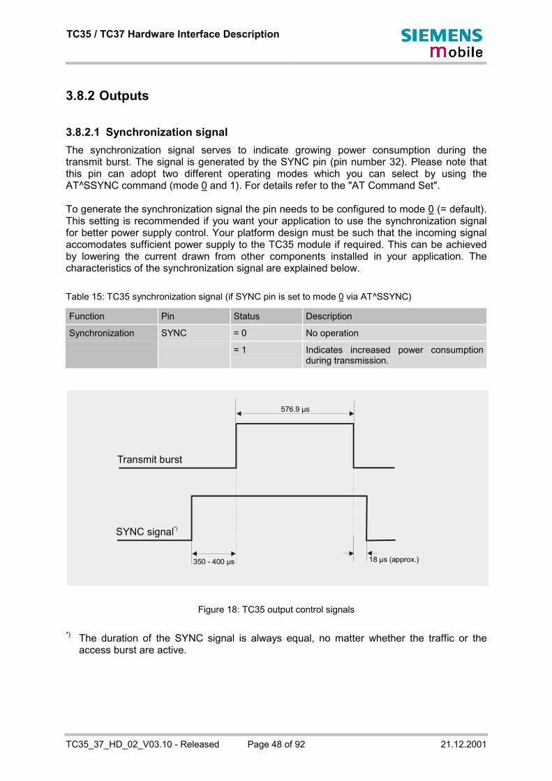
TC35 / TC37 Hardware Interface Description
TC35_37_HD_02_V03.10 - Released Page 48 of 92 21.12.2001
3.8.2 Outputs
3.8.2.1 Synchronization signalThe synchronization signal serves to indicate growing power consumption during thetransmit burst. The signal is generated by the SYNC pin (pin number 32). Please note thatthis pin can adopt two different operating modes which you can select by using theAT^SSYNC command (mode 0 and 1). For details refer to the "AT Command Set".
To generate the synchronization signal the pin needs to be configured to mode 0 (= default).This setting is recommended if you want your application to use the synchronization signalfor better power supply control. Your platform design must be such that the incoming signalaccomodates sufficient power supply to the TC35 module if required. This can be achievedby lowering the current drawn from other components installed in your application. Thecharacteristics of the synchronization signal are explained below.
Table 15: TC35 synchronization signal (if SYNC pin is set to mode 0 via AT^SSYNC)
Function Pin Status Description
= 0 No operationSynchronization SYNC
= 1 Indicates increased power consumptionduring transmission.
Figure 18: TC35 output control signals
*) The duration of the SYNC signal is always equal, no matter whether the traffic or theaccess burst are active.
Transmit burst
576.9 µs
18 µs (approx.)350 - 400 µs
SYNC signal*)

TC35 / TC37 Hardware Interface Description
TC35_37_HD_02_V03.10 - Released Page 49 of 92 21.12.2001
3.8.2.2 Using the SYNC pin to control a status LEDAs an alternative to generating the synchronization signal, the SYNC pin can be used tocontrol a status LED on your application platform.
To avail of this feature you need to set the SYNC pin to mode 1 by using the AT^SSYNCcommand. For details see the "AT Command Set".
When controlled from the SYNC pin the LED can display the following functions:
Table 16: Modes of the LED and associated functions
LED mode Function
Off *) TC35/TC37 is off, in SLEEP, Alarm or Charge-only mode.
600 ms On / 600ms Off *) No SIM card inserted or no PIN entered, or network search in progress,or ongoing user authentication, or network login in progress.
75ms On / 3s Off *) Logged to network (monitoring control channels and user interactions).No call in progress.
On Depending on type of call:Voice call: Connected to remote party.Data call: Connected to remote party or exchange of parameters whilesetting up or disconnecting a call.
*) LED Off = SYNC pin low. LED On = SYNC pin high (if LED is connected as illustrated in Figure 19)
To operate the LED a buffer, e.g. a transistor or gate, must be included in your application. Asample configuration can be gathered from Figure 19. Power consumption in the LED modeis the same as for the synchronization signal mode. For details see Table 18, pin number 32.
Figure 19: LED Circuit (Example)

TC35 / TC37 Hardware Interface Description
TC35_37_HD_02_V03.10 - Released Page 50 of 92 21.12.2001
1s
/RING0
URC
3.8.2.3 Behaviour of the RING0 lineThe behaviour of the /RING0 line depends on the type of the call received.• When a voice call comes in the /RING0 line goes low for 1s and high for another 4s.
Every 5 seconds the ring string is generated and sent over the RXD0 line.If there is a call in progress and call waiting is activated for a connected handset orhandsfree device, the /RING0 line switches to ground in order to generate acousticsignals that indicate the waiting call.
Figure 20: Incoming voice call
• Likewise, when a Fax or data call is received, /RING0 goes low. However, in contrast tovoice calls, the line remains low. Every 5 seconds the ring string is generated and sentover the RXD0 line.
Figure 21: Incoming data call
• All types of unsolicited result codes (URCs) also cause the/RING0 line to go low, however for 1 second only.For example, the GSM engine may be configured to outputa URC upon the receipt of an SMS. As a result, if this URCtype was activated with AT+CNMI=1,1, each incomingSMS causes the /RING0 line to go low.For more detailed information on URCs please refer the"TC3x AT Command Set".
Table 17: Ring signal
Function Pin Status Description
= 0 Indicates an incoming call or URC. If inSLEEP mode, the cellular deviceapplication is caused to wake up.
Ring indication /RING0
= 1 No operation
4s/RING0
4s
1s 1s 1sRing string
Ring string
Ring string
5s/RING0
Ring string
Ring string
Ring string
5s
TC35 / TC37 Hardware Interface Description
TC35_37_HD_02_V03.10 - Released Page 51 of 92 21.12.2001
3.9 Pin assignment
Please note that the reference voltages listed below are the values measured directly on theTC35 or TC37 module. They do not apply to the accessories connected.Table 18: Pin assignment
Function SignalName
PinNo.
I/O Signal Level Comment
1
2
3
4
VBATT+
5
I/(O) Input:
Vin = 3.3V...5.5V
Imax ≤ 2.0A at a return loss better than≥ 6dB (see Figure 41 and Figure 42)
Imax is valid only during uplink transmis-sion timeslot (e.g. TALK mode: Imax for577µs every 4.616ms)
Output: only valid when charging
6
7
8
9
Powersupply
GND
10
- Ground (0V)
Usage is mandatory
Five power supplypins have to be con-nected in parallel dueto peak current up to2A
Voltage must staywithin the min/maxvalues, including volt-age drop, ripple,spikes. See alsoTable 29.
11Charger POWER
12
I Vin = 5.5V...8V transformer plug
Vin = 5.5V...8V regulated plug
Imax = 550mA
internal Pull Down (100kΩ)
If unused keep pinopen
Supplyvoltage forexternalapplication
VDD 13 O IDLE / TALK mode:
Vout = 2.9V ±3% @ 70mA, VBatt = 4.2Vand Tamb typ = 25°C
Vout = 2.9V ±3% @ 20mA, VBatt = 4.8Vand Tamb typ = 25°C
Imax = 70mA
Power Down mode: Vout = 0V
Cload max,extern = 1µF
Can be used, forexample, to connect alevel converter or apull-up resistor. Notrecommended forcomponents operatedby pulse current.
If unused keep pinopen.
Voltage is applied60ms 100ms afterIGT was driven low.
Batterytempera-ture
AKKU_TEMP
14 I/O External NTC: RNTC = 10kΩ @ 25°CB = 3370 Kelvin ±3% connected to GND
IDLE/ TALK mode:Vout,MEAS(RNTC=10kΩ)=1.15V
Power Down mode:Vout = 0V (internal Pull Down)
If unused keep pinopen. If used: externalNTC should be in-stalled inside or nearbattery pack enablesthe charging algorithmand delivers tem-perature values

TC35 / TC37 Hardware Interface Description
TC35_37_HD_02_V03.10 - Released Page 52 of 92 21.12.2001
Function SignalName
PinNo.
I/O Signal Level Comment
Ignition /IGT 15 I IDLE/ TALK/ Power-Down mode:
Vout = 2.3VRout ≈ 220kΩVlow,max = 0.45V @ Iout = 10µAtlow ≥ 100ms (see Chapter 3.3!)
Signal: falling edge and hold for tlow
Usage is mandatory
Open drain/collectordriver is required topull down this pin topower on the GSMEngine
Signal is low active.
DSR0 16 O
/RING0 17 O
RxD0 18 O
TxD0 19 I
CTS0 20 O
RTS0 21 I
DTR0 22 I
RS232
DCD0 23 O
IDLE/ TALK mode:
Output:
Rout ≈ 1kΩVout,low,max = 0.2V @ I = 0.1mAVout,high,min = 2.25V @ I = -0.1mAVout,high,max = 2.76V
Input:
Ri ≥ 1MΩ (1kΩ serial resistor)Vin,low,min = -0.3V, Vi,l,max = 0.5VVin,high,min = 1.95V, Vi,h,max=3.3V
Power Down mode:
Signals are not defined.
Be aware of backward supply effects atthe inputs and outputs.
Application interfaceto control GSM engineusing AT commands
If unused keep outputpins open and con-nect input pins to VDDvia 10kΩ.
When a voice callcomes in RING0 goesactive low for 1s andinactive high for an-other 4s (alternating).An incoming data callalso causes RING0 togo active low, butwithout changing toinactive high. SeeChapter 3.8.2.3 formore details.
DCD0 and DTR0 linesare connected viainternal clamp diodesto 2.65V and GND

TC35 / TC37 Hardware Interface Description
TC35_37_HD_02_V03.10 - Released Page 53 of 92 21.12.2001
Function SignalName
PinNo.
I/O Signal Level Comment
CCIN 24 I IDLE / TALK mode:
SIM contact (active high)RPD = 100kΩ (internal Pull Down resis-tor to GND)Ri ≈ 10kΩVin,low,max = 0.4VVin,high,min = 2.15V, Vi,h,max = 3.3V
Power Down mode:Be aware of backward supply
All signals of the SIMinterface are pro-tected from electro-static discharge byusing spark gaps toGND and clampdiodes to 2.9V andGND
If a card is insertedCCIN has to be athigh level
If not used connect toCCVCC
CCRST 25 O Ri ≈ 47 Ω
External C = 1nF to CCGND required.This capacitor must be located close tothe SIM card reader.
CCIO 26 I/O Output:Ro ≈ 220 Ω (serial resistor)VOLmax = 0.2 V at I = 0.1 mAVOHmin = 2.25 V at I = -0.1 mAVOH = 2.76 V
Input:Ri ≈ 10 kΩVILmin=-0.3 V, VILmax = 0.5 VVIHmin = 1.95 V, VIHmax=3.3 V
Usage is mandatory
Signal levels accord-ing to GSM Rec. (2)
FFC must not exceed200mm to meet thetiming requirements ofGSM Rec. 11.10
CCCLK 27 O Output:Ro ≈ 220 Ω (serial resistor)VOLmax = 0.2 V at I = 0.1 mAVOHmin = 2.25 V at I = -0.1 mAVOH = 2.76 V
SIM
CCVCC 28 O CCVCCmin = 2.84VCCVCCmax = 2.96VImax = 20mA
External C ≥ 200nF to CCGND isrequired. This capacitor must belocated close to the SIM card reader.
Usage is mandatory
CCGND 29 O Ground (0V) Usage is mandatory.See Application noteSIM Interface for de-tails on grounding.

TC35 / TC37 Hardware Interface Description
TC35_37_HD_02_V03.10 - Released Page 54 of 92 21.12.2001
Function SignalName
PinNo.
I/O Signal Level Comment
RTCbackup
VDDLP 30 O
I
IDLE/TALK/Power Down mode ifVBATT+ connected:Vout = VBATT+ - 0.6VIout,max = 100mA
PD mode if VBATT+ disconnected:Vin = 2.0V...5.5VIin,max = 30µAtRTC,on ≈ 30s @ 100µF (typically)
If unused keep pinopen. See also chap-ter 3.3.4.
Powerdown
Foremergencyonly!
/PD 31 I/O IDLE/ TALK mode:
Input:
Ri = 1kΩ;Vin,low,max = 0.45V @ I = 0.1mA
input signal ~~~|______|~~~ activelow ≥ 3.5s
Watchdog Output:
Ri = 22kΩVout,low = 0.35V @ 0.01mAVout,high = 2.30V @ -0.01mA
fout = 0.5...2.0Hz
If unused keep pinopen
Open drain/collectordriver to GNDrequired.
/PD switches off theGSM engine. A lowpulse at pin IGTresets the GSMEngine and restartsthe system.
The /PD pin also indi-cates the watchdogfunction.
Synchroni-zation
SYNC 32 O IDLE/ TALK mode:
Ro = 1kΩVout,low,max = 0.2V @ 0.1mAVout,high,min = 2.25V @ -0.1mAVout,high,max = 2.76V
Power Down mode:be aware of backward supply
If unused keep pinopen
Indication of in-creased current con-sumption duringuplink transmissionburst

TC35 / TC37 Hardware Interface Description
TC35_37_HD_02_V03.10 - Released Page 55 of 92 21.12.2001
Function SignalName
PinNo.
I/O Signal Level Comment
EPP2 33 O
EPN2 34 O
Ri = 15Ω, (30kΩ if not active)Vomax = 3.7Vpp, no load,@ 3.14 dBm0:
f = 1024Hz,audio mode = 6,outBbcGain = 0,outCalibrate = 16384
If unused keep pinopen
Differential output,e.g. for external loud-speaker amplifier forhandsfree operation
EPP1 35 O
EPN1 36 O
Ri = 15Ω, (30kΩ if not active)Vomax = 3.7Vpp, no load,@ 3.14 dBm0:
f = 1024Hz,audio mode = 5,outBbcGain = 0,outCalibrate = 16384
If unused keep pinopen
Differential output,e.g. for internal ear-piece
MICP1 37 I
MICN1 38 I
Zi = 2kΩVimax = 1.03VppVsupply = 2.65V ( 0V if off ), RDC = 4kΩ
Keep unused inter-face open
Balanced input withswitchable micro-phone supply source,e.g. for internal micro-phone
MICP2 39 I
AudioInterface
MICN2 40 I
Zi = 2kΩVimax = 1.03VppVsupply = 2.65V ( 0V if off ), RDC = 4kΩ
Keep unused inter-face open
Balanced input withswitchable micro-phone supply source,e.g. for externalmicrophone forhandsfree operation
Explanation of signal names:P = positiveN = negative

TC35 / TC37 Hardware Interface Description
TC35_37_HD_02_V03.10 - Released Page 56 of 92 21.12.2001
4 Radio interfaceThe RF part of TC35 and TC37 is based on the Transceiver Chip SMARTi. The transceiverconsists of a heterodyne receiver part, an upconversion modulation loop transmitter, a RFPLL and fully integrated IF synthesizer.
4.1 Receiver
The receiver section of RF part provides the following features:• Two low noise RF mixers for optimal dual band architectures• Programmable Gain IF/Baseband amplifier strip by steps of 2dB• Quadrature IF demodulator• Differential I and Q outputs• Programmable output DC level• Automatic DC offset compensation
The signal received from the antenna first passes a gain programmable discrete low noiseamplifier (LNA) in the receiver chain. After external filtering the double balanced RF signal isdown converted to an intermediate frequency (IF) by a first mixer. The IF signal is passedthrough an external Surface Acoustic Wave (SAW) filter, which performs a rough channelselection. After that the signal is fed again into the receiver circuit to pass a digitallyprogrammable gain-controlled amplifier (PGC). Finally the amplified IF signal is demodulatedto baseband by a IQ demodulator. A differential offset introduced by the IQ demodulator iscompensated by a sample-and-hold circuit. The resulting differential I and Q basebandsignals are converted independently from analog to digital forming two 6.5Mbit/s datastreams.
4.2 Transmitter
The transmitter section of the RF part provides the following features:• Differential I and Q inputs• IF quadrature modulator• Integrated IF filters and down conversion mixer• Digital 250MHz Phase Frequency Detector• Programmable Charge pump current and phase detector polarity
The digital 10-bit I and Q baseband components (GMSK modulated and 8-timesoversampled) provided by GSM baseband processor are converted in parallel from digital toanalog. The resulting analog differential baseband signal is fed to the input of a quadratureamplitude modulator followed by the up-conversion loop. This up-conversion loopconfiguration converts the IF-band signal to the desired radio frequency in the 900MHz or1.8GHz band. Finally a RF power module (Dual band) amplifies the RF signal to the requiredpower. Ramping of the power amplifier is performed software controlled by 10-bit controlvalues.

TC35 / TC37 Hardware Interface Description
TC35_37_HD_02_V03.10 - Released Page 57 of 92 21.12.2001
4.3 Antenna interface (antenna reference point ARP)
There are no special antenna systems specified for TC35 and TC37. All RF interfaces(connectors or pad) have an impedance of 50Ω with an SWR ≤2. TC35 and TC37 arecapable of sustaining a total mismatch at the antenna connector or pad when transmittingwith power control level for maximum RF Power.Table 19: Return loss
State of module Return loss of module Recommended return loss of application
Receive 8dB min higher than 12dB min
Transmit not applicable higher than 12dB min
Idle 5dB max not applicable
4.3.1 Options of connecting the antenna
In order to suit the physical design of individual applications SIEMENS cellular enginesprovide various RF interfaces to connect an external or internal antenna:
• On TC35, a GSC connector is assembled on the PCB. The GSC connector is made byMurata. Though present on the board, the antenna pad is not connected.
Figure 22: Antenna connector circuit on TC35
• TC37 comes with a gold plated antenna pad and a switching coax connector. Bothoptions can be applied alternatively: Whenever an antenna is plugged into the coaxconnector the switch opens, thus disconnecting the pad. Vice versa, removing theantenna from the switch connector closes the switch and thus, activates the pad.
Figure 23: Antenna connector circuit on TC37
GSC connector (from Murata)
TRX Output
L (27nH)
Matching circuit
Antenna pad
Coaxicon connector (from AMP)
TR X output

TC35 / TC37 Hardware Interface Description
TC35_37_HD_02_V03.10 - Released Page 58 of 92 21.12.2001
4.3.2 Description of antenna ports and connectors
Table 20: Signals available on GSC jack
Signal name Pin I/O Description Parameter
RF Internal I/O RF input and output Z = 50 Ω
GND External X Ground connection
Table 21: Signals available on antenna pad / coaxicon connector
Signal name Pin I/O Description Parameter
RF Pad I/O RF input and output, can be deactivatedwhen the jack is connected
RF Internal I/O RF input and output Z = 50 Ω
GND External X Ground connection
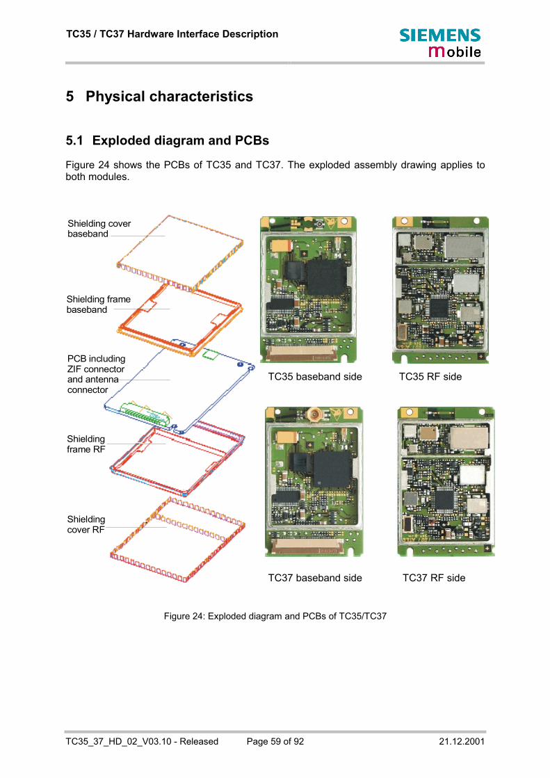
TC35 / TC37 Hardware Interface Description
TC35_37_HD_02_V03.10 - Released Page 59 of 92 21.12.2001
Shielding coverbaseband
Shielding framebaseband
PCB includingZIF connector and antennaconnector
Shielding frame RF
Shielding cover RF
5 Physical characteristics
5.1 Exploded diagram and PCBs
Figure 24 shows the PCBs of TC35 and TC37. The exploded assembly drawing applies toboth modules.
TC35 baseband side TC35 RF side
TC37 baseband side TC37 RF side
Figure 24: Exploded diagram and PCBs of TC35/TC37

TC35 / TC37 Hardware Interface Description
TC35_37_HD_02_V03.10 - Released Page 60 of 92 21.12.2001
5.2 Mechanical dimensions of TC35 and TC37
Figure 25 shows the RF part of TC35 and TC37 and provides an overview of the board'smechanical dimensions. For further details see Figure 26.
Size: 54.5+0.2 x 36+0.2 x 6.85+0.35 mm (height of antenna connector not considered)Weight: approx. 18g
Figure 25: TC35 / TC37 view of RF part

TC35 / TC37 Hardware Interface Description
TC35_37_HD_02_V03.10 - Released Page 61 of 92 21.12.2001
0,00 = Reference point All dimensions stated in millimeter
Figure 26: Mechanical dimensions of TC35

TC35 / TC37 Hardware Interface Description
TC35_37_HD_02_V03.10 - Released Page 62 of 92 21.12.2001
0,00 = Reference point All dimensions stated in millimeter
Figure 27: Mechanical dimensions of TC37

TC35 / TC37 Hardware Interface Description
TC35_37_HD_02_V03.10 - Released Page 63 of 92 21.12.2001
5.3 Mounting TC35/TC37 onto the application platform
For the cellular application to operate reliably it is essential that the GSM engine is securelyattached to the host housing.
The TC35/TC37 board provides three mounting holes. To properly mount it to the hostdevice you can use M1.6 or M1.8 screws plus suitable washers. The maximum diameter ofthe screw head incl. the washer must not exceed 4 mm.
To prevent mechanical damage, be careful not to force, bend or twist the GSM engine. Besure it is positioned flat against the host device.
Avoid placing the TC35 or TC37 board tightly to the host device. Instead, it is recommendedto set spacers between the module and the host device. If your design approach does notallow for spacers make sure the host device provides an opening for the RF part.
5.3.1 Mounting TC35
Figure 28: Mounting TC35 (example)
Shielding coverRF part
Do not use this pad
Mounting hole
GSC connector
Mounting hole
Long mounting hole
Shielding coverbaseband part
ZIF connector

TC35 / TC37 Hardware Interface Description
TC35_37_HD_02_V03.10 - Released Page 64 of 92 21.12.2001
5.3.2 Mounting TC37
Caution: The antenna pad of TC37 is located close to the mounting hole. If youconnect your antenna to the pad only insert an insulated (nylon) screw, orrather leave the hole open while using a clamp or clip to secure TC37 onto thehost device.
Figure 29: Mounting TC37 (example)
Shielding coverRF part
Antenna pad Mounting hole (avoid using this hole if antenna connects to pad)
Switching connector
Mounting hole
Long mounting hole
Shielding coverbaseband part
ZIF connector

TC35 / TC37 Hardware Interface Description
TC35_37_HD_02_V03.10 - Released Page 65 of 92 21.12.2001
5.3.3 Positioning labels on TC35 and TC37
The product label is divided into two sections which are identical in content. The upper labelcan be placed on the customer application. The second label is positioned on the shieldingcover of the RF part as shown below.
Figure 30: Positioning labels
Figure 31: Label dimensions
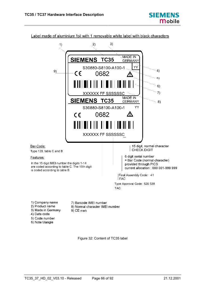
TC35 / TC37 Hardware Interface Description
TC35_37_HD_02_V03.10 - Released Page 66 of 92 21.12.2001
Figure 32: Content of TC35 label

TC35 / TC37 Hardware Interface Description
TC35_37_HD_02_V03.10 - Released Page 67 of 92 21.12.2001
5.4 ZIF connector
This chapter provides specifications and handling instructions for the 40-pin ZIF connectorand the Flat Flexible Cable (FFC) used to connect the GSM engine to the host application.
The ZIF (zero insertion force) design allows to easily fasten or remove the cable without theneed for special tools. Simply insert the FFC cable into the open socket without using anypressure. Then carefully close the socket lid until the contacts of the socket grip the cablecontacts.
Table 22: Electrical and mechanical characteristics of the ZIF connector
Parameter Specification (40 pin ZIF connector)
Number of Contacts 40
Quantity delivered 2000 connectors per tape & reel
Voltage 50V
Current Rating 0.4A max per contact
Resistance 0.05 Ohm per contact
Dielectric Withstanding Voltage 200V RMS min
Operating Temperature -40°C...+85°C
Contact Material Phosphor bronze (tin-lead plated)
Insulator Material PPS, natural color
Slider Material PPS, natural color
FFC/FPC Thickness 0.3mm ±0.05mm (0.012" ±0.002")
Profile Height 2.00mm
Dimension A 24
Dimension B 19.5
Dimension C 26.2
Maximum connection cycles 50
Cable FFC (Flat Flexible Cable), max. length 200mm from SIM interface

TC35 / TC37 Hardware Interface Description
TC35_37_HD_02_V03.10 - Released Page 68 of 92 21.12.2001
5.4.1 Mechanical dimensions of the ZIF connector
Figure 33: Mechanical dimensions of ZIF connector
Figure 34: PCB ZIF connector

TC35 / TC37 Hardware Interface Description
TC35_37_HD_02_V03.10 - Released Page 69 of 92 21.12.2001
5.5 Antenna design
As stated earlier, TC35 and TC37 are distinguished by the various options of connecting theantenna. This chapter provides technical specifications and ordering information for eachsolution.
Note: Be sure that all peripherals are applied according to the manufacturer's antennaspecifications. For internal antenna equipment you are advised to use the servicesof a consultant or full-service house.
A 27nH inductor to ground provides additional ESD protection for the antennaconnector. To protect the inductor from damage no DC voltage must be applied tothe antenna circuit.
5.5.1 GSC antenna connector on TC35
TC35 uses a GSC connector to establish the RF connection to the host application. Belowplease find brief ordering information to help you retrieve further details from themanufacturer MuRata, e.g. under http://www.murata.com.
Description MuRata part number
Male connector mounted on TC35 MM9329-2700
Matching female connectors suited for individual cable assembly• Right-angle flexible cable• Right-angle flexible cable• Right-angle semirigid cable
MXTK88xxxxMXTK92xxxxMXTK91xxxx
Engagement/disengagement tool type P/N M22001 Please use product name foryour order: P/N M22001
The physical dimensions and maximum mechanical stress limits can be gathered from thetable and the figures below. To securely fasten or remove the antenna cable MuRatarecommends to use the P/N M22001 engagement/disengagement tool.
Table 23: Ratings and characteristics of the GSC antenna connector
Item Specification
Frequency range DC to 6GHz
VSWR 1.2 max. (DC to 3 GHz), 1.3 max. 3GHz to 6GHz)
Nominal impedance 50Ω
Temperature range -40°C to +90°C
Contact resistance 15mΩ max.
Withstanding voltage AC300V
Insulation resistance 500MΩ min.

TC35 / TC37 Hardware Interface Description
TC35_37_HD_02_V03.10 - Released Page 70 of 92 21.12.2001
Item Specification
Material and finish• Center contact:• Outer contact:• Insulator:
Material: Finish:Copper alloy Gold platedCopper alloy Silver platedEngineering plastic None
Figure 35: Mechanical dimensions of MuRata GSC connector (in mm)
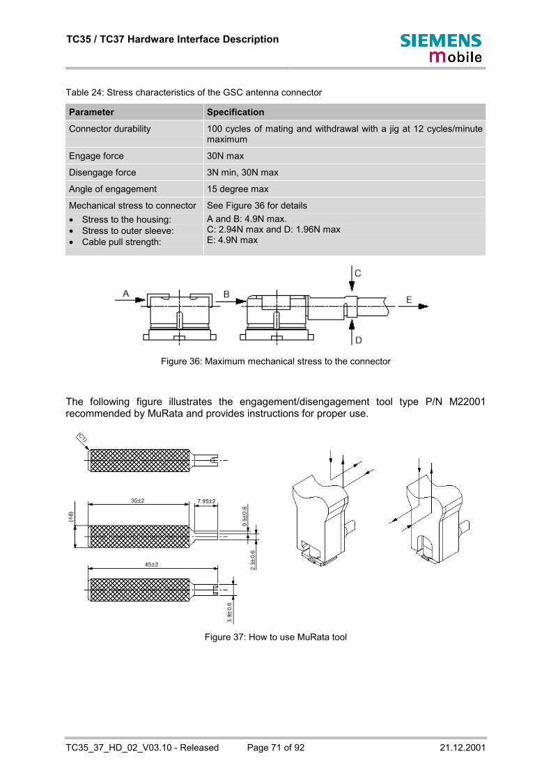
TC35 / TC37 Hardware Interface Description
TC35_37_HD_02_V03.10 - Released Page 71 of 92 21.12.2001
Table 24: Stress characteristics of the GSC antenna connector
Parameter Specification
Connector durability 100 cycles of mating and withdrawal with a jig at 12 cycles/minutemaximum
Engage force 30N max
Disengage force 3N min, 30N max
Angle of engagement 15 degree max
Mechanical stress to connector• Stress to the housing:• Stress to outer sleeve:• Cable pull strength:
See Figure 36 for detailsA and B: 4.9N max.C: 2.94N max and D: 1.96N maxE: 4.9N max
Figure 36: Maximum mechanical stress to the connector
The following figure illustrates the engagement/disengagement tool type P/N M22001recommended by MuRata and provides instructions for proper use.
Figure 37: How to use MuRata tool

TC35 / TC37 Hardware Interface Description
TC35_37_HD_02_V03.10 - Released Page 72 of 92 21.12.2001
5.5.2 Using antenna eqipment from other manufacturers
For your product to meet individual design or technical requirements, you may decide tochoose antenna equipment from suppliers other than MuRata.
When selecting a suitable antenna your considerations should also include the requirementsof electromechanical valence. To achieve best performance it is essential to minimize thevalence potential delta levels of dissimilar metal mating surfaces. Therefore the material ofthe antenna cable plug must be compatible with the material of the GSC receptacle on theGSM engine, i.e. it should belong to the same group in the electromechanical series. Thematerial of the GSC connector on TC35 in specified in Table 23.
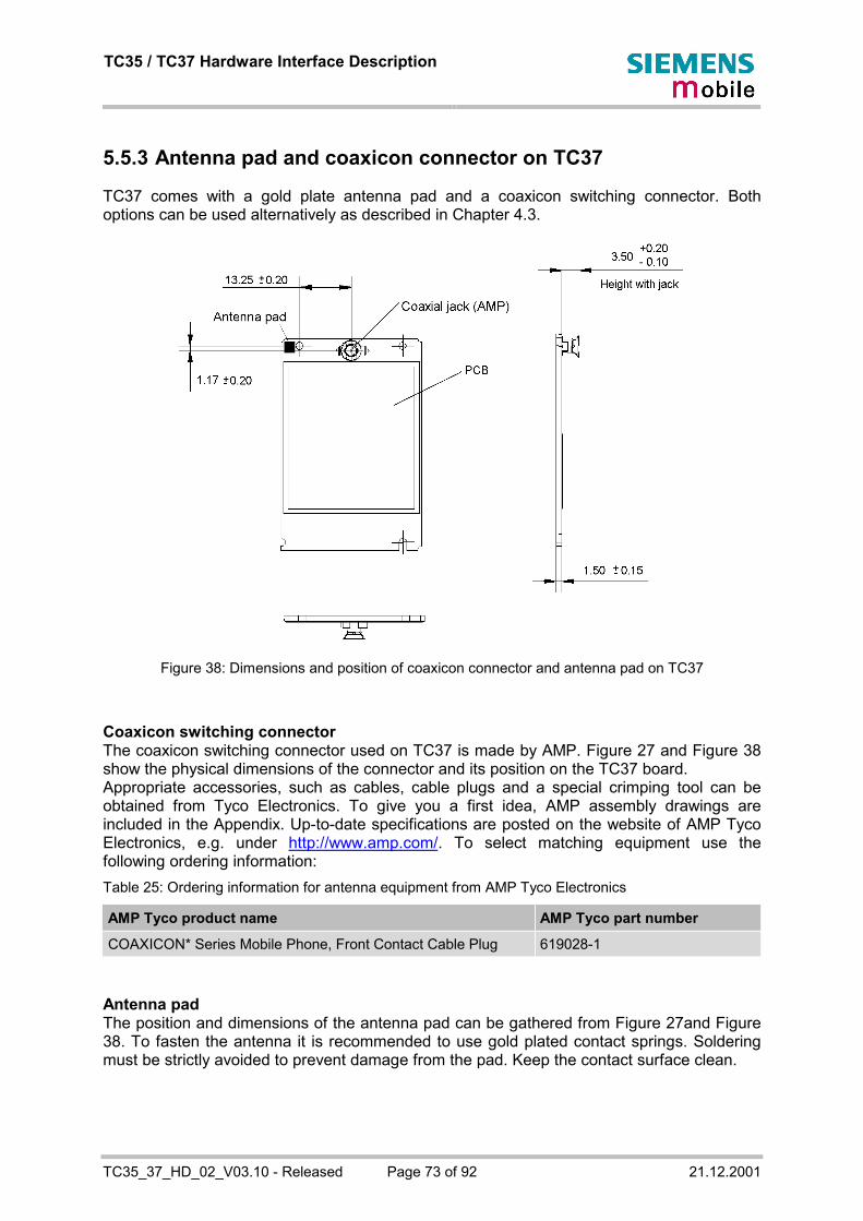
TC35 / TC37 Hardware Interface Description
TC35_37_HD_02_V03.10 - Released Page 73 of 92 21.12.2001
5.5.3 Antenna pad and coaxicon connector on TC37
TC37 comes with a gold plate antenna pad and a coaxicon switching connector. Bothoptions can be used alternatively as described in Chapter 4.3.
Figure 38: Dimensions and position of coaxicon connector and antenna pad on TC37
Coaxicon switching connectorThe coaxicon switching connector used on TC37 is made by AMP. Figure 27 and Figure 38show the physical dimensions of the connector and its position on the TC37 board.Appropriate accessories, such as cables, cable plugs and a special crimping tool can beobtained from Tyco Electronics. To give you a first idea, AMP assembly drawings areincluded in the Appendix. Up-to-date specifications are posted on the website of AMP TycoElectronics, e.g. under http://www.amp.com/. To select matching equipment use thefollowing ordering information:Table 25: Ordering information for antenna equipment from AMP Tyco Electronics
AMP Tyco product name AMP Tyco part number
COAXICON* Series Mobile Phone, Front Contact Cable Plug 619028-1
Antenna padThe position and dimensions of the antenna pad can be gathered from Figure 27and Figure38. To fasten the antenna it is recommended to use gold plated contact springs. Solderingmust be strictly avoided to prevent damage from the pad. Keep the contact surface clean.

TC35 / TC37 Hardware Interface Description
TC35_37_HD_02_V03.10 - Released Page 74 of 92 21.12.2001
6 Electrical, temperature and radio characteristics
6.1 Absolute maximum ratings
Absolute maximum ratings for supply voltage and voltages on digital and analog pins ofTC35 and TC37 are listed in Table 26. Exceeding these values will cause permanentdamage to the GSM Engine. The supply current must be limited accordingly. The safetystatus of the power supply is subject to SELV (as defined by EN60950)
Table 26: Absolute maximum ratings
Parameter Min Max Unit
Peak current of power supply 0 4.0 A
RMS current of power supply (during one TDMA-frame) 0 0.5 A
Voltage on digital pins *) -0.3 3.3 V
Voltage on analog pins *) -0.3 3.0 V
*)Valid only in IDLE and TALK mode, if in Power Down mode absolute maximum ratings are ± 0.25 V.
6.2 Operating conditions
Table 27: Operating conditions
Parameter Min Typ Max Unit
Ambient temperature -20 25 55 °C
Supply voltage VBATT+ 3.3 4.2 5.5 V
6.3 Temperature conditions
Test conditions were specified in accordance with IEC 60068-2 (still air).Table 28: Temperature conditions
Parameter Min Typ Max Unit
Ambient temperature (regarding GSM 11.10) -20 25 55 °C
Restricted operation *) -25 to -20 55 to 70 °C
Automatic shutdown: if application is not battery poweredif application is battery powered
-25-15
>70**)
>60**)°C°C
Storage temperature -40 +85 °C
Charging temperature (software controlled fast charging) 0 +45 °C
*) GSM engine is operational, but deviations from the GSM specification may occur.**) Limited performance if VBATT+ max <4.0V and PCL5 is required at Tamb max = 70°

TC35 / TC37 Hardware Interface Description
TC35_37_HD_02_V03.10 - Released Page 75 of 92 21.12.2001
6.4 Power supply ratings
Table 29: Power supply ratings
Parameter Description Conditions Min Typ Max Unit
Supply voltage Reference point on VBATT+contact pad
Voltage must stay within themin/max values, includingvoltage drop, ripple, spikes.
3.3 4.2 5.5 V
Voltage drop duringtransmit burst
Normal condition, power controllevel for Pout max
400 mV
VBATT+
Voltage ripple Normal condition, power controllevel for Pout max@ f<200kHz@ f>200kHz
502
mV
Power Down mode 50 100 µA
SLEEP mode 3 3.5 mA
IDLE mode GSM 10 20 mA
Average supplycurrent
TALK mode GSM 300 400 mA
IBATT+
Peak supply current(during 577µs trans-mission slot every4.6ms)
Power control level for Pout maxImax
See Table 32and Table 33
A
Charging current Li-Ion battery pack 500 mAICHARGE
Trickle charging Ubattery 0...3.6V 9.0 mA
6.4.1 Drop definition
Due to peak currents of I = 2 A, a GSM transmission burst may cause considerable voltagedrop. Further losses may result from the internal resistance of the external power supplylines. As specified above, the supply voltage VBATT+ must not fall below 3.3 V at any time,while the voltage drop must not exceed 400 mV.In order to minimize voltage drop during transmission bursts, use an FFC cable as short aspossible and apply a low-impedance power supply.

TC35 / TC37 Hardware Interface Description
TC35_37_HD_02_V03.10 - Released Page 76 of 92 21.12.2001
Typical Current Consumption Burst
0,00
0,20
0,40
0,60
0,80
1,00
1,20
1,40
1,60
1,80
2,00
0 1 2 3 4 5 6 7 8 9 10 11 12 13 14 15 16 17 18 19 20
Pow er control level
peak
cur
rent
/ A
GSM900
GSM1800
Typical Current Consumption Average
0,05
0,08
0,10
0,13
0,15
0,18
0,20
0,23
0,25
0,28
0,30
0 1 2 3 4 5 6 7 8 9 10 11 12 13 14 15 16 17 18 19 20
Pow er control level
Cur
rent
/ A
GSM 900
DCS 1800
6.4.2 Current consumption during transmit burst
The diagrams in Figure 39 through Figure 40 illustrate the peak current consumption of theapplication caused during a transmit burst. The peak current is shown vs. the power level forGSM900/1800 and vs. the return loss of the antenna. All measurements have beenperformed at 25°C and 4.2V (reference points used on module: test points on ZIFconnector). Changing the conditions, e.g. in terms of temperature or voltage, will causedifferent results. The current will be maximized when the maximum supply voltage is usedtogether with a total reflection at the RF interface. Using a supply voltage higher than 4.3V atPCL5 GSM 900 lets the peak current rise by about 150mA, due to higher RF output power.
Figure 39: Typical current (peak) vs power control level
Figure 40: Typical current (average) vs power control level
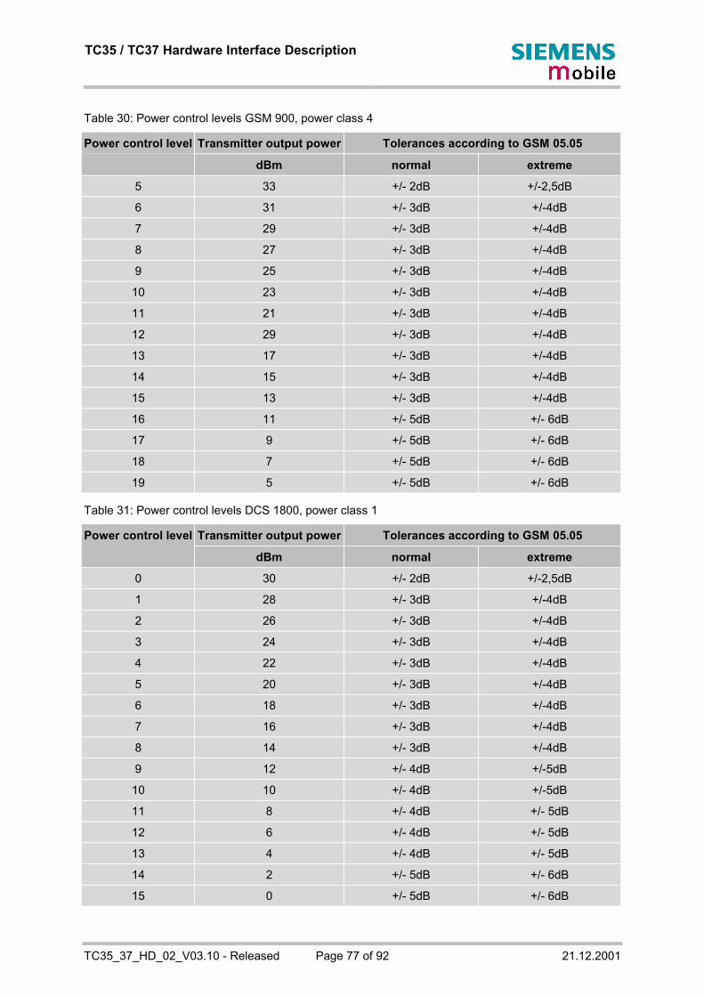
TC35 / TC37 Hardware Interface Description
TC35_37_HD_02_V03.10 - Released Page 77 of 92 21.12.2001
Table 30: Power control levels GSM 900, power class 4
Transmitter output power Tolerances according to GSM 05.05Power control level
dBm normal extreme
5 33 +/- 2dB +/-2,5dB
6 31 +/- 3dB +/-4dB
7 29 +/- 3dB +/-4dB
8 27 +/- 3dB +/-4dB
9 25 +/- 3dB +/-4dB
10 23 +/- 3dB +/-4dB
11 21 +/- 3dB +/-4dB
12 29 +/- 3dB +/-4dB
13 17 +/- 3dB +/-4dB
14 15 +/- 3dB +/-4dB
15 13 +/- 3dB +/-4dB
16 11 +/- 5dB +/- 6dB
17 9 +/- 5dB +/- 6dB
18 7 +/- 5dB +/- 6dB
19 5 +/- 5dB +/- 6dB
Table 31: Power control levels DCS 1800, power class 1
Transmitter output power Tolerances according to GSM 05.05Power control level
dBm normal extreme
0 30 +/- 2dB +/-2,5dB
1 28 +/- 3dB +/-4dB
2 26 +/- 3dB +/-4dB
3 24 +/- 3dB +/-4dB
4 22 +/- 3dB +/-4dB
5 20 +/- 3dB +/-4dB
6 18 +/- 3dB +/-4dB
7 16 +/- 3dB +/-4dB
8 14 +/- 3dB +/-4dB
9 12 +/- 4dB +/-5dB
10 10 +/- 4dB +/-5dB
11 8 +/- 4dB +/- 5dB
12 6 +/- 4dB +/- 5dB
13 4 +/- 4dB +/- 5dB
14 2 +/- 5dB +/- 6dB
15 0 +/- 5dB +/- 6dB

TC35 / TC37 Hardware Interface Description
TC35_37_HD_02_V03.10 - Released Page 78 of 92 21.12.2001
The figures below show the typical peak current in dependency of load mismatch during atransmit burst with the power control level for maximum RF power. To achieve optimumperformance the return loss of the customer application should be better than 10dB.
Figure 41: Typical current consumption for GSM 900, power level = 5
Figure 42: Typical current consumption for DCS1800, power level = 0
Typical current consumption GSM900 vs. load impedancepower level = 5
1,51,61,71,81,92,02,12,22,32,42,52,62,72,8
0 2 4 6 8 10 12 14 16 18 20
return loss of the load (application) / dB
peak
cur
rent
/ A
Typical current consumption DCS 1800 vs. load impedancepower level = 0
1,0
1,1
1,2
1,3
1,4
1,5
1,6
1,7
1,8
1,9
2,0
0 2 4 6 8 10 12 14 16 18 20
return loss of the load (application) / dB
peak
cur
rent
/ A
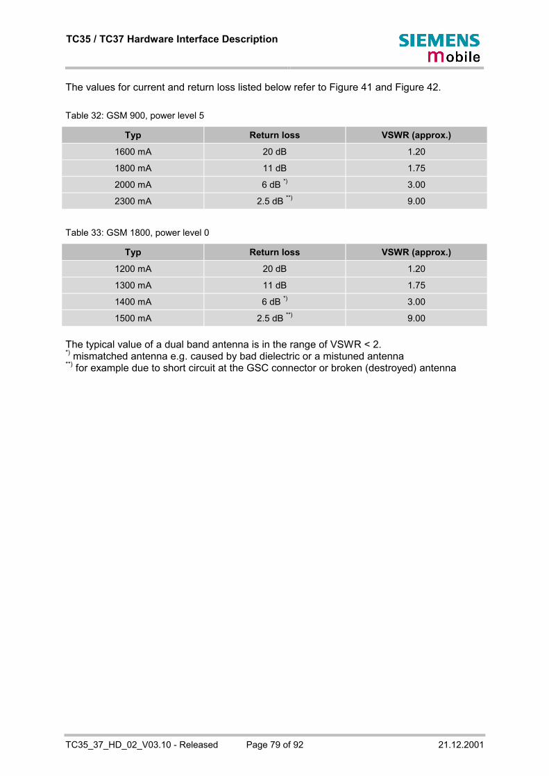
TC35 / TC37 Hardware Interface Description
TC35_37_HD_02_V03.10 - Released Page 79 of 92 21.12.2001
The values for current and return loss listed below refer to Figure 41 and Figure 42.
Table 32: GSM 900, power level 5
Typ Return loss VSWR (approx.)
1600 mA 20 dB 1.20
1800 mA 11 dB 1.75
2000 mA 6 dB *) 3.00
2300 mA 2.5 dB **) 9.00
Table 33: GSM 1800, power level 0
Typ Return loss VSWR (approx.)
1200 mA 20 dB 1.20
1300 mA 11 dB 1.75
1400 mA 6 dB *) 3.00
1500 mA 2.5 dB **) 9.00
The typical value of a dual band antenna is in the range of VSWR < 2.*) mismatched antenna e.g. caused by bad dielectric or a mistuned antenna**) for example due to short circuit at the GSC connector or broken (destroyed) antenna

TC35 / TC37 Hardware Interface Description
TC35_37_HD_02_V03.10 - Released Page 80 of 92 21.12.2001
6.5 Electrical characteristics of the voiceband part
6.5.1 Setting audio parameters by AT commands
Each audio mode is assigned a separate set of parameters. The audio modes 2 to 6 can beadjusted according to the parameters listed below. Audio mode 1 is the default configurationwhich cannot be modified.Table 34: Audio parameters adjustable by AT command
Parameter Influence to Range Gain range Calculation
inBbcGain MICP/MICN analogue amplifier gainof baseband controller before ADC
0...7 0...42dB 6dB steps
inCalibrate digital attenuation of input signalafter ADC
0...32767 -∞...0dB 20 * log(inCalibrate/32768)
outBbcGain EPP/EPN analogue output gain ofbaseband controller after DAC
0...3 0...-18dB 6dB steps
outCalibrate[n]n = 0...4
digital attenuation of output signalafter speech decoder, beforesummation of sidetone and DAC
present for each volume step[n]
0...32767 -∞...+6dB 20 * log (2 *outCalibrate[n]/32768)
sideTone digital attenuation of sidetone
is corrected internally by outBbcGainto obtain a constant sidetoneindependent of output volume
0...32767 -∞...0dB 20 * log(sideTone/32768)
Note: The inCalibrate, outCalibrate and sideTone accept also values from 32768 to 65535.These values are internally truncated to 32767.The following figure illustrates how the signal path can be influenced by varying the ATcommand parameters.
A
D
A
D
-∞...0dB
speechcoder
(0dB; -6db,-12dB; -18dB)
+0..42dB in6dB-steps
1k
1k
1k
1k
2,65V
10uF
6,8R
6,8R+
sideTone
AT - parameter
outCalibrate[n]n = 0...4
inCalibrate
inBbcGain
outBbcGain
speechdecoder
Figure 43: AT audio programming model
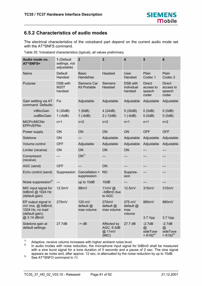
TC35 / TC37 Hardware Interface Description
TC35_37_HD_02_V03.10 - Released Page 81 of 92 21.12.2001
6.5.2 Characteristics of audio modes
The electrical characteristics of the voiceband part depend on the current audio mode setwith the AT^SNFS command.Table 35: Voiceband characteristics (typical), all values preliminary
Audio mode no.AT^SNFS=
1 (Defaultsettings, notadjustable)
2 3 4 5 6
Name DefaultHandset
BasicHandsfree
Headset UserHandset
PlainCodec 1
PlainCodec 2
Purpose DSB withM20Thandset
Siemens CarKit Portable
SiemensHeadset
DSB withindividualhandset
Directaccess tospeechcoder
Directaccess tospeechcoder
Gain settting via ATcommand. Defaults:
inBbcGainoutBbcGain
Fix
5 (30dB)1 (-6dB)
Adjustable
1 (6dB)1 (-6dB)
Adjustable
4 (24dB)2 (-12dB)
Adjustable
5 (30dB)1 (-6dB)
Adjustable
0 (0dB)0 (0dB)
Adjustable
0 (0dB)0 (0dB)
MICPn/MICNnEPPn/EPNn
n=1 n=2 n=2 n=1 n=1 n=2
Power supply ON ON ON ON OFF OFF
Sidetone ON --- Adjustable Adjustable Adjustable Adjustable
Volume control OFF Adjustable Adjustable Adjustable Adjustable Adjustable
Limiter (receive) ON ON ON ON --- ---
Compressor(receive)
--- ON1) --- --- --- ---
AGC (send) OFF --- ON --- --- ---
Echo control (send) Suppression Cancellation +suppression
NO Suppres-sion
--- ---
Noise suppression2) --- up to 10dB 10dB --- --- ---
MIC input signal for0dBm0 @ 1024 Hz(default gain)
12.5mV 98mV 11mV @-3dBm0 dueto AGC
12.5mV 315mV 315mV
EP output signal inmV rms. @ 0dBm0,1024 Hz, no load(default gain);@ 3.14 dBm0
275mV 120 mVdefault @max volume
270mVdefault @max volume
275 mVdefault @maxvolume
880mV
3.7 Vpp
880mV
3.7 Vpp
Sidetone gain atdefault settings
27.7dB -∞ dB Affected byAGC, 9.3dB@ 11mV(MIC)
27.7 dB -2.7dB@sideTone= 81923)
-2.7dB@sideTone= 81923)
1) Adaptive, receive volume increases with higher ambient noise level.2) In audio modes with noise reduction, the microphone input signal for 0dBm0 shall be measured
with a sine burst signal for a tone duration of 5 seconds and a pause of 2 sec. The sine signalappears as noise and, after approx. 12 sec, is attenuated by the noise reduction by up to 10dB.
3) See AT^SNFO command in /1/.

TC35 / TC37 Hardware Interface Description
TC35_37_HD_02_V03.10 - Released Page 82 of 92 21.12.2001
Note: With regard to acoustic shock, the cellular application must be designed to avoidsending false AT commands that might increase amplification, e.g. for a highsensitive earpiece. A protection circuit should be implemented in the cellularapplication.
6.5.3 Voiceband receive path
The values specified below were tested to 1kHz and 0dB gain stage, unless otherwisestated.
gs = 0dB means audio mode = 5 for EPP1 to EPN1 and 6 for EPP2 to EPN2, inBbcGain= 0,inCalibrate = 32767, outBbcGain = 0, OutCalibrate = 16384, sideTone = 0.
Table 36: Voiceband receive path
Parameter Min Typ Max Unit Test condition / remark
Differential outputvoltage (peak to peak)
3.33 3.7 4.07 V from EPPx to EPNxgs = 0dB @ 3.14 dBm0
Differential output gainsettings (gs) at 6dBstages (outBbcGain)
-18 0 dB
fine scaling by DSP(outCalibrate)
-∞ 0 dB
Output differentialDC offset
100 mV gs = 0dB, outBbcGain = 0 and -6dB
Differential outputresistance
13 15 Ω from EPPx to EPNx
Absolute gain accuracy 0.8 dB Variation due to change in VDD,temperature and life time
Attenuation distortion 1 dB for 300...3900Hz,
@ EPPx/EPNx (333Hz) /
@ EPPx/EPNx (3.66kHz)
Out-of-banddiscrimination
60 dB for f > 4kHz with in-band test signal@ 1kHz and 1kHz RBW
gs = gain setting
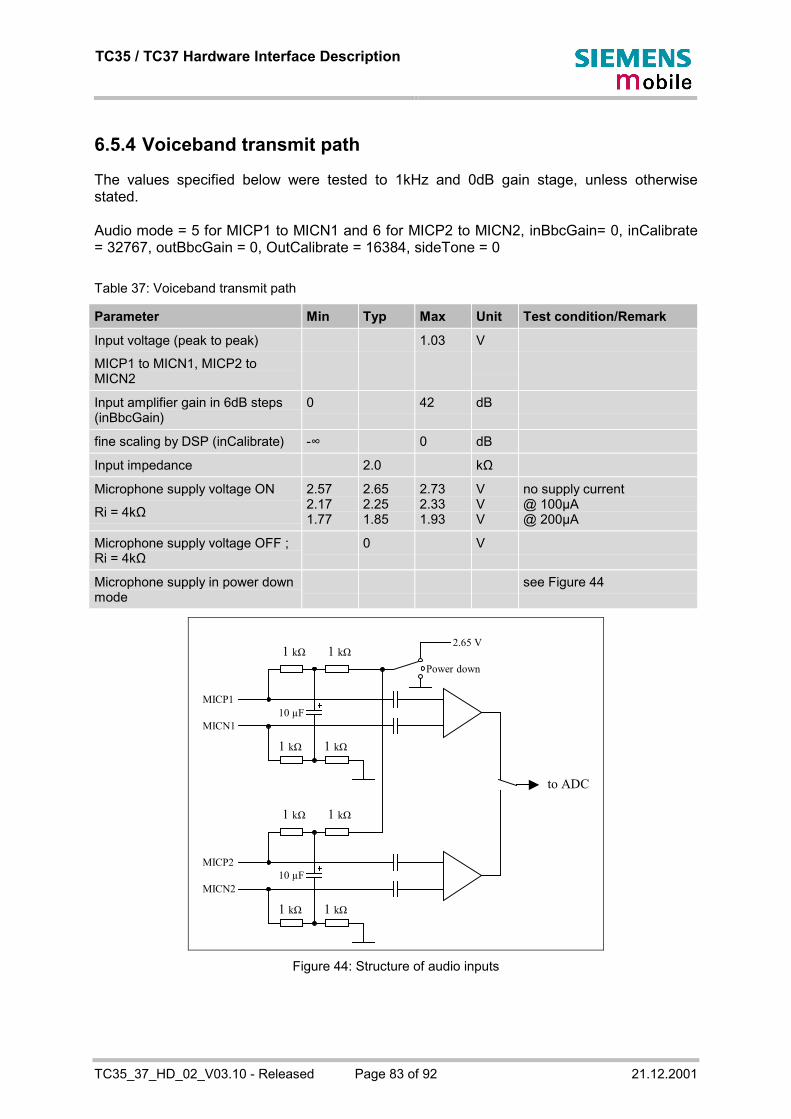
TC35 / TC37 Hardware Interface Description
TC35_37_HD_02_V03.10 - Released Page 83 of 92 21.12.2001
6.5.4 Voiceband transmit path
The values specified below were tested to 1kHz and 0dB gain stage, unless otherwisestated.
Audio mode = 5 for MICP1 to MICN1 and 6 for MICP2 to MICN2, inBbcGain= 0, inCalibrate= 32767, outBbcGain = 0, OutCalibrate = 16384, sideTone = 0
Table 37: Voiceband transmit path
Parameter Min Typ Max Unit Test condition/Remark
Input voltage (peak to peak)
MICP1 to MICN1, MICP2 toMICN2
1.03 V
Input amplifier gain in 6dB steps(inBbcGain)
0 42 dB
fine scaling by DSP (inCalibrate) -∞ 0 dB
Input impedance 2.0 kΩ
Microphone supply voltage ON
Ri = 4kΩ
2.572.171.77
2.652.251.85
2.732.331.93
VVV
no supply current@ 100µA@ 200µA
Microphone supply voltage OFF ;Ri = 4kΩ
0 V
Microphone supply in power downmode
see Figure 44
2.65 V
to ADC
Power down
MICP1
MICN1
1 kΩ 1 kΩ
1 kΩ 1 kΩ
10 µF
MICP2
MICN2
1 kΩ 1 kΩ
1 kΩ 1 kΩ
10 µF
Figure 44: Structure of audio inputs

TC35 / TC37 Hardware Interface Description
TC35_37_HD_02_V03.10 - Released Page 84 of 92 21.12.2001
6.6 Air interface
Table 38: Air Interface
Parameter Min Typ Max Unit
E-GSM 900 880 915 MHzFrequency range
Uplink (MS → BTS) GSM 1800 1710 1785 MHz
E-GSM 900 925 960 MHzFrequency range
Downlink (BTS → MS) GSM 1800 1805 1880 MHz
E-GSM 900 31 33 dBmRF power @ ARP with 50Ω load
GSM 1800 28 30 dBm
E-GSM 900 174Number of carriers
GSM 1800 374
E-GSM 900 45 MHzDuplex spacing
GSM 1800 95 MHz
Carrier spacing 200 kHz
Multiplex, Duplex TDMA / FDMA, FDD
Time slots per TDMA frame 8
Frame duration 4.615 ms
Time slot duration 577 µs
Modulation GMSK
E-GSM 900 - 104 -105 dBmReceiver input sensitivity @ ARP
BER Class II < 2.4% GSM 1800 - 102 -105 dBm
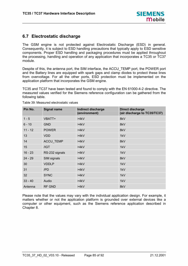
TC35 / TC37 Hardware Interface Description
TC35_37_HD_02_V03.10 - Released Page 85 of 92 21.12.2001
6.7 Electrostatic discharge
The GSM engine is not protected against Electrostatic Discharge (ESD) in general.Consequently, it is subject to ESD handling precautions that typically apply to ESD sensitivecomponents. Proper ESD handling and packaging procedures must be applied throughoutthe processing, handling and operation of any application that incorporates a TC35 or TC37module.
Despite of this, the antenna port, the SIM interface, the ACCU_TEMP port, the POWER portand the Battery lines are equipped with spark gaps and clamp diodes to protect these linesfrom overvoltage. For all the other ports, ESD protection must be implemented on theapplication platform that incorporates the GSM engine.
TC35 and TC37 have been tested and found to comply with the EN 61000-4-2 directive. Themeasured values verified for the Siemens reference configuration can be gathered from thefollowing table.Table 39: Measured electrostatic values
Pin No. Signal name Indirect discharge(environment)
Direct discharge(air discharge to TC35/TC37)
1 - 5 VBATT+ >4kV 8kV
6 - 10 GND >4kV 8kV
11 - 12 POWER >4kV 8kV
13 VDD >4kV 1kV
14 ACCU_TEMP >4kV 8kV
15 /IGT >4kV 1kV
16 - 23 RS-232 signals >4kV 1kV
24 - 29 SIM signals >4kV 8kV
30 VDDLP >4kV 1kV
31 /PD >4kV 1kV
32 SYNC >4kV 1kV
33 - 40 Audio >4kV 1kV
Antenna RF GND >4kV 8kV
Please note that the values may vary with the individual application design. For example, itmatters whether or not the application platform is grounded over external devices like acomputer or other equipment, such as the Siemens reference application described inChapter 8.

TC35 / TC37 Hardware Interface Description
TC35_37_HD_02_V03.10 - Released Page 86 of 92 21.12.2001
7 Updating FirmwareThe TC35 firmware is stored in a Flash memory. This gives you the flexibility to easilyupgrade to the latest firmware releases. The firmware is supplied as a Windows executablethat can be downloaded onto the GSM engine using the serial interface of its ZIF connectoror the SIM interface.
To meet the requirements of various application platforms there are a number of ways toperform the update. This chapter summarizes the options currently available. For detailedinformation, step-by-step instructions and possibly implied modifications to the hardwaredesign please refer to the "Firmware Updating User's Guide", /3/.
Updating the firmware over the serial interface• The download procedure uses the TXD0, RXD0 and IGT lines of the ZIF connector and
the TXD, RXD and DTR lines of the host application (MMI) or the PC's serial port. Theapproach to set up the serial link depends very much on the individual design of the hostapplication. The "Firmware Updating User's Guide" recommends the following methods:1. Download over DSB35 Support Box (evaluation kit).2. Download over service interface and service connector with the download being
supported by firmware executable.3. Download controlled by the processor of the host application (MMI processor).
Updating the firmware over the SIM interface• This solution is recommended when your GSM application has no direct access to a
serial interface. To transfer the software to the device you will need the BB35 Bootbox. Itcomes with a specific adapter that connects the SIM card reader of your TC35application to your computer's serial port.
In either case, the firmware executable runs on any computer under Windows 98, WindowsNT 4.0, Windows 2000, Windows ME, Windows XP (except for Windows 95 which supportsonly the serial interface option).

TC35 / TC37 Hardware Interface Description
TC35_37_HD_02_V03.10 - Released Page 87 of 92 21.12.2001
8 Reference Approval
8.1 Reference Equipment
The Siemens TC35 and TC37 GSM engines have been approved for referenceconfigurations that satisfy all the requirements of GSM Phase 2/2+ (CTR 31, CTR 32).
GSM enginePC
Power supply
SIM
FFC
RS232
DAI Box
DSB35
Handset
Acoustic tester
Antenna or 50Ohm cable tosystem simulator
GSC
DAI cable foracoustic measuring
Figure 45: Reference equipment for approval
Referred to as "GSM terminal equipment" the reference configuration consists of thefollowing components:- Siemens TC35 or TC37 cellular engine- Development Support Box (DSB)- SIM card reader integrated on the DSB- Handset type Votronic HH-SI-30.3/V1.1/0- PC as MMI
For the Siemens TC35 and TC37, an IMEI number contingent has been reserved for thebasic approval of the reference configuration. It will also apply to later approvals of customerconfigurations incorporating TC35 or TC37.
Approved Siemens TC35 and TC37 configurations are recorded in the approvaldocumentation. Later enhancements and modifications beyond the certified configurationrequire extra approvals. Each supplementary approval process includes submittal of thetechnical documentation as well as testing of the changes made. The relevant testapplications for supplementary approvals should be agreed upon with Siemens.

TC35 / TC37 Hardware Interface Description
TC35_37_HD_02_V03.10 - Released Page 88 of 92 21.12.2001
8.2 CE Conformity
TC35 and TC37 meet the requirements of EU directives listed below and is labeled with theCE conformity mark.- R&TTE Directive 1999/5/EG- LVD 73/23/EEC- EMC conformity in accordance with Directive 89/336/EEC
8.3 G.C.F. Conformity
TC35 and TC37 have been approved to comply with the quality assurance requirementsaccording to GCF-CCV and CCR, v. 3.4.1

TC35 / TC37 Hardware Interface Description
TC35_37_HD_02_V03.10 - Released Page 89 of 92 21.12.2001
9 APPENDIX: List of parts and accessories
Table 40: List of accessories
Description Supplier Ordering information
TC35 engine Siemens Siemens ordering numberL36880-N8100-A100
TC37 engine Siemens Siemens ordering number
L36880-N8150-A200
SIM card holder incl. push buttonejector and slide-in tray
Molex Ordering numbers: 9122891236
Molex Deutschland GmbHFelix-Wankel-Str. 11D-74078 Heilbronn-BiberachPhone: +49(7066)9555 0Fax: +49(7066)9555 29Email: [email protected] site: http://www.molex.com/
American HeadquartersLisle, Illinois 60532 U.S.A.Phone: 1-800-78MOLEXFax: 630-969-1352
Far East HeadquartersYamato, Kanagawa, JapanPhone: 81-462-65-2324Fax: 81-462
Far East HeadquartersJurong, SingaporePhone: 65-268-6868Fax: 65-265-6044
ZIF connector AVX Ordering number: 04 6240 040 003 800
Flat cable for ZIF connectorcable 160 mmcable 80 mm
Axon Ordering numbers:FFC 0.50 A 40 / 0160 K4.0-4.0-08.0-08.0SABBFFC 0.50 A 40 / 0080 K4.0-4.0-08.0-08.0SABB
RF cable GSC-GSCcable 50 mmcable 100 mm
MuRata Ordering numbers:MXTK 88 TK 0500MXTK 88 TK 1000
GSC connector MuRata MM9329-2700 TB2
P/N M22001 tool (recommendedfor GSC antenna installation)
MuRata Please use product name:P/N M22001
TC35 / TC37 Hardware Interface Description
TC35_37_HD_02_V03.10 - Released Page 90 of 92 21.12.2001
Description Supplier Ordering information
Coaxicon switching connector(TC37 only)
AMP /TycoElectronics
619028-1
Battery cell P/N"CGP34506 Panasonic"
ShenzhenXWODAelectronicCo., Ltd
To place orders or obtain more information pleasecontact:Mr. Wang Ming WangPhone: +86 755 7619731Fax: +86 755 7608078Email: [email protected]
Handset Votronic HH-SI-30.3/V1.1/0
Siemens Car Kit Portable Siemens Siemens ordering number
L36880-N3015-A117
DSB35 Support Box Siemens Siemens ordering number
L36880-N8101-A100-3
BB35 Bootbox Siemens Siemens ordering number
L36880-N8102-A100-1
9.1 Specifications of AMP switching connector
The following drawings are provided to help you select matching accessories for use with theAMP switching connector on TC37. For more details please visit the AMP Tyco homepagehttp://www.amp.com/ or contact your local dealer.

TC35 / TC37 Hardware Interface Description Ordering information for special accessories
TC35_37_HD_02_V03.10 - Released Page 91 of 92 21.12.2001
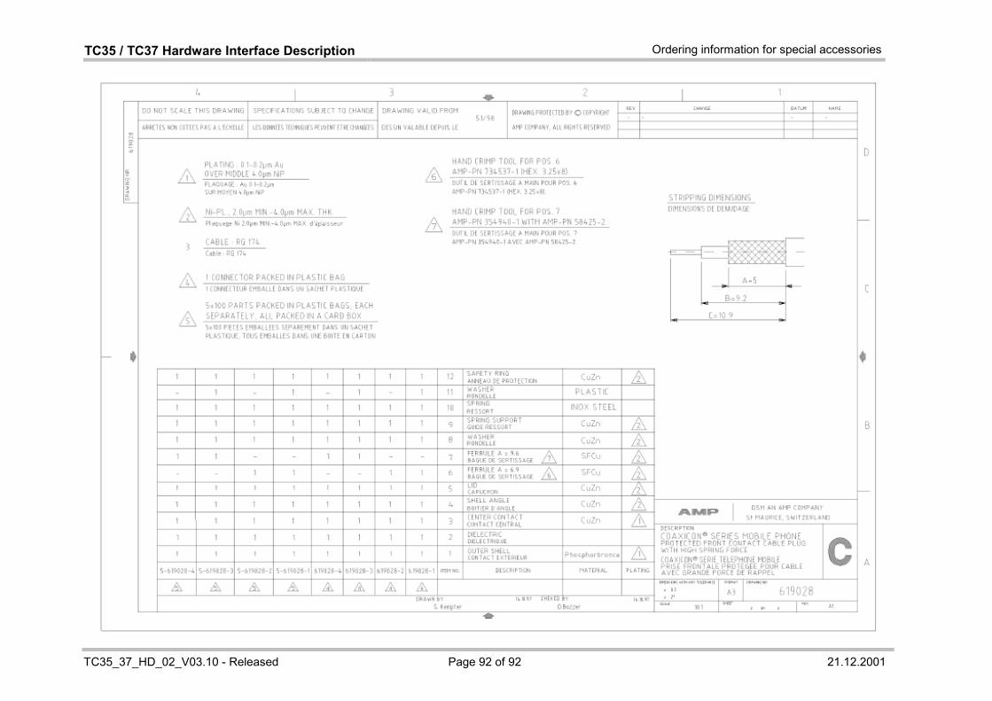
TC35 / TC37 Hardware Interface Description Ordering information for special accessories
TC35_37_HD_02_V03.10 - Released Page 92 of 92 21.12.2001