> positive, o> negative edge-triggered
TRANSCRIPT

Sequential Circuit Design
combinational circuit: each output depends entirely on the immediate (present) inputssequential circuit: each output depends on both present inputs and state ! Synchronous: outputs change only at specific time ! Asynchronous: outputs change at any time Multivibrator: a class of sequential circuits § Bistable (2 stable states) ! Latches and flip-flops. ! differ in the methods used for changing state. § Monostable or one-shot (1 stable state) § Astable (no stable state) Memory element: a device which can remember value indefinitely, or change value on command from its inputs. Two types of triggering/activation ! Level/Pulse-triggered § Latches § ON = 1, OFF = 0! Edge-triggered § Flip-flops § Positive edge-triggered (ON = 0 to 1; OFF = other time) § Negative edge-triggered (ON = 1 to 0; OFF = other time)
X+X⋅Y=XX+X’⋅Y=X+Y
X⋅Y+X⋅Z+Y⋅Z=X⋅Y+X’⋅ZY’⋅Z' + Y⋅Z=(Y⊕Z)'
Y'⋅Z + Y⋅Z’=Y⊕ZX+Y=(X⊕Y)+X⋅Y
Precedence from highest to lowest: Not (') And (⋅) Or (+) minterm - product term - SOP - find 1maxterm - sum term - POS - find 0Each minterm is the complement of the maxterm SOP - 2-level AND-OR/NAND circuitPOS - 2-level OR-AND/NOR circuitPLAs may not be able to implement a given mapping due to not having enough minterms. Half Adder: C = X∙Y, S = X'∙Y + X∙Y’ = X ⊕ YK-Maps -> SOPGate-Level (SSI) Design: Full-Adder, Code ConverterC = X⋅Y + (X⊕Y)⋅Z, S = X⊕(Y⊕Z) Block-Level Design: block: 4-bit parallel/ripple-carry adder: Ci+1 = Xi ⋅Yi + (Xi ⊕Yi)⋅Ci, Si =Xi ⊕Yi ⊕ Ci
Given a logic gate with delay t. If inputs are stable at times t1, t2, ..., tn, then the earliest time in which the output will be stable is: max( t1,t2,...,tn ) + t
1 KB= 210 bytes;
1 MB = 220 bytes;
1 GB = 230 bytes;
1 TB= 240 bytes.
Flip-Flops: synchronous bistable • Output changes state at a specified
point on a triggering input called the clock.
• Change state either at the positive (rising) edge, or at the negative (falling) edge of the clock signal.
Note “>” symbol at the clock input. > positive, o> negative edge-triggered
S-R flip-flop: On the triggering edge of the clock pulse positive edge-triggered S-R flip-flop
D flip-flop: On the triggering edge of the clock pulse
J-K flip-flop: Q and Q' are fed back to the pulse-steering NAND gates.
S-R Latch: Q(t+1)=S+R’•Q, S•R=0
Active-High
Active-Low
Gated D Latch: Q(t+1)=D
T flip-flop: Single input version of the J-K flip-flop Q(t+1)=T•Q’+T’•Q

encoder: exactly one input line is high and the rest are low, D0 =F1+F3, D1 =F2+F3
priority encoder: • If two or more inputs or equal to 1, the input with the
highest priority takes precedence.• If all inputs are 0, this input combination is considered
invalid.
demultiplexers: Given an input line and a set of selection lines, a demultiplexer directs data from the input to one selected output line. demultiplexer circuit is actually identical to a decoder with enable.
decoder: Convert binary information from n input lines to (a maximum of) 2n
output lines.
• Known as n-to-m-line decoder, or simply n:m or n x m decoder (m ≤ 2n).
• May be used to generate 2n minterms of n input variables.
SOP = decoder to generate minterms + OR gate to form the sumenable control signal: the device is only activated when the enable E = 1(one-enable) (MSI is mainly 0-enable)
multiplexer: It steers one of 2n inputs to a single output
line, using n selection lines. Also known as a data selector. • A number of input lines• A number of selection lines• One output line! Output of multiplexer is “sum of the (product of data lines and selection lines)” ! Example: Output of a 4-to-1 multiplexer is: Y = I0·(S1'·S0') + I1·(S1'·S0) + I2·(S1·S0') + I3·(S1·S0) = I0·m0 + I1·m1 + I2·m2 + I3·m3
A 2n-to-1-line multiplexer, or simply 2n:1 MUX, is made from an n:2n
decoder by adding to it 2n
input lines, one to
each AND gate.

§ IF: Instruction Fetch§ ID: Instruction Decode and Register Read§ EX: Execute an operation or calculate an address§ MEM: Access an operand in data memory§ WB: Write back the result into a register
Single Cycle§ Cycle time: § CTseq =∑k=1NTk § Tk = Time for operation in stage k§ N = Number of stages § Total Execution Time for I instructions:
Multi Cycle§ Cycle time: § CTmulti =max(Tk)§ max(Tk) = longest stage duration among the N stages § Total Execution Time for I instructions: § Timemulti = Cycles × CycleTime = I×Average CPI×CTmulti§ Average CPI is needed because each instruction takes different number of cycles to finish Pipeline Cycle§ Cycle time: § CTpipeline = max(Tk) + Td§ max(Tk) = longest time among the N stages § Td = Overhead for pipelining, e.g. pipeline register § Cycles needed for I instructions: § I + N -1§ N - 1 is the cycles wasted in filling up the pipeline § Total Execution Time for I instructions: § Timepipeline = Cycle × CTpipeline = (I + N -1) × (max(Tk) +
Ideal Speedup• Every stage takes the same amount of time• No pipeline overhead Td=0• Number of instructions I is much larger than number of
stages NSpeeduppipeline = Timeseq / TimepipelinePipeline processor can gain N times speedup, where N is the number of pipeline stages
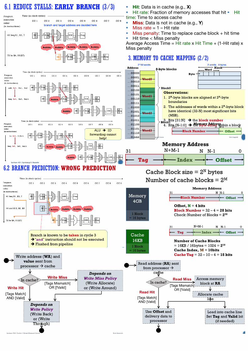
! Hit: Data is in cache (e.g., X)! Hit rate: Fraction of memory accesses that hit ! Hit time: Time to access cache ! Miss: Data is not in cache (e.g., Y)! Miss rate = 1 – Hit rate! Miss penalty: Time to replace cache block + hit time ! Hit time < Miss penaltyAverage Access Time = Hit rate x Hit Time + (1-Hit rate) x Miss penalty

! Two types of RAM ! Static RAMs use flip-flops as the memory cells. ! Dynamic RAMs use capacitor charges to represent data. Though simpler in circuitry, they have to be constantly refreshed.