guidelines for accelerated reliability testing of surface
TRANSCRIPT

IPC-SM-785
Guidelines for Accelerated
Reliability Testing of Surface
Mount Solder Attachments
ASSOCIATION CONNECTINGELECTRONICS INDUSTRIES
2215 Sanders Road, Northbrook, IL 60062-6135Tel. 847.509.9700 Fax 847.509.9798
www.ipc.org
IPC-SM-785November 1992 A guideline developed by IPC

The Principles ofStandardization
In May 1995 the IPC’s Technical Activities Executive Committee adopted Principles ofStandardization as a guiding principle of IPC’s standardization efforts.
Standards Should:• Show relationship to Design for Manufacturability
(DFM) and Design for the Environment (DFE)• Minimize time to market• Contain simple (simplified) language• Just include spec information• Focus on end product performance• Include a feedback system on use and
problems for future improvement
Standards Should Not:• Inhibit innovation• Increase time-to-market• Keep people out• Increase cycle time• Tell you how to make something• Contain anything that cannot
be defended with data
Notice IPC Standards and Publications are designed to serve the public interest through eliminatingmisunderstandings between manufacturers and purchasers, facilitating interchangeability andimprovement of products, and assisting the purchaser in selecting and obtaining with minimumdelay the proper product for his particular need. Existence of such Standards and Publicationsshall not in any respect preclude any member or nonmember of IPC from manufacturing or sell-ing products not conforming to such Standards and Publication, nor shall the existence of suchStandards and Publications preclude their voluntary use by those other than IPC members,whether the standard is to be used either domestically or internationally.
Recommended Standards and Publications are adopted by IPC without regard to whether theiradoption may involve patents on articles, materials, or processes. By such action, IPC doesnot assume any liability to any patent owner, nor do they assume any obligation whatever toparties adopting the Recommended Standard or Publication. Users are also wholly responsiblefor protecting themselves against all claims of liabilities for patent infringement.
IPC PositionStatement onSpecificationRevision Change
It is the position of IPC’s Technical Activities Executive Committee (TAEC) that the use andimplementation of IPC publications is voluntary and is part of a relationship entered into bycustomer and supplier. When an IPC standard/guideline is updated and a new revision is pub-lished, it is the opinion of the TAEC that the use of the new revision as part of an existingrelationship is not automatic unless required by the contract. The TAEC recommends the useof the lastest revision. Adopted October 6. 1998
Why is therea charge forthis standard?
Your purchase of this document contributes to the ongoing development of new and updatedindustry standards. Standards allow manufacturers, customers, and suppliers to understand oneanother better. Standards allow manufacturers greater efficiencies when they can set up theirprocesses to meet industry standards, allowing them to offer their customers lower costs.
IPC spends hundreds of thousands of dollars annually to support IPC’s volunteers in thestandards development process. There are many rounds of drafts sent out for review andthe committees spend hundreds of hours in review and development. IPC’s staff attends andparticipates in committee activities, typesets and circulates document drafts, and follows allnecessary procedures to qualify for ANSI approval.
IPC’s membership dues have been kept low in order to allow as many companies as possibleto participate. Therefore, the standards revenue is necessary to complement dues revenue. Theprice schedule offers a 50% discount to IPC members. If your company buys IPC standards,why not take advantage of this and the many other benefits of IPC membership as well? Formore information on membership in IPC, please visit www.ipc.org or call 847/790-5372.
Thank you for your continued support.
©Copyright 1992. IPC, Northbrook, Illinois. All rights reserved under both international and Pan-American copyright conventions. Anycopying, scanning or other reproduction of these materials without the prior written consent of the copyright holder is strictly prohibited andconstitutes infringement under the Copyright Law of the United States.

IPC-SM-785
Guidelines for Accelerated
Reliability Testing of
Surface Mount Solder
Attachments
Developed by the SMT Accelerated Reliability Test Task Group of theProduct Reliability Committee of IPC
Users of this standard are encouraged to participate in thedevelopment of future revisions.
Contact:
IPC2215 Sanders RoadNorthbrook, Illinois60062-6135Tel 847 509.9700Fax 847 509.9798
ASSOCIATION CONNECTINGELECTRONICS INDUSTRIES

AcknowledgmentAny Standard involving a complex technology draws material from a vast number of sources. While the principal membersof the SMT Accelerated Reliability Test Task Group of the IPC Product Reliability Committee are shown below, it is notpossible to include all of those who assisted in the evolution of this standard. To each of them, the members of the IPCextend their gratitude.
Product ReliabilityCommittee
SMT Accelerated ReliabilityTest Task Group
Technical Liaison of theIPC Board of Directors
ChairmanWerner EngelmaierEngelmaier Associates, Inc.
ChairmanWerner EngelmaierEngelmaier Associates, Inc.
Patrick SweeneyHadco
SMT Accelerated Reliability Test Task Group
P. J. Amick, McDonnell DouglasElec. Sys. Co.
E.M. Aoki, Hewlett-PackardLaboratories
J. Appelbaum, Wang Labs
F.E. Bader, AT&T Bell Labs
D.B. Barker, University of Maryland
A. Beikmohamadi, EI DuPont DeNemours & Co.
F. Bellia, Raytheon Co.
M.G. Bevan, Johns HopkinsUniversity
P. Borela, Jet Propulsion Lab
C. Bradshaw, Memorex Telex Corp.
V.J. Brzozowski, WestinghouseElectric Corp.
J.S. Burg, 3M Co.
L.W. Canarr, Rockwell International
T.A. Caroll, Hughes Aircraft Co.
A. Cash, Northrop Corp.
H.B. Collins, AMP Inc.
S.J. Croce, Litton Aero Products Div.
D. Currier, Ambitech Inc.
A. Dasgupta, University of Maryland
J.A. DeVore, General Electric Co.
M.J. DiFranza, Mitre Corp.
W.C. Dieffenbacher, General ElectricCo.
B. Dilden, Siemens IndustrialAutomation
J.L. Donahoe, General Electric Co.
R.S. Druckenmiller, AMP Inc.
R. Elias, Motorola Inc.
W. Engelmaier, EngelmaierAssociates, Inc.
M.J. Engler, Hughes Aircraft Co.
J.W. Evans, NASA HQ
E. Francischelli, Litton SystemsInc./Amecom Div.
M.S. Gandhi, Hughes Aircraft Co.
V. Gandhi, Teradyne ConnectionsSystems
C. Gonzalez, SCI Manufacturing Inc.
G.A. Gorsche, Litton SystemsInc./Amecom Div.
F. Gray, Texas Instruments Inc.
C. Grosskopf, IBM Corp.
B. Gulati, Parker/Gull Electronic Sys.Div.
W.B. Hampshire, Tin Information Ctr.of N. America
L. Harford, Texas Instruments Inc.
M.E. Hill, Digital Equipment Corp.
D.D. Hillman, Rockwell International
M. Hook, U.S. Navy
L. Hymes, Plexus Corp.
A. Jang, Litton Systems Canada Ltd.
N. Joglekar, Digital Equipment Corp.
K.L. Johnson, Hexacon Electric Co.
T. Jones, U.S. Navy
G.W. Kenealey, Control Data Corp.
J.L. Kessler, Litton Systems Inc./Amecom Div.
T. Kocher, AMP Inc.
D. Kopp, Johns Hopkins University
F. Kreis, NASA/Goddard SpaceFlight Cntr.
G.K. Krieg, TRW
V. Kumar, Martin-MariettaElectronics
L.P. Lambert, Digital EquipmentCorp.
N. Le, Quynhgiao, Boeing Aerospace& Electronics
A. Lee, Hewlett-Packard Co.
W. Lewis, Kaiser Electronics
G. Lovati, Alcatel Italia S.P.A.
J.F. MaGuire, Boeing Aerospace &Electronics
J.R. Maki, Harris Corp.
H.A.J. Mann, Litton SystemsInc./Amecom Div.
J.M. Mc Creary, IBM Corp.
J. H. Moffitt, U.S. Navy
K. Mulholland, Paramax SystemsCorp.
G.C. Munie, AT&T Bell Laboratories
E. Nicewarner, Fairchild/SpaceCompany
D. Noctor , AT&T Bell Labs
D.T. Novick, Rockwell International
T. Ohman, Ericsson Telecom
G. Oleynick, EI DuPont De Nemours& Co.
W. Olssen, Lockheed EngineeringAnd
A.G. Osborne, Alliant TechsystemsInc.
R. Payne, Sundstrand Data ControlInc.
D.O. Pond, U.S. Navy
C. Ramirez, Compaq Computer Corp.
M. Reithinger, Siemens AG
J.A. Root, Martin-Marietta Corp.
J.G. Rosser, Hughes Aircraft Co.
D. Rudy, AT&T Bell Laboratories
D.W. Rumps, AT&T TechnologySystems
IPC-SM-785 November 1992
ii

D.C. Sandkulla, Hughes Aircraft Co.
M. Saum, Lockheed Sanders
R. Savage, NASA/GoddardspaceFlight Cntr.
D. Schoenthaler, AT&T BellLaboratories
R.L. Sellers, U.S. Navy
W. Sepp, Learonal Inc.
N. Socolowski, Alpha Metals
V. Solberg, SCI Systems
P.S. Speicher, U.S. Air Force
L.G. Svendsen, Elf Technologies
D. Swenson, Bendix/King Atad
R.T. Thompson, Loctite Corp.
J.S. Tucker, Unisys Corp.
L.J. Turbini, Georgia Institute/Technology
H. Underwood, U.S. Air Force
R. Van Buskirk, Wang Labs
N. Virmani, Paramax Systems Corp.
D.L. Wasler, Jet Propulsion Lab
S. Witzman, Northern Telecom Ltd.
J.R. Wooldridge, RockwellInternational
November 1992 IPC-SM-785
iii

Table of Contents
1.0 SCOPE .................................................................... 1
1.1 Purpose................................................................. 1
1.2 Document Organization ....................................... 1
2.0 APPLICABLE DOCUMENTS ................................... 2
2.1 IPC........................................................................ 2
2.2 Joint Industry Standards ...................................... 2
2.3 Military................................................................. 2
2.4 Other Publications................................................ 2
3.0 REQUIREMENTS
3.1 Terms and Definitions.......................................... 3
3.2 Reliability Concepts and Understanding............. 5
3.3 Reliability Assurance ........................................... 6
3.4 Damage/Failure Mechanisms ............................ 10
3.5 Application Considerations................................ 12
4.0 SURFACE MOUNT SOLDER ATTACHMENTFATIGUE BEHAVIOR AND RELIABILITYPREDICTION ......................................................... 15
4.1 General Fatigue Life Models ............................ 15
4.2 Solder Joint Fatigue........................................... 15
4.3 Fatigue Behavior of Solder Joints..................... 16
4.4 Acceleration Factors/AccelerationTransform........................................................... 19
4.5 Statistical Considerations................................... 20
5.0 DESIGN FOR SOLDER ATTACHMENTRELIABILITY ......................................................... 22
5.1 Primary Design Parameters ............................... 22
5.2 Secondary Design Parameters ........................... 23
6.0 MANUFACTURE/PROCESSES ............................. 24
6.1 Process Control and Verification ....................... 24
6.2 Consequences of Defects................................... 24
6.3 Material Properties............................................. 27
7.0 ACCELERATED RELIABILITY TESTING
7.1 Reliability Program/Strategy ............................. 30
7.2 Generic Damage Mechanism Investigations..... 30
7.3 Thermal Cycling ................................................ 30
7.4 Mechanical Cycling ........................................... 32
7.5 Vibration............................................................. 32
7.6 Creep Rupture Tests........................................... 33
7.7 Mechanical Shock Testing................................. 34
7.8 Failure Criteria for Solder JointFatigue Tests ...................................................... 34
7.9 Accelerated Life Test Planning ......................... 35
7.10 Failure Mode Analysis....................................... 38
7.11 Reporting Results............................................... 41
Appendix A Step-by-Step Example ........................... 43
Appendix B References .............................................. 45
Appendix C Bibliography ........................................... 46
Figures
Figure 1 Flowchart for reliability....................................... 4
Figure 2 Generic reliability ‘‘bathtub’’ curves comparingelectronic components and surface mountsolder attachment .............................................. 6
Figure 3 Generic cumulative failure probabilities forelectronic component and surface mountsolder attachment .............................................. 7
Figure 4 Flow chart for surface mount solderattachment reliability assurance ........................ 8
Figure 5 Cumulative fatigue damage............................. 10
Figure 6 SMT assembly thermo-mechanicaldeflections resulting from thermal gradientsin thermal shock .............................................. 13
Figure 7 Thermal cycle/fatigue mechanismsfor solder.......................................................... 18
Figure 8 Shear strengths of 60:40 SnPb solder asa function of temperature and strain rate........ 28
Figure 9 Creep behavior of solder ................................. 34
Figure 10 Example of circuit layout ................................. 36
Figure 11 Internal lead connection schemes forodd lead numbers per side.............................. 37
Tables
Table 1 Worst-Case Use Environments for SurfaceMounted Electronics and RecommendedAccelerated Testing ............................................ 14
Table 2 Equivalent Mean Accelerated Test Cycles......... 21
Table 3 Typical Values .................................................... 29
Table 4 Properties of Printed Board Laminates.............. 31
Table 1A Results of Accelerated Reliability Test ............... 43
IPC-SM-785 November 1992
iv

September 1992 IPC-SM-785
Guidelines for Accelerated Reliability Testingof Surface Mount Solder Attachments
il-fortec-is
es
t-hetindeel-
-
heat
n
ery
esofail-
one
erv.er
li-n-reric-th
e
erle
ghareand
hatueeef-sluee
em-ndctsair),
malandfac-
toestoer-edd isestre
s.
la-
onr-re
ede
1.0 SCOPE
This document provides guidelines for accelerated reliabity testing of surface mount solder attachments andevaluating and extrapolating the results of these accelerareliability tests towards actual use environments of eletronic assemblies. Background and design informationprovided for an understanding of the accelerated tissues.
1.1 Purpose The purpose of accelerated reliability tesing is to provide confidence that the design and tmanufacturing/assembly processes are capable of meethe intended goals of product performance. These guilines provide adequate commonality and validity for accerated reliability tests:
• To allow comparison of results from different test programs
• To provide the generic technical understanding of tunderlying issues necessary to the design for adequreliability
• To permit the analytical prediction of reliability based oa generic database and technical understanding
• To reduce cost and avoid time-consuming testing of evdesign iteration
• To establish practical alternatives to replace the excsively long test durations necessary to verify reliabilityproducts subject to severe use environments or low fure tolerances
1.2 Document Organization This document has beenorganized to provide the reader with consistent information the various aspects of reliability and identifies thparameters that need to be addressed. Each section sa specific function in the reliability description chainWhere appropriate, references are provided as to whadditional information may be obtained.
• Section 3, ‘‘Requirements’’This section provides an overview of the concepts of reability and all of the characteristics that need to be cosidered in the validation of a product design. Included athe definitions of the appropriate terms, as well as genemodels for fatigue life and failure probability, manufacturing process flow, use environments, and testing meodology.
• Section 4, ‘‘Surface Mount Solder Attachment FatiguBehavior and Prediction’’This section deals with the fatigue life models for soldjoints including their behavior when subjected to multip
d
t
g-
e
-
es
e
-
cyclic loads during large temperature excursions or hifrequency cycles at low temperatures. Also discussedthe acceleration factors, the acceleration transforms,statistical considerations.
• Section 5, ‘‘Design for Solder Joint Reliability’’This section details the various design parameters thave a primary influence on solder attachment fatigreliability. All aspects of the solder joint formation araddressed including component size, lead stiffness, coficient of thermal expansion, solder joint uniformity, awell as solder composition, grain structure and the vathat conformal coating or compliant layers provide to thattachment system.
• Section 6, ‘‘Manufacturing Processes’’This section provides the relationship between the assbly and attachment processes, including their control averification, and the resultant defects or potential defefrom the original processes or touch-up, rework or repactions. Material properties of solder (including volumecomponents, printed boards, adhesives and conforcoatings are discussed as to their interrelationshipsthe impact that these characteristics have on the manuturing processes.
• Section 7, ‘‘Accelerated Reliability Testing’’This section deals with the goals of accelerated testingproduce a failure in the shortest time using techniquintended to simulate the use environment in orderestablish the appropriate confidence level of product pformance. Various types of stress cycling are reviewand correlated to damage mechanisms. Also discussethe need for developing a strategy which includes a tplan, sampling methodology, test vehicles, and failumode analysis.
• Appendix A, ‘‘Step-by-Step Example’’This section shows illustrations of applying the principledetailed in the information provided in this publicationNumerical examples are provided that highlight the retionship of the various parameters.
• Appendix B, ‘‘References’’This section provides reference to published informatithat has a bearing on solder joint reliability and is refeenced in the body of the text of this document. Details ashown as to Title, Author, and Publisher.
• Appendix C, ‘‘Bibliography’’This section provides references to additional publishinformation that could be of use to the practitioner. Threferences are organized into three major topics
1

ct,ed
d
of
al
,
s
of
c-
r-
t-
esasl-i-lyt
n--
se
rensy
Itedke
ng-
n-lm
yanr-
to
b-
itdli-
on-e
IPC-SM-785 September 1992
1) Accelerated Life Testing
2) Solder Joint Metallurgy and Etching
3) Vibration and Shock.
2.0 APPLICABLE DOCUMENTS
The following documents, of the issue currently in effeform a part of this specification to the extent specifiherein.
2.1 IPC1
IPC-T-50 Terms and Definitions for Interconnecting anPackaging Electronic Circuits
IPC-PC-90 General Requirements for ImplementationStatistical Process Control
IPC-TM-650 Test Methods Manual
IPC-ET-652 Guidelines and Requirements for ElectricTesting of Unpopulated Printed Boards
IPC-R-700 Suggested Guidelines for ModificationRework, and Repair of Printed Boards and Assemblies
IPC-TA-720 Technology Assessment of Laminates
IPC-SM-782 Surface Mount Land Patterns (Configurationand Design Rules)
IPC-SM-786 Recommended Procedures for HandlingMoisture Sensitive Plastic IC Packages
IPC-MS-810 Guidelines for High Volume Microsection
IPC-S-816 SMT Process Guideline & Checklist
2.2 Joint Industry Standards1
J-STD-001 Requirements for Soldered Electrical and Eletronic Assemblies
J-STD-002 Solderability Tests for Component Leads, Teminations, Lugs, Terminals and Wires
J-STD-003 Solderability Tests for Printed Boards
2.3 Military
MIL-HDBK-217
MIL-STD-810
2.4 Other Publications
American Society for Testing and Materials
ASTM E340-68 Standard Methods for Macroetching Meals and Alloys
2
ASTM E407-70 Standard Methods for Microetching Metaland Alloys
International Tin Research Institute
ITRI Pub #580 Metallography of Tin and Tin Alloys
ITRI Pub #708 Metallurgy of Solder Joints in Electronics
3.0 REQUIREMENTS
The reliability of the solder joint attachment of electroniccomponents surface mounted to circuit board substratrequires explicit attention in the design phase, as wellduring manufacturing. During use, surface mount (SM) soder joints can be subjected to a variety of loading condtions which can lead to premature failure if inadequatedesigned. The following loading conditions could exiseither singly, sequentially or simultaneously:
a) cyclic differential thermal expansion,
b) vibration (transport),
c) thermal shock (rapid temperature change causing trasient differential warpages) during cooling from soldering operation or from severe use environments,
d) mechanical shock (high acceleration) from severe uconditions or accidental misuse.
While vibration, thermal shock and mechanical shock apossible in practical applications, they are the exceptiorather than the norm; the failure mechanism of primarconcern for SM solder joint reliability is cyclic differentialthermal expansion/contraction causing fatigue damage.should be noted that the resistance against failures inducby vibration fatigue, thermal shock and mechanical shocdepends primarily on solder joint strength; this is not thcase, however, for thermal fatigue failure resistance.
These thermal expansion differences result from changitemperatures due to power dissipation internal to the component and differences in the coefficients of thermal expasion (CTE) in combination with system internal or externatemperature variations caused by component or systeload fluctuations or on/off cycles, by diurnal cycles, or bseasonal changes. During operation, SM solder joints cbe subjected to considerable cyclic strains caused by diffeent thermal expansions of:
1. The surface mounted components and the substrateswhich they are solder-attached.
2. The solder and the materials (component, lead, sustrate) to which it is bonded.
To ascertain that the solder joint attachment of SM circuassemblies meet reliability expectations in their intendeuse environments, it is necessary to produce a generic reability data base using accelerated fatigue tests and to cfirm the reliability for some specific applications. Becaus
1. Publications are available from IPC, 2215 Sanders Road, Northbrook, IL 60062-6135

tirraedhr-eth
er
erihba
h
eb
n
tileer
-
s
oin
ere
to
edf anentingsesnsingired,tureant
is
r-s
resan
mid-ndol-
nlevesis
a-b-
c-
ieda
ringal
September 1992 IPC-SM-785
of the time dependent creep and stress relaxation properof solder, the cyclic damage and the fatigue life in acceleated testing are not generally equivalent to those in opetional use. Thus, to utilize the results from acceleratfatigue tests, an acceleration transform is necessary. Tallows valid comparisons of results from different acceleated test conditions and more importantly, allows thextrapolation of these accelerated test results to predictreliability of the product in use.
3.1 Terms and Definitions Terms and definitions usedherein are in accordance with IPC-T-50, except as othwise specified.
Note: Any definition denoted with an asterisk (*) is areprint of the definitions in IPC-T-50.
3.1.1 Accelerated Reliability Test A test in which thedamage mechanism(s) of concern for operational use(are) accelerated to cause failures in less time than in svice. The test acceleration results from shorter cycle peods and/or more severe loading conditions; however, tintroduction of extraneous damage mechanisms mustavoided. The service life can be characterized by appliction of appropriate acceleration factors or transforms.
3.1.2 Acceptable Cumulative Failure Probability Maxi-mum percentage of defectives/failures at the end of tservice life within acceptable limit.
3.1.3 Bathtub Curve Methodology for quantifying reli-ability when the failure rate is plotted against time. Thresult often follows a pattern of failure known as a bathtucurve. Three periods are apparent. These periods differthe frequency of failure and in the failure causation patter
3.1.4 Burn-In Test A test in which finished product isroutinely subjected to normal, perhaps worst-case but srealistic, operational environments. In purpose it resembthe shakedown cruise of a ship. Burn-in is not an accelated reliability test.
3.1.5 Creep The time-dependent visco-plastic deformation as a function of applied stress.
3.1.6 Coffin-Manson Model A predictive model whichrelates the number of cycles to failure to the applied platic strain.
3.1.7 Cyclic Differential Expansion Expansion differ-ences developed due to the differences in coefficientsthermal expansion and cyclic temperature changes duroperational use or temperature cycling tests.
3.1.8 Cyclic Temperature Range/Swing Temperatureamplitude between maximum and minimum temperaturoccurring in operational service cycles or temperatucycling tests.
es--
is
e
-
isr--ee-
e
in.
lls-
-
fg
s
3.1.9 Design Service Life Fully functional duration ofoperation of a piece of equipment which is exposedexpected environment conditions.
3.1.10 Environmental Stress Screening (ESS) A screen-ing procedure employing environmentally generatstresses to cause overstressing of ‘weak’ elements oassembly to the point of failure to prevent these latdefects from reaching field service and possibly causfield failures. The environments producing these stresmay, or may not, be related to environmental conditioexperienced by the product during service. Once havfailed, the elements can be detected and either repareplaced, or discarded; and perhaps redesigned for fuproduct. ESS needs to be accomplished without significdamage to the ‘normal’ elements of the assembly. ESSnot an accelerated reliability test.
3.1.11 Expected Design Life Life intended for a productby its designer.
3.1.12 Fatigue Ductility Exponent Exponent used in theCoffin-Manson low-cycle fatigue model to define the chaacteristic slope of the curve defining cyclic life versucyclic visco-plastic strain energy.
3.1.13 Highly Accelerated Stress Testing (HAST) Astress test used to simulate corrosion related failumechanisms under electrical bias while subjected toaccelerated stress combination of temperature and huity. HAST may be used in the context of components aassemblies, but is not an accelerated reliability test for sder attachment.
3.1.14 Hysteresis Loop A diagram of the stress-straibehavior of solder joints obtained during a loading cycfrom zero to a positive maximum, to zero to a negatimaximum, and back to zero—the area of the hystereloop is a measure of the fatigue damage per cycle.
3.1.15 Infant Mortality Failure during burn-in, initialfunctional testing, and/or early in service associated primrily with manufacturing process or quality related prolems.
3.1.16 Limp Home Capability Ability of equipment tofunction at a minimum level despite limited internal funtional failures.
3.1.17 Manson-Coffin Plot A graphic representationwhich relates the number of cycles to failure to the applplastic strain for both plastic and elastic behavior ofmaterial.
3.1.18 Maximum Cyclic Strain Range The total strainrange experienced after complete stress relaxation duexposure to cyclically induced thermal or mechanicdeformations.
3

IPC-SM-785 September 1992
IPC-785-1
Figure 1 Flowchart for reliability
Determinemissing
data.
Isinformation
complete enoughfor reliability
analysis?
Section 3
Isreliability insection 4.3applicable?
Estimate productreliabilitySection 4
Redesign product.Redefine
requirements.
Isestimatedreliability
adequate?
Finish
Solution:RedesignRedefine
ReduceUncertainties
Solution:RedesignRedefine
Review testprogram forcorrect-ness
Finish
Isreliabilityadequate
?
Collection ofall available
information & requirements
Define propertest, conditions,details Section 7
Acceleratedreliability
test(s)
Evaluate resultsFailure Mode
Analysis
Estimate productreliability from
test results
Yes
No
Yes
Yes
No
No
Yes
No
Main Focus of Document
4

nten
a
ur
m
e
t.
eion
-m.
-ienle°C
si-
rehe
ofto
g
to
-
fe.,2
h-for-slifetheatetlyhent;thisl-
isallof
on-etc.n-eanig-
ls,ron-nn-i-e-er
ductt-e
llyreli-ult
September 1992 IPC-SM-785
3.1.19 Mean Fatigue Life The life at which one-half ofa given sample of items has failed.
3.1.20 Mechanical Shock A rapid transfer of mechani-cal energy to a system, which results in a significachange in stress, velocity, acceleration, or displacemwithin the system.
3.1.21 Process Qualification A special test(s) performedto validate a process capability in terms of producingproduct capable of meeting performance specifications.
3.1.22 Process Verification Ongoing evaluation of pro-cesses involved in the manufacturing of a product to assprocess optimization or to eliminate process deviations.
3.1.23 Random Steady State Period of useful opera-tional life during which failures occur seemingly at randoat a low rate weakly related to product complexity.
3.1.24 Reliability The ability of a product to functionunder given conditions and for a specified period of timwithout exceeding an acceptable failure level.
3.1.25 Solder Attachment The collection of solderjoints (solder connections) associated with a componen
3.1.26 Stress Relaxation The time-dependent decreasin stress due to the visco-plastic deformation as a functof applied displacement.
3.1.27 Thermal Cycling (See 3.4.1) Exposure of assemblies to cyclic temperature changes where the rate of teperature change is slow enough to avoid thermal shock
3.1.28 Thermal Shock (See 3.4.3) Exposure of assemblies to rapid changes of temperatures causing transtemperature gradients, warpages, and stresses. As a ruthumb, rates of temperature change in excess of 30minute are required.
3.1.29 Vibration A periodic, typically elastic, motion ofa structure in alternately opposite directions from the potion of equilibrium.
3.1.30 Visco-Plastic Strain Energy Density A measureof the total energy input into a cyclically loaded structudefined by the boundaries of a hysteresis loop for tapplied stress versus strain over a single load cycle.
3.1.31 Wearout The process where the occurrencesfailures rise steadily as the product deteriorates dueaccumulating (fatigue) damage.
t
e
-
tof/
3.1.32 Weibull Distribution A statistical description ofthe distribution of product failure primarily useful inwearout situations.
3.2 Reliability Concepts and Understanding In the con-text of this document it is important to have a workindefinition of reliability:
Reliability is the ability of a product (for this documentthe products are surface mount solder attachments)function under given conditions and for a specifiedperiod of time without exceeding acceptable failure levels.
Implicit in this definition is the fact that the reliability oSM solder joints is determined by wearout (fatigue), i.on a time-to-failure plot (the ‘‘bathtub curve’’). Figureshows individual ‘‘bathtub’’ reliability plots for SM solderattachments and for a ‘‘typical’’ electronic component witout the solder attachment. Figure 3 shows the same inmation in the form of cumulative failure probability plotfor the component and the SM solder attachment. Theof the solder attachment is primarily characterized byright ascending part of the curve, where the failure rrapidly increases with time due to wearout. This direcimplies that manufacturing quality cannot increase tinherent reliability of a design in a given use environmehowever, inadequate manufacturing quality can reduceinherent designed-in reliability by increasing infant mortaity failures.
Manufacturing introduces variability into the product. Thvariability encompasses ranges of all the properties forthe materials in the product, ranges in the dimensionsparts due to tolerance, compositional variations and nhomogeneities, fluctuations in processing parameters,In good quality manufacturing these variabilities are cotrolled within ranges that will not significantly degradproduct performance. Manufacturing of lesser quality cintroduce larger variabilities and/or defects, which can snificantly reduce product performance.
Superimposed on these product variabilities (materiaprocessing, etc.) are differences in the actual use enviment, as well as reliability (fatigue) distributions. Eveproduct that is nominally identical when subjected to idetical loading conditions will show a statistical failure distrbution. Since accelerated reliability testing is timconsuming and costly, it is typically carried out on a rathsmall number of samples. To capture representative provariabilities and their effect on reliability requires the tesing of a sufficiently large number of samples to includthese variables. The controlled introduction of artificiacreated defects that are assumed to have a significantability impact would serve the same purpose but is difficto achieve in practice.
5

IPC-SM-785 September 1992
IPC-785-2
Figure 2 Generic reliability ‘‘bathtub’’ curves comparing electronic components and surface mount solder attachment
101 102 103 104 105 1060.1
1
10
102
103
104
Operating Time [Hours]
Inst
anta
neou
s F
ailu
re R
ate
(FIT
s)
Electronic Component w/o Attachment
InfantMortality
SM SolderAttachment
Wearout
SteadyState
40 Years1
LeadlessLeaded
5
-’’dvese
theine
’’anhegeo-ndr
wit
at
r-ner,m
-ni-icte’’rn.
tsthem-
.
ases4
The reliability ‘‘bathtub’’ curves in Figure 2, as well as theresulting cumulative failure probability plots shown in Figure 3, need some explanation. The ‘‘infant mortality,‘‘random steady-state,’’ and ‘‘wearout’’ regions are defineby which of these three failure modes dominate. The curintersections in Figure 2 delineate the extent of theregions.
Except for the SM solder attachment wearout regions,values plotted are rather ‘‘soft.’’ Hard data does not existadequate quantities for either the component or soldattachment ‘‘infant mortality’’ and ‘‘random steady-stateregions. These plot regions are based on experienceobserved trends and some published information. T‘‘steady-state’’ region for components depends to a larextent on the complexity of the component; chip compnents would fail well below the indicated bathtub band avery complex, high I/O chip carriers would fail at higherates.
For SM solder attachment, no evidence exists that shothat the ‘‘random steady-state’’ failure region even exists;is entirely possible that ‘‘infant mortality’’ and ‘‘wearout’’form the entire failure rate history. It should be noted th
6
r
d
s
for SM solder attachments, the ‘‘infant mortality’’ and‘‘random steady-state’’ failure regions are rather unimpotant since the failure probabilities are very small eveassuming order of magnitude errors. Significant howevis the experience-based observation that the ‘‘randosteady-state’’ failure rate estimate given in MIL-HDBK217 is too high by perhaps two or three orders of magtude. Figures 2 and 3 imply that the reliability of electroncomponents is determined by the ‘‘random steady-stafailure region. In contrast, the reliability of the SM soldeattachment is established by the ‘‘wearout’’ failure regio
The cumulative failure probability of a component and iSM solder attachment is the sum of the component andattachment failure probabilities. Thus an electronic assebly is more likely to fail due to component failure in theshort-term and due to solder joint failure in the long-term
3.3 Reliability Assurance Surface mount solder jointreliability requires explicit attention in the design phasewell as in manufacturing. An overview of the processleading to reliability assurance is outlined in the Figureflow chart.

September 1992 IPC-SM-785
IPC-785-3
Figure 3 Generic cumulative failure probabilities for electronic component and surface mount solder attachment
101 102 103 104 105 106 107
0.01
0.1
1
10
50
99.9
0.001
0.0001
Operating Time [Hours]
40 Years
Cum
ulat
ive
Fai
lure
Pro
babi
lity
[%]
5
Electronic Componentw/o Attachment
SM SolderAttachment
Leadless
Leaded
1
-,ectovad
theve
enoucd.nicea. An o
esesststeseons,
ty’’nd
curms.ermuntheg-
ess-guelendessoste
ndue
for
ofn-orng
3.3.1 Generic Understanding of Solder Attachment
Technology Solder is unique due to its temperaturetime-, and stress-dependent behavior. For instance, euttin-lead solder readily creeps and stress relaxes ab20°C, whereas below –20°C solder has long-term lobearing capabilities similar to other metals. The highertemperature above 20°C and/or the higher the stress lethe faster the solder will creep and stress relax.
A generic understanding of the reliability and failurmechanisms for a given surface mount attachment techogy is the first step toward designing and assuring prodreliability. For this, a generic database is requireAlthough failure mechanisms based on cyclic or monotooverstressing can occur, the most common reliability thrcomes from stress-relaxation based fatigue damagefatigue failure database must be based on a combinatiolow acceleration and high acceleration tests.
In this context, low acceleration tests produce mean-timto- failure of the test vehicles that are about 10 to 20 timshorter than actual life in field use. High acceleration teare about 100 to 500 times shorter. The higher theacceleration, the less the test results are representativperformance at field conditions. Thus, low acceleratitests should closely mimic expected field condition
ice
l,
l-t
t
f
-
tof
whereas high acceleration tests are a ‘‘quick and dircompromise necessitated by the reality of the time aresources required for the low acceleration testing.
For accelerated tests, it is imperative that the failures ocas the result of accelerating the proper failure mechanisThermal shock testing does not accelerate the long-tfatigue mechanisms of concern for most surface moapplications, and can result in misleading conclusions. Tdriving, underlying mechanism causing most of the lonterm fatigue damage results from the creep and strrelaxation behavior of solder. Therefore, accelerated fatitesting must include well defined dwell times at the cycextremes to allow for some, albeit incomplete, creep astress relaxation. The incomplete cyclic creep and strrelaxation in accelerated test cycles is in contrast to mactual field operation environments, where sufficient timis usually available for essentially complete creep astress relaxation. Thus, the significantly smaller fatigdamage for accelerated test cycles must be accountedwith a fatigue acceleration transform.
The low acceleration tests shown in the leftmost columnFigure 4 call for a highly accurate mimicking of use coditions, with acceleration factors of ten or twenty. Fexample, if the design life is twelve years, fatigue testi
7

ProductSpecific
Activities
Shipping
Repair(IPC-R-700)
Functional Testing(IPC-TM-650, IPC-ET-652)
Manufacture(Section 6.0)
SPC
Design for Reliability*& Manufacturability
& Testability
(Section 5.0)
Definition ofUse Environment
& Design Life(Para. 3.5)
FEEDACK
(IPC-PC-90)
1 and IPC–PC–90.
IPC
-SM
-785S
eptember
1992
8
IPC
-785-4
Figure
4F
lowchart
forsurface
mount
solderattachm
entreliability
assurance
Generic TechnologyCharacterization
with Test Vehicles*
Initial ProcessQualification
with Test Vehicles**
Ongoing ProcessVerification
with Coupons**
GenericLow Acceleration
BenchmarkReliability Testing(Para 3.2, Section 7.0)
Component SpecificHigh Acceleration
ComparativeReliability Testing(Para. 3.2, Section 7.0)
Reliability Design Information
ProcessQualification
(Para. 3.3)
ProcessVerificationParameters
Initial Qualification Feedback
ProcessVerification
(Para. 3.4, Section 6.0)
Ship/Reject
Process Control Feedback
*Also, see IPC–D–279 and IPC–SM–782. **Also, see IPC–TR–52

neide
lion)-°Calheenid
heghseewowfoea-n
sofe.ent
o
alnen
,aye
elityi-ferre
eb
as
st
ingca-dble
tifi-lityhasandto
urerhaveA
heir
ility.aticro-tra-
neri-sis-
per-p-andits
al-sssig-an
rol
ro-thetrolthe
vehipand
ce-osethendthe
September 1992 IPC-SM-785
can be accelerated to the point of completion in about oyear. Low acceleration tests are necessary to provgeneric, accurate, ‘‘benchmark’’ results.
High acceleration tests typically require isothermamechanical cycling. These tests can provide acceleratfactors up to about 500 for mean-time-to-failure (MTTFfor the test, relative to the field MTTF. This is accomplished by testing at elevated temperatures (above 20and applying the cyclic loads mechanically. Mechaniccycling is necessary as the loading technique, because tmal cycling requires substantial transition times betwethe high and low temperature extremes in order to avothermal shock-induced failures not representative of tstress-relaxation fatigue failure mechanism. These hiacceleration tests bear relatively little resemblance to uconditions, and the results are useful primarily for relativcomparisons. However, by performing both high and loacceleration tests for comparable test vehicles, the lacceleration tests can serve as reliability benchmarksthe more highly accelerated tests. Thus, a limited numbof the time consuming low acceleration tests, in combintion with the much quicker high acceleration tests, caprovide a complete database.
Although the reasons for microelectronic device failureare many, the major cause of failure for solder jointssurface mount components is low cycle thermal fatiguHigh cycle fatigue due to vibration can also make somcontribution to fatigue damage. Thus, the surface moutechnology (SMT) solder joint failures are primarily due tthe thermal/mechanical stresses.
The frequency of the thermal cycles for low cycle thermfatigue usually ranges from a few cycles per hour to ocycle per day or less. The frequency range of equipmevibration is typically from between 10 Hz to 2000 Hzwhich results in over one hundred thousand cycles per dThe fatigue damage in vibration is primarily in high-cyclfatigue.
3.3.2 Design The general understanding gained from thaccelerated fatigue tests must be translated into reliabidesign information that can be used for ‘‘Design for Relability.’’ The design information needs to be in the form osimple engineering tools that allow the non-expert designto assess whether a design meets its reliability requiments. Prior to the ‘‘Design for Reliability’’ in the right-most column of Figure 4, the use environment, thexpected design life, and the acceptable cumulative proability of failure at the end of this design life must beestablished.
3.3.3 Manufacturing Process Qualification The capa-bility of the manufacturing process sequence to producereliable product needs to be established in the procequalification of production test vehicles. Some of the te
)
r-
rr
t
.
-
-
s
vehicles are run through high acceleration reliability testand some through the verification process. This qualifition activity is relatively complex due to the number anvariety of processes used to manufacture and assemelectronic hardware.
Process control parameters and process capability idencation are necessary to provide the link between reliabiand consistent product. Since each manufacturerunique combinations of processes, the process controlqualification are different for each manufacturer. In orderensure that a process is well understood, a manufactshould characterize those aspects of the process thatthe most significant impact on product performance.properly constructed ‘‘Design of Experiment,’’ whicevaluates the key variables of the process including thinteraction, is paramount to establishing process capabIPC-PC-90 provides the requirements of the systempath for establishing process capability. J-STD-001 pvides the mechanism for evaluating performance to a stegic plan.
The ‘‘Process Qualification’’ step in the second columfrom the left in Figure 4 also establishes the process vfication parameter windows which assure product contency within the process qualification parameters.
3.3.4 Process Verification Many factors can affect themanufacturing process and may cause changes in theformance of the product in its intended application. A proerly characterized process identifies the key variablesestablishes the appropriate upper and lower control limof those attributes which play a significant role on the quity and reliability aspects of the product. If the procechanges, a value judgment is required to determine thenificance of the change and to determine if the change isexpected variation, a noise factor, or an out-of-contcondition.
Ongoing process verification using production boards, pduction test vehicles, or test coupons that representdesign concepts, together with statistical process conand touch-up/repair feedback, is needed as proof thatprocess is meeting its projected capability.
Monitoring of product performance through destructiand nondestructive evaluations verifies the relationsbetween the design, the design reliability expectationsthe manufacturing processes.
Although no generic or standard process verification produre has currently been identified which serves the purpto an adequate degree, verification of the adequacy ofprocess is an ongoing activity. The frequency of testing athe type of tests invoked should be commensurate withmaturity of the design and the stability of the process.
9

epFigainclioneslethbyldfo
thehea-hlitioneiso
ich
seent
ivenera-in theart,mts.eental
isesn,forin
edleringlessnvi-d testof
IPC-SM-785 September 1992
3.4 Damage/Failure Mechanisms
3.4.1 Thermal Cycling Damage Mechanisms The pri-mary damage mechanism in thermal cycling is the crestress-relaxation-enhanced fatigue of the solder joints.ure 5 is a stylized representation of the visco-plastic strenergy, proportionally represented by the area of the cyhysteresis loops in a stress-strain diagram, expended infatigue cycle. This visco-plastic strain energy causfatigue damage which accumulates from cycle to cycWhen loaded from a zero-stress, zero-strain condition,solder joint first undergoes elastic deformation followedplastic yielding if the loading continues beyond the yiestrength of the solder. It has to be noted, however, thatsolder there is neither a truly elastic deformation nor isyield strength defined in any physically real sense. Telastic deformation-yielding lines are simplified lineariztions of the non-linear stress-strain response that is higdependent on temperature, loading rate, solder composand grain structure. Further, the yield strength is a defiartifact for engineering purposes; its definition for solderequally highly dependent on several variables somewhich are controllable (i.e., temperature), and some whare not (i.e., grain structure).
10
/-
ce
.e
r
ynd
f
The elastic-plastic yielding portion of the loading responis followed by a temperature- and stress-level-dependstress relaxation/creep response of the solder joint. Genough time, which can be minutes at the higher temptures and days at the lower temperatures, the stressesattachment system, of which the solder joints are a pwill essentially completely relax resulting in the maximupossible plastic deformation strains in the solder joinDwells beyond this time will not induce further fatigudamage; however, at elevated temperatures the detrimgrain growth in the solder continues.
The primary complication in the damage mechanism arfrom the fact that in many applications and, by definitioall accelerated tests, the dwell times are insufficientcomplete stress relaxation. The effect of this is illustratedFigure 5 in the hysteresis loops labeled ‘‘AcceleratTests’’ for which the loop areas are significantly smalthan the corresponding loop areas for conditions allowcomplete stress relaxation. This signifies considerablyfatigue damage per cycle for those accelerated cyclic eronments. As a consequence, the number of acceleratecycles cannot be directly equivalent to the numberoperational cycles.
IPC-785-5
Figure 5 Cumulative fatigue damage
∆
Yield
Strength
Shear
Strain
τy
Leadless:
Leaded:
Leadless, Field Use
Leaded, Field Use
Leadless, AcceleratedTesting
Leaded, AcceleratedTesting
S
She
ar S
tres
s
-τy
∆ W ≅ C(Ieadless) LD∆α∆Teh
∆ W ≅ C(Ieaded) KLD∆α∆TeA
LD∆α∆Teh

tiM
usth
nin;dchhelicesests-
r.
asifrisi-
tohedon
maut
inasgl/
erd-
tlyinerisi
isid
oer
se
rg
ins, asn-
llylntic
oldeseslesuc-
b-yryuc-to
ryre.etsin
oft of
essininlydi-ithes.
intsalhegens.her-antted
toher-
tora-cestal
September 1992 IPC-SM-785
Figure 5 also shows the essential difference between sleadless solder attachments and compliant leaded Sattachments. Compliant leaded attachments work becathe lead compliancy keeps the maximum stresses insolder joints significantly below the ‘‘yield strength.’’ Itshould be noted that not all leads are compliant in this cotext. The diagonal lead stiffness should be below 100 lb/above this value, leaded SM attachments become an unfined hybrid between leadless and compliant leaded attaments. While the lead compliance effects complicate tanalysis, they substantially reduce the accumulating cycfatigue damage even for identical strains at complete strrelaxation. Given the stress-level dependence of the strrelaxation rate and the lower stress levels for solder joinwith compliant leads, complete stress relaxation for compliant leaded solder attachment takes significantly longe
It should be noted that symmetric hysteresis loopsshown in Figure 5 are possible in thermal cycling onlythe low temperature dwell times are significantly longethan the high temperature dwells; symmetry, however,typical for isothermal cycling where the loads are mechancally induced.
The solder joint behavior described in Figure 5 pertainstemperature cyclic environments above about –20°C. Ttemperature region from about –20 to +20°C is the bounary between primarily a creep/stress relaxation responsethe solder to applied loads at the higher temperatures, aa primarily stress-driven solder response at the lower teperatures. The damage mechanism described in Eqs. 34 is for temperature cyclic environments above abo–20°C, which are the more typical use conditions.
For applications in which the stress relaxation and creepthe solder joint is not the dominant mechanism, suchlow temperature applications with component operatintemperatures of less than 0°C and/or high thermamechanical frequency application with frequency of greatthan 0.5 Hz or half cycle dwell times of less than 1 seconthe direct application of the Coffin-Manson fatigue relationship (see Section 4.3.5) is advised.
Solder joints seeing large temperature swings significanthrough the temperature region from –20 to +20°C,which the change from stress-to-strain driven soldresponse takes place, do not follow the damage mechandescribed in Eqs. 3 and 4 [1]. The damage mechanismdifferent than that for more typical use conditions andlikely dependent on overstress and recrystallization conserations.
As the fatigue damage accumulates, the grain structurethe solder joints coarsens. After about 25 to 50% of thfatigue life of the solder joints is consumed, microvoids ocavitations form at grain boundary intersections. Themicrovoids grow into microcracks which, with furtheraccumulating fatigue damage, grow and coalesce into la
ff
ee
-
e--
ss
-fd-nd
,
ms
-
f
e
cracks. For solder joints experiencing non-uniform straand stress distributions, such as castellated solder jointsingle major crack will lead to failure. For solder jointwith uniform strain and stress distribution, such as columlike joints, many multiple cracks will form with one finallyfailing first.
3.4.2 Vibration Damage Mechanism Vibration inducedfailures of surface mount solder joints are fundamentadifferent from thermally induced failures. During thermacycling, the solder joint is loaded by thermal expansiomismatch. The solder joint strains are dominated by plasbehavior induced by stress relaxation during the cycle htime. In contrast, vibrations at relatively high frequenci(over 30 Hz), result in elastic behavior in the joint. Stressare generally smaller and failure occurs over many cycin the same manner as classic high cycle fatigue in strtures.
Vibrations are periodic motion of a body about an equilirium position. This type of motion is encountered in manapplications including automotive, aerospace and militaapplications. Consequently, electronic enclosures or strtures utilized in these environments are also subjectedvibration. Vibrations are transmitted to the printed circuitthrough the chassis or primary structure of the enclosuRelative motion between the board and its edge brackresult in deflections of the board. The stresses inducedsurface mounted solder joints are primarily a functionthe radius of curvature of the board occurring as a resulthe deflection and the position of the part on the board.
Generally, the magnitude of the stresses or cyclic stramplitude induced by vibration are relatively small. Thiscombination with the high frequency motion or high strarates induce elastic behavior in the joint. The rapidchanging loads do not allow for stress relaxation. In adtion, the elastic modulus of solders tends to increase wincreasing frequency of loading or increasing strain ratThis favors elastic behavior.
However, very high stresses can be induced in solder jounder certain conditions. If the frequency of the externdriving force approaches the natural frequency of tboard, large board deflections will occur. Hence, larstresses will be induced in joints at certain board locatioThe natural frequency is simply the frequency at which tsystem will vibrate under free conditions. When the extenal driving frequency approaches this frequency a resoncondition occurs. Generally, electronic equipment is tesover a frequency range representative of the applicationensure there are no undesirable resonant frequencies inent in the design.
Although the bulk stresses are elastic, failure occurs duehighly localized plastic behavior. Small stress concenttions or defects on the surface of the solder or at interfainduce localized plastic strains. At some points, the crys
11

icader.s
ckd tr-a-dhes0t
sti
ouceienngnse
tatheta
es
to
w
ngri-
asetoileprdsndaler-
ate
ioni-
ts ofble,derforbil-ld
ngof
call-
adtialderc-
eeplied
toor
derd then onpe,of
uc-
mson-
asol-insts innto
iron-bler-ofetersill
tliesiron-rityicenge,m,
IPC-SM-785 September 1992
structure of individual ‘‘grains’’ of the solder is oriented sothat maximum applied shear stresses exceed the critstress necessary to induce slip in easy slip planes. Uncyclic loading conditions intrusions and extrusions occuEventually well formed intrusions or persistent slip bandform microcracks.
The microcracks grow and coalesce into one larger craCrack propagation is generally transgranular as oppose‘‘intergranular’’ cracking observed in creep dominated themal fatigue. Stable crack growth occurs by striation formtion until the joint can no longer withstand the applieload. Failure of the joint subsequently occurs when tjoint is no longer structurally and electrically viable. Thiprocess generally occurs in a large number of cycles (14
or greater) and is termed high-cycle fatigue as opposedlow-cycle fatigue (103 cycles or less) resulting from cyclicstrain amplitudes large enough to cause substantial playielding strains; the range in between is a mixed mode.
3.4.3 Thermal Shock Damage Mechanism In thermalshock, the extremely rapid temperature changes (ab30°C/minute and above) result in warping of the surfamount assembly. The warpage is caused by large transthermal gradients induced by the rapid temperature chawhen the boards are plunged into a new thermal enviroment. The warpages result in tensile and shear streswhere the tensile loading dominates over the steady sexpansion mismatch. Thus, even assemblies with matccoefficients of thermal expansion will exhibit solder joinfailures when subjected to thermal shock. The thermshock loading mechanism is summarized in Figure 6.
Thermal shock conditions can arise from several sourcExamples of these are as follows:
1. Rapid changes in external environment, e.g., sun-shade in space.
2. Sudden and large changes in power status.
3. Various manufacturing/repair processes, e.g., reflovapor decrease, rework, repair, etc.
The distinction between thermal shock and thermal cycliis not always addressed in designing reliability expements. There is a fundamental difference between thermshock and thermal cycling. The primary differences arifrom the mechanism of loading. Thermal shock tendsresult in multiaxial states of stress dominated by tensoverstresses and tensile fatigue. On the other hand, asviously discussed, thermal cycling results in shear loaand failure occurs from an interaction of shear fatigue astress relaxation. Thermal shock is performed in duchamber test equipment whereas thermal cycling is pformed in single chamber cycling equipment. Dual chamber arrangements may produce temperature transition rin excess of 50°C/minute.
Most single chambers generally do not produce transitrates even close to 30°C/minute which is roughly the min
12
lr
.o
o
c
t
te-s
ed
l
.
-
,
l
e-
-
s
mum rate necessary to induce thermal shock. The resulthese two types of testing are generally not correlataeven through some design measures will prolong life unboth conditions. Consequently, thermal shock testingpurposes of evaluating surface mount solder joint reliaity is only appropriate if thermal shock is indeed a fiecondition encountered by the product.
In some specifications, the definitions of thermal cycliand thermal shock are not fully differentiated; the rateschange are more closely associated with what we areing thermal shock.
3.4.4 Creep Rupture of Solder Joints Creep rupturerefers to a condition in which a solder joint has a fixed loapplied to it. The application of the load creates an inideflection in the solder joint. As time increases, the solin the joint will creep. This results in an increase in defletion while the load on the sample remains constant. Crrupture occurs when the solder cannot support the appload any longer and fractures.
When the solder joint fractures in creep rupture, the timefailure can be plotted for a range of applied initial loadsdeflections. The latter would be the condition the soljoint sees when components are soldered to a board anboard is put into a bent shape creating a constant straieach solder joint. If the board remains in this bent shathe solder joints could fracture in creep rupture. Analysisthe fracture surface would most likely show the usual dtile rupture/fracture surface characteristic of solder.
While creep rupture is similar to stress relaxation in terof the underlying mechanism, stress relaxation is the cdition that occurs when the solder joint is subjected tofixed deflection. As time increases, the stresses in theder joint undergo relaxation, but the deflection remaconstant. The decrease in load at fixed deflection resulthe elastic strains in the solder joint being converted iplastic permanent strains.
3.5 Application Considerations The reliability of a sur-face mount assembly is dependent on the service envment, the expected cyclic service life, and the acceptacumulative failure probability at the end of the cyclic sevice life. The reliability of a surface mount attachment,course, also depends on the assembly design param(including the number and mix of components), which wbe dealt with in the section on Design for Reliability.
3.5.1 Service Environment In Table 1 worst-case, burealistic, use environments for SM electronic assembare shown in nine major use categories. These use envment categories are listed in order of increasing sevewithout consideration of the number of expected servyears. It should be noted that the cyclic temperature ra∆T, is not the difference between the possible minimu

September 1992 IPC-SM-785
IPC-785-6
Figure 6 SMT assembly thermo-mechanical deflections resulting from thermal gradients in thermal shock
ThermalSteadyState
–65˚C ThermalSteadyState
+125˚CRT
RT
+125˚C
–65˚C
-on
ifi-
be
inthlic
e as oiceclicForar
ntso
icstingn
acetesry
lo-orsific
lyaturembi-ide
ininetds
etli-on-si-
ofheeem.tedly
u-is
llyedtureheenned
int a
TMIN and maximum, TMAX , operational temperatureextremes;∆T is typically significantly less. It has to be recognized that these temperature extremes are possibleduring different times of the year and then only at signcantly different geographic locations. The∆T values repre-sent the worst-case temperature swings that canexpected during a given operating cycle.
Also given are the expected dwell times, tD, at operatingtemperatures; they are significant because they determthe degree of completeness of the stress relaxation insolder joints and thus determine the amount of cycfatigue damage relative to the maximum fatigue damagcomplete stress relaxation. Table 1 also gives estimatethe number of operating cycles occurring during a servyear. There is an inverse relationship between the cydwell times and the number of service cycles per year.some of the use categories, the use environmentsdescribed in terms of the sum of multiple use environmeresulting from either significant seasonal dependencebroadly foreseeable use conditions; the military avioncategory is subdivided into three subcategories reflecdiffering use conditions due to type of aircraft, location oaircraft, mission profile, geographic effects, etc. The spcategory contains two different environments for satelliin low-earth orbit (LEO) or geo-synchronous (stationarelative to Earth) orbit (GEO).
Variation of the external (outside of the equipment encsure) ambient temperature is one of the multitude of factthat will determine the actual temperature cycle a spec
ly
ee
tf
e
r
surface mounted device will see in a real application. Onvery simple equipment which is powered continuouslyconstant power will see the same variation of temperatas the external ambient. In some cases, assuming the aent temperature is the cause of temperature variation insthe cabinet, the system designer will introduce built-means of reducing the temperature swing inside the cabby activating fans when the inlet air temperature exceecertain limits or activating inlet air heaters when the inlair temperature drops below certain limits. In some appcations, the variation of the temperature inside the electrics enclosure is generated by variations of the power dispated by the electronics. An example of this typebehavior is the telecommunication equipment in which ttotal power dissipation is a function of the traffic or thnumber of simultaneous calls passing through the systRelatively large temperature variations could be generainside the system between the high traffic periods, mainduring the working hours, and the low traffic periods, usally evening or night hours, even though the systemmaintained inside an air conditioned room with practicano ambient temperature variations. A device mountdownstream of a high power dissipator sees a temperavariation related to the variation of the temperature of tthermal wake produced by the power dissipator evthough the temperature inside the enclosure is maintaiconstant.
These examples show that in most cases, the variationtemperature of the equipment external environment is no
13

IPC-SM-785 September 1992
Table 1 Worst-Case Use Environments for Surface Mounted Electronics and Recommended Accelerated Testingfor Surface Mount Solder Attachments by Most Common Use Categories
(The actual thermal environments in use need to be established by thermal analysis or measurement.)
USE CATEGORY
WORST-CASE USE ENVIRONMENT ACCELERATED TESTING
Tmin°C
Tmax°C
∆T(1)
°CtD
hrsCycles/
yearTypicalYears
ofService
Approx.Accept.FailureRisk, %
Tmin°C
Tmax°C
∆T(2)
°CtD
min
1) CONSUMER 0 +60 35 12 365 1-3 1 +25 +100 75 15
2) COMPUTERS +15 +60 20 2 1460 5 0.1 +25 +100 75 15
3) TELECOM - 40 +85 35 12 365 7-20 0.01 0 +100 100 15
4) COMMERCIALAIRCRAFT
-55 +95 20 12 365 20 0.001 0 +100 100 15
5) INDUSTRIAL &AUTOMOTIVEPASSENGERCOMPARTMENT
-55 +95 20&40&60&80
12121212
1851006020
10 0.1 0 +100 100 15
& COLD(3)
6) MILITARYGROUND &SHIP
-55 +95 40&60
1212
100265
10 0.1 0 +100 100 15
& COLD(3)
7) SPACE leogeo
-55 +95 3to 100
112
8760365
5-30 0.001 0 +100 100 15
& COLD(3)
8) MILITARYAVIONICS a
bc
-55 +95 406080
&20
2221
365365365365
10 0.01 0 +100 100 15
& COLD(3)
9) AUTOMOTIVEUNDER HOOD
-55 +125 60&100&140
112
100030040
5 0.1 0 +100 100 15
& COLD(3)
& LARGE ∆T(4)
& = in addition
1) ∆T represents the maximum temperature swing, but does not include power dissipation effects; for power dissipation calculate∆T; power dissipation can make pure temperature cycling accelerated testing significantly inaccurate. It should be noted that thecyclic temperature range, ∆T, is not the difference between the possible minimum, TMIN, and maximum, TMAX, operationaltemperature extremes; ∆T is typically significantly less.
2) All accelerated test cycles shall have temperature ramps <20°C/minute and dwell times at temperature extremes shall be 15minutes measured on the test boards. This will give ˜ 24 test cycles/day.
3) The failure/damage mechanism for solder changes at lower temperatures; for assemblies seeing significant cold environment operations,additional ‘‘COLD’’ cycling, from perhaps –40 to 0°C, with dwell times long enough for temperature equilibration and for a number ofcycles equal to the ‘‘COLD’’ °C operational cycles in actual use is recommended.
4) The failure/damage mechanism for solder is different for large cyclic temperature swings traversing the stress-to-strain –20 to +20°Ctransition region; for assemblies seeing such cycles in operation, additional appropriate ‘‘LARGE ∆T’’ testing with cycles similar in natureand number to actual use is recommended.
icelyreururenthreer
-m-eathpledalillra-
good indicator of the real temperature cycle at the devlevel. Different devices inside the same system are likesubjected to different temperature cycles. It is therefonecessary that thermal analyses or temperature measments be performed to establish the actual temperatswings of the different components. This is best done whthe respective component is not powered and the rest ofsystem is normally activated. When variations of power ainvolved, the temperature swing related to the pow
14
e-e
e
cycling must be added to the variations of the local temperature environment. In most cases, the difference in teperature between the device case and the board undernthe device is not larger than 5°C. In these cases, the simsuperposition of the two cycles (local environment anpower cycling) is quite adequate for estimating the retemperature cycle the solder joint of a specific device wsee in different environments and under different opetional conditions.

-ered
arser-fe
ndd-ityer-m
e-ppel
ashto
nisaen
d i
mitalbeanthe
ishe
d
thn]ed:
theclicbi-useisgtal
r to
rac-laneco-
p isthederticnd
nts,of
ingruc-
umeldtch.
las-essch-dis-.
tem-sig-
g-
ithentto
theith
esinthes-axi-
then/ich
September 1992 IPC-SM-785
3.5.2 Service Life The design service life, N, varies significantly for the use categories in Table 1. The design svice lives can range from less than one year, barely exceing the warranty period for consumer products, to 20 yeor more for telecommunications equipment and commcial aircraft. For some military applications the service liis measured in thousands of hours.
3.5.3 Acceptable Cumulative Failure Probability Theacceptable cumulative failure probability, F(N), at the eof the design service life, N, can vary significantly depening on the specific purpose of the product, the complex(number and mix of components) of the product and phaps the design service life. F(N) values could range fro1 ppm for products whose failure has critical consquences, e.g., cardiac pacemakers, to perhaps 10,000(1%) for consumer products or products which providredundancy or ‘‘limp-home capability’’ in case of electricasystems failure.
4.0 SURFACE MOUNT SOLDER ATTACHMENT FATIGUEBEHAVIOR AND RELIABILITY PREDICTION
The fatigue behavior of surface mount solder joints hbeen investigated experimentally in numerous studies. Tresults of the studies that were carried out in a mannerassure the same damage mechanism as the mechaoperative in typical electronic products have yieldedmathematical solder fatigue model. This model has beexpanded and augmented to its current form, presentethis section, as additional test results became available.
The model is for uncoated solder attachments. The coplexity and vast differences in conformal coatings makeimpossible to develop a generic model that considersthe variables. Products with conformal coatings shouldevaluated using test vehicles having the same coatingtest vehicles without the coating in order to assessimpact of the coating on reliability.
4.1 General Fatigue Life Models A generalized fatiguedamage law for metals has been developed on the bascumulative stored visco-plastic strain energy density. Tcyclic shear fatigue life, Nf, is related to∆W, the visco-plastic strain energy density per cycle in a stabilizefatigue cycle, by the equation developed by Morrow [6]:
Nf = C [ ∆W ] 1/c , (1)
where C is a material constant and the exponent c is inrange of –0.5 to –0.7 for most metals. The well-knowCoffin-Manson plastic strain-fatigue life relationship [5can be directly derived from, and is a special stress-limitcase of, this generalized fatigue damage function and is
Nf = C [∆γρ ] 1/c , (2)
where∆γp is the cyclically applied plastic strain range.
--
m
e
m
n
-
l
d
of
e
4.2 Solder Joint Fatigue The long-term reliability of asurface mount (SM) solder attachment is governed bydifference between the required design life and the cyfatigue life of the solder joint as determined by the comnation of component design, assembly design, andenvironment. The cyclic fatigue life of a solder jointdetermined by the amount of cyclically accumulatinfatigue damage. Solder joint fracture occurs when the toaccumulated damage exceeds the capability of soldesustain such damage.
The solder joint response to cyclic displacements is chaterized by a hysteresis loop in the shear stress/strain p(see Figure 4). The area of this hysteresis loop is the visplastic strain energy density per cycle,∆W.
For leadless SM solder attachments, the hysteresis loolimited by a constant stress envelope (independent ofthermal expansion mismatch) determined by the solyield strength during the initial elastic loading and plasyielding, and the stress reduction lines during creep astress relaxation. For leadless SM solder attachmeanalysis is relatively simple since, unlike the responseleaded attachments, it is not complicated by interacteffects between the solder and the compliant lead sttures.
For typical leaded SM solder attachments, the maximsolder joint stresses are significantly below the solder yistrength, and depend on the thermal expansion mismaThus the stress reduction lines, except for some initial etic loading, determine the hysteresis loop in the strdirection. In both leadless and leaded SM solder attaments, the maximum strains are determined by theplacements resulting from thermal expansion mismatch
For metals used in temperature ranges where time andperature dependent creep and stress relaxation becomenificant relative to the initial plastic strains due to yieldin(typically in excess of 50% of the absolute melting temperature), the determination of either∆W or ∆γ p is notstraight-forward. The total plastic strains will increase wtime as strain energy elastically stored in the componlead/solder joint/substrate structure will be convertedcumulative unrecoverable visco-plastic strain energy instructure member (solder) that creep/stress-relaxes. Wsufficient time, which for solder at operating temperaturcan be quite short, virtually all the elastically stored straenergy accumulates as visco-plastic strain energy insolder joints. This maximizes the cyclically traversed hyteresis loop in the shear stress/strain plane and thus mmizes the cyclic fatigue damage to the solder joint.
For accelerated fatigue testing, the dwell times duringcycle half-periods are insufficient for full stress relaxatiocreep to take place; it is the shortened dwell times wh
15

theb
tsn-reth
tiontsonhiy
atcimess
-ustsericd a
hegth
4senife;tri
ri-
ldeno
a/37are
tto
gndicer
er/ellm-
n-forel-
t
tsre-er
,bye-
ernt
f
-
o-
ll,
o-ll,
s
e
rN
r
IPC-SM-785 September 1992
provide the test acceleration but which also require thatreduced cyclic fatigue damage during accelerated testingaccounted for.
4.3 Fatigue Behavior of Solder Joints It has been shown[2,3,4] that the fatigue life of surface mount solder joincan be described by a power law similar to the CoffiManson low-cycle fatigue equation [5] developed for motypical engineering metals. For practical reasons and asdirect consequence of the time-dependent stress-relaxacreep behavior of the solder at typical use environme(see Table 1), the specialized case of the Coffin-Mansequation requires reversion to the more general relationsof Morrow [6]; it also requires that the cyclic strain energbe based on the total possible thermal expansion mismand that the exponent is a function of temperature and tto provide a measure of the completeness of the strerelaxation process.
The fatigue life, Nf(x%) of surface mount solder attachments at a given acceptable failure probability, x, and ththe reliability of surface mount (SM) solder attachmencan be predicted for both isothermal-mechanical and thmal cycling [7]. These predictions are for typical realistuse conditions and representative accelerated tests, ansubject to the caveats listed later in this section.
For stiff leadless SM solder attachments, for which tstresses in the solder joints exceed the solder yield strenthe predictive equation for thermal cyclic loading is
Nf(x%) = 12 [2εf
´
Fh
LD∆α∆Te] −
1
c [ln(1−0.01x)ln(0.5) ] 1
β (3)
It should be noted that in equation 3, as well as equationthe parameters to the left of the second bracket reprethe physical causes of failure and give the mean cyclic lthe terms in the second bracket reflect the statistical disbution of failures which is represented by a Weibull distbution.
For compliant leaded solder attachments, where the sojoint stresses are below the yield strength and thus arebounded by it, the predictive equation is
Nf(x%) = 12 [2εf
´
F(200 psi) Ah
KD (LD ∆α∆Te)2] –1
c [ln(1-0.01x)ln(0.5) ] 1
β (4)
where for metric units the scaling coefficient is 1.38 MPinstead of 200 psi, where for near-eutectic tin/lead (63and 60/40) solders (for other solders the coefficientsexpected to have different values)
c = −0.442 − 6X10⁻⁴TSJ + 1.74X10⁻² ln (1 + 360tD
) (5)
and where
16
e
en/
p
h
-
-
re
,
,t
-
rt
A = effective minimum load bearing solder joinarea (≅2/3 solder-wetted lead area projectedthe solder pad),
c = fatigue ductility exponent defined in Eq. 5,
F = empirical ‘‘non-ideal’’ factor indicative ofdeviations of real solder joints from idealizinassumptions and accounting for secondary afrequently intractable effects such as cyclwarpage, cyclic transients, non-ideal soldjoint geometry, brittle intermetallic com-pounds, Pb-rich boundary layers, and soldbonded-material expansion differences, as was inaccuracies and uncertainties in the paraeters in Eqs. 3 and 4; 1.5>F>1.0 for columlike leadless solder attachments, 1.2>F>0.7leadless solder attachments with fillets (castlated chip carriers and chip components), F≅1for solder attachments utilizing complianleads;
h = solder joint height, for leaded attachmenh≅1/2 of solder paste stencil depth as a repsentative dimension for the average soldthickness,
KD = ‘‘diagonal’’ flexural stiffness of unconstrainednot soldered, component lead, determinedstrain energy methods [8,9,10,11] or finite elment analysis,
2LD = maximum distance between component soldjoints measured from component solder joipad centers,
N = (design life times cyclic frequency), number ooperating cycles during product life,
Nf(x%) = number of operating cycles to x% failure probability,
TC ,TS = steady-state operating temperature for compnent, substrate, (TC>TS for power dissipationin component) during high temperature dwe
TC,0,TS,0 = steady-state operating temperature for compnent substrate during low temperature dwefor non-operational (power off) half-cycleTC,0 = TS,0,
TSJ = (1/4)(TC + TS + TC,0 + TS,0), mean cyclic sol-der joint temperature,
tD = half-cycle dwell time in minutes, average timavailable for stress relaxation at TC & TS andTC,0 & TS,0,
x = acceptable cumulative failure probability fothe component under consideration aftercycles, %,
αC,αS = coefficient of thermal expansion (CTE) focomponent, substrate,

llsh
e
tn
-
fte
er
ereuemrasionesis
chinngtraI
-n-nesc
ve
ri-
1)edaa
ich
heom-uetioncor-a-
reer
leor-edm-il-n-
sile,erer-xt,-c
hes.
st-rlyan
herair1)e
herlyasnc-if-
September 1992 IPC-SM-785
β = Weibull shape parameter, slope of Weibuprobability plot, if unknown, use 4 for leadlesattachments and 2 for compliant leaded attacments,
∆D = potential cyclic fatigue damage at completstress relaxation,
∆TC = TC – TC,0, cyclic temperature swing for com-ponent,
∆Te = (αS∆TS –αC∆TC)/∆α, equivalent cycling tem-perature swing, accounting for componenpower dissipation effects as well as componeexternal temperature variations (∆α≠0),
∆TS = TS –TS,0, cycling temperature swing for substrate (at component),
∆α = αC – αS, absolute difference in coefficients othermal expansion of component and substraCTE-mismatch,
εƒ´ = fatigue ductility coefficient, 2εƒ´ ≅ 0.65 fornear-eutectic tin/lead (63/37 and 60/40) sold(for other solders the value ofεƒ´ is expectedto be different).
Equations 3 and 4 contain all the first-order parametinfluencing the shear fatigue life of solder joints and comfrom a fundamental understanding of the response of sface mount solder joints to cyclically accumulating fatigudamage resulting from shear displacements due to therexpansion mismatches between component and substThese shear displacements, the global thermal expanmismatch, cause time-independent yielding strains atime-, temperature-, and stress-dependent creep/strrelaxation strains [7,12]. These strains, on a cyclic basform a visco-plastic strain energy hysteresis loop whicharacterizes the solder joint response to thermal cycland whose area is indicative of the cyclically accumulatifatigue damage. Hysteresis loops in the shear stress-splane have been experimentally obtained [4,13,14,15].Eqs. 3 and 4 A, h, KD, and LD are physical design parameters;∆α depends on the material properties of componeand substrate;∆Te reflects the component-external environmental and thermal conditions as well as the componeinternal power dissipation; c in Eq. 5 accounts for thdegree of completeness of the cyclically recurring strerelaxation process in the solder joints (the coefficients inare dependent on the solder composition—the values giare for 60 Sn/40 Pb and eutectic Sn/Pb solder), andβ is theslope of the Weibull statistical failure distribution.
The ‘‘non-ideal’’ factor, F, needs to be determined empically from the difference in the prediction of fatigue lifefrom Eqs. 3 or 4 for idealized solder attachments (F=and the fatigue life obtained empirically from accelerattesting. It should be noted that it is not altogether clewhether the F-values obtained from accelerated tests
-
t
,
s
r-
alte.n
ds-,
g
inn
t
t-
s
n
,
rre
necessarily the same for cyclic use environments, whtypically allow more complete cyclic stress relaxation.
4.3.1 Failure Definition Solder joints subject to cyclicthermal expansion mismatches fail as the result of taccumulating shear fatigue damage, a wearout phenenon. Depending on the loading conditions, this fatigdamage can be enhanced by tensile stresses (vibraand/or mechanical shock), creep and stress relaxation,rosion and/or oxidation, and other contributing mechnisms.
Solder joint failure is defined as the complete fractuthrough the cross-section of the solder joint with the soldjoint parts having no adhesion to each other.
A solder joint that fails by fully fracturing typically doesnot exhibit an electrical open or even a very noticeabincrease in electrical resistance. A failed solder joint is nmally surrounded by solder joints that have not yet failand therefore the solder joint fracture surfaces make copressively loaded contact. Electrically, the solder joint faure manifests itself only during thermal or mechanical trasients or disturbances in the form of short duration (˜ 1µsec) high resistance spikes (≥300Ω). During thermalchanges the solder joints are subject to shear, not tenloading; therefore, fracture surfaces of fractured soldjoints slide relative to each other producing the charactistic short duration intermittents. Therefore, in this contethe practical definition of failure is the interruption of electrical continuity (≥300Ω) for periods greater than 1 µse[16].
However, the interval between solder joint failure and tdetection of this failure can be in the hundreds of cycleThis can become important for accelerated reliability teing with high test accelerations and expected ea(<˜ 1000 cycles) failures, where this detection interval cbecome a large portion of the total life.
4.3.2 Multiple Cyclic Load Histories The different histo-ries of multiple cyclic loading, e.g., ‘‘cold’’ temperaturefatigue cycles (storage and transport) combined with higtemperature creep/fatigue cycles (normal, as well asconditioning failure, operating conditions, see Tablecombined with vibration, all make their contributions to thcumulative fatigue damage in solder joints. Under tassumption that these damage contributions are lineacumulative (this assumption underlies Eqs. 3 and 4,well), and that the simultaneous occurrence or the sequeing order of these load histories makes no significant dference, the Palmgren-Miner’s rule [17] can be applied,
Σi
1
Ni
Nf,i≤1
(6)
where
17

IPC-SM-785 September 1992
IPC-785-7
Figure 7 Thermal cycle/fatigue mechanisms for solder
Creep Fatigue
Diffusion Flow, Grain Growth,Decrystallization
Temperature
Combination of Multiple Mechanisms
–20˚C +20˚C
Elastic/Plastic Fatigue
Dislocation Mechanism
fic
y
hetoerwtly
nomatonsmeisisreinthaakol-et-leedlo
uch
thege, dandrenria
ressantthe-ip,
tion
ryp-tchns 3atchedate
thatls,i-healm-
Ni = actually applied number of cycles at a specicyclic load level i,
Nfi = fatigue life at the acceptable failure probabilitfrom the same specific cyclic load level i alone.
Equation 6 can be used with the allowable sum of tfatigue damage fractions significantly less than unityprovide greater margins of safety. However, if the numbof cycles and the fatigue lives in Eq. 6 already are for lofailure probabilities, the margins of safety are more direcprovided for and Eq. 4 should be used as shown.
4.3.3 CAVEAT 1—Solder Joint Quality The solder jointfatigue behavior and the resulting reliability predictiorelationships, Equations 3 and 4, were determined frthermal cycling results of solder joints that failed asresult of fracture of the solder, albeit sometimes closethe intermetallic compound (IMC) layers. These equatiocould be optimistic upper bounds if the interfaces becothe ‘‘weakest link’’ in the surface mount attachments. Thwould be the case for solder joints for which the soldernot properly wetted or for which layered structures ainterposed between the base material and the solder joSuch layered structures could be: metallization layers thave weak bonds to the underlying material, or are wethemselves, or dissolve essentially completely in the sder; oxide or contamination layers preventing proper mallurgical bond of the solder to the underlying metal; brittintermetallic compound layers too thick due to elevattemperature processing steps, perhaps because of toodurations, too high temperatures, and/or too many ssteps.
4.3.4 CAVEAT 2—Large Temperature Excursions Sol-der joints seeing large temperature swings that includetemperature region from –20 to +20°C where the chanfrom stress-to-strain driven solder response takes placenot follow the damage mechanism described in Eqs. 34 [1] (see Figure 7). The damage mechanisms are diffeand are likely dependent on overstress and strong vations of the properties of the solder.
18
s.t
ng
o
t-
4.3.5 CAVEAT 3—High Frequency/Low TemperaturesFor high-frequency applications, ƒ > 0.5 Hz or tD < 1 sec,e.g., vibration and/or low temperature applications, TC <0°C, solder behaves like an elastic material and the strelaxation and creep in the solder joint is not the dominmechanism (see Figure 7). The direct application ofCoffin-Manson fatigue relationship [5] describing noncreep fatigue is advised in this case. This relationshmodified to include the statistical failure distribution, is
Nf(x%) = 12 [∆γρ
2εf´]1
c [ln (1 − 0.01x)ln (0.5) ] 1
β (7)
where∆γp = cyclic plastic strain range,
c ≅ –0.6
β ≅ 3.0
It has to be noted that the determination of∆γp depends onthe expansion mismatch displacements and the separaof the plastic from the elastic strains.
4.3.6 CAVEAT 4—Local CTE Mismatch For applicationsfor which the global thermal expansion mismatch is vesmall, e.g., ceramic-on-ceramic or silicon-on-silicon (flichip solder joints), the local thermal expansion mismabecomes the primary cause of fatigue damage. Equatioand 4 do not address the local thermal expansion mism[16, 18]. This reliability problem needs to be assessusing an interfacial stress analysis [19] and appropriaccelerated testing.
4.3.7 CAVEAT 5—Lead-Solder CTE Mismatch Forleaded surface mount components with lead materialshave CTEs significantly lower than copper alloy materiae.g., Kovar, Alloy 42, the results from Eq. 4 will be optmistic since the fatigue damage contributions from tsolder/lead material CTE-mismatch, the local thermexpansion mismatch, are not included. Under some circustances this mechanism can become dominant.

cewsundssld
vs
ialll
aillldallata
uw.
e
in
iss
arisna
tioty
hes
hatns;e
erely.ults
ss,d
nenttorbentd
hesry
hat
ndi-ler-
betorsbers
ing
ss-torsshippo-ofm-entism,
September 1992 IPC-SM-785
4.3.8 CAVEAT 6—Very Stiff Leads/Large Expansion Mis-matches Equations 3 and 4 differentiate between surfamount solder attachments that are leadless and thosecompliant leads. Leadless solder attachments presumestantial plastic strains due to yielding prior to creep astress relaxation, whereas compliant leads prevent strein the solder joints to reach levels where substantial yieing can take place.
However, there is an intermediate region that is not coered by these assumptions. For very stiff leads, perhaplead stiffnesses KD > ˜ 500 lb/in and/or for very large ther-mal expansion mismatches resulting in strain ranges∆γ >
˜ 10%, the damage estimates in Eq. 4 can be substantin error. In general, caution might be indicated in ainstances where the predicted life Nf(x%) is less than 1000cycles (see also Section 4.3.1).
For very stiff leads, the stresses calculated in Eq. 4 cexceed the yield strength of the solder. Since yielding wnot permit stresses significantly higher than the yiestrength, these calculated stress ranges will overestimthe cyclic fatigue damage and thus result in substantiaunderpredicted fatigue lives. To prevent this analyticerror, the stress range in Eq. 4 needs to be bounded byyield strength in shear. Equation 8 makes an attemptincorporating such a bound and still provides some inflence of the lead compliancy by using lead height H; hoever, there can be a discontinuity between Eq. 4 and Eq
Nf(x%) = 12 [2εf ´
Fh
LD∆α∆Te
(200 psi) H2τγh ] −
1
c
[ln (1 − 0.01x)ln (0.5) ] 1
β ´
if ∆τ =KDLD∆α∆Te
A>2τγ (8)
where
H = lead height from component attachment to soldjoint plus h,
τγ = yield strength in shear for solder, assumingτγ =
˜ 1/5 to 1/10 shear strength @ 50°C and low strarates =>τγ = ˜ 500 to 250 psi,
∆τ = cyclic shear stress range.
For very large thermal expansion mismatches the full dplacements will not be transmitted to the solder joints; posible exceptions are situations where very stiff leadspresent as well, in which case the solder joint reliabilitybest estimated using Eq. 3 for leadless solder attachmeUnder the assumption that a strain range of no more th∆γmax can be accommodated by creep and stress relaxain the solder joints, a possible estimate for the reliabili
ithb-
es-
-at
ly
n
teylhet
--8.
r
--e
ts.nn
for designs with very large thermal expansion mismatcmight be
Nf(x%) = 12[2εf´
F1
∆γmax
(200 psi) AKDLD∆α∆Te] −
1
c
[ln (1−0.01x)ln (0.5) ] 1
β´
if ∆γ =LD∆α∆Te
h>∆γmax (9)
It should be noted that Eq. 9 does not really describe wphysically happens at a solder joint under these conditioit only attempts to limit significant overestimates of thcyclic fatigue damage.
Under these circumstances, Eqs. 3 and 4 will provide lowand upper bounds for the reliability estimates, respectivThe higher the lead stiffness, the closer the expected reswill be towards the results given by Eq. 3 for the leadleinfinitely stiff leads, solder attachments. Very high leastiffnesses can occur in the case of through-hole compoleads converted to surface mounting and for connecheaders where the male header pins have been simplyinto a gull-wing lead foot without any reduction in the leacross-section. Very high thermal expansion mismatcoccur primarily in accelerated testing and in extraordinaenvironments like storage and transport for products tare designed for benign operating environments.
4.4 Acceleration Factors/Acceleration Transform Inorder to relate the results of accelerated tests to use cotions or even to compare the results from different acceated test conditions, test acceleration factors need toknown. For the typical accelerated tests acceleration facfrom test to use conditions are based either on the numof cycles
A.F.(N) =Nf (use, 50%)Nf (test, 50%) (10)
or the mean-time-to-failure (MTTF)
A.F.(t) = MTTF (use)MTTF (test) = A.F.(N) f (use)
f (test) (11)
where f(use) and f(test) are the cyclic frequencies duroperation and testing, respectively.
Given the complex time-, temperature- and stredependent behavior of solder, simple acceleration facare not possible, and an acceleration transform relationis required. This acceleration transform allows the extralation of accelerated test results to predict the reliabilitythe product in use. It also makes possible the valid coparison of accelerated test results from tests with differtest conditions, as long as the primary damage mechancreep-fatigue, is the same.
19

rmlicaranns
-atarill
nleres
tored
hqsi-forfon
e oblees
see
ingesheus
il-forbe
end
sesoci-s,rib-ultastce.heinthe
ce
aligueeu-
thetheandrti-relderhey
tri-h-
ow-orre
lictheer
sepo-
ed
totyoddsfordedstint,be
IPC-SM-785 September 1992
From Equations 3 through 5, an acceleration transforesults if the equations are applied to two thermal cycconditions, denoted by (1) and (2), and the equationsdivided into each other. These conditions (1) and (2), cbe either use or test conditions and the acceleration traform derives a cycle number for condition (2), Nf(2), thatis equivalent to the cycle number at condition (1), Nf(1), atthe same failure probability:
Nf (2,50%) = 12 [[2Nf(1,50%)]c(1)∆D(2)
∆D(1)]1
c(2) (12)
where for leadless surface mount attachments
∆D = [ F2εf ´
LD∆α∆Te
h ] (13)
and for leaded surface mount attachments
∆D = [ F2εf ´
KD(LD∆α∆Te)2
(200psi)Ah ] (14)
and where∆D = potential cyclic fatigue damage at complete stress relaxation. Since the damage terms are in rform in the acceleration transform, the parameters thatthe same for the two conditions which are compared wcancel.
The validity of the acceleration transform has been demostrated by comparing and correlating the results of acceated reliability tests carried out at different temperaturand cycle dwell times.
From this acceleration transform the acceleration facbetween these two specific conditions can be determin
A.F.(N) =Nf (use, 50%)Nf (test, 50%) =
[∆D(use)]1
c(use)
[∆D(test)]1
c(test) (15)
In Table 2 the information from Table 1 is combined witsome hypothetical example use conditions and used in E12, 13, and 14 together with the Weibull statistical distrbutions to determine some equivalent mean cyclic livesthe accelerated test conditions recommended in Table 1both leadless and leaded surface mount solder attachmeThese equivalent test cycles are determined for the rangYears of Service and the Acceptable Failure Risks in Ta1, but are the expected mean cycles to failure for the tconditions.
The results in Table 2 show that for the more benign uconditions (Use Categories 1 through 6), the test regimprovide high acceleration factors (see also Eq. 11) rangfrom 75 to 4. For the more severe use conditions, the taccelerations diminish or disappear entirely. This is tresult of a number of reasons, such as severe thermal
20
e
-
ioe
--
.
.
rts.f
t
s
t
e
conditions, long service lives, and low tolerances for faure acting singly or in concert. This reflects the fact thatthese conditions the reliability of the products cannotexperimentally verified; reliability assurance has to depsolely on analytical reliability modeling.
4.5 Statistical Considerations The failures of surfacemount solder joints depend equally on the physical cauof the accumulating creep-fatigue damage and on assated probabilities of failure. Like other wearout failurefailures of surface mount solder attachments occur distuted over a relatively large life range. This is not the resof some physical differences between solder joints, at lenot on the macro-level, but the result of random chanWearout failures typically are best linearized using tWeibull statistical distribution. This is already reflectedEqs. 3 and 4 where the right-most term representsWeibull statistical distribution for the complete surfamount solder attachment of a component or connector.
Solder joints are not uniformly subject to the same thermexpansion mismatch, and thus the same amount of fatdamage, because of their different distances from the ntral point of the component or connector. Therefore,total number of solder joints cannot be counted assample size. For test purposes and depending on sizesymmetry, a given component or connector can be pationed into two or four samples, if the continuity nets acorrespondingly designed. However, treating each sojoint as an individual sample assumes incorrectly that tall have the same failure probability.
This is not to say that not all solder joints make a conbution to the failure probability of the entire solder attacment of the component or connector; they indeed do. Hever, it is very difficult and not very practical to account fthese contributions individually. Equations 3 and 4 awritten for the solder joints experiencing the most cycfatigue damage, the corner joints. The contributions tosolder attachment failure probability of the other soldjoints is implicitly included in Eqs. 3 and 4, since theequations are based on experimental results from comnents for which essentially all solder joints were includin the continuity daisy-chains.
Therefore, the partitioning of the test samples needsinclude essentially all solder joints into the continuidaisy-chain with each partition having an equal likelihoof failure. In particular, each partitioned daisy-chain neeto include the same number of corner joints. For testswhich access to the interior of the components is neefor functional powered cycling, solder joints with the leadamage contributions, those closest to the neutral poshould be chosen for this purpose and thereforeexcluded from the continuity daisy-chain.

September 1992 IPC-SM-785
Table 2 Equivalent Mean Accelerated Test Cyclesfor Surface Mount Solder Attachments for the Use Categories in Table 1
(Unless otherwise indicated the use conditions are as shown in Table 1)
USE CATEGORY
EXAMPLE USE CONDITIONS ACCELERATED TESTING
Tmin°C
Tmax°C
∆T°C
tDhrs
Yearlycycles
Risk%
Tmin°C
Tmax°C
∆T°C
tDmin
Service LifeEquivalent Cycles,(1)
N(test,50%)
1) CONSUMER 1 year 3 years
+20 +55 35 12 365 1 +25 +100 75 15 ll 320ld 170
ll 1050ld 550
2) COMPUTERS 1 year 5 years
+25 +45 20 2 1460 0.1 +25 +100 75 15 ll 470ld 113
ll 2500ld 600
3) TELECOMM 7 years 20 years
+10 +45 35 12 365 0.01 +0 +100 100 15 ll 4700ld 4100
ll 14600ld 12900
4) COMMERCIALAIRCRAFT
1 year 20 years
+20 +40 20 12 365 0.001 0 +100 100 15 ll 280ld 120
ll 7400ld 3200
5) INDUSTRIALAUTOMOTIVEPASSENGERCOMPARTMENT
1 year 10 years
+30+20-515
+50+60+55+65
20&40&60&80
12121212
1851006020
0.1 0 +100 100 15 ll 400ld 660
ll 5000ld 8000
6) MILITARYGROUND &SHIP
1 year 10 years
+5-20
+45+40
40&60
1212
100265
0.1 0 +100 100 15 ll 740ld 1120
ll 8500ld 13000
7) SPACE
leo
geo
5 years 30 years
20 +55 35 1 8760 0.001 0 +100 100 15 ll 5900ld 77000
ll 350000ld 460000
+20 +55 35 12 365 0.001 0 +100 100 15 ll 7100ld 12200
ll 51000ld 87000
8) MILITARYAVIONICS
a
b
c
1 year 10 years
+25+20
+65+40
40&20
21
365365
0.01 0 +100 100 15 ll 870ld 290
ll 4800ld 2800
+15+20
+75+40
60&20
21
365365
0.01 0 +100 100 15 ll 1020ld 1600
ll 11900ld 19000
0+20
+80+40
80&20
21
365365
0.01 0 +100 100 15 ll 2300ld 6100
ll 22000ld 70000
9) AUTOMOTIVEUNDER HOOD
1 year 5 years
+200
-20
+80+100+120
60&100&140
112
100030040
0.1 0 +100 100 15 ll 3500ld 27000
ll 19000ld 150000
& = in addition, ll = leadless, ld = leaded 8700 test cycles = 1 year test time
1) The Equivalent Mean Cycles are not the necessary test duration. The actual test durations are reduced by increasing the sample size and larger test accelerationsresuting from 1) increased ∆α for the test vehicles, purposely mismatching the CTEs of components and test substrates, and/or shorter 2) test dwell times, tD,possible with test facilities designed to provide uniform temperatures even for shorter dwells. The 15 minute dwells are for standard commercial environmentalchambers.
For example, a sample size of n = 32 reduces the number of cycles to N(test,3%)= 0.46 N(test,50%) and 0.21 N(test,50%) for leadless SMT attachments withβ = 4 and leaded solder attachments with β = 2, respectively (see Eq. 17). A doubling in a∆α(2) = 2 ∆α(1) produces for 0 to 100°C cycling at tD = 15 minutes,Nf(2,50%) = 0.19, Nf(1,50%) and 0.036 Nf(1,50%) for leadless and leaded surface mount attachments, respectively (Eq. 12). A decrease in tD(1) = 15 min totD(2) = 5 min results in a cycle increase of Nf(2,50%) = 1.59 Nf(1,50%), but a decrease in test time MTTF(2) = 0.53, MTTF(1) (see Eqs. 12 and 11).
21

c-e
ots-
s.
t
-
-
r
sag-bil-
-jointtherger
elevel
althededthethed
ch
-r atheor
col-aset.
senpri-er
iabil-in
eis-thethe
hee.
thee intypi-eialof
IPC-SM-785 September 1992
Results from tests with partitioned components or connetors need to be corrected for this partitioning, however. Thcorrection needs to be carried using
Nf(component) = Nf(m partitions) [ 1m]
1
β(16)
The sample size depends on the purpose and durationthe accelerated reliability test. For tests for which the tesduration is long enough to allow at least half of the sampleto have failed, a minimum sample size of 32 is recommended.
Tests of shorter duration to establish certain reliability(maximum cumulative failure probability) levels requirethe trade-off of larger sample sizes for shorter test timeThis trade-off can be made using the equation
N(test,n,x%) = N(test,x%)
[[ In(0.5)In(1−0.01x)]
c(use)c(test) [In(1−1
n)In(0.5) ]] 1
β
(17)
where N(test),x%) is obtained from
N(test,x%) = 12 [[2N(use,x%)]c(use)
∆D(test)∆D(use)] 1
c(test) (18)
and where
N(test,n,x%) = number of minimum failure-free test cyclesto confirm a maximum cumulative failureprobability of x% with n samples on test,
N(test,x%) = equivalent mean cycles to failure in the tes(see Table 2)
x = allowable maximum failure probability, %,
c(use) = fatigue ductility exponent for use condi-tions from Eq. 5,
c(test) = fatigue ductility exponent for test condi-tions from Eq. 5,
n = number of independently monitored testsamples on test,
β = slope of Weibull statistical failure distribu-tion,
N = product design life with an acceptablecumulative failure probability of x%,
∆D(test) = cyclic fatigue damage term for test parameters from Eqs. 13 or 14,
∆D(use) = cyclic fatigue damage term for use parameters from Eqs. 13 or 14.
Equation 17 gives the minimum number of the failure-freetest cycles that are necessary to assure a cumulative failuprobability, x, with n individually monitored componentson test at the end of the product design life.
22
f
e
5.0 DESIGN FOR SOLDER ATTACHMENT RELIABILITY
5.1 Primary Design Parameters The design parameterthat have been identified to have a primary (order of mnitude) influence on SM solder attachment fatigue reliaity are (also see Nomenclature and Definitions):
5.1.1 Component Size The physical size of the component determines the amount of displacement a solderexperiences during thermal expansion/contraction ofcomponent and the substrate to which it is soldered. Lacomponents are larger threats to reliability.
5.1.2 Attachment Type The choice of attachment typ(leadless or leaded) determines the maximum stressthat can be experienced in a solder joint during thermcycling. The stiff leadless attachments typically stresssolder beyond the yield strength, whereas compliant leaattachments typically do not. This choice determinesreliability model that needs to be applied and affectsstatistical failure distribution (Weibull slope). Leadeattachments provide larger reliability margins, whiincrease with decreasing lead stiffness.
5.1.3 Solder Joint Height The solder joint height determines the strain level experienced in the solder joint fogiven component/substrate displacement. It results fromsolder-filled gap between the component metallizationcomponent lead and the substrate pad. Higher solderumns reduce the strains in the solder joints and increreliability. Solder joint height is not the height of the fille
5.1.4 Solder Joint Area The solder joint area determinethe stresses in a solder joint resulting from a givcomponent/substrate displacement. It is of importancemarily for compliant leaded attachments. Larger soldjoint areas reduce the applied stresses and increase relity; however, the possible range of effective increasearea is very limited.
5.1.5 Lead Stiffness The lead stiffness determines thforces resulting from a given component/substrate dplacement. Because the corner solder joints experiencelargest displacements and the displacements are indirection of the component center (neutral point), it is tdiagonal lead stiffness which is of primary importancLower lead stiffness results in increased reliability.
5.1.6 Coefficient of Thermal Expansion The linearcoefficient of thermal expansion (CTE) representschange in linear dimension of a material due to a changits temperature. Components and substrates consistcally of a variety of materials all having different CTEs; theffective CTEs are a combination of the individual materCTEs and typically are different in different directions

or
onstn
chedi-ne
s-ityts
ine--
heetha-
at
-r
nt
oni-beern
de
ri-n-).
ayfeed,uldctes-
h-rytheauti-
seer
er-tlyndostotl-lly
ruc-
gion.hehe
eratee-
thern
g-ts,on,asser-the
te-on,be
September 1992 IPC-SM-785
components and substrates. CTEs need to be measuredboth product and test vehicles to avoid possible large errin the reliability predictions.
5.1.7 CTE—Mismatch The CTE-mismatch (∆α) is thedifference between the coefficients of thermal expansi(CTE) of two materials or parts joined together; in moinstances it is the CTE-mismatch between component asubstrate that is most important while the CTE-mismatbetween the solder and the materials to which it is bond(ceramic, Alloy 42, Kovar) plays a smaller, but not neglgible, role. In some designs (ceramic component oceramic or silicon substrate), this CTE-mismatch assumprimary importance (see Solder/Base-Material CTE Mimatch, 5.2.1). Large CTE mismatches pose large reliabilthreats; the effect of power dissipation within componenmakes CTE matching not the optimum solution.
5.1.8 Cyclic Temperature Swing The cyclic temperatureswing (∆T) of components and substrate is the differencethe maximum and minimum steady-state temperaturexperienced during either externally (daily) imposed temperature variations or operationally (on/off, load fluctuations) imposed variations. It needs to be realized that ttemperature swing of the components is typically not thsame as the temperature swing of the substrate due topower dissipated in active devices. An effective temperture swing (∆Te) can be used for simplicity by incorporat-ing the CTE-mismatch between component and substr(see Cyclic Expansion Mismatch, 5.1.9). Smaller∆Ts resultin improved reliability.
5.1.9 Cyclic Expansion Mismatch The cyclic expansionmismatch (∆α∆Te) results from the difference in the thermal expansion of components and substrate which adetermined by the respective thermal expansion coefficie(CTE) and cyclic temperature swings (∆T). Smaller expan-sion mismatches result in improved reliability.
5.2 Secondary Design Parameters While the effects ofsecondary design parameters are, by themselves, of secorder (factors of 2 to 3) importance, their additional contrbution to the effects of the first-order parameters cansignificant. The effect of some of these second-ordparameters might be different in accelerated testing aactual operational use.
Design parameters having second-order effects on soljoint reliability are as follows:
5.2.1 Solder/Base-Material CTE-Mismatch The CTE-mismatch (∆α) between the solder and some base mateals (ceramic, Alloy 42, Kovar, silicon) can make substatial contributions to the cyclic fatigue damage (see 5.1.7
fors
d
s
s
e
e
es
d-
d
r
5.2.2 Solder Joint Shape/Fillet/Volume Experimentalevidence indicates that solder joint shape/fillet/volume meffect reliability. In some highly accelerated tests cyclic liimprovements of about a factor of two have been achievbut it is not clear whether even these small benefits woresult for the slower conditions prevalent in most produoperations. The improvements result from the time necsary for crack propagation through the fillet.
5.2.3 Solder Joint Uniformity Some experiments inwhich solder joints were loaded primarily in a strengtdriven mode (high cyclic frequencies, no hold times, velarge temperature swings with fast transitions) showedneed for extreme uniformity of all the solder joints ofcomponent to avoid unequal stressing; accelerated testslizing test conditions more closely resembling product uconditions did not reveal a need for extraordinary soldjoint uniformity.
5.2.4 Initial Solder Joint Grain Structure A fine initialgrain structure in solder joints results in cyclic lifimprovements of about a factor of two in highly acceleated tests. The grain structure of solder is inherenunstable and will grow with time; higher temperatures acyclic loading accelerate the grain growth. Thus, for mproduct applications a fine initial grain structure will nresult in a significant improvement of fatigue life; the soder joints of accelerated test vehicles should be artificiaaged to start the tests with more product related grain sttures.
5.2.5 Conformal Coating Conformal coating can havedifferent effects on solder joint life during thermal cyclindepending on the type of material, thickness, and locatThe advantage of conformal coating is that it slows tabsorption of water and oxygen into surface cracks. Tpresence of oxides on the cracked surfaces may accelthe crack propagation. Oxidation layers prevent ‘‘rwelding’’ of the solder during crack closure.
On the negative side, conformal coats may add anomaterial with a very high thermal coefficient of expansiowhich may influence reliability. This addition can be sinificant especially if the coating wicks under componenfilling the gap between the PB and component. In additisome conformal coats can become rigid below the gltransition temperature. This condition can exert considable stress on the components and solder joints duringthermal cycles.
Because of the large variation in conformal coating marial properties, thickness applied, methods of applicatietc., the effect of conformal coating, in general, needs toevaluated empirically for each application.
23

bite
dery
tsi
olCb),
edebtethi-hisan
s-faion
fthnheheeldis
ine
siisruam
sm-nd
a-
st
lt oflts
edThisand
msateo-
by
oreng
raligi-s
and
ayts).
calay
ol-
orin
n-the
talson
IPC-SM-785 September 1992
5.2.6 Compliant Substrate Surface Layers Compliantlayers at substrate surfaces can provide additional reliaity margins, but by themselves are not adequate to counact the effects of large expansion mismatches.
5.2.7 Solder Composition The most widely used soldercompositions are eutectic and 60-40 tin-lead solder. Solcompositions other than these can have somewhat highelower fatigue reliability and are, on the whole, significantlless well characterized.
6.0 MANUFACTURE/PROCESSES
6.1 Process Control and Verification Visual inspectionof SMT solder joints is not only difficult, it is also not veryeffective. It is unlikely that more than 70% of the defeccan be found. This means that even double inspection wnot catch more than 91% of the defects.
The best way to control the product is by process contrand specifically, by statistical process control (see IPC-P90). By applying SPC the product can be made acceptain the low part per million range (e.g., 50 ppm – 0.005%which is far below the level of inspectability.
To do this, process capability studies must be performwhich provide information on all parameters affecting thprocess. The process effects of every variable mustassessed and its influence on the product distribution demined. The process controls are then set-up to bringdistribution within acceptable limits, by adjusting the varables and keeping these within the appropriate limits. Tway, the product is controlled by the process, rather thby inspection or measurements on the product.
Verification is accomplished by monitoring trends and ditributions, to be well within the control limits. Sampling othe product is possible but should concentrate on the detof the control parameters, rather than on visual inspecti
6.2 Consequences of Defects The consequences odefects, either in the fabrication of the test substrate orsolder joints, must be taken into consideration in the costruction of the test (see J-STD-001). If the purpose of ttest is to verify a new design or fabrication process then tpresence of defects could potentially mask the actual pformance of the test vehicle (e.g., partial non-wetting coucause premature solder joint failures which could be mconstrued as a failure of the original design).
On the other hand, if the purpose of the test is to determthe effect of a given defect type on hardware reliability, thpresence of certain types of defects may not only be deable, but required. It should be noted, however, that thtype of testing is difficult to control. The defects undestudy must be produced in a manner that mimics the actsituation while at the same time assures a sufficient nuber of defects to allow a statistically significant test.
24
l-r-
ror
ll
,-le
,
er-e
ls.
e-
r-
-
e
r-
l-
6.2.1 Wetting Defects Poor wetting of the componentor conductors can impact reliability test results in a nuber of ways (see IPC-S-816, J-STD-001, J-STD-002 aJ-STD-003):
a) Poor wetting can cause insufficient solder joint formtion yielding poor reliability in mechanical or fatiguetesting.
Additionally, ‘‘spotty’’ wetting can result in the forma-tion of stress risers which can greatly influence life teresults.
b) Poor wetting is an indication of poor metallurgicabonding between the items being soldered. As a resulthis incomplete bonding, poor mechanical test resuwill be observed in mechanical and fatigue tests.
c) In extreme cases, non-wetting will allow for unprotectbase metal to be exposed to subsequent processing.can result in subsequent failures related to corrosionmetallurgical/chemical contamination.
Inadequate wetting can be caused by solderability probledue to surface contamination and oxidation, by inadequformation of intermetallic compounds due to reflow prcesses with inadequate temperatures and/or time, andimproper choices of materials.
6.2.2 Surface Contamination Effects Contamination ofcomponent terminations or surface mounting pads, befsoldering, may prevent a good solder joint from beiformed.
Typical detrimental contaminants are silicone oils, mineoils, vegetable oils, waxes and greases, which may ornate from handling, finger prints, hand lotions, food(chocolate, oranges, soft drinks, etc.), oxides, sulfides,carbonates from atmospheric corrosion.
Contaminants on the solder joint, after soldering, mcause corrosion (halides, flux activators, cleaning agen
6.2.3 Effects of Solder Contamination Contaminationof the solder can radically effect the visual and mechanicharacteristics of the solder joint. This contamination mcome from a variety of sources:
1. Initial contamination of the raw materials, such as sder or solder paste.
2. Component termination metallizations such as goldsilver, or base metals such as copper, may dissolvethe solder during soldering and further build up the cotamination level as more components pass throughsolder.
3. Subsequent diffusion of the metallization or base meinto the solder may increase the intermetallic diffusilayer.

s,s.
hey
e
d
-
-
e
er
-
dl-eh
)
s,e
-in
s
l
yeyth
l-.
tf
e
s
isionr isn
or-ntsderofell
ed
tureith
fall
ardtedresentture
y in
September 1992 IPC-SM-785
4. Tooling, such as un-anodized aluminum solder fixturemay dissolve in the solder during the soldering proces
5. Metallurgical contamination of the substrate, such as tcopper electroplating of the printed board (PB), maaffect the solder joint, e.g., cause dewetting.
Contamination Effects
Copper (>0.3%) Sluggish solder flow, increasedhardness with correspondingdecrease in fatigue life.
Gold (>0.2%) Solder becomes increasingly brittland granular in appearance.
Aluminum (>0.006%) Solder becomes increasinglyporous and takes on a frostyappearance.
Silver (>5%) Dull appearance and decreaseflow during solder operations.
Nickel (>0.1%) Can form blisters in solder and create hard intermetallic compoundswhich can, in turn, act as stress risers during fatigue cycling.
6.2.4 Solder Volume Increases over the ‘‘norm’’ in thevolume of solder will affect the apparent properties of thsolder joints in a number of ways:
Type of Increase Effects on Apparent Properties
Joint Height Fatigue life would increase due to thdecreased strain seen in the soldejoint.
Mechanical strength results maydecrease somewhat due to the diminished effect of the intermetallicsformed at the junction of the solderand the base material.
Fillet Volume Performance in both mechanical anfatigue tests can be increased with soder volume. Increased solder volumincreases both mechanical strengt(especially in shear testing) andfatigue life (due to increased cracklength required to achieve fracture.However, large fillets may fracturecomponents, such as chip capacitoras the result of higher stresses on thcomponents.
Similarly, decreases over the ‘‘norm’’ in the volume of solder will affect the apparent properties of the solder jointsa number of ways:
Type of Decrease Effects on Apparent Propertie
Insufficient solder (fillet) Insufficient solder fillet volumewill decrease the mechanicastrength of the solder joint. Itshould be noted that properlwetted solder joints have amplmechanical strength. Thus, andecrease in mechanical strengis not likely to be significant.
Voids Voids in the fillet area candecrease the mechanicastrength and heat transfer properties of the solder connectionThe extent of this effect is afunction of the size, and thenumber and location of thevoids. It should be noted thawhen thermal characteristics othe solder joint are critical, thepresence of solder voids can brather important. This effect ismost noticeable on thermal padunder components with noexternal fillets.
6.2.5 Effects of Solder Joint Touch Up, Printed BoardAssembly (PBA) Rework, and Repair ‘‘Touch up’’ is theapplication of heat and solder to a solder joint whichdeemed cosmetically imperfect. Rework is the correctof a defect before the SM PBA leaves the plant. Repaithe correction of a defect found in the field. Information orework and repair may be found in IPC-R-700. Each crection requires the heating of one or more solder joiabove the liquidus temperature of lead-tin eutectic sol(183°C) and may involve the removal and replacementa component. Note that this temperature of 183°C is wabove the following critical temperatures in an SM printboard assembly:
Paragraphs 6.2.5.1 through 6.2.5.6 deal with temperainfluences; paragraphs 6.2.5.7 through 6.2.5.11 deal wother related rework and repair concerns.
6.2.5.1 Glass Transition Temperature for PrintedBoards The glass transition temperature (Tg) of mostepoxy-glass boards is125°C. This Tg is greater for poly-imide glass printed boards which have a Tg of ˜ 270°.There are many other printed board materials thatbetween these two extremes. Exceeding the Tg of theprinted board results in significant expansion of the boin the Z plane, hence in stresses in the barrels of plathrough-holes and vias; the result can be barrel fractucausing intermittent or permanent opens. The intermittopens can generally be detected during temperachanges of the PBA. Exceeding the Tg of the printed boardalso results in expansion of the printed board assemblthe X-Y plane, which puts strain on solder joints.
25

s,m
enhe
hae-andds-dsalinad-ers
a
g,me
e-e
edsiv
-nalconheigh
antheensnonturaning
aceerenngIR
es
nta-
ntsdie
ra-sessur-nd
et-s,erebe
cesethend
cetoo-gnda
ed,k-al.
ing-
oreateren
a-es-
lu-’’isnt;ed
veforzetoand
IPC-SM-785 September 1992
Printed boards with a lower Tg, such as epoxy-glass boardwhen heated locally, as during component removal or coponent replacement, to temperatures >Tg, will tend to bulgein the heated area. The solder joints of the replacemcomponent will be under tension and may fail when tassembly cools down.
6.2.5.2 Intermetallic Compound Growth The copper inthe printed board conductors and component leadsexcellent solubility with the tin in the solder. As a consquence, clean copper has excellent solderability. Tincopper react rapidly to form intermetallic compoun(IMCs) such as Cu3Sn and Cu6Sn5 at elevated temperatures. Extended exposure to elevated temperatures leathe formation of excessive amounts of IMCs. The originsolder adjacent to the IMC layer will be depleted of tleading to a lead-rich layer. For thin solder layers, the lerich layer is exposed and oxidized; this lead oxide rendthat surface unsolderable.
In solder joints the brittle IMC layer will tend to act asshear plane under tensile overload conditions.
If the molten solder is removed from the land by wipinthe exposed IMC layers can rapidly oxidize and becounsolderable.
If the heat source is solder (wave or fountain), the intermtallics will be carried away as they form and in thextreme, the copper land will be dissolved.
6.2.5.3 Glass Transition Temperature for Plastic Encap-sulates The Tg range of most moulding compounds usin the plastic encapsulation of semiconductors and pasnetworks is˜ 150°C-180°C.
Exceeding the Tg of the moulding compound of the components during component removal results in interstresses to the metallization and passivation of the silichip. This damage can hinder failure analysis of tremoved component and can also be suffered by a neboring component. Disruption of the metallization cresult in opens and dysfunction of the chip. Damage topassivation can result in long term corrosion of, and opin, the metal. Exceeding the Tg can also cause delaminatioof the moulding compound from the surface of the silicchip or the surfaces of the leadframe; condensed moiscan pool in the delaminated sites and lead to dendritescorrosion. Where the delamination coincides with bondpads and wire bonds, bond shear can occur.
When using hot gas or IR systems to remove or replcomponents, if subsequent failure analysis is to be pformed on the removed component, dry the componprior to removal. Keep the heat away from neighboricomponents and joints with hot air deflectors andshielding panels.
6.2.5.4 Vapor Pressure Effects on Plastic EncapsulatedComponents Condensed water vapor at the interfac
26
-
t
s
to
e
-
ed
-t
within a plastic encapsulated surface mount compone(PSMC) rapidly turns into steam and can cause delamintion between the moulding compound and various elemesuch as the leadframe, the bonding fingers, or the chip/surface. This phenomena normally occurs at˜ 220°C. Inextremely susceptible components, the threshold tempeture is expected to be lower than 220°C. In the worst cathe delamination of the moulding compound can progreto a continuous crack between the die and the exterior sface of the package, permitting materials such as flux acleaning solvents to enter the package.
These materials, in the presence of water, corrode the mallization of the die; in the additional presence of DC biadendrites can form between conductors. Even when thare NO external cracks, ionizable substances canextracted from the moulding compound or from the surfaof the chip (such as from phosphorous doped oxide); thematerials, together with condensed water are trapped indelaminated regions and over time, result in corrosion adendrites.
When using hot gas or IR systems to remove or replacomponents, particularly if subsequent failure analysis isbe performed on the removed component, dry the compnent prior to removal. Hot air deflectors and IR shieldinkeep the heat away from the neighboring components ajoints. Where hot gas or IR has been used to removecomponent and the body temperature has exceeded˜ 260°Cfor 10 seconds, the re-use of that component is not advisparticularly if the component is susceptible to plastic pacage cracking and has NOT been dried out prior to remov
Characterize replacement parts for plastic package cracksusceptibility by the procedures in IPC-SM-786 or IPCTM-650, method 2.6.20.
6.2.5.5 Vapor Pressure Effects on Printed Boards Theglass-epoxy or glass-polymer interface can separatedelaminate, resulting in ‘‘measling,’’ when heated abov
˜ 260°C for extended periods. This phenomena occursthe 260°C temperature for glass epoxy boards and lowtemperatures for glass polyimide boards that have beexposed to moist environments. Conductive Anodic Filments (CAF) can form low or high resistance conductivpaths between the barrels of the vias or PTH. Most glaspolymer printed board materials should have been evaated at 260°C for measling during the ‘‘solder float test.Increased susceptibility to measling or delaminationnoted when the polymer has a significant moisture contepolyimide or polyimide-based substrates should be driprior to high temperature exposure.
When using hot gas, IR, or manual iron systems to remoor replace components, oven dry the substrate at 125°C24 hours prior to high temperature exposure and minimiprinted board time at temperature. Use thermometrymeasure and control the temperature of the substrate

af
thivtogheoroa
-l-t-a
aheaec-F
theheindntings
hre
e,n
ic
Bls
urthuronho
r-
entsol-
a
thets.
itea
on-ted
ss aofar
trainlity
thetovetots.
arerecal
llyure
theitherd.u-tur-
rs
have
September 1992 IPC-SM-785
the component during removal and replacement; gas stretemperatures >350°C have been noted in systems setuprapid component removal.
6.2.5.6 Solder Melt Temperature Effects At the tem-peratures required to melt solder, the adhesive bindingcopper conductor to the printed board weakens. Aggressuse of a soldering iron to move or remove solder ormove a component lead by lifting, prodding or twistinbefore the solder is completely melted can result in tbending, tearing or complete failure of a land or conductconductor repair is then necessary. The same land or cductor damage follows premature lifting or twisting ofcomponent prior to complete solder melting.
6.2.5.7 Temperature Excursion (∆T) and Temperature
Rate of Change (dT/dt) If molten solder contacts the termination of a multilayer ceramic capacitor (MLCC), mutilayer ceramic inductor, or multilayer ceramic filter nework, during ‘‘touch up,’’ rework or repair, and results inthermal transient exceeding about 4°C/second, cracks mresult due to thermal shock. The crack occurs in tceramic body under the termination, hidden from visuinspection but capable of being a site for dendriting undconditions of moisture and bias. Most MLCC suppliers reommend a∆T <100°C. Some soldering irons, set at 800°or 427°C, with sufficient thermal mass in the tip, and wia tip wet with solder will transfer heat so rapidly that thceramic under the termination will crack. Preheating of tcomponent above 150°C may be required to avoid this kof cracking but may result in damage to other componeor the printed board. The issue of thermal shock crackfor MLCCs is worst case for capacitors with high valueand high thickness; other parameters which correspondthermal shock susceptibility are high layer count, higdielectric constant or low working voltage rating. Requiyour component supplier to provide data regarding the∆Tand dT/dt to which the particular capacitor (dielectric typvalue, working voltage, case style, temperature coefficieof capacitance) is robust; this data may restrict your choof component values (parameters) or suppliers.
6.2.5.8 Printed Board Assembly Cleanliness Wherewater soluble or other fluxes are used, assure that the Pis cleaned at least to the ionic contamination leveexpected of a first-pass board. Otherwise, long term failmechanisms may result, corrosion stress cracking ofsolder joints may occur, together with dendrites on the sface of the printed board and loss of surface insulatiresistance performance (particularly important in higimpedance linear applications). See also the commentscleaning under ‘‘Conformal Coating.’’
6.2.5.9 Printed Board Assembly Flexure Excessiveflexure of the PBA due to shock, vibration or handling du
mor
ee
;n-
y
lr
s
to
te
A
ee-
n
ing rework or repair can result in a cracked componbody, a detached termination, or overloaded and failedder joints.
6.2.5.10 Tooling Impact Impact of a hard tool on aceramic component body or termination can result incracked or fractured component body.
6.2.5.11 Electrostatic Discharge (ESD) Observe ESDprecautions while handling, testing, and transportingPBA to avoid the introduction of infant and latent defec
6.3 Material Properties Materials commonly used in thefabrication of printed wiring assemblies often exhibwidely different material properties, as a function of thtemperature at which the material is being used. Asresult, the tester must be careful in choosing an envirment for accelerated testing that will not cause unexpecchanges in material properties and impact test validity.
6.3.1 Solder Properties Solder exhibits large variationin shear strength, elongation and creep rupture life afunction of both temperature and strain rate. An examplethis variation is shown in Figure 8, comparing the shestrengths of 60/40 solder at various temperatures and srates. Solder typically loses strength and gains ductiwith increasing temperature and decreasing strain rate.
The solder must be given adequate time for the stress injoint to dissipate for the full impact of a thermal cyclebe felt. As a result, dwell times at low temperatures hato be significantly higher than high temperature dwellsallow for the complete stress relaxation of the solder join
6.3.2 Conformal Coating Materials Some conformalcoating materials such as silicone or paraxylenereported to improve the life of solder joints in temperatucycling, presumably by performing either as a mechanireinforcement or as a gas-tight seal.
Some diodes with glass bodies which were conformacoated have cracked when the ambient temperatexceeded the glass transition temperature, Tg, and thematerial did not soften enough to cushion the stress onglass. Some flip chip assemblies use very soft gels wvery low Tg to minimize expansion stresses on the soldjoints. Conformal coating materials are generally unfilleThis condition usually results in a very high CTE, particlarly above Tg, which is important if your product mussurvive excursions into this temperature range, either ding service or qualification testing.
The conformal coating/junction coating material supplieusually have data on the Tg and CTE of their material; ifthis data does not appear on the data sheet, you mayto ask for it specifically. CTEs below Tg for acrylics and
27
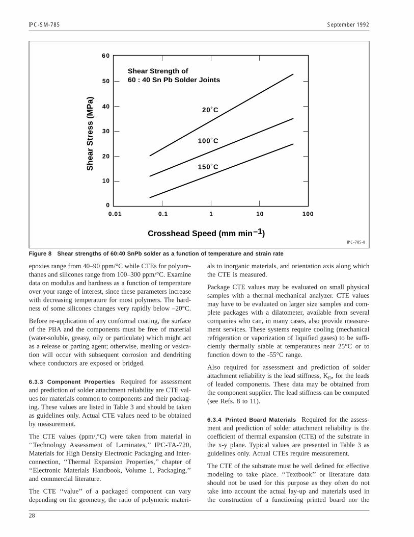
IPC-SM-785 September 1992
IPC-785-8
Figure 8 Shear strengths of 60:40 SnPb solder as a function of temperature and strain rate
60
50
40
30
20
10
00.01 0.1 1 10 100
Shear Strength of60 : 40 Sn Pb Solder Joints
20˚C
100˚C
150˚C
Crosshead Speed (mm min –1)
She
ar S
tres
s (M
Pa)
-inturasrdC
eiactcag
tl-geed
n,r-f
’
yri-
ich
icaluesom-ralure-icalfi-to
er
romted
-heinas
iveanot
ine
epoxies range from 40–90 ppm/°C while CTEs for polyurethanes and silicones range from 100–300 ppm/°C. Examdata on modulus and hardness as a function of temperaover your range of interest, since these parameters increwith decreasing temperature for most polymers. The haness of some silicones changes very rapidly below –20°
Before re-application of any conformal coating, the surfacof the PBA and the components must be free of mater(water-soluble, greasy, oily or particulate) which might aas a release or parting agent; otherwise, mealing or vesition will occur with subsequent corrosion and dendritinwhere conductors are exposed or bridged.
6.3.3 Component Properties Required for assessmenand prediction of solder attachment reliability are CTE vaues for materials common to components and their packaing. These values are listed in Table 3 and should be takas guidelines only. Actual CTE values need to be obtainby measurement.
The CTE values (ppm/,°C) were taken from material i‘‘Technology Assessment of Laminates,’’ IPC-TA-720Materials for High Density Electronic Packaging and Inteconnection, ‘‘Thermal Expansion Properties,’’ chapter o‘‘Electronic Materials Handbook, Volume 1, Packaging,’and commercial literature.
The CTE ‘‘value’’ of a packaged component can vardepending on the geometry, the ratio of polymeric mate
28
eee
-.
l
-
-n
als to inorganic materials, and orientation axis along whthe CTE is measured.
Package CTE values may be evaluated on small physsamples with a thermal-mechanical analyzer. CTE valmay have to be evaluated on larger size samples and cplete packages with a dilatometer, available from sevecompanies who can, in many cases, also provide measment services. These systems require cooling (mechanrefrigeration or vaporization of liquified gases) to be sufciently thermally stable at temperatures near 25°C orfunction down to the -55°C range.
Also required for assessment and prediction of soldattachment reliability is the lead stiffness, KD, for the leadsof leaded components. These data may be obtained fthe component supplier. The lead stiffness can be compu(see Refs. 8 to 11).
6.3.4 Printed Board Materials Required for the assessment and prediction of solder attachment reliability is tcoefficient of thermal expansion (CTE) of the substratethe x-y plane. Typical values are presented in Table 3guidelines only. Actual CTEs require measurement.
The CTE of the substrate must be well defined for effectmodeling to take place. ‘‘Textbook’’ or literature datshould not be used for this purpose as they often dotake into account the actual lay-up and materials usedthe construction of a functioning printed board nor th

d t
ofnt
intesio
-surot
eco
ted
seanthor
e-udhisgorr-
tout inse.ag-toglife
isese
i-ofge-teded.ail-icend
September 1992 IPC-SM-785
actual resin content achieved and may, therefore, leaerroneous results.
A means of obtaining this information is through the usestrain gauging in both the x and y directions (significadifferences have been measured) a representative prboard and passing the sample through a thermal excurallowing the CTE to be measured directly (see IPC-TM650, 2.4.41 and 2.4.41.1). Care should be taken to enthat a representative printed board is used and that bsides of the part are measured to check for warpage effas a result of unbalanced construction or delaminationthe constraining member from the active part of the prinboard.
The glass transition temperature of the material being ushould also be known and should not be approached attime during the test. The glass transition temperature istemperature at which an amorphous polymer (or the amphous regions in a partially crystalline polymer) will exprience a rapid change in its mechanical properties (incling CTE, yield and tensile strengths). Testing above ttemperature will result in the material not only exhibitinnon-representative mechanical properties during that ption of the test cycle but also, will often result in the oveall degradation of the polymer during the test cycle.
Table 3 Typical Valuesfor Coefficients of Thermal Expansion (PPM/°C)
Insulator/SubstrateMaterial/System
CTElower
CTEtypical
CTEupper
E Glass 5.5
S Glass 2.6
Glass-Ceramic >3.0
Silicon 2.6
Diamond 0.9
Aluminum Nitride 4.5
Silicon Nitride 3.7
Quartz, fused silica 0.5 0.6
Kevlar 49 –5
Beryllia 6
Cubic Boron Nitride X–YZ
3.77.2
E Glass/Epoxy X–YZ
1455
2090
E Glass/Polyimide X–YZ
1260
16
E Glass/PTFE X–YZ
24260
Kevlar/Epoxy X–YZ 5.1 7.1
Kevlar/Polyimide X–YZ
3.483
6.7
Quartz/Polyimide X–YZ
5.068.4
8.0
o
dn
ehtsf
dy
e-
-
-
Insulator/SubstrateMaterial/System
CTElower
CTEtypical
CTEupper
Quartz/Bismaleimide, X-Y35% Resin Z
6.241
6.3
Alumina (90%) TFSubstrate 7.0
Alumina (Ceramic ChipCarrier) 5.9 6.5 7.4
Epoxy (70% Silica) PlasticPackaging 20 23
Mullite Co-Fired 4.2
Alloy 42 4.4
Aluminum (40% Silicon) 13.5
Aluminum, T6061 23.6
Boron Aluminum (20%) 12.7
Copper, CDA 101 17.6
Copper/Invar/Copper20/60/20 Thick 5.7 5.8
Copper/Molybdenum/copper20/60/20 Thick 7
Gold 14
Graphite/Aluminum 4 6
Invar 36 1.6
Invar 42 4.5
Kovar 5
Lead 29
Lead (95%) Tin Solder 28
Lead-Tin Solder 60/40 23 25
Molybdenum 4.9
Ni-clad Molybdenum 5.2 6.0
Silver 19
Tungsten/Copper (90/10) 6.0 6.5
Tungsten 4
7.0 ACCELERATED RELIABILITY TESTING
The goal of an accelerated test is to produce failure oraccumulate damage by the same damage mechanism bless time than would be required during the product uThere are several general ways of achieving this. The mnitude of the life controlling variable can be increaseddecrease the life. The magnitude of the life controllinvariable can be maintained at the value expected in atest but applied more frequently, so that the test durationdecreased. It is also possible to do a combination of thtwo things.
It is important to understand what the life controlling varable (or variables) is, how it is influenced by the naturethe test being run, and how varying the rate and/or ranof application of this variable influences the life. It is critical to understand the relationship between the acceleratest and the actual service condition being acceleratOften the accelerated test produces a different type of fure or does not properly correspond to the actual servcondition. As such, it would not be a valid acceleration a
29

ingon-esis-plee
roully
mitly
isndi
sizeck,lureonthenvi
isanr-chatusle
nsil-
ivebil-edorga-
toel-
ingda-leheiheeste a
fre
t,ectri-am-
useforst
dises
s iner--
ha-se
ns.
sblere-s ofcha-
inldts,fer
ng
edsthecti-on-attheoflessue
inig-
in
licpo-/orm-
s,-age
IPC-SM-785 September 1992
should not be employed without a complete understandof how this accelerated test correlates with the service cdition. Without such an understanding, any inferencdrawn from the accelerated test are likely to be highly mleading and should, therefore, not be used. As an examit would be inappropriate to test from –55 to +125°C, if thservice environment is within –20 to +100°C.
Although the use of accelerated testing can be dangebecause of the introduced uncertainties, it is generaunavoidable because the design life is too long to permore realistic testing. It is therefore imperative to fulunderstand what the actual life controlling phenomenonand how the accelerated test is related to the service cotion.
Several different types of tests are available to emphadifferent failure processes. Thermal fatigue, thermal shoand/or vibration tests can be performed to accelerate faimechanisms controlling the solder joint life. The selectiof test type and test conditions should be based onappropriate damage/failure mechanisms and service eronment identified in Sections 3.4 and 3.5.
7.1 Reliability Program/Strategy Before embarking on areliability program it is important that an understandingreached as to the purpose of the program. The testinganalytical strategies can vary dramatically for different puposes. The definition of purpose will depend on how muis already known, what new information is required, whresources and how much time is available, what are theconditions for the product, the design life, the tolerabfailure risk, etc.
Figure 1 shows a flow chart with the steps and decisiothat might be followed to carry out an appropriate reliabity program.
For some use and loading conditions the quantitatunderstanding is not as yet adequate for analytical reliaity prediction; even relating the results from accelerattests to product reliability is beyond current capabilities fsome loading conditions. For this reason, generic investitions into damage mechanisms might be necessarydevelop appropriate reliability prediction models and acceration factors/transforms.
7.2 Generic Damage Mechanism Investigations Inves-tigations to gain qualitative and quantitative understandof damage mechanisms threatening reliability are funmentally different from accelerated reliability tests. Whiboth types of testing requires damage accelerations, tdifferent objectives impose different requirements on tlevel of control on parametric variations, sample size, tarrangements, measurement techniques, necessary timresources.
For example, while for reliability testing the definition ofailure should properly be related to the functional failu
30
,
s
-
-
d
e
r
nd
of the product, i.e, electrical discontinuity in a solder jointhe failure definition for generic investigations can takforms such as a decrease in strength, an increase in elecal resistance, an increase in thermal resistance, or a dage in characteristic frequency.
Generic investigations of this type are necessary becathey lead to the required understanding that is necessarythe development of reliability models, as well as the moeffective working conditions.
7.3 Thermal Cycling The damage mechanisms invokeby thermal cycling are described in Section 3.4.1. Itimportant that the thermal cycling test chosen producdamage in the solder joints by the same mechanism athe use of the product. There are three basic types of thmal cycling that can be employed: functional cycling, temperature cycling, and thermal shock. The damage mecnism for thermal shock is discussed in Section 3.4.3. Thedifferent test types are discussed in the following sectio
7.3.1 Functional Cycling Functional cycling, as thename implies, involves simulating operational conditionas closely as possible. This is done to eliminate intractaeffects on the test results of the many highly temperatudependent material properties. In this manner, the resultthe accelerated test will exclude extraneous damage menisms and reflect the conditions product experiencesoperation. The mimicking of operational conditions shouinclude power dissipation internal to the componencomponent-external temperature variations, heat transand thermal management conditions, and mountiarrangements.
Only one or two parameters should have well-controlldeviations from the operating conditions to facilitate teaccelerations and minimize uncontrolled influences. Tparameter that can be varied most easily, results in pracal test accelerations, and does not introduce undue ccern about different material behaviors is the dwell timethe steady-state temperature extremes. Decreasingdwell time results in significantly decreased degreescompleteness of solder stress-relaxation and, therefore,fatigue damage per cycle. While this results in more fatigcycles necessary to cause failure during the test thanoperational use, the mean-time-to-failure in the test is snificantly less because many more cycles are possiblethe same time frame.
Another acceleration option is an increase in the cycfatigue loads by an increased mismatch between comnent and substrate coefficients of thermal expansion andusing test components larger in size than the product coponents. Increasing the cyclic temperature swing,∆T, is nota good acceleration option for solder joint; in many casethe increase in∆T necessary for substantial testacceleration also causes the introduction of new dam

September 1992 IPC-SM-785
Table 4 Properties of Printed Board Laminates
MaterialConductivity
W/M-K
CTE X, YDir.
ppm/°C
CTE ZDir.
ppm/°C
Max. UseTemperature
°C
GlassTransitionTemp. °C
TensileStrength
MPa
YieldStrength
MPaElongation
%
Polymer Composites:
Polyimide Glass 0.35 12-16 40-60 215-280 250-260 345 — —
Epoxy Glassa 0.16-0.2 14-20 65 130-160 125-135 276 — —
Modified Epoxy Glassb — 14-16 — — 140-150 — — —
PTFEe Glass, Non-Woven 0.1-0.26 20 — 230-260 — 38-52 — —
PTFEe Glass, Woven 419-837 10-25 — 248 — 68-103 — —
Epoxy Aramid 0.12 6-8 66 — 125 — — —
Epoxy Quartz — 6-13 62 — 125 — — —
Polyimide Aramid 0.28 5-8 83 — 250 207 — —
Polyimide Quartz 0.35 6-12 35 — 188-250 — — —
Epoxy-Cordierite 0.9-1.3 3.3-3.8 — — — — — —
Modified Epoxy Aramid — 5.5-5.6 100 — 137 — — —
PTFEe — 7.5-9/4 88 — 19d — — —
Polyimide 4.3-11.8 45-50 — 260-315 — 345-965 — 6.7
Metal Composites:
Cu/Invar/Cu (20/60/20) 15-18c 5.3-5.5 16 — N/A 310-414 170-270 36
Cu/Invar/Cu (12.5/75/12.5) 14c 4.4 — — N/A 380-480 240-340 —
Cu/Mo/Cu 90-174 2-6 — — N/A — — —
Ni/Mo/Ni 129.8c 5.2-6 5.2-6 — N/A 621 552 50
a. FR-4, G-10 b. Polyfunctional FR-4 c. Z-direction d. Polymorphic p e. PTFE Polytetrafluoroethylene
tes
anhescescaat
r-mao-la
cae-
d fismod, alic
anju
rgetheesetalf
imenell
C/st
r theera-erend
silesesholdin
tedenssess ansol-
mechanisms and different material behavior putting theresults in question (see Section 4.0)
7.3.2 Temperature Cycling Temperature cyclinginvolves subjecting the test vehicles alternately to highlow temperatures for predetermined dwell times. Tchange in temperature should be accomplished at rateless than 20°C/min to avoid thermal shock. To producreep/fatigue damage the suggested temperature cycle+25 to +100°C or 0 to +100°C depending on the applition of the product (see Table 1) with 15 minute dwellsthe temperature extremes.
Depending on the application, ‘‘Cold’’ cycling from pehaps –40 to 0°C with dwells large enough to reach therequilibrium can be employed. This kind of cycling prduces fatigue damage that does not involve stress reation and creep of the solder.
For applications where large cyclic temperature swingsoccur in product, e.g., Use Category 9 – AutomotivUnderhood (see Table 1), ‘‘Large∆T’’ cycling similar innature and number to the temperature swings expectethe product are recommended. The damage mechaninvoked are numerous, interactive and not well understotest results from this kind of temperature cycling cannotthis point in time, be related to different temperature cycconditions.
It is important that these temperatures, and heatingcooling rates be measured on the specimen and not
t
d
of
are-
l
x-
n
ors
;t
dst
inside the thermal cycling apparatus. There can be ladifferences in the response of a specimen and that ofapparatus used for heating and cooling. Furthermore, thdifferences will depend upon variables such as the tothermal loading, which is a function of the number ospecimens being tested, the thermal mass of each specand that of the apparatus, the specimen distribution, as was the flow rate of the air.
7.3.3 Thermal Shock Cycling For a discussion of thethermal shock mechanism see 3.4.3.
In this type of test a heating and/or cooling rate of 30°minute or greater is employed. The severity of the teincreases as the temperature range gets larger and/orates of temperature change increase. The mean tempture change developed in this type of test leads to sevtemperature gradients which distort the printed board athe component, and leads to the development of tenstresses in the solder joints. In addition, shearing streswill develop from the thermal expansion mismatcbetween the component and the printed board. Long htimes can allow these distortions to be relaxed by creepthe solder joint between the component and the prinboard. This adds to the damage of the joint and shortthe cyclic life. Increasing the temperature range increathe thermal stresses and also decreases the life, as doeincrease in the mean temperature which increases theder creep rate.
31

lingeri-rmarise
tosilepr
adsandualperm-raterallyuteThepatat-
ri-red
ingof
cal
theut
lingturermangiateryas
toaustesntss i, or
ounbl
eduit-emthe
nicaol-for
e-ealhey
el-dd
aly-en-of
hatst
ra-tralv-ed
s ispe-
rmsctracy
-p-ci-ra
ri-d-ine
o-fre-ellthec-
insi-nd
IPC-SM-785 September 1992
The distinction between thermal shock and thermal cycis not always addressed in designing reliability expments. There is a fundamental difference between theshock and thermal cycling. The primary differences afrom the mechanism of loading. Thermal shock tendsresult in multiaxial states of stress dominated by tenoverstresses and tensile fatigue. On the other hand, asviously discussed, thermal cycling results in shear loand failure occurs from an interaction of shear fatiguestress relaxation. Thermal shock is performed in dchamber test equipment, whereas thermal cycling isformed in single chamber cycling equipment. Dual chaber arrangements can produce temperature transitionin excess of 50°C/minute. Most single chambers genedo not produce transition rates even close to 30°C/minwhich is the rate necessary to induce thermal shock.results of these two types of testing are generally incomible. Finally, thermal shock testing for purposes of evaluing surface mount solder joint reliability is only appropate if thermal shock is indeed a field condition encounteby the product.
In some specifications, the definitions of thermal cycland thermal shock are not fully differentiated; the rateschange are more closely associated with what we areing thermal shock.
7.4 Mechanical Cycling In mechanical cycling theattempt is made to produce solder joint failures bysame damage mechanism as in temperature cycling, bsignificantly higher test accelerations. Mechanical cycis carried out at constant temperatures; higher temperaproduce larger test accelerations. Because isothemechanical cycling is not subject to the relatively lotimes required to reach, and the uncertainties assocwith, thermal equilibrium, cycle frequency can be vehigh with dwell times at the cyclic motion extremesshort as a few seconds.
A way to accelerate the mechanical cycling test isincrease the applied loads. This is a simple matter becthe loads are applied by mechanical deformation of thevehicle substrate or external loading of the componeCare must be taken during the test to prevent changesolder joint failure due to overstressing, high strain ratechanging from predominant shear to tension fatigue.
Practically, the test specimen consists of a surface mcomponent soldered on a printed board, with the assemmodified to allow for a mechanical loading. The printboard can be pulled or bent and it is possible, with a sable adhesive, to pull on the component. Since the tperature is kept constant, the thermal properties ofspecimen are not critical.
Because this type of testing neglects all thermo-mechaeffects, this test is useful for comparisons of different sder attachment designs. However, it cannot produce in
32
l
e-
-
s
-
l-
at
sl
d
et.n
ty
-
l
-
mation that can be used to directly produce reliability prdictions for product. Mechanical cycling can bbenchmarked with thermal cycling, not including thermshock, to allow some estimate of product performance. Tneglect of all thermo-mechanical effects, which do plaimportant roles in solder fatigue, as well as the high acceration factors reduce this type of test to a ‘‘quick andirty’’ compromise necessitated by the realities of limitetime and resources.
7.5 Vibration
7.5.1 Vibration Environment
7.5.1.1 Random Vibration The majority of vibrationexperienced by electronics has been determined by ansis to be broadband in spectral content. That is, all frequcies are present at all times in various combinationsintensity. Controlled experiments have demonstrated trandom vibration effectively simulates broadband in a tesituation.
Random vibration spectra are defined in terms of acceletion spectral density (also referred to as power specdensity, or PSD) profiles, which relate energy density leels to specific frequency bands. The vibration is definover a relevant frequency range.
The use of g-rms values alone to describe vibration testnot valid, since a g-rms value does not characterize a scific vibration profile. An infinite combination of frequencybandwidths and spectral shapes can satisfy one g-value. Therefore, vibration measurements and test speshould always relate energy content to specific frequenbands.
7.5.1.2 Source Dwells In some cases, the vibration environment is characterized by periodic excitation from recirocating or rotating structures and mechanisms. This extation may be transmitted through fluids (air or liquid) ostructures. When this form of excitation predominates incritical frequency band, source dwell vibration is appropate. A source dwell excitation is characterized by broaband random, narrowband random, or one or more swaves.
This technique differs from the traditional sinusoidal resnance dwell test. A resonance dwell emphasizes thosequencies at which the test item resonates. A source dwemphasizes those frequencies which predominate inplatform environment. Obviously, the source dwell spetrum provides a more realistic test.
7.5.1.3 Sinusoidal Vibration The service vibration envi-ronment in some propeller aircraft and helicopters contaexcitation which is basically sinusoidal in nature. The exctation derives from engine rotational speeds, propeller, a

ahist bsont
ene
ntu-, te.enheoibt
inhe
nfre
av
-ra-yal
that-elsv-aniner-ncthtesa-ly
tost-tin
eone
SDisede-be
thea-3
onofonesy
oralf arear-
-isarep
atoteeofurs
nsnk-nd
September 1992 IPC-SM-785
turbine blade passage frequencies, rotor blade passagevelocity, and their harmonics. Environments such as tmay be best simulated by a sinusoidal test. Caution musexercised to assure that the frequency range of the sinudal exposure is representative of the platform environme
7.5.1.4 Mechanical Impedance Effects Allowanceshould be made for mechanical impedance effects whever the benefits of increased realism are worth the timeffort, and cost required for implementation.
Equipment structures dynamically influence their owresponse to an external forcing function. At structural naral frequencies where the response stresses are highstructure will load the adjacent supporting structures (i.notch the acceleration spectral density at these frequcies). The magnitude of loading effects is related to trelative impedance of the equipment structure and suppstructures. As a rule of thumb, the resonant element exhits a loading force in proportion to its dynamic weighmultiplied by the corresponding amplification factor.
Mechanical impedance effects can be accounted forestablishing vibration test spectra. The depths of notcare determined by measurement or by calculation.
7.5.2 Vibration Acceleration Vibration testing is recom-mended to be performed only with careful fixturing or ocomplete systems in order to include accurate naturalquency responses and use conditions.
There are three different types of vibration tests, each hing a different purpose.
1. The vibration functional test is to verify that the equipment functions at the maximum expected service vibtion level. The duration of the functional test is typicallonly long enough to verify equipment function or a totof one hour per axis, whichever is greater.
2. The endurance test is conducted to demonstrate thatequipment has a structural and functional life compible with contract requirements. Endurance test levand durations are established by raising functional leels and extending the test duration to generateequivalent lifetime fatigue damage. This resultsvibration test levels higher than maximum expected svice levels, in some cases much higher. The enduratest does not necessarily establish fatigue life sinceequipment is not tested to destruct. The enduranceis only conducted for a prescribed period of time. Sttistically the sample size is also too small to adequatedetermine fatigue life.
3. In accelerated life testing the equipment is testedfailure by raising functional levels as in endurance teing, but the test is continued until failure. Multiple tesvehicles must be used to gain a statistical confidencethe accelerated fatigue life.
nd
ei-.
-,
he,-
rt-
s
-
-
e
eet
A simplified fatigue relationship is often used to scalvibration levels, test durations, and derive acceleratitransforms when the loading is random vibration. Thequation relates two test conditions, 1 and 2,
[PSD1
PSD2]M
=t2t1 (19)
where
PSD = acceleration power spectral density (G2/Hz)t = time (consistent units of seconds, minutes,
or hours)M = material constant
and represents a linear log-log relationship between Pand time, where the negative slope is 1/M when timeplotted on the horizontal axis. Equation (19) can be relatback to Basquin’s high cycle fatigue relationship or thcommonly recognized S/N curve, linear log-log relationship between stress and cycles to failure. Care mustexercised when comparing the two relationships sinceslopes of the two curves vary by a factor of two. For eqution (19), a starting value of M for solder attachments isto 4.
Small variations in the exponent value M used in equati(19) can make dramatic variations in the predicted lifean assembly when the equations are used to scale fromcondition to another. A potential for extrapolation error iparticularly true when the lives of the two conditions varby more than a decade.
The simplified fatigue relationship in equation (19) is alsquestionable under high vibration levels due to structunonlinearities. During accelerated testing, use as long otest duration as practical to keep vibration levels low. Mosophisticated analysis techniques can be used when wranted.
7.6 Creep Rupture Tests Creep rupture tests are generally performed under constant load conditions. A loadapplied to the specimen and the time dependent strainsmeasured with an LDVT or extensometer. A typical creerupture test is shown in Figure 9.
Generally, metals will show three distinct regions increep test. Region I is primary creep. This region tendsbe very small in solder alloys. Region II is steady-stacreep in which the strain rate is relatively constant. Thsteady state region is of particular interest in the analysiscreep-fatigue interaction since steady state creep occduring hold times.
Region III is tertiary creep in which cracking in the grainboundary occurs rapidly until failure. The test specimeare very important. Microstructure has a primary effect ocreep behavior of solders. The test joint dimensions (thicness) must be representative of joints in service. Plug a
33

IPC-SM-785 September 1992
IPC-785-9
Figure 9 Creep behavior of solder
TIME
ST
RA
IN
XX
T1
T2
III
III
Rupture
III
T2 > T1
or
ndudsen.rises
i0
dsith
delieheatuemnercaheeto
forbo
edge
d-blet of
e
beMste;itsest
ton a
eders.
ttedlts-riaertal
ring joints or lap joints provide the best configurations fcreep testing of solder alloys.
7.7 Mechanical Shock Testing Mechanical shock testsare high acceleration tests that simulate severe use cotions or even accidental misuse. These conditions inclsuddenly applied loads or abrupt changes in motion cauby rough handling, transportation, or field operatioShocks in this category may disturb operating charactetics or cause damage similar to that resulting from excsive vibration.
In a mechanical shock test, very rapid and sharp cyclingarranged. Typically, the shock pulses are 500 to 30,00with a pulse duration between 0.1 and 1.0 milliseconThis rapid mechanical cycling enables tests to be run wvery small applied loads or displacement ranges.
Mechanical shock is characterized by peak amplituduration, and time rate of change and is generally appto a system in the form of a pulse, impulse or step. Tsystem response to the shock is dependent upon the nof the shock, the architecture and materials of the systthe orientation of the system with respect to the shock athe natural frequency or frequencies of the system. Whthe duration of the pulse or step is short, the systemvibrate at its own natural frequency or frequencies; tamplitude of that free vibration will decrease with timdepending upon the damping available in the systemdissipate the mechanical energy as heat.
Mechanical shock tests are intended to quantify the permance of the product or component under controlled laratory rather than actual field conditions because:
34
i-ed
--
sg.
,d
re,
den
--
1. The shock waveform can be controlled and reproducfor comparison purposes and can be varied over a ranwhich is representative of a wide distribution of fieldconditions.
2. The laboratory environment permits the realtime recoring and analysis of the shock and responses, possiimprovement of the assembly, and rapid reassessmenthe new construction.
3. Many laboratory tests can be performed for the samcost and time required to run several field tests.
The shock waveform of mechanical shock machines canaffected by the mass and mass distribution of the Sprinted board assembly particularly if the mass of the tespecimen is significant compared to that of the machinthe shock machine should be as rigid as possible withnatural frequencies well above those expected in the tspecimen.
The shock waveform can be specified as that expectedbe applied to the test specimen or as that expected whespecific shock machine is employed.
Shock machines range from simple drop table and inclinplanes testers to high acceleration gas and air gun test
7.8 Failure Criteria for Solder Joint Fatigue Tests Thedefinition of failure of a solder joint and its subsequendetection are not as straight-forward as might be expec(see Section 4.3.1). Frequently, comparison of test resuhas been made difficult, if not impossible, by failure criteria which cannot be related to each other. These critehave included visual inspection for cracks in the soldjoints at periodic intervals, destruction of solder joints aperiodic intervals searching for decrease in the origin

ficasishes
hestltsagerre
oledn-al
of
orrin
te
noisreeds
ur oder
int
nyaistht.
ianelbeleteen
these
stld
he
nti-helet-
y
)are
set-
fulld-
heu-ent.)
m
ofter-sonis
ebe
September 1992 IPC-SM-785
strength, monitoring the stress-strain hysteresis loopsindividual solder joints and defining failure in terms osome hysteresis loop characteristic, monitoring electrresistance for some amount of increase in original retance, and monitoring for electrical resistance with tcapability of detecting even short electrical discontinuitie
Failure criteria that require the periodic interruption of ttest may significantly prolong the time required for the temay disturb the experiment, and influence the resuChoosing arbitrary failure definitions can serve as damindicators if they are carried out consistently. Howevgiven the many different failure definitions and measument techniques used do not make comparison easy.
For the purpose of accelerated reliability testing, the flowing failure criteria are recommended. Failure is definas the first interruption of electrical continuity that is cofirmed by 9 additional interruptions within an addition10% of the cyclic life.
Failure detection shall be by continuous monitoringdaisy-chain continuity test loops such that:
1. At least one continuity interruption of 1 microsecondless duration can be recorded for each test loop duany polling interval of 2 seconds or less;
2. At least 10 such interruptions can be recorded perloop to confirm the first failure indication;
3. The monitoring current does not exceed 2mA atmore than 10V and that an electrical discontinuityindicated by a loop resistance of 1000 ohms or moFalse failure indications due to electrical noise can bproblem, particularly for loop resistance threshollower than 1000Ω.
These guidelines reflect the limitation of available continity monitoring devices, as well as the observed behaviodaisy-chain test loops with fractured solder joints. It neeto be pointed out that multiplexed monitoring, no matthow fast, isnot continuous monitoring and will lead tofailure detection significantly later than when solder jofracture occurs.
7.9 Accelerated Life Test Planning Determining themethodology for an accelerated life test is similar to adesign of experiment concept used in industry to evalua process of a product. In reliability performance itimportant to establish the correlative parameters ofaccelerated stress exposure to the end-use environmen
In the design of an accelerated life test experiment itimportant to test one or more independent variablescompare those to a dependent variable. In solder joint rability testing the single dependent variable is the numof cycles to which an equipment is subjected. Cycmimic the electronic equipment operation, and are relato the conditions of the end-use environment. The indepdent variables can then be equated to:
of
l-
.
,.e,-
-
g
st
.a
-fs
te
e
sdi-r
sd-
• Temperature Swings, e.g., +25 to +60°C
• Component Size
• Coefficients of Thermal Expansion
• Solder Joint Height
• Lead Stiffness
• Failure Probability
7.9.1 Test Variables A design of experiment shoulddefine all the appropriate parameters that are part ofexperiment. This includes identification of the responvariables being studied.
The test objective should be defined by detailing the tequestion, null hypotheses, optimization, etc. There shoube no doubt what the purpose of the test is or why texperiment was conducted.
Independent variables need to be characterized and idefied in great detail with specific emphasis placed on trelationship of the variables to the dependent variabbeing studied. The independent variables fall into four caegories. These are:
• Design Parameters
• Process Parameters
• End Product Parameters
• End-Use Environmental Parameters
• It is important to define the rational for selection and wheach independent variable is included in the plan.
7.9.2 Test Plan The test plan should indicate the level(sor range of values at which the independent variablesevaluated.
These levels(s) are the test setting and the reason forting the ranges needs to be defined.
The test plan should describe the experimental design (factorial, fractional factorial, etc.) used for the study anthe method in which the experiment is performed (randomized, stratified, production equipment, laboratory, etc). Tmeasurement method is identified in this plan. This is usally the physical method used for measuring the dependvariable (e.g., solder joint fracture giving the fatigue lives
An example of a test plan is the IPC Round Robin Progra‘‘Evaluation of Surface Mount Land Patterns,’’ defined inIPC-SM-782,’’ August 1988.
7.9.3 Sampling Methodology The sample size and fre-quency is identified in the plan. Included are the numberobservations on the dependent variable and the time inval between samples at a single test condition. The reawhy the sample size and frequency were selecteddefined.
Due to typical failure distributions associated with fatigutesting, a minimum of 32 data points has been found to
35

g.,ble
ataf
sinirer-tha(s)
ingro-f athirge
ing
dsearebe
ibleesege
ec-nd
r o
ure
tingctedveoddthe
See
atedtheer-
ngs autles
pos-es-
ctualuctpo-k-ill
es-of
one
innotcuranyer-the
ng/ngofsonderainhisted
anfor
tesibleundhisa-to
IPC-SM-785 September 1992
required, per test condition, to allow for test results (e.mean cycles to failure) to be calculated with reasonastatistical certainty.
Some care should be taken in the use of the term ‘‘dpoint.’’ If testing is concerned with the relative merits oone land pattern design vs. another, then 32 parts ueach of the two test land pattern designs would be requand individually monitored to allow for reasonable diffeentiation. It should be reasonable and in fact desirable,these test land concepts coexist on the same substraterule out any other random effects.
If on the other hand, another macro variable was beconsidered, say, printed board construction or reflow pcess parameter, then each data point would consist oentire assembly run separately through the process. Ininstance, it may be more cost effective to fabricate a lanumber of small, simple assemblies.
7.9.4 Test Vehicles The test vehicles (TV) must bedesigned to accommodate continuous electrical monitorduring the complete thermal cycle. (See Figure 10)
All components will be specially prepared to have leainternally interconnected so that in conjunction with thTV substrate pattern complete test loop daisy-chainsformed. It is preferred that these lead connectionsaccomplished internal to the packages wherever possHowever, for some components (e.g., chips, MELFs) thlead connections are only possible external to the packaIt is imperative that these internal or external lead conntions do not become a source of continuity disruptions athus falsely indicate surface mount attachment failures.
The lead connection scheme depends on the numbeI/Os of the component and is as follows:
2 I/O:Connect the two terminals.
3 I/O:Connect all three terminals together (as shown in Fig11).
IPC-785-10
Figure 10 Example of circuit layout
36
gd
tto
ns
,
.
.
f
4 or more I/Os:Connect only leads on the same component side. Starat the corners, alternate lead pairs should be conneinternally working towards the center of the respecticomponent side. For component sides that have annumber of leads, the center lead is not connected intotest loop and is skipped in the connection scheme (Figure 11).
Test vehicles should represent the product to be evaluin as great a detail as possible within the confines ofvariables being considered. For example, in the considation of solder joint design, testers often opt for deletithe constraining core (and thus increasing the CTE) ameans of accelerating failure. This technique is valid, bcare must be taken that in deleting the core other variabbesides the CTE are kept as close to the product assible. Measurement of the CTE values is absolutely necsary.
7.9.5 Sample Conditioning Test vehicles should beassembled and processed as similarly as possible to aproduct. Product-similar test vehicles should reflect prodsolder joint characteristics such as grain structure, comsition, and intermetallic compound layers and their thicness. Solder grain structure is inherently unstable; it wcoarsen with time and temperature, particularly in the prence of cyclic strains. In product, significant coarseningthe solder grain structure has been observed withinyear of storage.
Fine grain structures in the solder joints will resultlonger fatigue lives in accelerated testing, which doesallow the time for these time dependent processes to octo the same degree as they would in product use over myears. The changes in the structure of solder, which undgoes and accumulates fatigue damage, appear to followsequence of grain structure coarsening, micro-voidicavitation-formation at grain boundaries, micro-crackiwith 50 to 70 percent of life remaining, coalescencemicro-cracks, and fracture. Therefore, it stands to reathat accelerated test vehicles should start with a solgrain structure that is more representative of the grstructure in product after some period of operation. Tbecomes particularly important for more highly acceleratests.
After assembly, the test vehicles should be subjected toaccelerated thermal aging (e.g., 300 hours at 100°CFR-4, 100 hours at 125°C for polyimide) in air to simulaa reasonable use period and to accelerate such posprocesses as solder grain growth, intermetallic compogrowth, and oxidation. Storing the test vehicles after tartificial aging for some additional time at room temperture before commencing with the fatigue testing servesfurther stabilize the solder structure.

September 1992 IPC-SM-785
IPC-785-11
Figure 11 Internal lead connection schemes for odd lead numbers per side
SOT 23
3
1 2
12345678
910111213141516
DIP
44 I/O PLCC-J
123456
789
1011121314151617
18 19 20 21 22 23 24 25 26 27 28
2930313233343536373839
4041424344
12
34
56
78
910
1112
2423
2221
2019
1817
1615
1413
24 I/O SOIC-L
123456789 6162636465666768
1011121314151617181920212223242526
27 28 29 30 31 32 33 34 35 36 37 38 39 40 41 42 43
6059585756555453525150494847464544
1234567891011121314151617181920212223242526272829303132333435363738
90898887868584838281807978777675747372717069686766
100 99 98 97 98 97 96 95 94 93 92 91
54 55 56 57 58 59 60 61 62 63 64 655351 5249 5047 4845 4643 4441 42
100 I/O PLCC-L
6-8 I/O PLCC-J &6-8 I/O CLCC-J
ofenl aaryifi-rdbet
sejorth
ed
eealless
orng
geea-
ting.
etiontheoardr ofp to
beroingher
ofari-
ardillmay
7.9.6 Temperature Cycle Selection and Monitoring
The cyclic temperature profiles are a very important partthe test conditions. They should be measured on differparts of the test vehicles and the thermal load, as welfor the chamber environment itself. This is necessbecause 1) cyclic temperature profiles can vary signcantly for different parts (component versus printed boacenter versus edge of thermal load, etc.), and 2) chamenvironment can be significantly different for differenlocations within a chamber.
Temperature extremes in thermal cycling may be increaover those seen in the field, but only where no machange of material properties is seen as a result ofincrease. Appropriate temperature regimes are suggestTable 1. Examples of poorly selected extremes are:
a) The low temperature selected is greatly below that sin the field, and as a result, the solder has substantidifferent material properties than it would have in thuse environment (for example, little, if any, creep/strerelaxation).
b) The high temperature selected comes close to the Tg ofthe laminate material being tested.
ts
,r
d
ein
ny
Selection of sufficient dwell times is essential to allow fsignificant stress relaxation in the joint before beginnithe next thermal transition.
Because thermal shock tests involve different damamechanisms than creep/fatigue, ramp rates should be msured at the printed board assembly surface during tesand should not exceed 20°C/minute for thermal cycling
7.9.7 Sample Fixturing and Placement Within the Cham-
ber Attention should be given to the fixturing of thsamples under test, as the effect of position and orientawithin the chamber can often have major impacts onramp rates and temperatures seen by a given printed bassembly during test. It is recommended that a numbeprinted board assemblies be measured during test set uensure uniform temperature and air flow in the chamduring the test. As a further safeguard, samples undergtesting should not be grouped by test condition but ratshould be randomly arranged to prevent contaminationthe data by an uncontrolled or unanticipated chamber vability.
Finally, care should be taken to see that the printed boassembly is tested within the environment in which it wsee service. If a truly representative test is needed, this
37
ironffecard
dedcanbed toto
edin
on,sin
thhe-
heite.
gesst-
llysultithhic
s o
da-rse
aat
oml-
ntses.caiveenchcewthe
oruge
titutals
for-ureresseenighisue
theces.
-n,infrac-
r,
omi-tingd,
vail-oreril-
trapper-erys ishe
vedorly-
m-om-hecial
tion,0,h-insi-
iveal
int
IPC-SM-785 September 1992
require that a chassis representing the actual use envment be used within the chamber as this can greatly athe ramp rates and dwell times seen by the printed boassembly under test.
Connectors within the test chamber should be avoisince during thermal cycling the connector connectionsgive false failure indications. If connectors cannotavoided within the test environment, the connectors neehave high-quality, gold-plated connections not subjectsignificant movement during thermal cycling.
7.9.8 Data Analysis The test results need to be analyzand evaluated using statistical considerations to determfailure distributions, variable independence or interactianomalies, etc. Further, the data needs to be analyzed uthe information in Section 4, to verify corroboration wioriginal predictions, determination of differences in t‘‘non-ideal’’ factor, F, correlation of the effects of the different independent variables, etc.
Anomalies and deviations need to be examined as to tpossible causes to separate and identify the affects ofvariations from those caused by test vehicle differences
7.10 Failure Mode Analysis Failure mode analysis(FMA) can give valuable information as to the underlyincause(s) of failure. This is equally true for product failurand for evaluating the results of accelerated reliability teing. For accelerated reliability testing FMA is especiavaluable to determine the cause(s) of unexpected reand anomalies. FMA starts with visual analysis wincreasing magnifications, progresses to metallograpexamination, and, if necessary, to analytical techniqueSEM, EDX and Auger.
The metallographic study of solder joints and the elucition of the cause(s) of failure are complicated. Coagrains and colonies may arise from very long exposurerelatively low temperatures or from short exposureshigher temperatures under cyclic stress. Intermetallic cpound (IMC) layers may be formed during the initial sodering process, during rework to neighboring componeor during long service under relatively mild temperaturThe physical analyst is expected to comment on the lotion and quantity of intermetallics, the nature and relatdimensions of the grains, the possible sequence of evthat led to the joint failure and methods of avoiding sufailure in the future. Selective etching of the failed surfacan develop structures characteristic of rapid grain groin molten solder or slow grain growth by diffusion in thsolid state. SEM/EDX (Energy Dispersive X-Ray)Auger Scanning Electron Microscopy techniques can ament optical microscopy by providing quantitation of threlative abundances of tin, lead, copper and other consents of the solder joint; this data can identify those meand their source(s) which can lead to loss of ductility.
38
-t
e
g
rst
s
r
t
-
,
-
ts
-
-
The fracture surface appearance provides additional inmation on the fatigue mechanism. A transgranular fractsurface is characteristic of over-stress fatigue. Over-stdominated fatigue occurs when the solder joint has bexposed to high stress levels, typically due to very hstrain-rate loading. An intergranular fracture surfacemore characteristic of creep-fatigue failure. Creep-fatigfailure occurs at low stress levels. See Volume 12 ofMetals Handbook for examples of these fracture surfa
SEM/EDX is discussed in ‘‘Solder Joint Reliability,’’ Chapter 6. See Volume 9 of the Metals Handbook, 9th Editiofor a discussion of metallography; Volumes 10 and 12the same series discuss materials characterization andtography.
7.10.1 Optical Microscopy Interpretation of the cut/polished or etched solder joint specimen requires:
a. accumulated experience on the part of the analyst o
b. access to, and comparison with, representative photcrographs of solder and solder joint specimens resulfrom known applied stress and carefully describereproducible specimen preparation technique.
Photomicrographs of these kinds of specimens are aable from the International Tin Research Institute (ITRI)Tin-Information Center publications #580 and #703. Othphotomicrographs are available in ‘‘Solder Joint Reliabity,’’ Chapter 6 and 7.
7.10.2 Metallographic Preparation Preparing tin-leadsolder joints for metallographic evaluation requires excare. The samples are composed of high hardness (CoTin) intermetallic compound particles dispersed in a vsoft (Lead, Lead-Tin) matrix. This heterogeneous mascoated on a hard basis material of copper or iron alloy. Tlead-tin matrix can recrystallize at temperatures achieduring the curing of some epoxy mounting materialshardening of some thermoplastic mounting materials; poester or acrylic mounting materials with as LOW a teperature rise during cure or setup as possible are recmended. Great care is required in revealing tundeformed, undamaged structure under the superfilayer.
General comments on metallographic sample preparamounting, and polishing can be found in IPC-TM-652.1.10 and 2.1.1.2, in IPC-MS-810, ‘‘Guidelines for HigVolume Microsection,’’ and in Leco Corporation’s ‘‘Metallography Principles and Procedures’’ which also contareprints of ASTM E407-70 and ASTM E340-68. In addtion, pages 5–12 in the ITRI publication 580 are instructin dealing with tin-lead solder joint destructive physicanalysis (DPA).
7.10.2.1 Cutting The initial step for metallographicpreparation is the isolation of the component or solder jo

terci-
ini-
ci-f
thatal
is
s-eci-be
tond
t
abeheic
f ofap-
ndndls
u-sosol-nt-uc-ct
e:
cllydof
been-d-
sh-
ovemegingreby
tyaes
uct
ly.sh-hating
elden
at.toay
b-
regpli-avetwo
nse
toer-e00
ed.
thekeptur-
gcanthe
by
rom
September 1992 IPC-SM-785
for mounting. This entails the use of a jeweler’s saw, rouabrasive saw, or similar cutting device to remove the spemen. Several factors should be considered during thistial step:
1. Cut Location:Care must be taken to remove the spemen without cutting too close to the solder joint ointerest. The cut should, however, be close enoughexcessive grinding is not required. If in doubt, leavelittle extra material. Usually 1/10 inch of materiaaround the area of interest is sufficient.
2. Fixturing: Care must be taken to ensure that damagenot done to the specimen while holding it for cutting.
3. Cutting Speed:A smooth, consistent feed rate and presure should be maintained to avoid damaging the spmen. Vibration of the specimen during cutting mustavoided.
4. Cutting Fluids: Oil, water, or other types of coolanshould be used with abrasive blades, especially diamblades. The cutting fluid serves two main purposes:
1. Removal of the cutting debris, allowing for efficienmaterial removal.
2. Removal of heat generated during cutting. Whensituation requires dry cutting, extreme care musttaken to avoid generating heat which may affect tspecimen, particularly solder joints or polymermaterials.
A coolant should be chosen which can be cleaned ofthe specimen easily and completely, so that the encsulating epoxy can bond to the sample surface.
5. Ceramic Precautions:Due to their hardness, aluminumoxide ceramic specimens require the use of diamobonded cutting equipment during both cutting agrinding. Also, beryllium and beryllium oxide materiaproduce toxic dust and must never be cut dry.
7.10.2.2 Mounting The specimen should be encapslated in some rigid medium for grinding and polishing,as to achieve a flat, uniform surface and to protect theder joint. Caution must be used to ensure that the mouing procedure does not change the solder joint microstrture. Overplating with copper or nickel can help to protehighly deformable materials. Two mounting methods ar
1. Quick Mounting:This method utilizes a thermoplastimaterial such as polymethylmethacrylate, and typicais not entirely transparent. Filling of small cavities anadhesion to the sample may be inferior to the resultsslow mounting. However, one mount can usuallyprepared in approximately 5–15 minutes. The heat gerated by quick mount systems varies widely from prouct to product.
2. Slow Mounting:This method typically utilizes epoxideas the mounting media. Vacuum impregnation tec
niques can be used to remove air bubbles and imprflow of the encapsulant into confined spaces. Soencapsulants must be cured at temperatures ranfrom 60 to 90°C, while others are room temperatucuring, but can generate even higher temperaturesexothermic reactions. Experimentation with empmolds will reveal whether this is a problem. Curing inwater bath helps to remove excess heat. Mounting timcan vary from 1 to 8 hours depending upon the prodand the curing conditions.
7.10.2.3 Preparation for Mounting When mounting aspecimen, it is important that it be oriented properProper orientation depends upon your grinding and poliing equipment and technique. Practice will determine wworks, and what does not. Here are two basic mountmethods:
1. Vertical Mounting:The sample is held vertical relativto the bottom of the mold either by gluing it to the mofloor or by using special clips. The encapsulant can thbe poured into the mold until it is full.
2. Half-Mounts: The sample is placed horizontally intomold which is half full of previously cured encapsulanThe mold is then filled with encapsulant and allowedcure. The sample is then ground from the side, and mnot fit into some automatic machines. If this is a prolem, then vertical mounting should be used.
Note:The grinding and polishing sections of this proceduwere written from the point of view of manually grindinand polishing the sample. Most of the concepts are apcable, however, to automatic processing. Attempts hbeen made to reconcile the differences between theprocedures.
7.10.2.4 Grinding The third step of sample preparatioinvolves removing material from the specimen to expothe areas of interest. Grinding is an abrasive processslowly remove deformed surface material and reveal undlying, nondeformed regions. Grinding is typically donusing silicon carbide papers, progressing from 120 to 10grit depending on the amount of material removal requirSeveral factors should be considered during this step:
1. Pressure:Sample hardness dictates, to some extent,amount of pressure required. Pressure should belight to avoid excess deformation of the specimen sface.
2. Time: The grinding time for each piece of grindinpaper should be kept short. Excessive grinding timecause faceting as the grinding paper wears down andparticles get dull. Faceting is usually correctedswitching to a new, sharp piece of grinding paper.
3. Cutting Fluid: As with the cutting operation, fluid isused to remove debris and prevent the specimen foverheating. Water is the most common cutting fluid.
39
s,me
ngucussuAchusia
isflathn
es
inakllyta
iccth
ludmou
tchmrs
hae aheapfteiveids
gr-hor-al
ingur-
in-
deria.
oftoayingsedlly
t.
ou,
leheallis
neddedly
-am-
clu-n,
lies.ma-en.allyfor
teseavyryllia
alsionho-
l
nol
IPC-SM-785 September 1992
4. Ceramic Materials:Due to the hardness of ceramiccomponents, packages and substrates made of cerasuch as aluminum oxide (alumina) or beryllium oxid(beryllia) require the use of diamond bonded cuttiwheels and grinding disks. Mechanical processes sas grinding and polishing of beryllia pieces create a ddefined as a hazardous material; this dust must bepressed by sufficient coolant and cutting fluid. OSHand EPA handling requirements will supersede any tenical handling or use requirements. The beryllia dmixed with the fluid is defined as a hazardous materthis aspect must be considered during disposal.
5. Viewing Window:Often during precision grinding it ishelpful to look clearly at the sample from above. Thcan be accomplished by grinding and polishing aarea on the surface of the epoxy perpendicular tosectioning plane. Some automatic equipment doesallow mounting of these irregularly shaped samplhowever.
6. The hard intermetallic compounds such as Cu6Sn5,Cu3Sn, Ni3Sn2, Ni3Sn7, AuSn, AuSn2, AuSn4, FeSn,FeSn2, and Ag3Sn can cause grooves and channelsthe soft lead or lead-tin matrix when the particles brefree and roll downstream. Manually or automaticamoving or rotating the sample counter to the wheel rotion will minimize grooves and channels.
7.10.2.5 Polishing The next stage of metallographpreparation following the grinding step is polishing the setioning plane. Polishing is a less severe continuation ofspecimen surface abrasion. Polishing media can incdiamond, aluminum oxide, silicon oxide, or chromiuoxide. Polishing media particle size progresses from ab9 µm to as fine as 0.05 µm to produce a uniform, scrafree surface. This is usually divided into coarse (9 to 1 µand fine (1 to 0.05 µm) polishing. Again several factoshould be considered during this step:
1. Cleanliness:WASH THE SAMPLE FREQUENTLY. Itis extremely important that the sample and anything tcomes near it (including hands and work benches) bclean as possible at all times during polishing. Tsample should be washed and rinsed with warm sowater before beginning to polish the sample and aeach step. Brief ultrasonic cleaning is the most effectway to clean out small cavities such as cracks or vo
2. Polishing Cloth Selection:The primary differencebetween grinding and polishing is that while grindingrit is fixed in place, polishing uses freely flowing paticles in a slurry. This slurry is held on a cloth whicdetermines the extent of the surface relief and the pish quality. Lower nap cloths will produce a flatter suface than high nap cloths, but may not remove
40
ics
htp-
-tl;
teot,
-
-ee
t-)
ts
yr
.
l-
l
scratches as effectively. Special low nap fine polishcloths can produce a very flat, nearly scratch-free sface.
3. Polish Extenders:Extenders play an analogous rolepolishing to that of the cutting fluid in grinding, removing debris and minimizing heat generation. An extenalso ensures proper dispersion of the polishing med
Care must be taken to use the proper amountextender. Too much extender will allow the samplefloat, causing excessive relief. Too little extender mallow the encapsulant to soften and absorb polishmedia, especially diamond particles. The extender uis a function of the polishing medium, and is usuaeither deionized water or a special polishing oil.
4. Pressure: Polishing pressure should be very lighExcessive pressure causes excessive surface relief.
5. Direction: Coarse polishing can be done either of twways. Trial and error will indicate which is best for yoand results may vary for different types of samples.
Omni-directional polishing involves rotating the samparound the polishing wheel either counter to, or with twheel rotation. In this way the polishing is performed indirections. Uni-directional polishing is where the sampleheld stationary, and the polishing scratches are all aligin one direction. This is particularly useful on layerestructures. Fine polishing is almost always performomni-directionally. Most automatic machines function onin the omni-directional mode.
7.10.2.6 Etching Etching is the final step in metallographic sample preparation. The specimen should be exined before the etching step is performed for defects, insions, porosity, cracks, intergranular corrosiointermetallic compound development, and other anomaEtching removes a thin layer of abraded surface defortion, revealing the microstructural details of the specimEtching requires the use of an acid or a base to chemicattack the sample surface. Many enchants are availableetching a variety of materials. The disposal of the wasgenerated may be a problem due to the presence of hmetals such as the chromates and of toxics such as bedust.
See ASTM E407-70 for safety cautions. The chemicused should be USP or NF or better. See ITRI publicat580 for enchants specific to tin and its alloys and for ptomicrographs of the resulting sample surfaces.
Lead-Tin phases:Nital (1–5 ml HNO3 100 ml ethanol (95%) or methano(95%) Immerse 5–40 seconds in 5% HNO3 solution. Toremove stain, immerse 25 seconds in 10% HCl-Methasolution.

xi-angtoits
be
c-ta
ledra--p,
er,lles,of(if
rial
rere--
ypeod;an-n
ifd-int,ge
c
d ea-ow-
e alesetis-e
’’
of),
p-re-e
ora
tarolck,renornd-y
nce
September 1992 IPC-SM-785
A variety of etches for
Copper-Tin IMC:95 ml H2010 ml 10% Chromic Acid2 ml HCl5 ml H2SO4
or
7 grams FeCl3
75 ml HCl200 ml H20
or
100 ml H20100 ml H202, 3%
or
100 ml NH4OH, 35%100 ml H202, 3%
Solder:Solder can be chemically etched using a dilute (5% mamum) hydrochloric acid solution, but acceptable results cusually be obtained by extensive final polishing usinextremely light pressure. Solder is extremely reactivemost etches, and care must be taken not to destroystructure.
Copper:50 ml Ammonium Hydroxide50 ml Water3 to 5 gm Ammonium Persulfate
Stainless Steel or Kovar:10 gm Copper Sulfate50 ml Hydrochloric Acid50 ml Water
7.11 Reporting Results The following construction,design, process, and supplemental testing data shouldincluded as part of all test reports:
a) Purpose of the test and brief description of test objetive(s), sample identification scheme and statistical daanalysis.
b) Details of the construction and design of the test vehicwith deviations from product design identified andefended (based on availability, cost, or test acceletion). Specifics include board/module raw material composition and thicknesses, including prepreg and layumetals, ceramic, etc.
Board/module design features including: manufacturpad patterns, PTH drill diameters, and minimum wathickness, inner and outer copper layer thicknessboard cross-section including % copper and locationssignal and ground/power planes, core composition
present), and composite design CTE, including mateCTEs utilized.
Component package features including: manufactuand part number, raw part preparation (including prtinning procedure if utilized), and internal part description (daisy chain or die configuration).
Assembly processes and features including: solder tand application method; component placement methbakeout and other pre-processing; reflow method; cleing process; and conformal coat type, applicatiomethod and thickness (if used).
Supplemental measured data (including pictorialsapplicable) should include: solder joint height (for lealess packages, if not controlled by design); solder jofillet form; board top and bottom X and Y CTE databoth before and after thermal cycle testing; packaCTE data.
) Sample preparation/pretreatment details (if used).
) Temperature profiles of the specimen under test, as msured on the specimen, and chamber test records shing chamber functionality.
) Analysis of electrical failure data including statisticplots, confidence bands, and treatment of outliers. Thare discussed in the books, ‘‘Accelerated Testing: Statical Models, Test Plans, and Data Analysis’’ and thearlier ‘‘Applied Life Data Analysis.’’ Other good refer-ences include ‘‘Accelerated Testing Handbook,‘‘Applied Reliability,’’ ‘‘How to Plan and AnalyzeAccelerated Tests,’’ and ‘‘How to Analyze ReliabilityData.’’
1) Method of electrical test used including methodapplication of test current (continuous or sampledtest current level, clamping voltage on current suply, response time of voltage or resistance measument instrument, definition of ‘‘open’’ and responstime of ‘‘opens’’ detector.
2) Plotting of the data is recommended to check f‘‘goodness’’ of the data by eye; use paper withWeibull scale for probability and a log scale for da(time), which is available from various suppliers ocopyable from a book. This graphical analysis toprovides a qualitative check on the data and a quirough quantification of various parameters. There adifferent graphical treatments for data with aobserved or exact time of failure (complete) and fdata where only the number of failures during ainspection period is available; see ‘‘How to Plan anAnalyze Accelerated Tests.’’ Analytical methods provide an indication of the uncertainties in the data bmeans of standard error estimates and confideintervals.
41

wap-
t ofress)
theisortheorhed or
f rog
toas.
g 10
tionata
r-ge-
d
ea-
for
es
es.
ing
ro-
aly-s if
IPC-SM-785 September 1992
4
3) Confidence intervals and limits are treated in ‘‘Hoto Plan and Analyze Accelerated Tests’’ and in chter 5 of ‘‘Accelerated Testing.’’
4) Analysis and discussion of specialized treatmenany ‘‘outliers’’ (failures which occur much earliethan the balance of the data at the same strencountered in this dataset.
5) Discussion of CENSORED data where some oftest items do NOT provide the critical data whichthe time or number of cycles to failure; the datatests are censored on the right or truncated whenitems are taken from test or service prior to failurein connection with some other failure mode or titems have not yet failed at the time the test endethe data was analyzed.
) Metallurgical analysis of failed components with macand micro-graphs attached. (Note: Samples undergoinfatigue failure must be handled with extreme careavoid further damage or contamination of failed areDO NOT ‘‘FIT’’ FAILED SECTIONS BACKTOGETHER TO ‘‘RECONSTRUCT’’ FAILURE ASTHIS WILL TOTALLY DESTROY THE FRACTUREFACE OF THE SOFT SOLDER).
) For typical vibration recorded test data, MIL-STD-8lists the following:
1) Prior test history of the specified test item.
2
2) Inspection and test procedures, including inspecrequirements, test criteria, instrumentation, drequirements, and failure criteria.
3) List of all test equipment, including vibration geneating and analysis equipment, mounting arranments, and fixtures.
4) Orientation of test item, including axes of applievibration.
5) Location of accelerometers used to control and msure vibration.
6) Resonant frequencies, including those selectedtest, as applicable.
7) Isolation characteristics, including sway amplitudand transmissibility versus frequency.
8) Applied test levels, durations, and frequency rang
9) Results of all performance measurements, includoverall test results.
10) Analysis of each failure and corrective action pposed.
11) Analysis bandwidth.
This data should be used to support a failure mode ansis. Sections should be maintained for further analysirequired or requested.

September 1992 IPC-SM-785
Appendix AStep-by-Step Example
ns
le
s/
0
dd
-
wofds
n-
,era-i-ti-nder.
T
s/
R
4
To illustrate the utilization of the relationships in Sectio4.3 through 4.5, a numerical example is provided.
The following information is assumed:
Product:
Computer for Navy artillery—Use Category 6 in Tab1,
Design life = 10 years (N = 3650 thermal cycles),
Component-external daily temperature cycles:
∆T = 40°C for 100 days/year and 60°C for 265 dayyear,
Acceptable cumulative failure probability at end of 1years x = 0.5%
Largest leaded component:
68 I/O 50 mil pitch ceramic chip carrier (LCCC),αC
= 6.3 ppm/°C, dissipating 0.8 W, with side-brazecopper alloy compliant leads with a diagonal leastiffness of KD = 52 lb/in,
Largest leadless component:
CC1820 chip capacitor,αC = 6.8 ppm/°C,
Substrate:
Low CTE multilayer board,αS = 10.5 ppm/°C,
Conformal coating: Low CTE epoxy-type (not considered in this reliability analysis).
Test Vehicles:
Components:
8 chip carriers (LCCC), 68 I/O 50 mil,αC = 6.3ppm/°C (measured), internally daisy-chained to alloindependent monitoring of each LCCC side (1/4LCCC), with side-brazed copper alloy compliant leawith a diagonal lead stiffness of KD = 52 lb/in (calcu-lated), 256 chip capacitors CC1820,αC = 6.8 ppm/°C(measured), with metallization caps shorted with coductive epoxy on capacitor top,
Substrate:
FR-4 multilayer board,αS = 16.0 ppm/°C (measured)for greater CTE-mismatches and greater test acceltion laid out to provide common ground and indvidual signal conductors to allow independent connuity monitoring of each side of each chip carrier aof groups of 8 chip capacitors daisy-chained togeth
Test vehicles (TVs):
not conformal coated
est Parameters:
Temperature cycling from 0°C to 100°C at 24 cycleday,tD = 15 min,∆Te =100°C and TSJ = 50°C
eliability Estimates:
From Accelerated Test Results:
Ceramic Chip Carrier:Using Equations 5, 12, and 1and the following parameters:
(use):∆α = 4.2 ppm/°C, tD = 715 min,∆Te = 28 and48°C and TSJ = 67 and 57°C at∆T = 40 and 60°C,respectively;
Table 1A Results of Accelerated Reliability Test
Cycles-To-Failure for Daisy-Chains
Failure No. 1 2 3 4 5 6 7 8
1/4 LCCC 146 196 388 418 486 540 568 628
8 CC1820 2718 3463 3826 4161 4397 4631 4738 5022
Failure No. 9 10 11 12 13 14 15 16
1/4 LCCC 676 684 690 820 850 878 902 926
8 CC1820 5206 5372 5489 5598 5823 5978 6073 6223
Failure No. 17 18 19 20 21 22 23 24
1/4 LCCC 1038 1044 1096 1122 1206 1214 1298 1350
8 CC1820 6397 Test terminated at 6,400 cycles
Failure No. 25 26 27 28 29 30 31 32
1/4 LCCC 1386 1480 1536 1602 1716 1840 2002 2432
8 CC1820 Test terminated at 6,400 cycles
Nf(50%) = 982 and 6310 accelerated cycles-to-failure for the LCCC sides and the 8 CC1820 daisy-chains, respectively. Applying thepartition correction from Equation 16 results in Nf(50%) = 491 and 10612 accelerated cycles-to-failure for the LCCCs and theCC1820s, respectively.
43

al
al
F
omr-reli-itha
estslesd
IPC-SM-785 September 1992
44
(test): ∆α = 9.7 ppm/°C, tD = 15 min, ∆Te = 100°Cand TSJ = 50°C.
→ Nf(50%) = 1,500,000 and 183,000 cycles at∆T =40 and 60°C, respectively, and applying the statisticdistribution from Equation 4
→ Nf(0.5%) = 128,000 and 15,500 cycles at∆T = 40and 60°C, respectively.
CC1820 Chip Capacitor:Using Equations 5, 12, and13 and the following parameters:
(use):∆α = 3.7 ppm/°C, tD = 715 min,∆Te = 40 and60°C and TSJ = 65 and 55°C at∆T = 40 and 60°C,respectively,
(test): ∆α = 9.2 ppm/°C, tD = 15 min, ∆Te = 100°Cand TSJ = 50°C
→ Nf(50%) = 149,000 and 73,000 cycles at∆T = 40and 60°C, respectively, and applying the statisticdistribution from Equation 3
→ N(0.5%) = 43,300 and 21,400 cycles at∆T = 40and 60°C, respectively.
rom Reliability Prediction Model:
Ceramic Chip Carrier:Using Equation 4 and the fol-lowing parameters:
LD = 0.674 in, KD = 52 lb/in, h = 0.005 in, A = 6 x10⁻⁶ in2, F = 1.0,β = 2, ∆α = 4.2 ppm/°C, TC = 93°C,TS = 85°C, TC,0 = TS,0 = 45/25°C.
→ Nf(0.5%) = 127,000 and 15,500 cycles at∆T = 40and 60°C, respectively
CC1820 Chip Capacitor:Using Equation 3 and thefollowing parameters:
LD = 0.080 in, h = 0.005 in F = 0.7,β = 4, ∆α = 3.7ppm/°C, TC = TS = 85°C TC,0 = TS,0 = 45/25°C.
→ Nf(0.5%) = 43,300 and 21,400 cycles at∆T = 40and 60°C, respectively.
Conclusion:
Excellent agreement between the reliability estimates franalytical model reliability predictions and from acceleated testing. The two components analyzed have largeability margins for these use environments; a system w33 chip carriers and 100 CC1820s would just reachcumulative failure probability of 0.5% after 10 years.
If the conformal coating has been shown in separate tto increase the number of cycles to failure, then the cycto failure in product use are likely higher than indicatehere.

September 1992 IPC-SM-785
Appendix BReferences
ft
dry
-l-,
.
,
-
d
-o-
),
g
u-gp.
od
dt
-
erd-
tss,’’g
.
ts
r-er
tp,in1.
.
alial.
pl.
Endnotes –
1. Wild, R.N., ‘‘1974 IRAD Study—Fatigue Properties oSolder Joints,’’ IBM Report No. M45-74-002, ContracNo. IBM 4A69, Jan. 5. 1975
2. Wild, R.N., ‘‘Some Fatigue Properties of Solders anSolder Joints,’’ IBM Tech. Rep. 73Z000421, Janua1973.
3. Engelmaier, W., ‘‘Effects of Power Cycling on Leadless Chip Carrier Mounting Reliability and Technoogy,’’ Proc. Int. Electronics Packaging Conf. (IEPS)San Diego, CA, November 1982, p. 15.
4. Solomon, H.D., inElectronic Packaging: Materialsand Processes,J.A. Sartell, ed., ASM, 1986, pp. 29-47
5. Manson, S.S.,Thermal Stress and Low Cycle FatigueMcGraw-Hill, New York, 1966.
6. Morrow, J.D., ‘‘Cyclic Plastic Strain Energy andFatigue of Metals,’’ ASTM STP 378, ASTM, Philadelphia, 1964, pp. 45-87.
7. Engelmaier, W., ‘‘Solder Joint Reliability, AccelerateTesting and Result Evaluation,’’ chapter inSolder JointReliability: Theory and Applications,John Lau,ed.,Van Nostrand Reinhold, New York, 1990.
8. Kotlowitz, R.W., ‘‘Comparative Compliance of Representative Lead Designs for Surface Mounted Compnents,’’Proc. Int. Electronics Packaging Conf. (IEPSDallas, TX, November 1988, p. 908; also inIEEETrans.. Components, Hybrids, and ManufacturinTechnology, Vol. CHMT-12,No. 4, December 1989, p.431.
9. Kotlowitz, R.W., ‘‘Compliance of Surface MountComponent Lead Designs with Rectangular and Circlar Cross-Sections,’’ Proc. Int. Electronics PackaginConf. (IEPS), San Diego, CA, September 1989,1071.
10. Kotlowitz, R.W., ‘‘Compliance Metrics for SurfaceMount Component Lead Design, With Application tClip-Leads,’’ Proc. Surface Mount Components anTechnology Conf. (SMTCON),Atlantic City, NJ, April1991 p. 1.
11. Kotlowitz, R.W., and L.R. Taylor, ‘‘Compliance Met-rics for the Inclined Gull-Wing, Spider J-Bend, anSpider Gull-Wing Lead Designs for Surface MounComponents,’’Proc. 41st Electronic Components &Technology Conf.,Atlanta, GA, May 1991.
12. Engelmaier, W., ‘‘Surface Mount Solder Joint LongTerm Reliability: Design, Testing, Prediction,’’Solder-ing & Surface Mount Technology, Vol. 1,No. 1, Feb-ruary 1989, pp. 14-22; also in IPC Technical PapIPC-TP-797, The Institute for Interconnecting anPackaging Electronic Circuits, Lincolnwood, IL, January 1989.
13. Hall, P.M., ‘‘Forces, Moments, and DisplacemenDuring Thermal Chamber Cycling of LeadlesCeramic Chip Carriers Soldered to Printed BoardsIEEE Trans. Components, Hybrids, and ManufacturinTechnology, Vol. CHMT-7,No. 4, December 1984, p314.
14. Shine, M.C., and L.R. Fox, ‘‘Fatigue of Solder Joinin Surface Mount Devices,’’Low Cycle Fatigue, ASTMSTP 942,ASTM, Philadelphia, 1987, p 588.
15. Wilcox, J.R., R. Subrahmanyan, and C.-Y. Li, ‘‘Themal Stresses and Inelastic Deformation of SoldJoints,’’ Proc. 2nd ASM Int. Electronic Materials andProcessing Congress,ASM, 1989, p. 203.
16. Engelmaier, W., and A.I. Attarwala, ‘‘Surface MounAttachment Reliability of Clip-Leaded Ceramic ChiCarriers on FR-4 Circuit Boards,’’ IEEE Trans. CHMT12 (No. 2), June 1989, pp. 284-296; also partiallyIEPS Journal, Vol. 9 (No. 4), January 1988, pp. 3-1
17. M.A. Miner, ‘‘Cumulative Damage in Fatigue,’’ JApplied Mechanics, Vol. 12, 1945.
18. Clech, J-P., F.M. Langerman, and J.A. Augis, ‘‘LocCTE Mismatch in SM Leaded Packages: A PotentReliability Concern,’’ Proc. 40th Elec. Comp. TechConf., Las Vegas, NE, May 1990, pp. 368-376.
19. Suhir, E., ‘‘Axisymmetric Elastic Deformation of aFinite Circular Cylinder with Application to Low Tem-perature Strains and Stresses in Solder Joints,’’ J. ApMech., Vol. 56, No. 2, June 1989, pp. 328-333.
45

IPC-SM-785 September 1992
Appendix CBibliography
nd;
,all-
3
Te
of
teesy-
n,it--
n-itsre-
tyed
dinsts.
hy
ndain
-
’’
,’’
as
;ingof
lu-
’’-
71-ther-
1.0 ACCELERATED LIFE TESTING
Applied Life Data Analysis,Nelson, W., John Wiley &Sons, NY, 1982 ISBN-0-471-09458-7
Accelerated Testing: Statistical Models, Test Plans, aData Analysis,Wayne Nelson; John Wiley & Sons, 1990ISBN 0471-522-775
Accelerated Testing Handbook,Technology Associates,1987
Applied Reliability, Tobias, P.A., and Trindade, D., VanNostrand Reinhold, 1986 ISBN 0-442-28310-5
‘‘How to Plan and Analyze Accelerated Tests’’ 1900ASQC Basic References in Quality Control: StatisticTechniques, Order Entry Dept., American Society for Quaity control, 310 Wisconsin Avenue., Milwaukee, WI 5320(800) 952-6587
‘‘How to Analyze Reliability Data,’’ Volume 6, 1983,ASQC as above.
‘‘Reliability Evaluation of Interconnection Products,’’ H.M.Cohen, M.J. LuValle, J.P. Mitchell, E.S. Sproles, Jr AT&Technical Journal, July/August 1987, Vol. 66, Issue 4 Pag71-80
IPC-PC-90 General Requirements for ImplementationStatistical Process Control
Volume 15: How to Determine Sample Size and EstimaFailure Rate in Life Testing, 1991, ASQC Basic Referencin Quality Control: Statistical Techniques, Order EntrDept., American Society for Quality Control, 310 Wisconsin Avenue., Milwaukee, WI 53203 (800) 952-6587
Weibull Analysis Handbook AD/A143 100 AFWAL-TR-83-2079 NTIS Abernethy, R.B., Breneman, J.E., MedliC.H. and Reinman, G.L., November 1983 Pratt and Whney Aircraft, Government Products Division United Technologies Corporation, West Palm Beach, FL
2.0 SOLDER JOINT METALLURGY AND ETCHING
Metallography of Tin and Tin Alloys,Pub # 580; Interna-tional Tin Research Institute; 1982. Metallographic sectioing, polishing and etching techniques specific to tin andalloys used in solder joints. Photomicrographs are psented with a note of the etch used.
Metallurgy of Solder Joints in Electronics,Pub # 708;International Tin Research Institute 1990; High qualiphotomicrographs on clay stock of sectioned and etchspecimens.
46
s
Solder Joint Reliability;John Lau, Editor; Van NostranReinhold; 1991; ISBN 0-442-00260-2. Chapter 6 contaphotographs of intermetallic compounds and failed join
Metals Handbook. 9th Edition. Volume 9. Metallograpand Microstructures,ASM International, 1985, ISBN087170-015-8 (Volume 10, Materials Characterization, aVolume 12, Fractography, may also be of value for certspecimens)
‘‘Tentative Definitions of Terms Relating to Metallography,’’ ASTM Designation E7-90B
‘‘Standard Methods for Microetching Metal and Alloys,ASTM Designation E407-70
‘‘Standards Methods for Macroetching Metals and AlloysASTM Designation E340-68
Metallography Principles and Procedures,LECO Corpora-tion, 1991. Contains a reprint of ASTM E407-70 as wellASTM E340-68.
Soldering in SMT Technology #B9-B3741-X-X-7600Siemens Aktiengesellschaft; 2/1988; A primer in solderwith colour graphics; SEM photographs on clay stockSMT solder joints
‘‘Cross-Section Technique of Printed Circuit Board Evaation,’’ James A. Nelson, Buehler LTD, 1979
IPC publications
IPC-TM-650, 2.1.1D ‘‘Microsectioning, Manual Method,2.1.1.2, ‘‘Microsectioning—Automatic Technique Microsectioning Equipment, Alternate.’’
IPC-MS-810 Guidelines for High Volume Microsection
3.0 VIBRATION/SHOCK
Vibration Analysis for Electronic Equipment,2nd Edition,Dave S. Steinberg; J.. Wiley & Sons 1989
Cooling Techniques for Electronic Equipment,2nd Edition,Dave S. Steinberg; Wiley Interscience, 1991, ISBN 0-452451-4. Chapter 8 addresses combined vibration andmal stresses.
Shock and Vibration.3rd Edition, Cyril M. Harris, Editor,McGraw-Hill, 1987 ISBN 0-070026801-0

Technical QuestionsThe IPC staff will research your technical question and attempt to find an appropriate specificationinterpretation or technical response. Please send your technical query to the technical department via:
tel 847/509-9700 fax 847/509-9798 www.ipc.org e-mail: [email protected]
IPC World Wide Web Page www.ipc.orgOur home page provides access to information about upcoming events, publications and videos, membership, andindustry activities and services. Visit soon and often.
IPC Technical ForumsIPC technical forums are opportunities to network on the Internet. It’s the best way to get the help you need today!Over 2,500 people are already taking advantage of the excellent peer networking available through e-mail forumsprovided by IPC. Members use them to get timely, relevant answers to their technical questions.
[email protected] forum is for discussion of technical help, comments or questions on IPC specifications, or othertechnical inquiries. IPC also uses TechNet to announce meetings, important technical issues, surveys, etc.
[email protected] forum is for discussion of flip chip and related chip scale semiconductor packaging technologies. It iscosponsored by the National Electronics Manufacturing Initiative (NEMI).
[email protected] forum covers environmental, safety and related regulations or issues.
[email protected] Council forum covers information on upcoming IPC Designers Council activities as well as information,comment, and feedback on current design issues, local chapter meetings, new chapters forming,and other design topics.
[email protected] IPC Roadmap forum is the communication vehicle used by members of the Technical Working Groups (TWGs)who develop the IPC National Technology Roadmap for Electronic Interconnections.
[email protected] forum acts as a peer interaction resource for staying on top of lead elimination activities worldwide and withinIPC.
ADMINISTERING YOUR SUBSCRIPTION STATUS:All commands (such as subscribe and signoff) must be sent to [email protected]. Please DO NOT send any command tothe mail list address, (i.e.<mail list> @ipc.org), as it would be distributed to all the subscribers.
Example for subscribing: Example for signing off:To: [email protected] To: [email protected]: Subject:Message: subscribe TechNet Joseph H. Smith Message: sign off DesignerCouncil
Please note you must send messages to the mail list address ONLY from the e-mail address to which you wantto apply changes. In other words, if you want to sign off the mail list, you must send the signoff command from theaddress that you want removed from the mail list. Many participants find it helpful to signoff a list when travelling oron vacation and to resubscribe when back in the office.
How to post to a forum:To send a message to all the people currently subscribed to the list, just send to <mail list>@ipc.org. Please note, use themail list address that you want to reach in place of the <mail list> string in the above instructions.
Example:To: [email protected]: <your subject>Message: <your message>
The associated e-mail message text will be distributed to everyone on the list, including the sender. Further informationon how to access previous messages sent to the forums will be provided upon subscribing.For more information, contact Hugo Scaramuzzatel 847/790-5312 fax 847/509-9798e-mail: [email protected] www.ipc.org/html/forum.htm
BE
NE
FIT
S O
F IP
C M
EM
BE
RS
HIP

Education and TrainingIPC conducts local educational workshops and national conferences to help you better understand emergingtechnologies. National conferences have covered Ball Grid Array and Flip Chip/Chip Scale Packaging. Some workshoptopics include:
Printed Wiring Board Fundamentals High Speed DesignTroubleshooting the PWB Manufacturing Process Design for ManufacturabilityChoosing the Right Base Material Laminate Design for AssemblyAcceptability of Printed Boards Designers Certification PreparationNew Design Standards
IPC-A-610 Training and Certification Program“The Acceptability of Electronic Assemblies” (ANSI/IPC-A-610) is the most widely used specification for the PWBassembly industry. An industry consensus Training and Certification program based on the IPC-A-610 is available toyour company.For more information on programs, contact John Rileytel 847/790-5308 fax 847/509-9798e-mail: [email protected] www.ipc.org
IPC Video Tapes and CD-ROMsIPC video tapes and CD-ROMs can increase your industry know-how and on the job effectiveness.
For more information on IPC Video/CD Training, contact Mark Pritchardtel 505/758-7937 ext. 202 fax 505/758-7938e-mail: [email protected] www.ipc.orgwww.ipc.org
IPC Printed Circuits ExpoSM
IPC Printed Circuits Expo is the largest trade exhibition in North America devoted to the PWB industry. Over 90technical presentations make up this superior technical conference.
Exhibitor information: Registration information:Contact: Jeff Naccarato tel 847/790-5361tel 630/434-7779 fax 847/509-9798
e-mail: [email protected]
APEXSM / IPC SMEMA CouncilElectronics Assembly Process Exhibition & ConferenceAPEX is the premier technical conference and exhibition dedicated entirely to the PWB assembly industry.
Exhibitor information: Registration information:Contact: Mary MacKinnon APEX Hotline: tel 877/472-4724tel 847/790-5386 fax 847/790-5361
e-mail: [email protected]
How to Get InvolvedThe first step is to join IPC. An application for membership can be found in the back of this publication. Once youbecome a member, the opportunities to enhance your competitiveness are vast. Join a technical committee and learnfrom our industry’s best while you help develop the standards for our industry. Participate in market research programswhich forecast the future of our industry. Participate in Capitol Hill Day and lobby your Congressmen and Senators forbetter industry support. Pick from a wide variety of educational opportunities: workshops, tutorials, and conferences.More up-to-date details on IPC opportunities can be found on our web page: www.ipc.org.
For information on how to get involved, contact:Jeanette Ferdman, Membership Managertel 847/790-5309 fax 847/509-9798e-mail: [email protected] www.ipc.org
BE
NE
FIT
S O
F I
PC
ME
MB
ER
SH
IP
April 4-6, 2000San Diego, California
April 3-5, 2001Anaheim, California
March 26-28, 2002Long Beach, California
March 14-16, 2000Long Beach, California
January 16-18, 2001San Diego, California
Spring 2002TBA

for SiteMembershipApplication
Our facility purchases, uses and/or manufactures printed wiring boards or other electronic interconnectionproducts for our own use in a final product. Also known as original equipment manufacturers (OEM).
We are representatives of a government agency, university, college, technical institute who are directlyconcerned with design, research, and utilization of electronic interconnection devices. (Must be a non-profit or not-for-profit organization.)
One-sided and two-sided rigidprinted boards
Multilayer printed boards
Flexible printed boards Flat cable Hybrid circuits
Discrete wiring devices Other interconnections
IS YOUR INTEREST IN:
purchasing/manufacture of printed circuit boards
purchasing/manufacturing printed circuit assemblies
What is your company’s main product line?
_________________________________________________________________________________
WHAT PRODUCTS DO YOU
MAKE FOR SALE?
Turnkey SMT Chip Scale Technology
Through-hole Mixed Technology
Consignment BGA
Our facility assembles printed wiring boards on a contract basis and/or offers other electronic interconnection products for sale.
Our facility supplies raw materials, machinery, equipment or services used in the manufacture orassembly of electronic interconnection products.
Thank you for your decision to join IPC. IPC Membership is site specific, whichmeans that IPC member benefits are available to all individuals employed at the site designated on the other side of this application.
To help IPC serve your member site in the most efficient manner possible, pleasetell us what your facility does by choosing the most appropriate member category.
Our facility manufactures and sells to other companies, printed wiring boards or other electronic interconnection products on the merchant market.
Name of Chief ExecutiveOfficer/President___________________________________________________________________
Please be sure to complete both pages of application.
PLEASE CHECK
APPROPRIATE
CATEGORY
INDEPENDENT
PRINTED
BOARD
MANUFACTURERS
INDEPENDENT
PRINTED BOARD
ASSEMBLERS
EMSI COMPANIES
OEM –
MANUFACTURERS
OF ANY END
PRODUCT USING
PCB/PCAS
OR CAPTIVE
MANUFACTURERS
OF PCBS/PCAS
INDUSTRY
SUPPLIERS
GOVERNMENT
AGENCIES/
ACADEMIC
TECHNICAL
LIAISONS
ASSOCIATION CONNECTINGELECTRONICS INDUSTRIES
Name of Chief ExecutiveOfficer/President___________________________________________________________________
What products do you supply?
_________________________________________________________________________________

ASSOCIATION CONNECTINGELECTRONICS INDUSTRIES
SiteMembership
Applicationfor
PLEASE ATTACH BUSINESS CARD
OF OFFICIAL REPRESENTATIVE HERE
Please check one:
$1,000.00 Annual dues for Primary Site Membership (Twelve months of IPC membership beginsfrom the time the application and payment are received)
$800.00 Annual dues for Additional Facility Membership: Additional membership for a site withinan organization where another site is considered to be the primary IPC member.
$600.00** Annual dues for an independent PCB/PWA fabricator or independent EMSI provider withannual sales of less than $1,000,000.00. **Please provide proof of annual sales.
$250.00 Annual dues for Government Agency/University/not-for-profit organization
TMRC Membership Please send me information on Membership in the Technology MarketingResearch Council (TMRC)
AMRC Membership Please send me information for Membership in the Assembly MarketingResearch Council (AMRC)
Mail application with
check or money order to:
IPCDept. 851-0117WP.O. Box 94020Palatine, IL 60094-4020
Fax/Mail application with
credit card payment to:
IPC2215 Sanders RoadNorthbrook, IL 60062-6135Tel: 847 509.9700Fax: 847 509.9798
Payment Information
Enclosed is our check for $
Please bill my credit card: (circle one) MC AMEX VISA DINERS
Card No. Exp date _______________
Authorized Signature
Company Name
Street Address
City State Zip Country
Main Phone No. Fax
Primary Contact Name
Title Mail Stop
Phone Fax e-mail
Senior Management Contact
Title Mail Stop
Phone Fax e-mail

Standard Improvement Form IPC-SM-785The purpose of this form is to provide theTechnical Committee of IPC with inputfrom the industry regarding usage ofthe subject standard.
Individuals or companies are invited tosubmit comments to IPC. All commentswill be collected and dispersed to theappropriate committee(s).
If you can provide input, please completethis form and return to:
IPC2215 Sanders RoadNorthbrook, IL 60062-6135Fax 847 509.9798
1. I recommend changes to the following:
Requirement, paragraph number
Test Method number , paragraph number
The referenced paragraph number has proven to be:
Unclear Too Rigid In Error
Other
2. Recommendations for correction:
3. Other suggestions for document improvement:
Submitted by:
Name Telephone
Company E-mail
Address
City/State/Zip Date
ASSOCIATION CONNECTINGELECTRONICS INDUSTRIES

ASSOCIATION CONNECTINGELECTRONICS INDUSTRIES
2215 Sanders Road, Northbrook, IL 60062-6135Tel. 847.509.9700 Fax 847.509.9798
www.ipc.org
ISBN #1-580980-124-0