gunma university the 11th international symposium of …
TRANSCRIPT
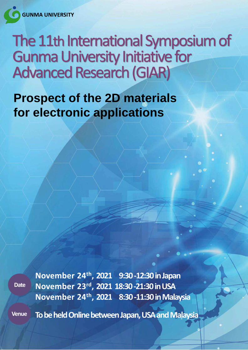
Date
November 24th, 2021 9:30 -12:30 in Japan
November 23rd, 2021 18:30 -21:30 in USA
November 24th, 2021 8:30 -11:30 in Malaysia
To be held Online betweenJapan, USA and Malaysia
Prospect of the 2D materials for electronic applications
Venue
The 11th International Symposium of Gunma University Initiative for Advanced Research (GIAR)
GUNMA UNIVERSITY

About GIAR
“Gunma University Initiative for Advanced Research (GIAR)” was established in 2014 to
aim at developing advanced research fields where the university has already great
strengths. As the first step, we developed programs for “Integrated Oncology Research”
and “Endocrinology, Metabolism and Signal Research”. We also launched international
open laboratories at GIAR with top-class overseas researchers to create global research
environment. GIAR pursues splendid discoveries for our society and will continue to
forge ahead toward our goal of becoming one of the world-leading research institutes.
In April 2019, GIAR was reorganized into three research divisions: “Integrated Oncology
Research”, “Endocrinology, Metabolism and Signal Research”, and “Element-Function
Chemistry”. Each division collaborates with the international open laboratories and
recruits competent young researchers from all over the world. Moreover, in October
2019, “Viral Vector Core” was newly established in GIAR to develop and supply cutting-
edge viral vectors as a core hub in this research area in Japan.

WELCOME ADDRESS
9:30 - 9:35 in JST Yasuki Ishizaki (President of Gunma University)
18:30 - 18:35 in CST
8:30 - 8:35 in MYT
TALK
9:35 - 10:20 in JST Two-Dimensional Neuromorphic Computing
18:35 - 19:20 in CST Materials and Devices
8:35 - 9:20 in MYT Mark C. Hersam (Northwestern University, USA)
10:20 - 11:05 in JST In-situ observation of surface chemical processes
19:20 - 20:05 in CST including hydrogen on 2D materials
9:20 - 10:05 in MYT Jun Yoshinobu (ISSP, The University of Tokyo, Japan)
11:05 - 11:50 in JST Development of Chemical Recognition Function
20:05 - 20:50 in CST for MoS2 Field-Effect-Transistor (FET) Sensor
10:05 - 10:50 in MYT Tadahiro Komeda (IMRAM, Tohoku University, Japan)
11:50 - 12:25 in JST Graphene FET for Biosensor Applications
20:50 - 21:25 in CST Ruslinda Binti A. Rahim (INEE, UniMAP, Malaysia)
10:50 - 11:25 in MYT
CLOSING REMARKS
12:25 - 12:30 in JST Minoru Hanaya
21:25 - 21:30 in CST (GIAR Director Vice President of Gunma University)
11:25 - 11:30 in MYT
Organizer: Md. Zakir Hossain (GIAR, Gunma University)

Mark C. Hersam, Ph.D.
Position: Walter P. Murphy Professor of Materials Science and Engineering
Affiliation: Northwestern University
e-mail address: [email protected]
Research Career
Mark C. Hersam is the Walter P. Murphy Professor of Materials Science and Engineering and Director of the Materials Research Center at Northwestern University. He also holds faculty appointments in the Departments of Chemistry, Applied Physics, Medicine, and Electrical Engineering. He earned a B.S. in Electrical Engineering from the University of Illinois at Urbana-Champaign (UIUC) in 1996, M.Phil. in Physics from the University of Cambridge (UK) in 1997, and a Ph.D. in Electrical Engineering from UIUC in 2000. His research interests include nanomaterials, nanomanufacturing, nanoelectronics, scanning probe microscopy, renewable energy, and quantum information science. Dr. Hersam has received several honors including the TMS Robert Lansing Hardy Award, U.S. Science Envoy Fellowship, MacArthur Fellowship, AVS Medard W. Welch Award, and eight Teacher of the Year Awards. An elected member of the National Academy of Inventors, Dr. Hersam has founded two companies, NanoIntegris and Volexion, which are commercial suppliers of nanoelectronic and battery materials, respectively. Dr. Hersam is a Fellow of MRS, ACS, AVS, APS, AAAS, SPIE, and IEEE, and also serves as an Associate Editor of ACS Nano.
Talk Title
Two-Dimensional Neuromorphic Computing Materials and Devices
Abstract
The exponentially improving performance of conventional digital computers has slowed in recent years due
to the speed and power consumption issues that are largely attributable to the von Neumann bottleneck
(i.e., the need to transfer data between spatially separate processor and memory blocks). In contrast,
neuromorphic (i.e., brain-like) computing aims to circumvent these limitations by spatially co-locating
processor and memory blocks or even combining logic and data storage functions within the same device.
In addition to reducing power consumption in conventional computing, neuromorphic devices provide
efficient architectures for emerging applications such as image recognition, machine learning, and artificial
intelligence. With this motivation in mind, this talk will explore the opportunities for two-dimensional
materials in neuromorphic devices. For example, by combining p-type black phosphorus with n-type
transition metal dichalcogenides, gate-tunable diodes have been realized, which show anti-ambipolar
transfer characteristics that are suitable for artificial neurons, competitive learning, and spiking circuits. In
addition, by exploiting field-driven defect motion mediated by grain boundaries in monolayer MoS2,
gate-tunable memristive phenomena have been achieved, which enable hybrid memristor/transistor
devices (i.e., ‘memtransistors’) that concurrently provide logic and data storage functions. The planar
geometry of memtransistors further allows multiple contacts to the channel region that mimic the behavior
of biological neurons such as heterosynaptic responses and continuous learning. Overall, this work
introduces new foundational circuit elements for neuromorphic computing in addition to providing
alternative pathways for studying and utilizing the unique quantum characteristics of two-dimensional
materials.

Jun Yoshinobu, Dr. Sci.
Position: Professor
Affiliation: The Institute for Solid State Physics, The University of Tokyo
e-mail address: [email protected]
Research Career
1989: Dr. of Science, Kyoto University
1989-1991: Postdoc, Pittsburgh Univ.
1991-1992: Postdoc. RIKEN
1991-1997: Researcher, RIKEN
1997-2007: Assoc. Prof., ISSP, Univ. of Tokyo
2007- present: Prof., ISSP, Univ. of Tokyo
Talk Title
In-situ observation of surface chemical processes including hydrogen on 2D materials
Abstract
There has been a growing interest in the functionalities and reactions on two-dimensional materials
including graphene and transition-metal dichalcogenides (TMDs). In this talk, I will present two topics from
our recent research activities.
(1) Scalable and rapid production of graphene is required for its industrial applications. Chemical vapor
deposition (CVD) is one of the promising methods to synthesize large-area single-crystalline graphene. In a
typical CVD process of graphene, gaseous CH4 with Ar and H2 is supplied onto a Cu substrate at a
temperature of about 1000 °C, where CH4 molecules are decomposed to form the nucleus of graphene.
Here, we used radiation-mode optical microscopy (Rad-OM), which can visualize graphene growth in real
time by utilizing the difference in the emissivity between graphene and Cu. Furthermore, we combined the
Rad-OM with in-situ synchrotron radiation XPS (SR-XPS) to characterize surface species and elucidate the
effect of hydrogen.
(2) Molybdenum disulfide (MoS2) is one of the TMDs and has a layered structure. Monolayer or a few layer
MoS2 is expected to have various applications such as field-effect-transistors, optoelectronic devices, and gas
sensors. On the other hand, MoS₂ has been used as catalysts for many years. In this work, we have
investigated the interaction of molecular hydrogen on the Pd/MoS2 surface using ambient-pressure (AP) XPS
under hydrogen atmosphere. Comparing the case of an inert MoS2 bare surface, we found that the
Pd-deposited MoS2 basal surface has higher activity for the dissociation of hydrogen molecules. Based on
the XPS results, we confirmed that the active site for dissociation of molecular hydrogen is ascribed to
deposited Pd atoms, and the electronic states of the MoS2 substrate have been modulated by hydrogen
atoms spilled over onto the MoS2 surface.

Tadahiro Komeda, Ph.D.
Position: Professor
Affiliation: Institute of Multidisciplinary Research for Advanced Materials
(IMRAM), Tohoku University
e-mail address: [email protected]
Research Career
Tadahiro Komeda received a bachelor’s degree and a PhD from Kyoto University, Japan. His thesis theme is
the angle resolved photoemission spectroscopy for adsorbed molecules on metal surfaces. He was a
post-doctoral fellow with Prof. John H. Weaver at University of Minnesota. After working as a research staff
in Texas Instruments, he jointed Riken, Japan, starting low temperature STM for the studies of 'nano
chemistry' using tunneling electrons. He joined Tohoku University as a full professor at 2003. His research
group works on developing chemical-analysis techniques for molecular electronic and spintronic device
materials to enable a single molecule characterization using scanning probe microscopes.
Talk Title
Development of Chemical Recognition Function for MoS2 Field-Effect-Transistor (FET) Sensor
Abstract
Miniaturized sensor,that is suitable to operate with an in vivo condition, has attracted great demand for past
decades. For such an application field-effect-transistor (FET) sensor with using the atomically thin MoS2
channel material can be a promising candidate. Due to the atomic thin layer, MoS2 channel can be more
sensitive to the adsorption of different organic molecules when it is used in FET. Molecular identification
using FET devices has been performed by the drain current change that can be attributed to the charge
exchange or the polarization of molecules. This technique however has no significant chemical sensitivity to
the molecules. In this talk, utilizing the MoS2-FET devices, molecule sensor has been developed that has the
chemical recognition capability. Visible light was injected onto the deposited channel and molecular
identification was observed by the electronic property of the FET. In addition, π-electron molecules that
have the broad band photo response properties such as phthalocyanine, methylene blue, di-carbocyanine
iodide and many more organic molecules were used as adsorbates for MoS2 channel and detected by light
injection.

Ruslinda A.Rahim, Ph.D.
Position: Director of National Nanotechnology Centre / Research Fellow
Affiliation: National Nanotechnology Centre (NNC),
Ministry of Science Technology and Innovation Institute
of Nano Electronic Engineering (INEE),
Universiti Malaysia Perlis (UniMAP)
e-mail address: [email protected] / [email protected]
Research Career
Ruslinda binti A. Rahim received the Doctor of Philosophy (Ph.D) majoring in Nanoscience and Nanoengineering from Waseda University, Japan in September 2012. She also received M. Eng and B. Eng degree in Electrical and Electronic Engineering from Muroran Institute of Technology, Japan in 2007 and 2002, respectively. Currently, she is a Director of National Nanotechnology Centre under Ministry of Science, Technology and Innovation (MOSTI). She also a Research Fellow in Institute of Nano Electronic Engineering (INEE), Universiti Malaysia Perlis (UniMAP) and Associate Research Fellow in Institute of Microengineering and Nanoelectronics (IMEN), The National University of Malaysia (UKM). Her research interests include Nanoelectronics, Nanostructure device, Biosensors, Bioelectronics, DNA and protein detection, Aptamer and surface chemistry on carbon-based materials. She also active in several societies such as a Board of Engineers Malaysia, Professional Technologist Malaysia (MBOT) (Nanotechnology), Committee member of Malaysia Nanotechnology Association, Board of Member Malaysia Sensor Society and Editor of the International Journal of Nanoelectronics and Materials.
Talk Title
Graphene FET for Biosensor Applications
Abstract
Field-effect transistors (FETs) have succeeded in modern electronics in an era of computers and hand-held
applications. Currently, considerable attention has been paid to direct electrical measurements, which work
by monitoring changes in intrinsic electrical properties. Further, FET-based sensing systems drastically reduce
cost, mass production capability, fast-result and ease down-stream applications such as biosensor.
Graphene is a unique two-dimensional material with its spectacular structural and electronic properties that
has appealed towards the sensing material due to its high electron mobility, transparency and mechanical
strength. In this work, current technologies for sensing applications is presented specifically focus on
high-performance FET-based sensor integration with nano-sized materials, which requires understanding
the interaction of surface materials with the surrounding environment.

Gunma University Initiative for Advanced Research (GIAR)
https://www.giar.gunma-u.ac.jp/en/