hard xray diagnostic for lower hybrid current drive on
TRANSCRIPT

Hard Xray Diagnostic for Lower Hybrid Current Drive on Alcator C-
Mod
J. Liptac, J. Decker, R. Parker, V. Tang, P. Bonoli MIT PSFC Y. Peysson CEA Cadarache
APS 2003 Albuquerque, NM

Abstract
•A Lower Hybrid Current Drive (LHCD) system is being installed on C-Mod allowing the exploration of advanced tokamak (AT) regimes through current profile control
•The LH current profile may be inferred through non-thermal Bremsstrahlung emission measured by a pinhole camera
•A Fokker-Planck (FP) model coupled to camera data gives information about the LH modified electron distribution function
•Camera design and FP model will be discussed

LH Waves
LHCD works through electron Landau damping around v~3vth
LHCD is calculated based on•Ray tracing•Imaginary part of the hot plasma dispersion relation or an FP solver•k|| =(krBr+m/rBθ+n/RBφ)/|B|
•Creation of non-thermal Bremsstrahlung radiation from high energy tail
Experimental verification of LHCD location is needed
Bonoli ACCOME Simulation
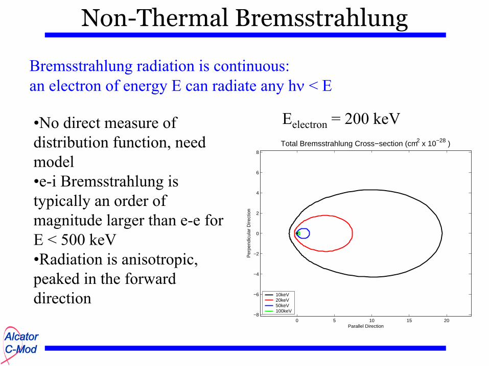
Non-Thermal Bremsstrahlung
Bremsstrahlung radiation is continuous: an electron of energy E can radiate any hν < E
•No direct measure of distribution function, need model•e-i Bremsstrahlung is typically an order of magnitude larger than e-e for E < 500 keV•Radiation is anisotropic, peaked in the forward direction
0 5 10 15 20−8
−6
−4
−2
0
2
4
6
8
Total Bremsstrahlung Cross−section (cm2 x 10−28 )
Parallel Direction
Per
pend
icul
ar D
irect
ion
10keV20keV50keV100keV
Eelectron = 200 keV

A
B
C
D
E
K
J
G
F
H
Experimental Layout
LH AntennaKlystrons
HXRDiagnostic
Wave Guides
C-Mod top view
•Located on mezzanine•12 klystrons at 250kW each → 3MW•f = 4.6GHz
•Located on C-port•Grill composed of 96 waveguides, 4 rows of 24•Dynamic phase change possible, ~ms, allowing for pre-program spectra or feedback control
•Located on B-port•32 channel pinhole camera•20-250keV energy range•~1.5cm spatial resolution•~10ms temporal resolution
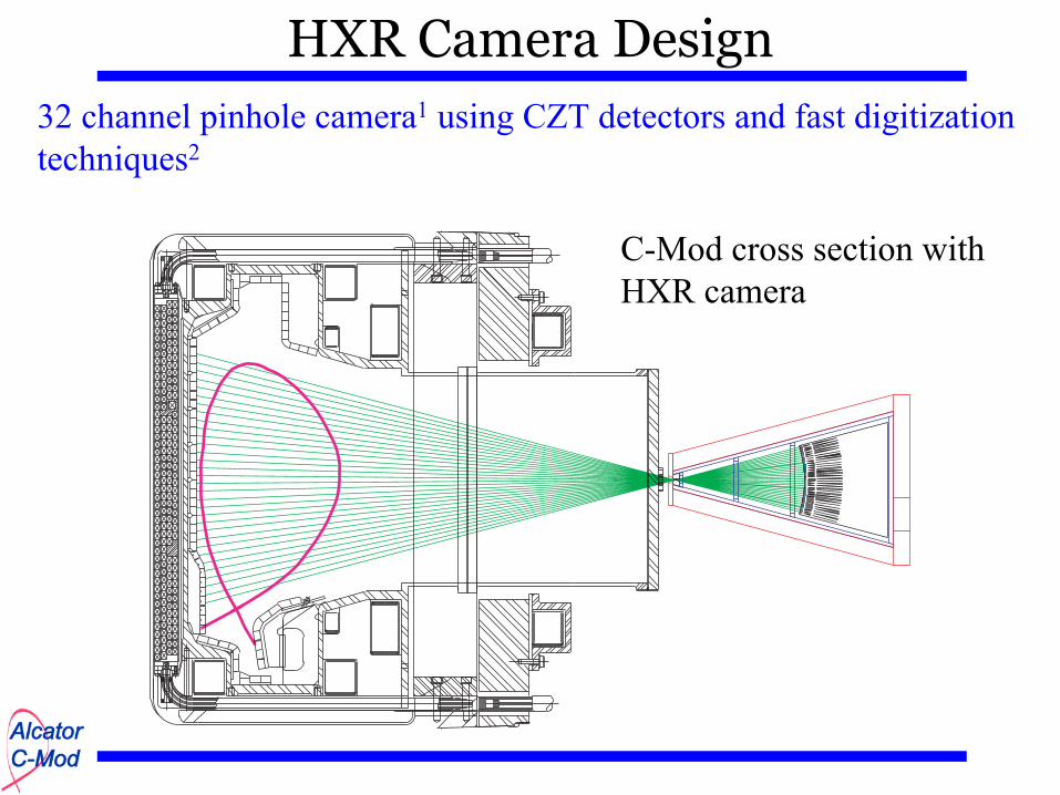
HXR Camera Design32 channel pinhole camera1 using CZT detectors and fast digitization techniques2
C-Mod cross section with HXR camera

HXR Camera Design (cont.)CdZnTe detectors:
•Flexibility through software data analysis•Energy resolution limited by detector•Improved noise rejection/pile up detection•Lower system cost•Possibility of real time feedback control of n||
Fast digitization allows:
Data management:
•High Z 49.1, high density 5.8g/cm3 •No cooling or magnetic shielding•Made in the USA- eV Products
•Up to 2GB/shot raw data•~150 shot scratch disk•Local data processing•Processed data archived
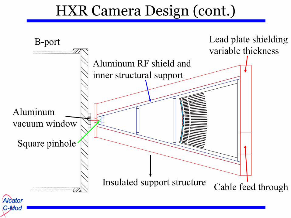
HXR Camera Design (cont.)
Aluminum RF shield and inner structural support
Lead plate shielding variable thickness
Square pinhole
Insulated support structure Cable feed through
Aluminum vacuum window
B-port

Pulse Processing
Preamplifier
Photons
Detector Amplifierand
Shaper
FastDigitizer
0 0.2 0.4 0.6 0.8 1 1.2 1.4 1.6 1.8 20
5
10
15
20
25
30
35
40Detector Current vs Time
Time (µs)
Cu
rren
t (n
A)
Ie
Ih
0 0.5 1 1.5 2 2.5 3 3.5 40
0.5
1
1.5
2
2.5
3
3.5
4
4.5
5Preamp Voltage vs Time
Time (µs)
Vo
ltag
e (m
V)
0 0.2 0.4 0.6 0.8 1 1.2 1.4 1.6 1.8 20
0.1
0.2
0.3
0.4
0.5
0.6
0.7
0.8
0.9
1Gaussian Shaper Output
Time (µs)
Vo
ltag
e (V
)
•Energy resolution better than 10% at 60kev•Charge transport limits count rates to ~1MHz
•High sensitivity ~120mV/MeV•τf =1ms•Small size 2.6×1.5cm
•Developed in house•~1µs pulse width•DC offset•Line driver•Small size 2.5×7.6cm
DTACQ ACQ216
•CPCI form factor•16ch/board at 10MHz•1GB/board memory•14 bit resolution
eV Products 5×5×2mm CZT
eV Products eV-5093 Preamp
Gaussian Shaper

Shaping Electronics
•No undershoot → better energy performance at high count rate•Easy to fit → reduces pile up and improves rejection
Time (us)
0 0.5 1.0 1.5 2.00
100
200
300
400
Volt
age
(mV
)
Vdiff
V1
V2
V3
Gaussian pulse shape3:
Shaper step response from PSPICE model

+5
DC_LD
-5
+5 +5
-5-5 -5
+5
PRE_IN
-5
V_OFF
+5
DC_LD
OUT
C30 0.01uF
C31 6.8uF
C38
0.1uF
U2
LMH6702/SOT23_5
3
4
52
1
+
-
V+
V-
OUT
R15
23.7
U1
LMH6702/SOT23_5
3
4
52
1
+
-
V+
V-
OUT
R22 237
U4
LMH6702/SOT23_5
3
4
52
1
+
-
V+
V-
OUT
R4 10
R23 237
R17
237
C23
270pF
R1 10
C20
3300pF
C7 6.8uF
U5
LMH6702/SOT23_5
3
4
52
1
+
-
V+
V-
OUT
R13 237R11 237
C5 470pF
C13 0.01uF
C4 330pF
C15
0.1uF
C16
0.1uF
C34 6.8uF
C35 6.8uF
C9 6.8uF
C40 6.8uF
C6 6.8uF
R21
1KC39 0.01uF
C32 6.8uF
C2 180pF
C3 330pF
R5 90.9R3 137
U3
LMH6702/SOT23_5
3
4
52
1
+
-
V+
V-
OUTC17
0.1uF
R24
23.7
C29 0.01uFC27 0.01uF
R19 10
R14 237
C26
470pF
R9 365R2 90.9
C25
180pF
R8 90.9
C14
1800pF
C12 0.01uF
C28 0.01uF
C22
330pF
C18
0.1uFC21
3300pF
R7 10
R12 237
Q1MMB3904
C8 6.8uF
C37
3300pF
C11 0.01uF
R18
237
C36 0.01uF
R6 267
C19
3300pF
R10
49.9
C1 270pF
R16
237
C33 6.8uF
R20 49.9
C24
330pF
C10 0.01uF
Vdiff
V1 V2V3
Shaping Electronics (cont.)
Gaussian shaper realized through Sallen-Key filter and surface mount PCB
•Flexible gain and pulse width•DC offset used to adjust signal into digitizer range of ± 2.5V•50Ω line driver

0 0.2 0.4 0.6 0.8 1-2
0
2
4
6
8
10
12
14Current Profiles
Normalized Radius (r/a)
Cur
rent
Den
sity
(M
A/m
2 )
Total 804 kALH 390 kAOH -27.7 kABS 434 kA
0 0.2 0.4 0.6 0.8 10
1
2
3
4Density Profile
Normalized Radius (r/a)
Ele
ctro
n D
ensi
ty (
1020
/m3 )
0 0.2 0.4 0.6 0.8 10
2
4
6
8
10q Profile
Normalized Radius (r/a)
Saf
ety
Fac
tor
0 0.2 0.4 0.6 0.8 10
2
4
6
8Temperature Profiles
Normalized Radius (r/a)
Tem
pera
ture
(ke
V)
Te
Ti
Count RateCount rate estimated through AT target plasma parameters and a crude average over the emissive region
∑∑ ∆∆=k i
ikdc
e lhhrjdaanN νν ),(2
222
.Count Rate:
ac = collimator sizead = detector sized = pinhole to detector spacing

Count Rate (cont.)
0 50 100 150 200 250 30010
0
101
102
103
104
105
106 Count Rate vs Energy
Energy (keV)C
ount
Rat
e (1
/s)
•Spatial resolution linked to count rate through aperture size•∆hν is set by bin size, or detector resolution•Larger energy bins increase the number of counts per channel at the expense ∆hν•Temporal resolution determined by statistical accuracy needed
Spatial, temporal, and energy resolution are interdependent through counting statistics

30 35 40 45 50 55 60 65 70 75 8010
3
104
105
106
Pinhole to Detector Spacing (cm)
Co
un
t R
ate
(1/s
)
Count Rate and Resolution vs Pinhole to Detector Spacing
E=20-250 keV
E=35-250 keV
E=50-250 keV
30 35 40 45 50 55 60 65 70 75 801.2
1.4
1.6
1.8
2
2.2
2.4
2.6
2.8
Res
olu
tio
n (
cm)
ac=0.5cm
Spatial Resolution
0.1 0.2 0.3 0.4 0.5 0.6 0.7 0.8 0.9 110
3
104
105
106
Aperture size (cm)
Count
Rat
e (1
/s)
Count Rate and Resolution vs Aperture Size
E=20-250 keV
E=35-250 keV
E=50-250 keV
0.1 0.2 0.3 0.4 0.5 0.6 0.7 0.8 0.9 10
0.5
1
1.5
2
2.5
3
3.5
4
4.5
Res
olu
tion (
cm)
Resolution Mapping Resolution Mapping
ac=0.5cm
d=39cm
Spatial resolution:Estimation: ∆r ~ 2a / #chords=1.4cmGeometry: ∆r = (1 + D/d)ac ~ 1.7cm
Plasma
D d
ac
ad
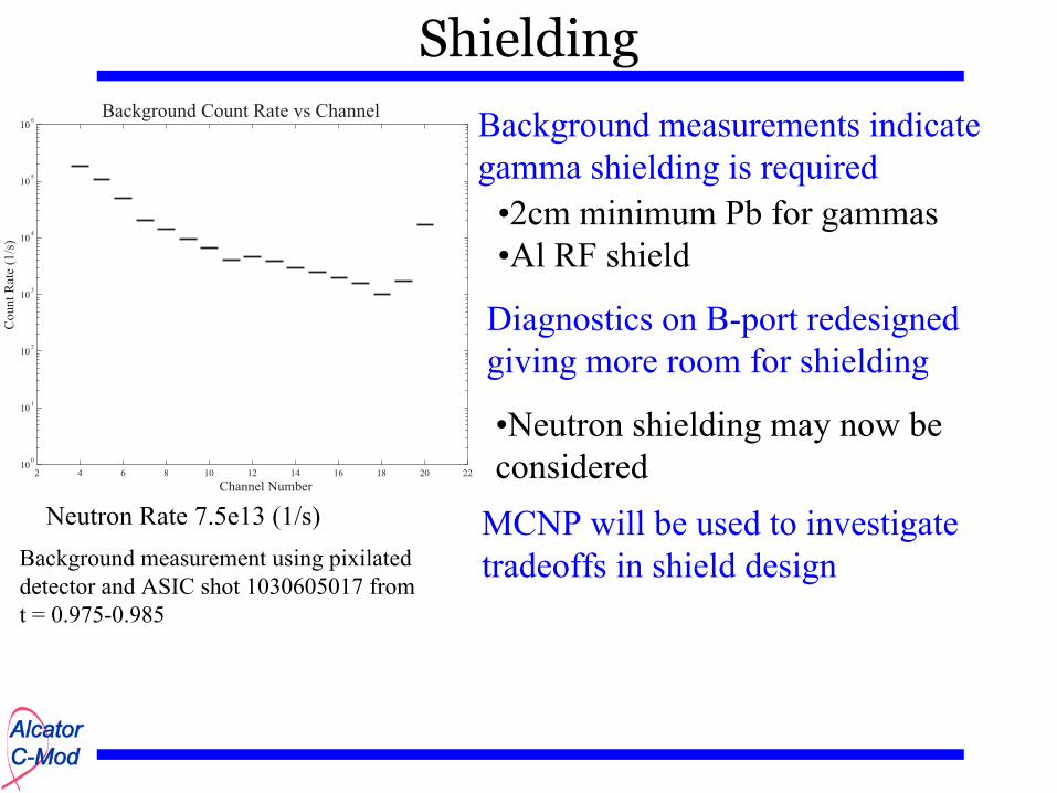
Shielding
Diagnostics on B-port redesigned giving more room for shielding
2 4 6 8 10 12 14 16 18 20 2210
0
101
102
103
104
105
106
Background Count Rate vs Channel
Channel Number
Count
Rat
e (1
/s)
Background measurements indicate gamma shielding is required
•2cm minimum Pb for gammas•Al RF shield
•Neutron shielding may now be considered
Background measurement using pixilated detector and ASIC shot 1030605017 from t = 0.975-0.985
MCNP will be used to investigate tradeoffs in shield design
Neutron Rate 7.5e13 (1/s)
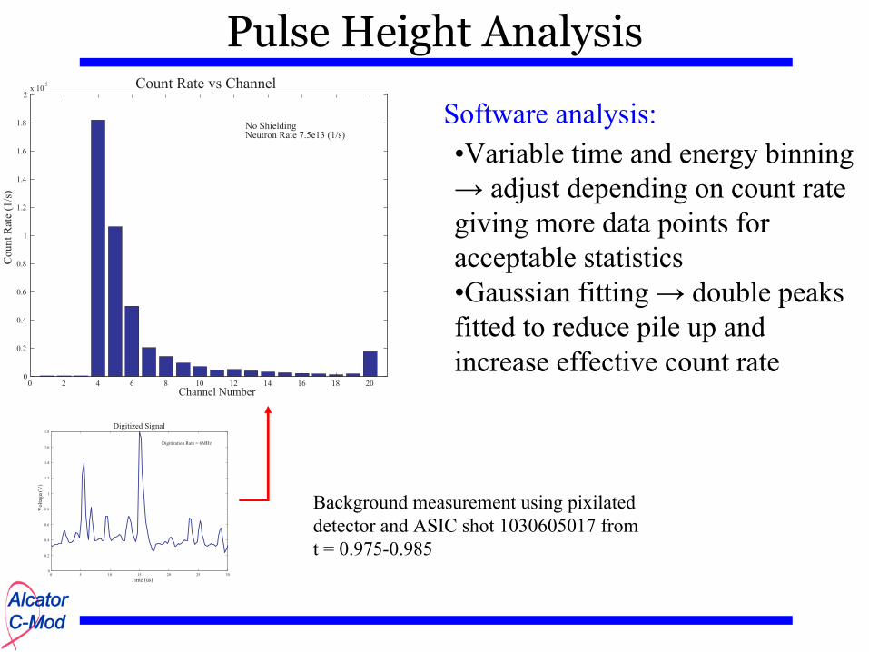
Pulse Height Analysis
0 2 4 6 8 10 12 14 16 18 200
0.2
0.4
0.6
0.8
1
1.2
1.4
1.6
1.8
2x 10
5 Count Rate vs Channel
Channel Number
Count
Rat
e (1
/s)
No ShieldingNeutron Rate 7.5e13 (1/s)
Software analysis:•Variable time and energy binning → adjust depending on count rate giving more data points for acceptable statistics•Gaussian fitting → double peaks fitted to reduce pile up and increase effective count rate
Background measurement using pixilated detector and ASIC shot 1030605017 from t = 0.975-0.985
0 5 10 15 20 25 300
0.2
0.4
0.6
0.8
1
1.2
1.4
1.6
1.8
Digitized Signal
Time (us)
Volt
age
(V)
)
Digitization Rate = 6MHz

Reconstruction
•MATLAB GUI developed for Tore Supra HXR analysis is being adapted for C-Mod
HXR measures the line integrated emissivity and a reconstruction4
is needed to recover the radial profile
Reconstruction methods include:•Abel inversion•Minimum Fisher•Maximum entropy•And others

Distribution Function Model
-5 0 5 10 15
-2
0
2
4
6
8
10
12
14
16
ppar/pth-ref
pper
p/pt
h-re
f
2-D steady state electron distribution function
FPCode
Local plasma parametersT, n, Ip, Zeff
LH parametersDql, vmin, vmax
fe(p||,p⊥)
Code written by J. Decker and Y. Peysson
Physical interpretation•Dql → LH power level
•vmax → Wave accessibility
•vmin → Landau damping
LH distribution function model5 coupled with a FP calculation gets at the underlying physics while including collision and the Ohmic field
LH model
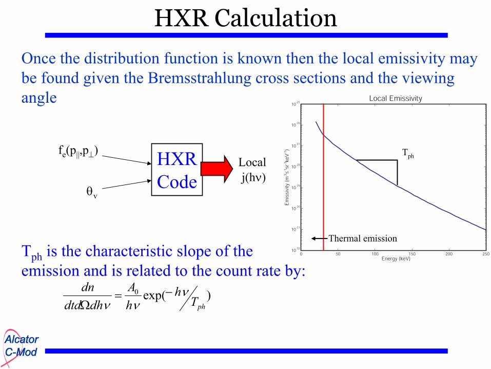
0 50 100 150 200 25010
-32
10-31
10-30
10-29
10-28
10-27
10-26
10-25
Local Emissivity
Energy (keV)
Em
issi
vity
(m
3 s-1 s
r-1 keV
-1)
HXR Calculation
Thermal emission
Tphfe(p||,p⊥) HXR
Code
Once the distribution function is known then the local emissivity may be found given the Bremsstrahlung cross sections and the viewingangle
θv
Local j(hν)
)exp(0
phTh
hA
dhdtddn ν
νν−=
Ω
Tph is the characteristic slope of the emission and is related to the count rate by:
Summary
•A 32 channel CZT detector pinhole camera using fast digitization has been developed to measure the 20-250keV electron population resulting from LHCD
•Emissivity profile reconstruction gives the LHCD location
•Measurements coupled to a FP model give information about the electron distribution function and are directly related to wave accessibility and power level
•Camera will be ready for operation when LH is installed
References
1 Y. Peysson and F. Imbeaux Rev. Sci. Instrum. 70(10) 3987 (1999)
2 R. O’Connell et. al. Rev. Sci. Instrum. 74(3) 2001 (2003)
3 Ohkawa et. al. Nuc. Instrum. Meth. 138 85 (1976)
5J. Decker and Y. Peysson 29th EPS Montreax 26B(P-4.052) (2002)
4 Anton et. al. Plasma Phys. Control. Fusion 38 1849 (1976)