hardware design fundamentals - purdue engineering · pdf filehardware design fundamentals...
TRANSCRIPT
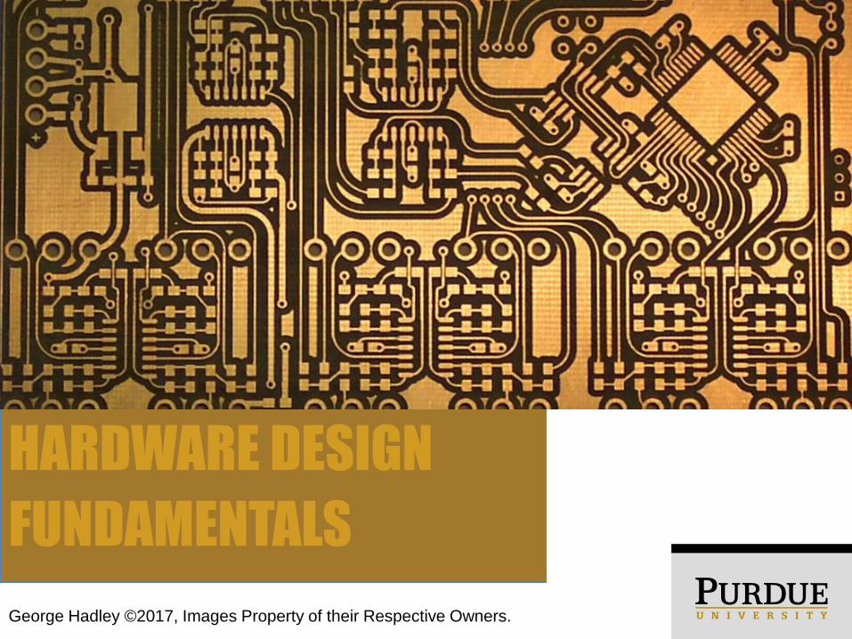
HARDWARE DESIGN
FUNDAMENTALS
George Hadley ©2017, Images Property of their Respective Owners.

OUTLINE• PCB Design Objective
• PCB Manufacturing Process
• Design Automation Tools
• The Design Process
• Parts
• Schematics
• Layouts
• DRC and Toolfile Generation
• Ordering Circuit Boards
• Miscellaneous PCB Topics

OBJECTIVE
• Q: What’s the “goal” of the hardware design
process?
• A: Well-designed circuit boards that connect
electrical components while meeting electrical
requirements (signal integrity, power, etc.)

PCB MANUFACTURING PROCESSOverview
• The printed circuit board (PCB) manufacturing process
contains a number of steps:
1. Base Materials
2. Etching
3. Hole/via Drilling
4. Through-hole plating
5. Solder mask application
6. Silkscreen application
7. Electrical testing

PCB MANUFACTURING PROCESSBase Materials
• To make a (simple) circuit board, require:
• PCB Blank: Substrate board (typically FR4) with copper
laminated on both sides
• Resist: A material which protects the copper on the
board from the etchant
• Etchant: A chemical solution used to dissolve copper on
the circuit board
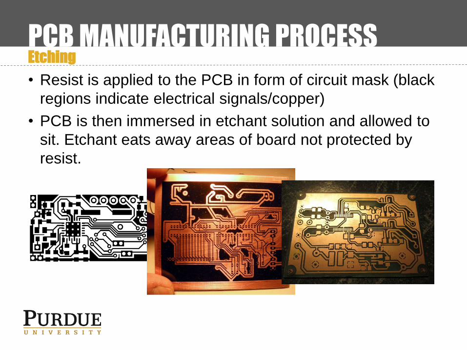
PCB MANUFACTURING PROCESSEtching
• Resist is applied to the PCB in form of circuit mask (black
regions indicate electrical signals/copper)
• PCB is then immersed in etchant solution and allowed to
sit. Etchant eats away areas of board not protected by
resist.

PCB MANUFACTURING PROCESSDrilling/Plating
• A drill with fine-diameter bits is used for drilling holes
• Holes used to connect signals between layers of the
board are known as vias (also used for heat transfer)
• To ensure electrical connection is made (even if drill isn’t
precise), vias possess ring of copper known as an
annular ring
• Once drilled, vias
are electroplated
to ensure
conductive path
between board
layers
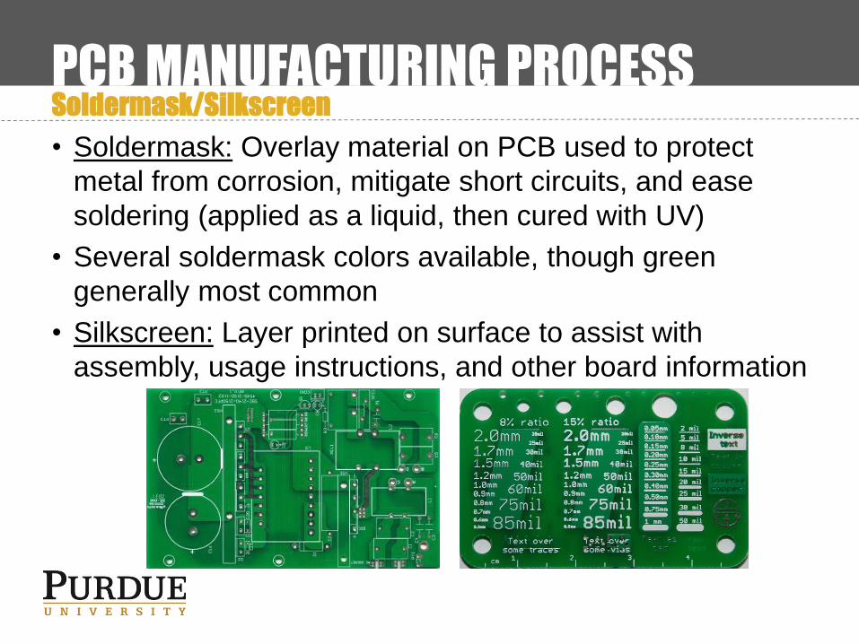
PCB MANUFACTURING PROCESSSoldermask/Silkscreen
• Soldermask: Overlay material on PCB used to protect
metal from corrosion, mitigate short circuits, and ease
soldering (applied as a liquid, then cured with UV)
• Several soldermask colors available, though green
generally most common
• Silkscreen: Layer printed on surface to assist with
assembly, usage instructions, and other board information

PCB MANUFACTURING PROCESSElectrical Testing
• Once finished, boards are subjected to electrical tests to
ensure electrical connectivity across boards and that the
boards were manufactured correctly
• In spite of such tests, students should carefully visually
inspect boards upon reception to check for defects

DESIGN AUTOMATION TOOLSList of EDA Tool Suites
• Many Electronic Design Automation (EDA) tool suites are
available for circuit board design and simulation, such as:
• Eagle: Easy-to-use, easy to learn, large hobbyist
community
https://www.autodesk.com/products/eagle/overview
• Altium: Simulation and advanced features, more
professional, expensive http://www.altium.com/
• KiCAD: Unrestricted free and open source software,
used by CERN http://www.kicad-pcb.org/
• OrCAD, Allegro, PADS, etc.: Other proprietary suites
used in industry

THE DESIGN PROCESSParts
• In EDA suites such as Eagle, a part is an object which
represents an electronic component used in a circuit
board. Parts form associations between various views:
• Symbol: A schematic representation of the component,
featuring pins and pin names
• Footprint: A PCB layout representation of the
component, featuring dimensions on board, as well as
various layers (copper, silkscreen, documentation, etc.)
used in the final PCB
• Part libraries are available in Eagle and online, or users
can create their own parts (see tutorial)

THE DESIGN PROCESSParts – Tips and Tricks
• Many ICs (especially microcontrollers) multiplex many
functions onto each pin. Choose only those functions
called for in your application to avoid schematic clutter
• Many ICs have multiple pins which have the same name
(VCC, GND, NC, etc.). Use
<Name>@n (n=1, 2, 3…) to
have pins with unique names
which display the same in
schematic view (Eagle only)

THE DESIGN PROCESSSchematics
• Schematic: a symbolic representation of a circuit
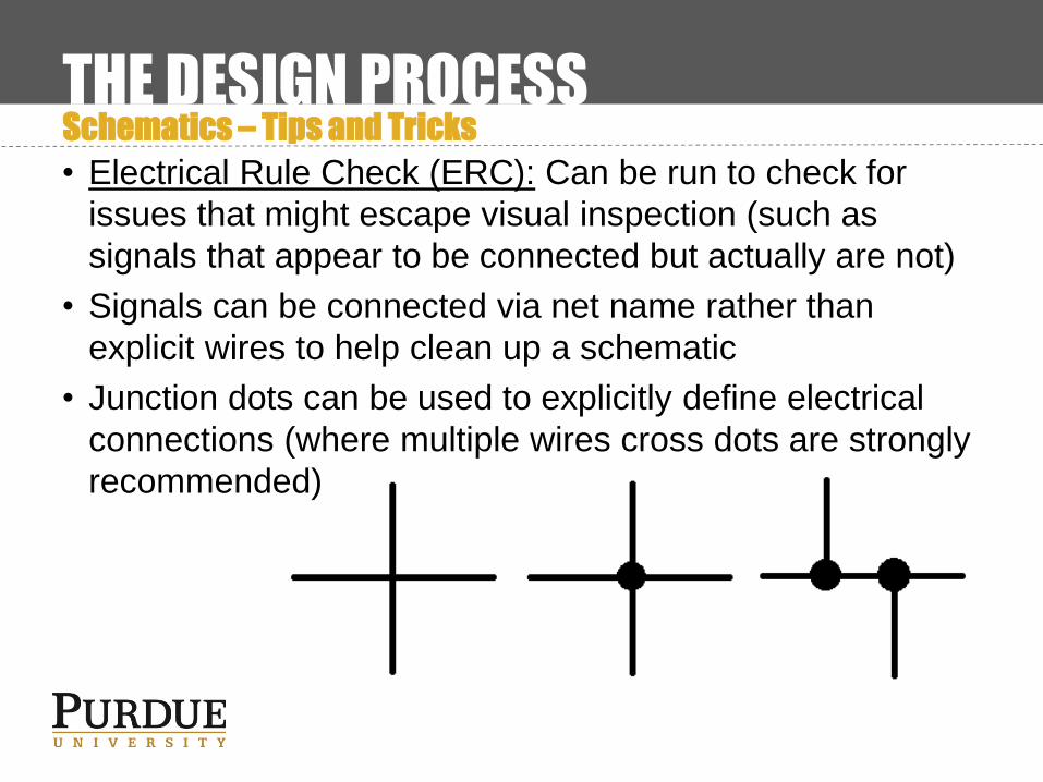
THE DESIGN PROCESSSchematics – Tips and Tricks
• Electrical Rule Check (ERC): Can be run to check for
issues that might escape visual inspection (such as
signals that appear to be connected but actually are not)
• Signals can be connected via net name rather than
explicit wires to help clean up a schematic
• Junction dots can be used to explicitly define electrical
connections (where multiple wires cross dots are strongly
recommended)

THE DESIGN PROCESSLayouts
• Layout: an electrical representation of a circuit board
corresponding to the design of the finished board
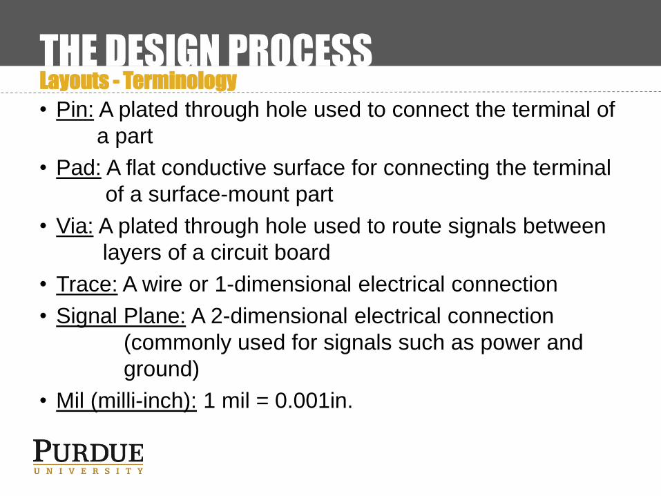
THE DESIGN PROCESSLayouts - Terminology
• Pin: A plated through hole used to connect the terminal of
a part
• Pad: A flat conductive surface for connecting the terminal
of a surface-mount part
• Via: A plated through hole used to route signals between
layers of a circuit board
• Trace: A wire or 1-dimensional electrical connection
• Signal Plane: A 2-dimensional electrical connection
(commonly used for signals such as power and
ground)
• Mil (milli-inch): 1 mil = 0.001in.
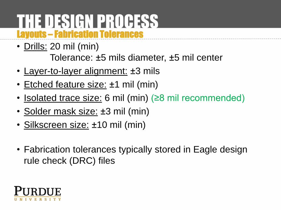
THE DESIGN PROCESSLayouts – Fabrication Tolerances
• Drills: 20 mil (min)
Tolerance: ±5 mils diameter, ±5 mil center
• Layer-to-layer alignment: ±3 mils
• Etched feature size: ±1 mil (min)
• Isolated trace size: 6 mil (min) (≥8 mil recommended)
• Solder mask size: ±3 mil (min)
• Silkscreen size: ±10 mil (min)
• Fabrication tolerances typically stored in Eagle design
rule check (DRC) files

THE DESIGN PROCESSLayouts – General Layout Guidelines
• Recommended trace/space: 10-16mil (general)
• Power and ground traces should be sized for current
being passed (trace width current capacity charts
available online)
• Follow all manufacturer PCB layout recommendations
• Decoupling capacitors should be placed as close to
associated ICs as possible
• Provide space and mechanical support for connectors,
heat sinks, and standoffs
• Incorporate headers or vias for verification and debugging

THE DESIGN PROCESSDesign Rule Check (DRC) and Tool File Generation
• Once a layout has been completed, it must be checked to
ensure it can be manufactured by the board house. This
is done by running a Design Rule Check (DRC)
• Once a design has been refined and passes DRC, a
software tool (CAM processor, in the case of Eagle) must
be run to generate the files used by the board house tools
to assemble the boards.
• The industry standard for PCB tool files is the Gerber
standard (RS-274-X). One file is produced for each layer
of the board (top/bottom copper, top/bottom silkscreen,
top/bottom soldermask, drills, etc.). Gerber files can be
viewed using a Gerber viewer

THE DESIGN PROCESSOrdering Circuit Boards
• Gerber files necessary to produce a board are
compressed into a zip archive, and sent out to a PCB
service. Some popular PCB services:
• Advanced Circuits: Fast turnaround times, US-based,
ITAR http://www.4pcb.com/4pcb-monthly-specials.html
• OSH Park: PCB panelization service, 3 board copies
per design submitted, US-based https://oshpark.com/
• Seeed Studio: Low cost, China-based, longer lead
times (~4 weeks), other services available (3D printing,
laser cutting, stencils, etc.) http://www.seeedstudio.com/
• Various PCB services can be compared at
http://pcbshopper.com
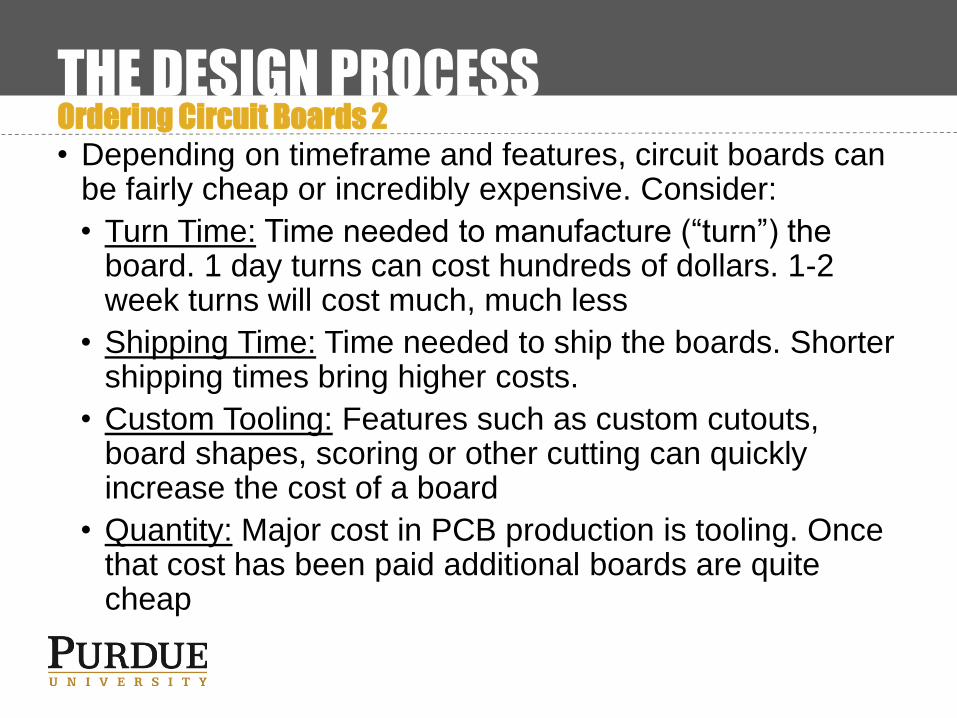
THE DESIGN PROCESSOrdering Circuit Boards 2
• Depending on timeframe and features, circuit boards can be fairly cheap or incredibly expensive. Consider:
• Turn Time: Time needed to manufacture (“turn”) the board. 1 day turns can cost hundreds of dollars. 1-2 week turns will cost much, much less
• Shipping Time: Time needed to ship the boards. Shorter shipping times bring higher costs.
• Custom Tooling: Features such as custom cutouts, board shapes, scoring or other cutting can quickly increase the cost of a board
• Quantity: Major cost in PCB production is tooling. Once that cost has been paid additional boards are quite cheap

Questions?