hardware development guide for the i.mx 6ultralite ... · mmdc io names are for the ddr3 default....
TRANSCRIPT
NXP SemiconductorsUser’s Guide
© 2015-2017 NXP B.V.
1 About this book
1.1 Overview
This document’s purpose is to help hardware engineers design and test their i.MX 6UltraLite processor-based designs. It provides information on board layout recommendations, and design checklists to ensure first-pass success and avoidance of board bring-up problems. It also provides information on board-level testing and simulation such as using BSDL (Boundary Scan Description Language) for board-level testing, using the IBIS model for electrical integrity simulation and more.
Engineers are expected to have a working understanding of board layouts and terminology, IBIS modeling, BSDL testing and common board hardware terminology.
This guide is released along with relevant device-specific hardware documentation such as datasheets, reference manuals and application notes available on www.nxp.com.
Document Number: IMX6ULHDGRev. 2, 10/2017
Contents1. About This Book . . . . . . . . . . . . . . . . . . . . . . . . . . . . . 12. i.MX 6UL Design Checklist . . . . . . . . . . . . . . . . . . . . 63. i.MX 6 Series Layout Recommendations . . . . . . . . . 164. Avoiding board bring-up problems . . . . . . . . . . . . . . 325. Understanding the IBIS model . . . . . . . . . . . . . . . . . 366. Using the manufacturing tool . . . . . . . . . . . . . . . . . . 467. Using BSDL for board-level testing . . . . . . . . . . . . . 518. Revision history . . . . . . . . . . . . . . . . . . . . . . . . . . . . 53A. Development Platforms . . . . . . . . . . . . . . . . . . . . . . 54
Hardware Development Guide for the i.MX 6UltraLite Applications Processor
Hardware Development Guide for the i.MX 6UltraLite Applications Processor, Rev. 2, 10/2017
2 NXP Semiconductors
About this book
1.1.1 Devices supported
This guide currently supports the i.MX 6UltraLite.
1.2 Essential reference
This guide is intended as a companion to the i.MX 6UltraLite chip reference manuals and data sheets. For reflow profile and thermal limits during soldering, see application note AN3300. These documents are available on www.nxp.com.
1.3 Suggested reading
This section lists additional reading that provides background for the information in this manual as well as general information about the architecture.
1.3.1 General Information
The following documentation provides useful information about the ARM processor architecture and computer architecture in general:
For information about the ARM Cortex-A7 processor see:
www.arm.com/products/processors/cortex-a/cortex-a7.php
• Computer Architecture: A Quantitative Approach (Fourth Edition) - by John L. Hennessy and David A. Patterson
• Computer Organization and Design: The Hardware/Software Interface (Second Edition), by David A. Patterson and John L. Hennessy
The following documentation provides useful information about high-speed board design:
• Right the First Time- A Practical Handbook on High Speed PCB and System Design - Volumes I & II - Lee W. Ritchey (Speeding Edge) - ISBN 0-9741936- 0-72
• Signal and Power Integrity Simplified (2nd Edition) - Eric Bogatin (Prentice Hall)- ISBN 0-13-703502-0
• High Speed Digital Design- A Handbook of Black Magic - Howard W. Johnson & Martin Graham (Prentice Hall) - ISBN 0-13-395724-1
• High Speed Signal Propagation- Advanced Black Magic - Howard W. Johnson & Martin Graham - (Prentice Hall) - ISBN 0-13-084408-X
• High Speed Digital System Design- A handbook of Interconnect Theory and Practice - Hall, Hall and McCall (Wiley Interscience 2000) - ISBN 0-36090-2
• Signal Integrity Issues and Printed Circuit Design - Doug Brooks (Prentice Hall) ISBN 0-13-141884-X
• PCB Design for Real-World EMI Control - Bruce R. Archambeault (Kluwer Academic Publishers Group) - ISBN 1-4020-7130-2
• Digital Design for Interference Specifications- A Practical Handbook for EMI Suppression -David L. Terrell & R. Kenneth Keenan (Newnes Publishing) - ISBN 0-7506-7282-X
Hardware Development Guide for the i.MX 6UltraLite Applications Processor, Rev. 2, 10/2017
NXP Semiconductors 3
About this book
• Electromagnetic Compatibility Engineering- Henry Ott (1st Edition - John Wiley and Sons) - ISBN 0-471-85068-3
• Introduction to Electromagnetic Compatibility - Clayton R. Paul (John Wiley and Sons) - ISBN 978-0-470-18930-6
• Grounding & Shielding Techniques - Ralph Morrison (5th Edition - John Wiley & Sons) - ISBN 0-471-24518-6
• EMC for Product Engineers - Tim Williams (Newnes Publishing) - ISBN 0-7506- 2466-3
1.4 Related documentation
NXP documentation is available from the sources listed on the back page of this guide. Additional literature is published as new NXP products become available. For a current list of documentation, see www.nxp.com.
1.5 Conventions
This document uses the following notational conventions:
NOTE
In this guide, notation for all logical, bit-wise, arithmetic, comparison, and assignment operations follow C Language conventions.
Table 1. Conventions
Courier Used to indicate commands, command parameters, code examples, and file and directory names.
Italics Italics indicates command or function parameters
Bold Function names are written in bold.
cleared/set When a bit takes the value zero, it is said to be cleared; when it takes a value of one, it is said to be set.
mnemonics Instruction mnemonics are shown in lowercase bold. Book titles in text are set in italics
sig_name Internal signals are written in all lowercase
nnnn nnnnh Denotes hexadecimal number
0b Denotes binary number
rA, rB Instruction syntax used to identify a source GPR
rD Instruction syntax used to identify a destination GPR
REG[FIELD] Abbreviations for registers are shown in uppercase text. Specific bits, fields, or ranges appear in brackets. For example, MSR[LE] refers to the little-endian mode enable bit in the machine state register.
x In some contexts, such as signal encodings, an unitalicized x indicates a don’tcare.
x An italicized x indicates an alphanumeric variable
n, m An italicized n indicates a numeric variable
Hardware Development Guide for the i.MX 6UltraLite Applications Processor, Rev. 2, 10/2017
4 NXP Semiconductors
About this book
1.6 Signal conventions
1.7 Acronyms and abbreviations
The following table defines the acronyms and abbreviations used in this document.
Table 2. Signal conventions
Convention Definition
PWR_ON_RESET An overbar indicates that a signal is active when low
_b, _B Alternate notation indicating an active-low signal
signal_name Lowercase italics is used to indicate internal signals
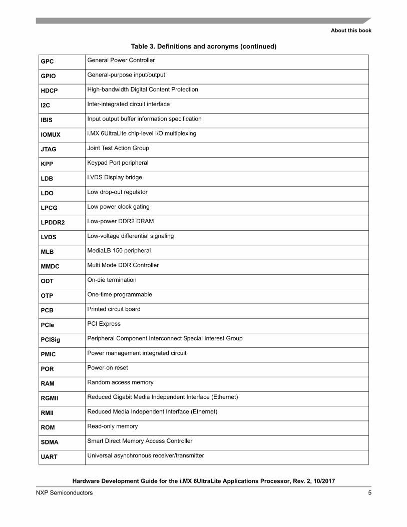
Table 3. Definitions and acronyms
Term Definition
ARM® Advanced RISC machines processor architecture
BGA Ball grid array package
BOM Bill of materials
BSDL Boundary scan description language
CAN Flexible Controller Area Network peripheral
CCM Clock Controller Module
DDR Dual data rate DRAM
DDR3 DDR3 DRAM
DDR3L Low voltage DDR3 DRAM
DDR3U Ultra low voltage DDR3 DRAM
DRAM Dynamic random access memory
ECSPI Enhanced Configurable SPI peripheral
EIM External Interface Module
ENET 10/100/1000-Mbps Ethernet MAC peripheral
EPIT Enhanced Periodic Interrupt Timer peripheral
ESR Equivalent series resistance (of a crystal)
NXP NXP Semiconductors
GND Ground
Hardware Development Guide for the i.MX 6UltraLite Applications Processor, Rev. 2, 10/2017
NXP Semiconductors 5
About this book
GPC General Power Controller
GPIO General-purpose input/output
HDCP High-bandwidth Digital Content Protection
I2C Inter-integrated circuit interface
IBIS Input output buffer information specification
IOMUX i.MX 6UltraLite chip-level I/O multiplexing
JTAG Joint Test Action Group
KPP Keypad Port peripheral
LDB LVDS Display bridge
LDO Low drop-out regulator
LPCG Low power clock gating
LPDDR2 Low-power DDR2 DRAM
LVDS Low-voltage differential signaling
MLB MediaLB 150 peripheral
MMDC Multi Mode DDR Controller
ODT On-die termination
OTP One-time programmable
PCB Printed circuit board
PCIe PCI Express
PCISig Peripheral Component Interconnect Special Interest Group
PMIC Power management integrated circuit
POR Power-on reset
RAM Random access memory
RGMII Reduced Gigabit Media Independent Interface (Ethernet)
RMII Reduced Media Independent Interface (Ethernet)
ROM Read-only memory
SDMA Smart Direct Memory Access Controller
UART Universal asynchronous receiver/transmitter
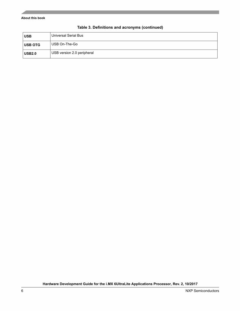
Table 3. Definitions and acronyms (continued)
Hardware Development Guide for the i.MX 6UltraLite Applications Processor, Rev. 2, 10/2017
6 NXP Semiconductors
About this book
USB Universal Serial Bus
USB OTG USB On-The-Go
USB2.0 USB version 2.0 peripheral
Table 3. Definitions and acronyms (continued)
Hardware Development Guide for the i.MX 6UltraLite Applications Processor, Rev. 2, 10/2017
NXP Semiconductors 7
i.MX 6UltraLite design checklist
2 i.MX 6UltraLite design checklist This document provides a design checklist for the i.MX 6UltraLite processor.
The design checklist tables contain recommendations for optimal design. Where appropriate, the checklist tables also provide an explanation of the recommendation so that users have a greater understanding of why certain techniques are recommended. All supplemental tables referenced by the checklist appear in sections following the design checklist tables.
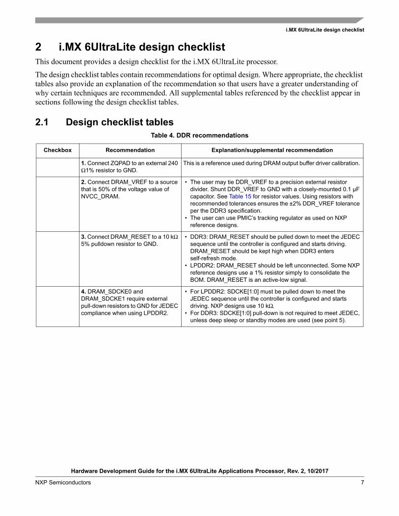
2.1 Design checklist tables Table 4. DDR recommendations
Checkbox Recommendation Explanation/supplemental recommendation
1. Connect ZQPAD to an external 240 Ω1% resistor to GND.
This is a reference used during DRAM output buffer driver calibration.
2. Connect DRAM_VREF to a source that is 50% of the voltage value of NVCC_DRAM.
• The user may tie DDR_VREF to a precision external resistor divider. Shunt DDR_VREF to GND with a closely-mounted 0.1 μF capacitor. See Table 15 for resistor values. Using resistors with recommended tolerances ensures the ±2% DDR_VREF tolerance per the DDR3 specification.
• The user can use PMIC’s tracking regulator as used on NXP reference designs.
3. Connect DRAM_RESET to a 10 kΩ 5% pulldown resistor to GND.
• DDR3: DRAM_RESET should be pulled down to meet the JEDEC sequence until the controller is configured and starts driving. DRAM_RESET should be kept high when DDR3 enters self-refresh mode.
• LPDDR2: DRAM_RESET should be left unconnected. Some NXP reference designs use a 1% resistor simply to consolidate the BOM. DRAM_RESET is an active-low signal.
4. DRAM_SDCKE0 and DRAM_SDCKE1 require external pull-down resistors to GND for JEDEC compliance when using LPDDR2.
• For LPDDR2: SDCKE[1:0] must be pulled down to meet the JEDEC sequence until the controller is configured and starts driving. NXP designs use 10 kΩ.
• For DDR3: SDCKE[1:0] pull-down is not required to meet JEDEC, unless deep sleep or standby modes are used (see point 5).
Hardware Development Guide for the i.MX 6UltraLite Applications Processor, Rev. 2, 10/2017
8 NXP Semiconductors
i.MX 6UltraLite design checklist
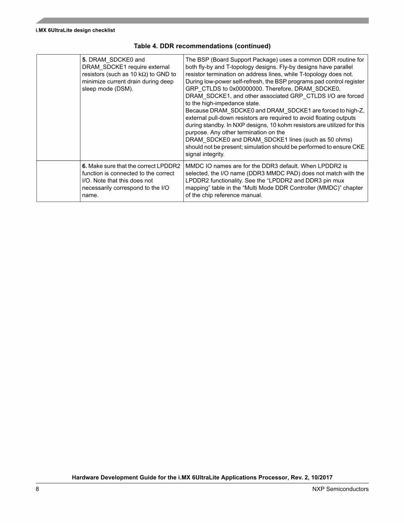
5. DRAM_SDCKE0 and DRAM_SDCKE1 require external resistors (such as 10 kΩ) to GND to minimize current drain during deep sleep mode (DSM).
The BSP (Board Support Package) uses a common DDR routine for both fly-by and T-topology designs. Fly-by designs have parallel resistor termination on address lines, while T-topology does not. During low-power self-refresh, the BSP programs pad control register GRP_CTLDS to 0x00000000. Therefore, DRAM_SDCKE0, DRAM_SDCKE1, and other associated GRP_CTLDS I/O are forced to the high-impedance state. Because DRAM_SDCKE0 and DRAM_SDCKE1 are forced to high-Z, external pull-down resistors are required to avoid floating outputs during standby. In NXP designs, 10 kohm resistors are utilized for this purpose. Any other termination on the DRAM_SDCKE0 and DRAM_SDCKE1 lines (such as 50 ohms) should not be present; simulation should be performed to ensure CKE signal integrity.
6. Make sure that the correct LPDDR2 function is connected to the correct I/O. Note that this does not necessarily correspond to the I/O name.
MMDC IO names are for the DDR3 default. When LPDDR2 is selected, the I/O name (DDR3 MMDC PAD) does not match with the LPDDR2 functionality. See the “LPDDR2 and DDR3 pin mux mapping” table in the “Multi Mode DDR Controller (MMDC)” chapter of the chip reference manual.
Table 4. DDR recommendations (continued)
Hardware Development Guide for the i.MX 6UltraLite Applications Processor, Rev. 2, 10/2017
NXP Semiconductors 9
i.MX 6UltraLite design checklist
Table 5. LCD recommendations for developer’s boot modes
Checkbox Recommendation Explanation/supplemental recommendation
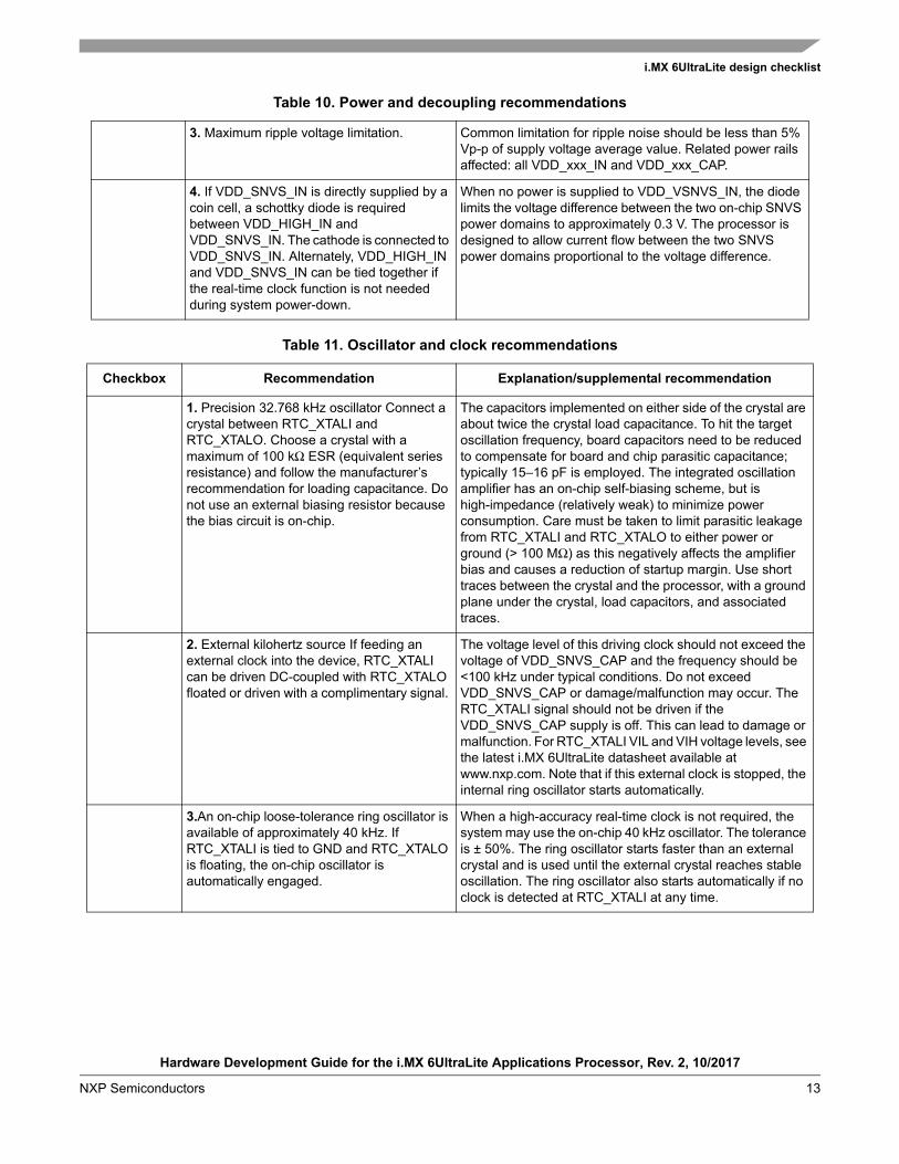
1. When LCD boot signals are used as the system’s LCD signals, other functions, or GPIO outputs after boot, use a passive resistor network to select the desired boot mode for development boards.
Because only resistors are used, LCD bus loads can cause current drain, leading to higher (false) supply current measurements. Each LCD boot signal should connect to a series resistor to isolate the bus from the resistors and/or switchers; see Figure 1. Each configured LCD boot signal sees either a 10 kΩ pulldown or a 10 kΩ pullup. For each switch-enabled pulled-up signal, the supply is presented with a 10 kΩ current load. An alternate approach using buffers is implemented in the i.MX 6UltraLite EVK development board design. Either of these implementations is acceptable.
2. To reduce incorrect boot-up mode selections, do one of the following: • Use LCD boot interface lines only as
processor outputs. Ensure LCD boot interface lines are not loaded down such that the level is interpreted as low during power-up, when the intent is to be a high level, or vice versa.
• If an LCD boot signal must be configured as an input, isolate the LCD signal from the target driving source with one analog switch and apply the logic value with a second analog switch. Alternately, peripheral devices with three-state outputs may be used; ensure the output is high-impedance during the boot up interval.
Using LCD boot interface lines as inputs may result in a wrong boot up due to the source overcoming the pull resistor value. A peripheral device may require the LCD signal to have an external or on-chip resistor to minimize signal floating. If the usage of the LCD boot signal affects the peripheral device, then an analog switch, open collector buffer, or equivalent should isolate the path. A pull-up or pull-down resistor at the peripheral device may be required to maintain the desired logic level. Review the switch or device data sheet for operating specifications.
3. The BOOT_CFG signals are required for proper functionality and operation and should not be left floating
See the “System Boot” chapter in your chip reference manual for the correct boot configuration. Note that an incorrect setting may result from an improper booting sequence.
Hardware Development Guide for the i.MX 6UltraLite Applications Processor, Rev. 2, 10/2017
10 NXP Semiconductors
i.MX 6UltraLite design checklist
Table 6. Boot mode and device recommendations
Checkbox Recommendation Explanation/supplemental recommendation
For BOOT_MODE1 and BOOT_MODE0, use one of the following options to achieve logic 0: • Tie to GND through any value
external resistor • Tie directly to GNDFor logic 1, use one of the following: • Tie directly to the VDD_SNVS_IN rail • Tie to the VDD_SNVS_IN rail
through an external resistor 10 kΩ. A value of 4.7 kΩ is preferred in high-noise environments.
If switch control is desired, no external pull down resistors are necessary. Simply connect SPST switches directly to the VDD_SNVS_IN rail. If desired, a 4.7 kΩ to 10 kΩ series resistor can be used when current drain is critical.
BOOT_MODE1 and BOOT_MODE0 each have on-chip pull-down devices with a nominal value of 100 kΩ, a projected minimum of 60 kΩ, and a projected maximum of 140 kΩ. Be aware that when these are logic high, current is drawn from the VDD_SNVS_IN supply. In production, when on-chip fuses determine the boot configuration, both boot mode inputs can be disconnected.
See the “Boot device interface allocation” section in the data sheet for detailed boot device connection design.
—
Table 7. I2C recommendations
Checkbox Recommendation Explanation/supplemental recommendation
1. Verify the target I2C interface clock rates.
The bus can only operate as fast as the slowest peripheral on the bus. If faster operation is required, move the slow devices to another I2C port.
2. Verify that the target I2C address range is supported and does no conflict with other peripherals. If there is an unavoidable address conflict, move the offending device to another I2C port.
These chips support up to four I2C ports. If it is undesirable to move a conflicting device to another I2C port, review the peripheral operation to see if it supports remapping the address.
3. Do not place more than one set of pull up resistors on the I2C lines.
This can result in excessive loading. Good design practice is to place one pair of pullups only.
Table 8. JTAG recommendations
Checkbox Recommendation Explanation/supplemental recommendation
1. Do not add external pull-up or pull-down resistors on JTAG_TDO.
JTAG_TDO is configured with an on-chip keeper circuit such that the floating condition is actively eliminated if an external pull resistor is not present. An external pull resistor on JTAG_TDO is detrimental. See Table 2-15 for a summary of the JTAG interface.
Hardware Development Guide for the i.MX 6UltraLite Applications Processor, Rev. 2, 10/2017
NXP Semiconductors 11
i.MX 6UltraLite design checklist
2. Ensure that the on-chip pull up/pull down configuration is followed if external resistors are used with JTAG signals (with the exception of JTAG_TDO). For example, do not use an external pull-down on an input that has an on-chip pull-up.
External resistors can be used with all JTAG signals except JTAG_TDO, but they are not required. See Table 16 for a summary of the JTAG interface.
3. JTAG_MOD may be referred to as SJC_MOD in some documents. Both names refer to the same signal. JTAG_MOD should be externally connected to GND for normal operation in a system. Termination to GND through an external pull down resistor is allowed. Use 4.7 kΩ.
When JTAG_MOD is low, the JTAG interface is configured for common software debug, adding all the system TAPs to the chain. When JTAG_MOD is high, the JTAG interface is configured to a mode compliant with the IEEE 1149.1 standard.
Table 9. Power supply decoupling recommendations
Checkbox Supply Decoupling and bulk caps (min qty) Notes
VDD_SOC_IN 2×0.22uF²+1×4.7uF¹+1×22uF³ 14x14 package: Place 22 uF cap and one of the 0.22uF caps next to the ball K10.
VDD_ARM_CAP 2×0.22uF²+1×22uF³ 14x14 package: Place 22 uF cap and oneof the 0.22uF caps next to the ball G9.Place "+" within 50 mils of via. Do notconnect any loads to VDDARM_CAP.
VDD_SOC_CAP 3×0.22uF²+1×22uF³ 14x14 package: Place 22 uF cap and oneof the 0.22uF caps next to the ball AA10.Place "+" within 50 mils of via.
VDD_HIGH_IN 1×0.22uF²+1×4.7uF¹ —
VDD_HIGH_CAP 1×0.22uF²+1×10uF¹ VDDHIGH_CAP is restricted to MX6ULloads.
VDD_SNVS_IN 1×0.22uF² —
VDD_SNVS_CAP 1×0.22uF² If the nominal value is larger thanrecommended, power-up/down ramptime is excessive and suspend/resumeoperation cannot be guaranteed. Select asmall capacitor with low ESR. Do notconnect any loads to VDD_SNVS_CAP.
NVCC_DRAM 4×0.22uF²+1×22uF³ Can be separated into four 4.7uF capsinstead of single 22 uF
NVCC_PLL 1×0.22uF²+1×10uF¹ Do not connect any loads to this LDOoutput.
Table 8. JTAG recommendations (continued)
Hardware Development Guide for the i.MX 6UltraLite Applications Processor, Rev. 2, 10/2017
12 NXP Semiconductors
i.MX 6UltraLite design checklist
1 Use the smallest capacitor package size allowed with your design rules2 For 0.22 μF capacitors, use 0402 package 3 For 22 μF capacitors, 0603 package preferred; 0805 and 1206 are acceptable
NVCC_xxxx 1×0.22uF² One capacitor per via. Grouped NVCCballs can share a capacitor.
VDD_USB_CAP 1×0.1uF+1×10uF¹ May use a single 10 uF capacitor insteadof 2 ×4.7 uF capacitors. Do not connectany loads to this LDO output.
USB_OTG1_VBUS 1×1uF¹ 10V rated
USB_OTG2_VBUS 1×1uF¹ 10V rated
Table 10. Power and decoupling recommendations
Checkbox Recommendation Explanation/supplemental recommendation
1. Comply with the power-up sequence guidelines as described in the data sheet to guarantee reliable operation of the device.
Any deviation from these sequences may result in the following situations: • Excessive current during power-up phase • Prevention of the device from booting • Irreversible damage to the processor (worst-case
scenario)
2. Do not overload coin cell backup power rail VDD_SNVS_IN. Note that the following I/Os are associated with VDD_SNVS_IN; most inputs have on-chip pull resistors and do not require external resistors: • POR_B – configurable on-chip pullup • ONOFF – on-chip pullup • BOOT_MODE0 – on-chip pulldown • BOOT_MODE1 – on-chip pulldown • TAMPER – on-chip keeper • PMIC_STBY_REQ – configurable output • PMIC_ON_REQ – push-pull output • TEST_MODE – on-chip pulldown
Concerning i.MX 6UltraLite: • When VDD_SNVS_IN = VDD_HIGH_IN, SNVS domain
current is drawn from both equally. • When VDD_HIGH_IN > VDD_SNVS_IN, VDD_HIGH_IN
supplies all SNVS domain current and current flows into VDD_SNVS_IN to charge a coin cell battery.
• When VDD_SNVS_IN > VDD_HIGH_IN, VDD_SNVS_IN supplies current to SNVS, and some current flows into VDD_HIGH_IN.
Note: VDD_HIGH_IN must be valid (above the internal detector threshold, 2.4 V typ) for the current flow to occur. Thus, current flow only happens when VDD_HIGH_IN is powered to a level below VDD_SNVS_IN. If VDD_HIGH_IN is off or low, no extra current is drawn from VDD_SNVS_IN. The whole circuit assumes it is charging a coin cell and starts charging when VDD_HIGH_IN is valid. If you are driving VDD_SNVS_IN with a non-battery power source, it must be at the same level as VDD_HIGH_IN or current will flow between them. • When VDD_SNVS_IN is not powered by a battery, it is
recommended that VDD_SNVS_IN = VDD_HIGH_IN. If VDD_SNVS_IN is tied to a battery, the battery eventually discharges to a value equal to that of VDD_HIGH_IN and never subsequently charges above VDD_HIGH_IN. The battery chemistry may add restrictions to VDD_HIGH_IN’s voltage range. External charging components should be based on the battery manufacturer's specifications.
Table 9. Power supply decoupling recommendations
Hardware Development Guide for the i.MX 6UltraLite Applications Processor, Rev. 2, 10/2017
NXP Semiconductors 13
i.MX 6UltraLite design checklist
3. Maximum ripple voltage limitation. Common limitation for ripple noise should be less than 5% Vp-p of supply voltage average value. Related power rails affected: all VDD_xxx_IN and VDD_xxx_CAP.
4. If VDD_SNVS_IN is directly supplied by a coin cell, a schottky diode is required between VDD_HIGH_IN and VDD_SNVS_IN. The cathode is connected to VDD_SNVS_IN. Alternately, VDD_HIGH_IN and VDD_SNVS_IN can be tied together if the real-time clock function is not needed during system power-down.
When no power is supplied to VDD_VSNVS_IN, the diode limits the voltage difference between the two on-chip SNVS power domains to approximately 0.3 V. The processor is designed to allow current flow between the two SNVS power domains proportional to the voltage difference.
Table 11. Oscillator and clock recommendations
Checkbox Recommendation Explanation/supplemental recommendation
1. Precision 32.768 kHz oscillator Connect a crystal between RTC_XTALI and RTC_XTALO. Choose a crystal with a maximum of 100 kΩ ESR (equivalent series resistance) and follow the manufacturer’s recommendation for loading capacitance. Do not use an external biasing resistor because the bias circuit is on-chip.
The capacitors implemented on either side of the crystal are about twice the crystal load capacitance. To hit the target oscillation frequency, board capacitors need to be reduced to compensate for board and chip parasitic capacitance; typically 15–16 pF is employed. The integrated oscillation amplifier has an on-chip self-biasing scheme, but is high-impedance (relatively weak) to minimize power consumption. Care must be taken to limit parasitic leakage from RTC_XTALI and RTC_XTALO to either power or ground (> 100 MΩ) as this negatively affects the amplifier bias and causes a reduction of startup margin. Use short traces between the crystal and the processor, with a ground plane under the crystal, load capacitors, and associated traces.
2. External kilohertz source If feeding an external clock into the device, RTC_XTALI can be driven DC-coupled with RTC_XTALO floated or driven with a complimentary signal.
The voltage level of this driving clock should not exceed the voltage of VDD_SNVS_CAP and the frequency should be <100 kHz under typical conditions. Do not exceed VDD_SNVS_CAP or damage/malfunction may occur. The RTC_XTALI signal should not be driven if the VDD_SNVS_CAP supply is off. This can lead to damage or malfunction. For RTC_XTALI VIL and VIH voltage levels, see the latest i.MX 6UltraLite datasheet available at www.nxp.com. Note that if this external clock is stopped, the internal ring oscillator starts automatically.
3.An on-chip loose-tolerance ring oscillator is available of approximately 40 kHz. If RTC_XTALI is tied to GND and RTC_XTALO is floating, the on-chip oscillator is automatically engaged.
When a high-accuracy real-time clock is not required, the system may use the on-chip 40 kHz oscillator. The tolerance is ± 50%. The ring oscillator starts faster than an external crystal and is used until the external crystal reaches stable oscillation. The ring oscillator also starts automatically if no clock is detected at RTC_XTALI at any time.
Table 10. Power and decoupling recommendations
Hardware Development Guide for the i.MX 6UltraLite Applications Processor, Rev. 2, 10/2017
14 NXP Semiconductors
i.MX 6UltraLite design checklist
4. Precision 24 MHz oscillator Connect a fundamental-mode crystal between XTALI and XTALO. An 80 typical ESR crystal rated for a maximum drive level of 250 W is acceptable.Alternately, a 50 typical ESR crystal rated for a maximum drive level of 200 W may be used. See the engineering bulletin EB830 on www.nxp.com for additional options.
NXP BSP software requires 24 MHz on this clock. This clock is used as a reference for USB and PCIe, so there are strict frequency tolerance and jitter requirements. See Table 17 for guidelines. See the crystal oscillator (XTALOSC) reference manual chapter and relevant interface specification chapters for details. To access a calculator for the 24 MHz crystal drive level, see EB830 on the i.MX Community.
5. External megahertz source If feeding an external clock into the device: • A single ended external clock source can
be used to drive XTALI for MX6UL TO1.1. In this configuration, XTALO should be left externally floating.
• A differential external clock source can be used to drive both XTALI and XTALO for MX6UL TO1.1.
For XTALI VIL and VIH voltage levels, see the latest i.MX 6 UltraLite datasheet. See the crystal oscillator (XTALOSC) reference manual chapter and relevant interface specification chapters for details.
6. CCM_CLK1_P/ CCM_CLK1_N are LVDS input/output differential pairs compatible with TIA/EIA-644 standard. The frequency range is 0 to 600 MHz. Alternatively, a single-ended signal can be used to drive a CCM_CLKx_P input. In this case, the corresponding CCM_CLKx_N input should be tied to a constant voltage level equal to 50% of VDD_HIGH_CAP. Termination should be provided with high-frequency signals. See the LVDS pad electrical specification in the data sheet for further details. After initialization, the CCM_CLKx inputs/outputs can be disabled (if not used) by the PMU_MISC1 register. If unused, any or both of the CCM_CLKx_N/P pairs may be left floating.
The clock inputs/outputs are general-purpose differential high-speed clock Input/outputs. Any or both of them can be configured: • As inputs to feed external reference clocks to the on-chip
PLLs and/or modules. • As outputs to be used as either a reference clock or as a
functional clock for peripherals.
7. Bias XTALI with a 2.2 M resistor to GND. Mount the resistor close to the XTALI ball
The XTALI bias must be adjusted externally to ensure reasonable start-up time.
Table 11. Oscillator and clock recommendations (continued)
Hardware Development Guide for the i.MX 6UltraLite Applications Processor, Rev. 2, 10/2017
NXP Semiconductors 15
i.MX 6UltraLite design checklist
The following figure provides supporting information for Table 18.
Table 12. Reset and ON OFF recommendations
Checkbox Recommendation Explanation/supplemental recommendation
1. If the external POR_B signal is used to control the processor POR, then POR_B must be immediately asserted at power-up and remain asserted until the VDD_ARM_CAP and VDD_SOC_CAP supplies are stable. VDD_SOC_IN may be applied in either order with no restrictions. In the absence of an external reset feeding the SRC_POR_B input, the internal POR module takes control.
A reset switch may be wired to the chip’s POR_B, which is a cold-reset negative-logic input that resets all modules and logic in the IC. POR_B may be used in addition to internally generated power-on reset signal (logical AND, both internal and external signals are considered active low).
2. For portable applications, the ON/OFF input may be connected to an ON/OFF SPST push-button switch. On-chip debouncing is provided, and this input has an on-chip pull up. If not used, ON/OFF can be a no connect.
A brief connection to GND in OFF mode causes the internal power management state machine to change state to ON.In ON mode, a brief connection to GND generates an interrupt (intended to be a software-controllable power-down).An approximate 5 seconds or more to GND causes a forced OFF.
Table 13. USB recommendations
Checkbox Recommendation Explanation/supplemental recommendation
1. USB OTGTo comply with the USB OTG specification, the VBUS supply on the OTG connector should be off by default when the boards power up, and keeps off until OTG_ID is pulled low.
The processor can turn VBUS on when it’s required.
Table 14. Miscellaneous recommendations
Checkbox Recommendation Explanation/supplemental recommendation
1. The TEST_MODE input is internally connected to an on-chip pull down device. The user can either float this signal or tie it to GND.
This input is reserved for NXP manufacturing use.
2. GPANAIO must be a no connect. This output is reserved for NXP manufacturing use.
3. NC contacts are no connect and should be floated.
Depending on the feature set, some versions of the IC may have NC contacts connected inside the BGA.
Hardware Development Guide for the i.MX 6UltraLite Applications Processor, Rev. 2, 10/2017
16 NXP Semiconductors
i.MX 6UltraLite design checklist
Figure 1. Boot configuration for development mode
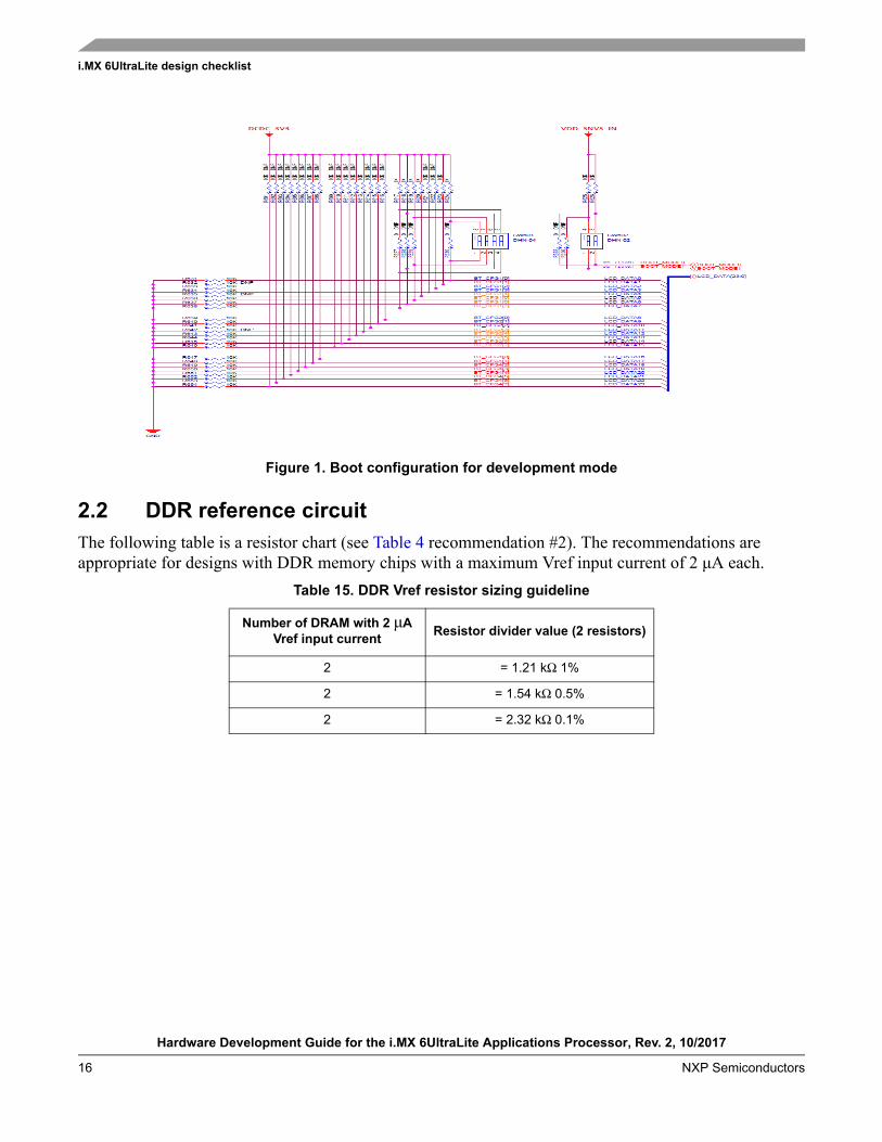
2.2 DDR reference circuit
The following table is a resistor chart (see Table 4 recommendation #2). The recommendations are appropriate for designs with DDR memory chips with a maximum Vref input current of 2 μA each.
Table 15. DDR Vref resistor sizing guideline
Number of DRAM with 2 μA Vref input current
Resistor divider value (2 resistors)
2 = 1.21 kΩ 1%
2 = 1.54 kΩ 0.5%
2 = 2.32 kΩ 0.1%
Hardware Development Guide for the i.MX 6UltraLite Applications Processor, Rev. 2, 10/2017
NXP Semiconductors 17
i.MX 6UltraLite design checklist
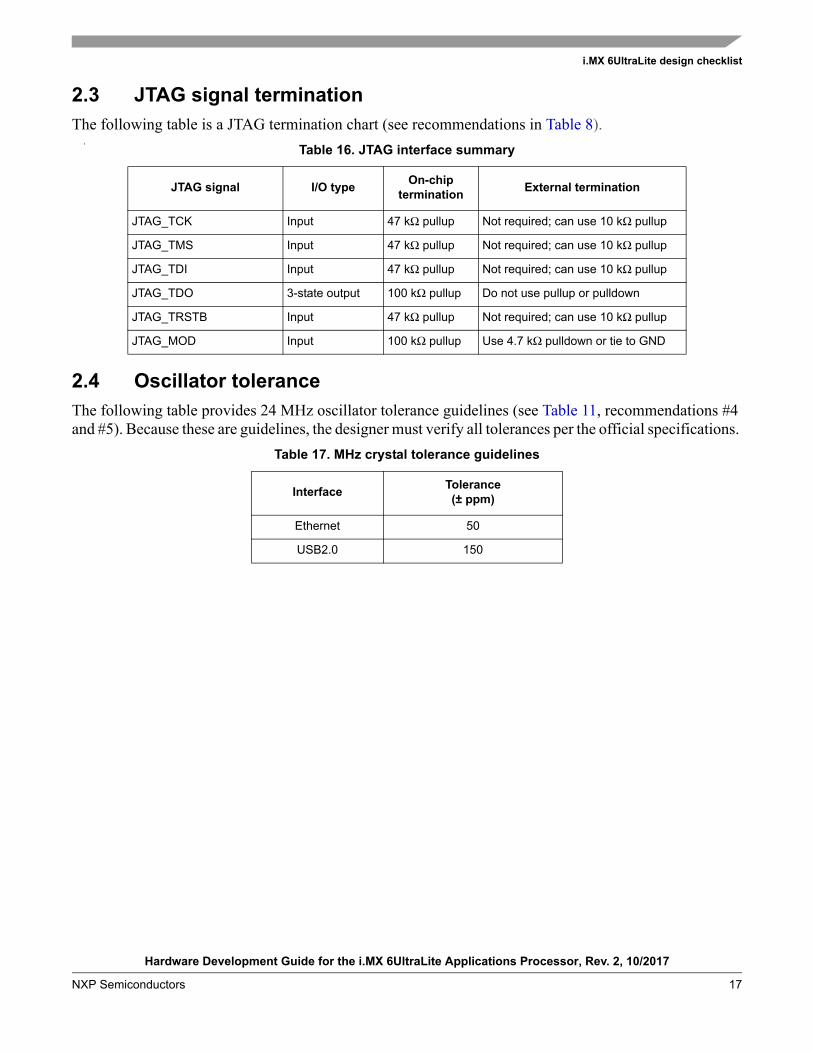
2.3 JTAG signal termination
The following table is a JTAG termination chart (see recommendations in Table 8). k
2.4 Oscillator tolerance
The following table provides 24 MHz oscillator tolerance guidelines (see Table 11, recommendations #4 and #5). Because these are guidelines, the designer must verify all tolerances per the official specifications.
Table 16. JTAG interface summary
JTAG signal I/O type On-chip
termination External termination
JTAG_TCK Input 47 kΩ pullup Not required; can use 10 kΩ pullup
JTAG_TMS Input 47 kΩ pullup Not required; can use 10 kΩ pullup
JTAG_TDI Input 47 kΩ pullup Not required; can use 10 kΩ pullup
JTAG_TDO 3-state output 100 kΩ pullup Do not use pullup or pulldown
JTAG_TRSTB Input 47 kΩ pullup Not required; can use 10 kΩ pullup
JTAG_MOD Input 100 kΩ pullup Use 4.7 kΩ pulldown or tie to GND
Table 17. MHz crystal tolerance guidelines
Interface Tolerance (± ppm)
Ethernet 50
USB2.0 150
Hardware Development Guide for the i.MX 6UltraLite Applications Processor, Rev. 2, 10/2017
18 NXP Semiconductors
i.MX 6UltraLite design checklist
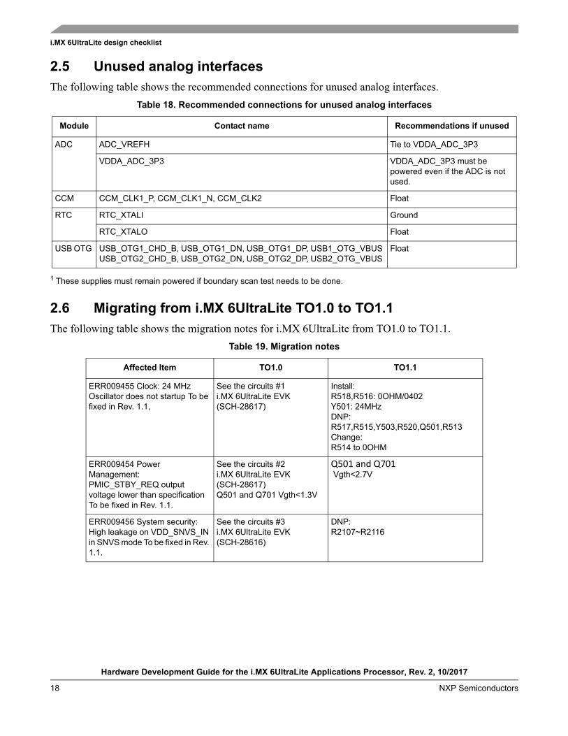
2.5 Unused analog interfaces
The following table shows the recommended connections for unused analog interfaces.
1 These supplies must remain powered if boundary scan test needs to be done.
2.6 Migrating from i.MX 6UltraLite TO1.0 to TO1.1
The following table shows the migration notes for i.MX 6UltraLite from TO1.0 to TO1.1.
Table 18. Recommended connections for unused analog interfaces
Module Contact name Recommendations if unused
ADC ADC_VREFH Tie to VDDA_ADC_3P3
VDDA_ADC_3P3 VDDA_ADC_3P3 must be powered even if the ADC is not used.
CCM CCM_CLK1_P, CCM_CLK1_N, CCM_CLK2 Float
RTC RTC_XTALI Ground
RTC_XTALO Float
USB OTG USB_OTG1_CHD_B, USB_OTG1_DN, USB_OTG1_DP, USB1_OTG_VBUS USB_OTG2_CHD_B, USB_OTG2_DN, USB_OTG2_DP, USB2_OTG_VBUS
Float
Table 19. Migration notes
Affected Item TO1.0 TO1.1
ERR009455 Clock: 24 MHz Oscillator does not startup To be fixed in Rev. 1.1,
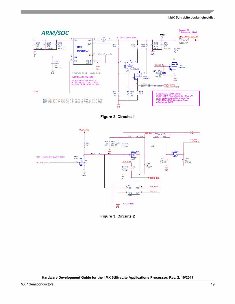
See the circuits #1i.MX 6UltraLite EVK (SCH-28617)
Install: R518,R516: 0OHM/0402 Y501: 24MHz DNP: R517,R515,Y503,R520,Q501,R513 Change: R514 to 0OHM
ERR009454 Power Management: PMIC_STBY_REQ output voltage lower than specification To be fixed in Rev. 1.1.
See the circuits #2i.MX 6UltraLite EVK (SCH-28617)Q501 and Q701 Vgth<1.3V
Q501 and Q701 Vgth<2.7V
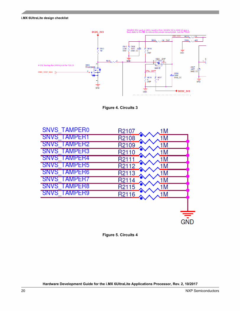
ERR009456 System security: High leakage on VDD_SNVS_IN in SNVS mode To be fixed in Rev. 1.1.
See the circuits #3i.MX 6UltraLite EVK (SCH-28616)
DNP: R2107~R2116
Hardware Development Guide for the i.MX 6UltraLite Applications Processor, Rev. 2, 10/2017
NXP Semiconductors 19
i.MX 6UltraLite design checklist
Figure 2. Circuits 1
Figure 3. Circuits 2
Hardware Development Guide for the i.MX 6UltraLite Applications Processor, Rev. 2, 10/2017
20 NXP Semiconductors
i.MX 6UltraLite design checklist
Figure 4. Circuits 3
Figure 5. Circuits 4
Hardware Development Guide for the i.MX 6UltraLite Applications Processor, Rev. 2, 10/2017
NXP Semiconductors 21
i.MX 6UltraLite layout recommendations
3 i.MX 6UltraLite layout recommendations
3.1 Introduction
This chapter provides recommendations to assist design engineers with the layout of an i.MX 6UltraLilte -based system.
3.2 Basic design recommendations
The i.MX 6UltraLite processor comes in multiple packages.
When using the Allegro tool, optimal practice is to use the footprint as created by NXP. When not using the Allegro tool, use the Allegro footprint export feature (supported by many tools). If export is not possible, create the footprint per the package mechanical dimensions outlined in the product data sheet.
Native Allegro layout and gerber files are available on www.nxp.com.
3.2.1 Placement of bulk and decoupling capacitors
Place small decoupling and larger bulk capacitors on the bottom side of the CPU.
The 0402 decoupling and 0603 bulk capacitors should be placed as close as possible to the power balls. The distance should be less than 50 mils. Additional bulk capacitors can be placed near the edge of the BGA via array. Placing the decoupling capacitors close to the power balls is critical to minimize inductance and ensure high-speed transient current demand by the processor.
A correct via size is critical for preserving adequate routing space. The recommended geometry for the via pads is: pad size 18 mils and drill 8 mils.
A preferred BGA power decoupling design layout is available through www.nxp.com. Customers should use the NXP design strategy for power and decoupling.
3.3 Stackup recommendations
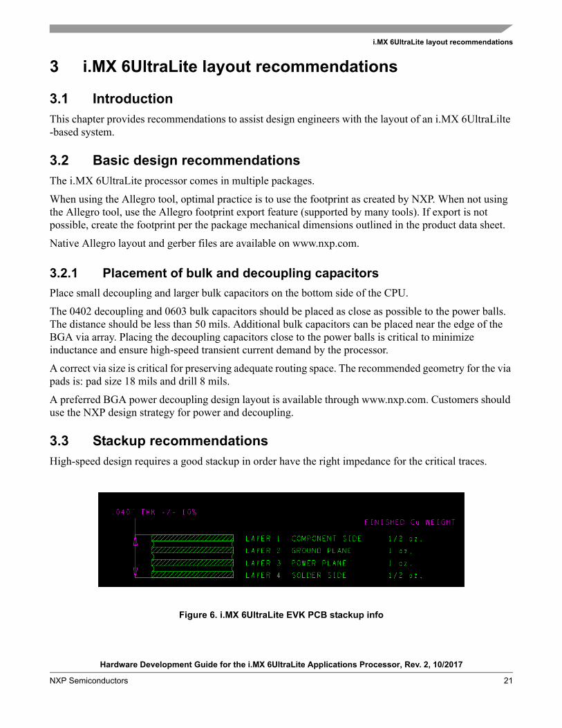
High-speed design requires a good stackup in order have the right impedance for the critical traces.
Figure 6. i.MX 6UltraLite EVK PCB stackup info
Hardware Development Guide for the i.MX 6UltraLite Applications Processor, Rev. 2, 10/2017
22 NXP Semiconductors
i.MX 6UltraLite layout recommendations
The constraints for the trace width may depend on a number of factors, such as the board stackup and associated dielectric and copper thickness, required impedance, and required current (for power traces). The NXP reference design uses a minimum trace width of 3 mils for the DDR routing. The stackup also determines the constraints for routing and spacing.
Consider the following when designing the stackup and selecting the material for your board.
• Board stack-up is critical for high-speed signal quality.
• You must preplan impedance of critical traces
• High-speed signals must have reference planes on adjacent layers to minimize cross-talk.
• NXP reference design equals Isola FR4.
• NXP validation boards equals Isola FR4.
• The recommended stackup is 4-layers, with the layer stack as shown in the following figure. The left hand image shows the detail provided by NXP inside the fabrication detail as a part of the Gerber files. The right hand side shows the solution suggested by the PCB fabrication company for our requirements.
The following table shows the i.MX 6UltraLite EVK PCB stackup implementation:
3.4 DDR connection information
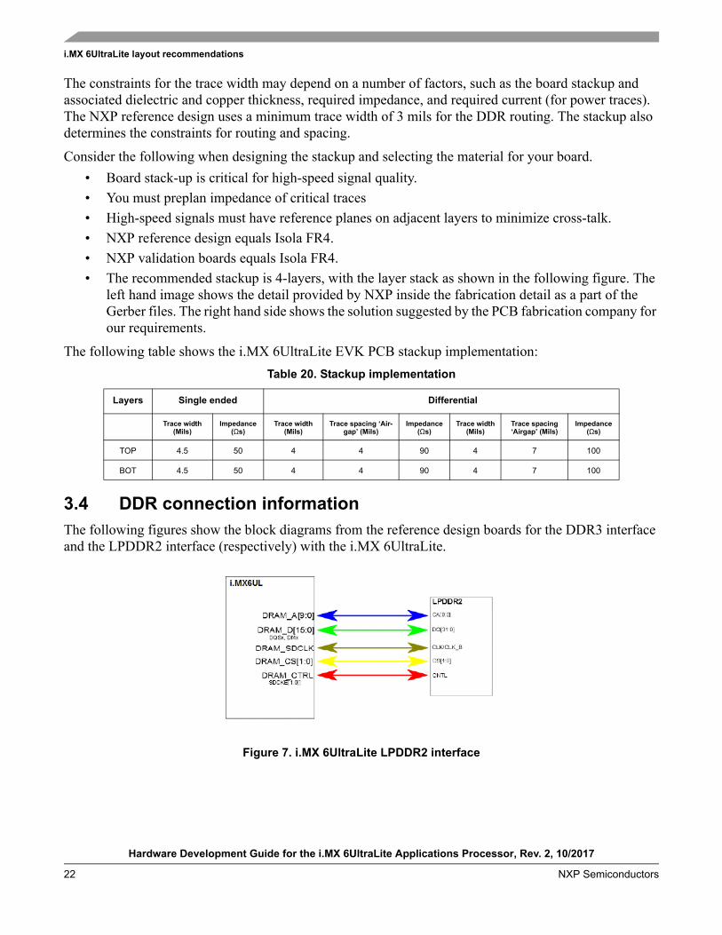
The following figures show the block diagrams from the reference design boards for the DDR3 interface and the LPDDR2 interface (respectively) with the i.MX 6UltraLite.
Figure 7. i.MX 6UltraLite LPDDR2 interface
Table 20. Stackup implementation
Layers Single ended Differential
Trace width (Mils)
Impedance (Ωs)
Trace width (Mils)
Trace spacing ‘Air-gap’ (Mils)
Impedance (Ωs)
Trace width (Mils)
Trace spacing ‘Airgap’ (Mils)
Impedance (Ωs)
TOP 4.5 50 4 4 90 4 7 100
BOT 4.5 50 4 4 90 4 7 100
Hardware Development Guide for the i.MX 6UltraLite Applications Processor, Rev. 2, 10/2017
NXP Semiconductors 23
i.MX 6UltraLite layout recommendations
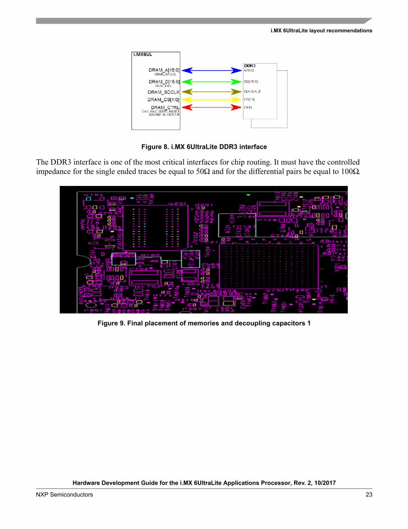
Figure 8. i.MX 6UltraLite DDR3 interface
The DDR3 interface is one of the most critical interfaces for chip routing. It must have the controlled impedance for the single ended traces be equal to 50Ω and for the differential pairs be equal to 100Ω.
Figure 9. Final placement of memories and decoupling capacitors 1
Hardware Development Guide for the i.MX 6UltraLite Applications Processor, Rev. 2, 10/2017
24 NXP Semiconductors
i.MX 6UltraLite layout recommendations
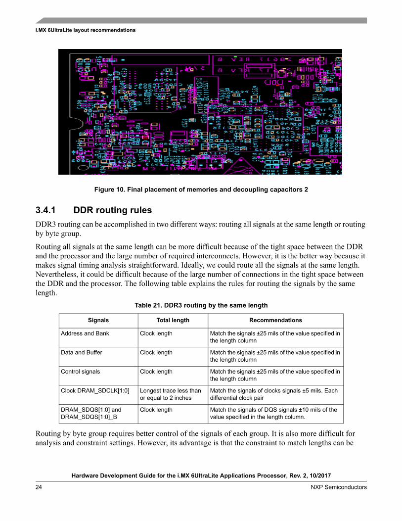
Figure 10. Final placement of memories and decoupling capacitors 2
3.4.1 DDR routing rules
DDR3 routing can be accomplished in two different ways: routing all signals at the same length or routing by byte group.
Routing all signals at the same length can be more difficult because of the tight space between the DDR and the processor and the large number of required interconnects. However, it is the better way because it makes signal timing analysis straightforward. Ideally, we could route all the signals at the same length. Nevertheless, it could be difficult because of the large number of connections in the tight space between the DDR and the processor. The following table explains the rules for routing the signals by the same length.
Routing by byte group requires better control of the signals of each group. It is also more difficult for analysis and constraint settings. However, its advantage is that the constraint to match lengths can be
Table 21. DDR3 routing by the same length
Signals Total length Recommendations
Address and Bank Clock length Match the signals ±25 mils of the value specified in the length column
Data and Buffer Clock length Match the signals ±25 mils of the value specified in the length column
Control signals Clock length Match the signals ±25 mils of the value specified in the length column
Clock DRAM_SDCLK[1:0] Longest trace less than or equal to 2 inches
Match the signals of clocks signals ±5 mils. Each differential clock pair
DRAM_SDQS[1:0] and DRAM_SDQS[1:0]_B
Clock length Match the signals of DQS signals ±10 mils of the value specified in the length column.
Hardware Development Guide for the i.MX 6UltraLite Applications Processor, Rev. 2, 10/2017
NXP Semiconductors 25
i.MX 6UltraLite layout recommendations
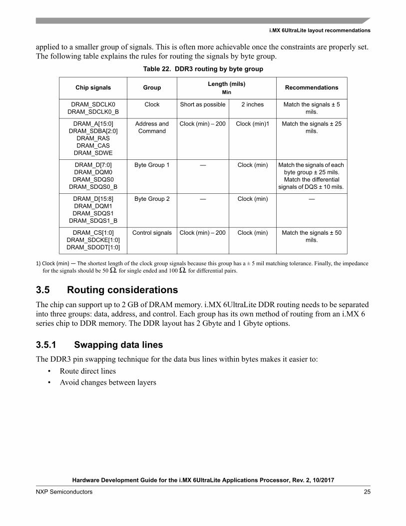
applied to a smaller group of signals. This is often more achievable once the constraints are properly set. The following table explains the rules for routing the signals by byte group.
1) Clock (min) — The shortest length of the clock group signals because this group has a ± 5 mil matching tolerance. Finally, the impedance for the signals should be 50 Ω. for single ended and 100 Ω. for differential pairs.
3.5 Routing considerations
The chip can support up to 2 GB of DRAM memory. i.MX 6UltraLite DDR routing needs to be separated into three groups: data, address, and control. Each group has its own method of routing from an i.MX 6 series chip to DDR memory. The DDR layout has 2 Gbyte and 1 Gbyte options.
3.5.1 Swapping data lines
The DDR3 pin swapping technique for the data bus lines within bytes makes it easier to:
• Route direct lines
• Avoid changes between layers
Table 22. DDR3 routing by byte group
Chip signals Group Length (mils)
Min Recommendations
DRAM_SDCLK0 DRAM_SDCLK0_B
Clock Short as possible 2 inches Match the signals ± 5 mils.
DRAM_A[15:0] DRAM_SDBA[2:0]
DRAM_RAS DRAM_CAS
DRAM_SDWE
Address and Command
Clock (min) – 200 Clock (min)1 Match the signals ± 25 mils.
DRAM_D[7:0] DRAM_DQM0 DRAM_SDQS0
DRAM_SDQS0_B
Byte Group 1 — Clock (min) Match the signals of each byte group ± 25 mils. Match the differential
signals of DQS ± 10 mils.
DRAM_D[15:8] DRAM_DQM1 DRAM_SDQS1
DRAM_SDQS1_B
Byte Group 2 — Clock (min) —
DRAM_CS[1:0] DRAM_SDCKE[1:0] DRAM_SDODT[1:0]
Control signals Clock (min) – 200 Clock (min) Match the signals ± 50 mils.
Hardware Development Guide for the i.MX 6UltraLite Applications Processor, Rev. 2, 10/2017
26 NXP Semiconductors
i.MX 6UltraLite layout recommendations
The rules are as follows:
• Hardware write leveling – lowest order bit within byte lane must remain on lowest order bit of lane by JEDEC compliance (see the “Write Leveling” section in JESD79-3E)
— The lowest bit of each byte must be aligned between the i.MX 6UltraLite and DDR chips. For example, D0 of i.MX 6UltraLite to D0 of DDR chip, D8 of i.MX 6UltraLite to D8 of DDR chip.
— Other data lines free to swap within byte lane
• JEDEC DDR3 memory restrictions are:
— No restrictions for complete byte lane swapping
— DQS and DQM must follow lanes
NOTE
If byte lane swapping was done, target DDR IC register read value must be transposed according to the data line swapping.
3.5.2 High speed signal routing recommendations
The following list provides recommendations for routing traces for high speed signals. Note that the propagation delay and the impedance control should match in order to have the correct communication with the devices.
• High-speed signals (DDR, RMII, display) must not cross gaps in the reference plane.
• Avoid creating slots, voids, and splits in reference planes. Review via voids to ensure they do not create splits (space out vias).
• Provide ground return vias within 100 mils distance from signal layer-transition vias when transitioning between different reference ground planes.
• A solid GND plane must be directly under crystal, associated components, and traces.
• Clocks or strobes that are on the same layer need at least 2.5× spacing from an adjacent trace (2.5× height from reference plane) to reduce cross-talk.
• Provide ground return vias within 100 mils distance from signal layer-transition vias when transitioning between different reference ground planes.
• All synchronous modules should have bus length matching and relative clock length control. For SD module interfaces:
— Match data and CMD trace lengths (length delta depends on bus rates)
— CLK should be longer than the longest signal in the Data/CMD group (+5 mils)
— Similar DDR rules must be followed for data, address and control as for SD module interfaces.
Hardware Development Guide for the i.MX 6UltraLite Applications Processor, Rev. 2, 10/2017
NXP Semiconductors 27
i.MX 6UltraLite layout recommendations
3.6 DDR power recommendations
The following recommendations apply to the VREF (P0V675_REFDDR) voltage reference plane.
• Use < 30 mils trace between decoupling cap and destination.
• Maintain a 25 mils clearance from other nets.
Decouple using distributed 0.22 uF capacitors by the regulator, controller, and devices.
• Place one 1.0 uF near the source of VREF: one near the VREF pin on the controller and two between the controller and the devices.
3.7 USB recommendations
Use the following recommendations for the USB.
• Route the high speed clocks and the DP and DM differential pair first.
• Route DP and DM signals on the top or bottom layer of the board.
• The trace width and spacing of the DP and DM signals should meet the differential impedance requirement of 90 Ω.
• Route traces over continuous planes (power and ground).
— They should not pass over any power/GND plane slots or anti-etch.
— When placing connectors, make sure the ground plane clearouts around each pin have ground continuity between all pins.
• Maintain the parallelism (skew matched) between DP and DM, and match overall differential length difference to less than 5 mils.
• Maintain symmetric routing for each differential pair.
Do not route DP and DM traces under oscillators or parallel to clock traces and/or data buses.
• Minimize the lengths of high speed signals that run parallel to the DP and DM pair.
• Keep DP and DM traces as short as possible.
• Route DP and DM signals with a minimum amount of corners. Use 45-degree turns instead of 90-degree turns.
• Avoid layer changes (vias) on DP and DM signals. Do not create stubs or branches.
• Provide ground return vias within 50 mils distance from signal layer-transition vias when transitioning between different reference ground planes.
Hardware Development Guide for the i.MX 6UltraLite Applications Processor, Rev. 2, 10/2017
28 NXP Semiconductors
i.MX 6UltraLite layout recommendations
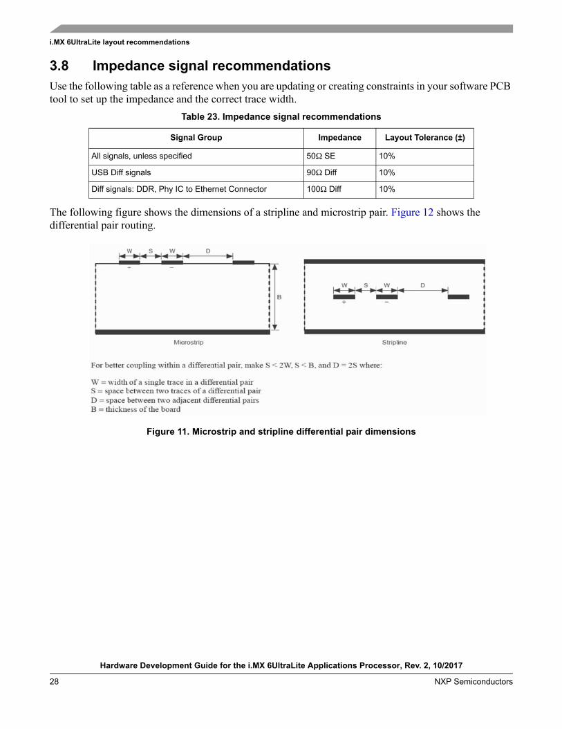
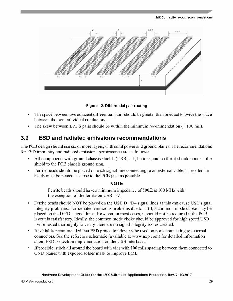
3.8 Impedance signal recommendations
Use the following table as a reference when you are updating or creating constraints in your software PCB tool to set up the impedance and the correct trace width.
The following figure shows the dimensions of a stripline and microstrip pair. Figure 12 shows the differential pair routing.
Figure 11. Microstrip and stripline differential pair dimensions
Table 23. Impedance signal recommendations
Signal Group Impedance Layout Tolerance (±)
All signals, unless specified 50Ω SE 10%
USB Diff signals 90Ω Diff 10%
Diff signals: DDR, Phy IC to Ethernet Connector 100Ω Diff 10%
Hardware Development Guide for the i.MX 6UltraLite Applications Processor, Rev. 2, 10/2017
NXP Semiconductors 29
i.MX 6UltraLite layout recommendations
Figure 12. Differential pair routing
• The space between two adjacent differential pairs should be greater than or equal to twice the space between the two individual conductors.
• The skew between LVDS pairs should be within the minimum recommendation (± 100 mil).
3.9 ESD and radiated emissions recommendations
The PCB design should use six or more layers, with solid power and ground planes. The recommendations for ESD immunity and radiated emissions performance are as follows:
• All components with ground chassis shields (USB jack, buttons, and so forth) should connect the shield to the PCB chassis ground ring.
• Ferrite beads should be placed on each signal line connecting to an external cable. These ferrite beads must be placed as close to the PCB jack as possible.
NOTE
Ferrite beads should have a minimum impedance of 500Ω at 100 MHz with the exception of the ferrite on USB_5V.
• Ferrite beads should NOT be placed on the USB D+/D– signal lines as this can cause USB signal integrity problems. For radiated emissions problems due to USB, a common mode choke may be placed on the D+/D– signal lines. However, in most cases, it should not be required if the PCB layout is satisfactory. Ideally, the common mode choke should be approved for high speed USB use or tested thoroughly to verify there are no signal integrity issues created.
• It is highly recommended that ESD protection devices be used on ports connecting to external connectors. See the reference schematic (available at www.nxp.com) for detailed information about ESD protection implementation on the USB interfaces.
• If possible, stitch all around the board with vias with 100 mils spacing between them connected to GND planes with exposed solder mask to improve EMI.
Hardware Development Guide for the i.MX 6UltraLite Applications Processor, Rev. 2, 10/2017
30 NXP Semiconductors
i.MX 6UltraLite layout recommendations
3.10 Component placement recommendations
Adhere to the following recommendations when placing components.
• Place components such that short and/or critical routes can be easily laid out.
— Critical routes determine component location.
— Orient devices to facilitate routes (minimize length and crossovers).
• Consider placing the following pairings adjacent.
— i.MX and DDR
— PHY and associated jack
— Jack and CODEC input
— Bluetooth® (or other RF) and antenna
3.11 Reducing skew and phase problems in deferential pairs traces
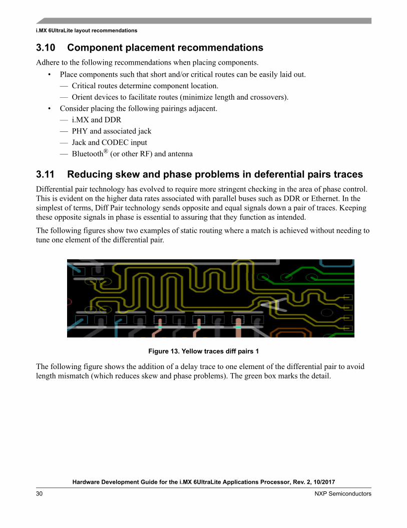
Differential pair technology has evolved to require more stringent checking in the area of phase control. This is evident on the higher data rates associated with parallel buses such as DDR or Ethernet. In the simplest of terms, Diff Pair technology sends opposite and equal signals down a pair of traces. Keeping these opposite signals in phase is essential to assuring that they function as intended.
The following figures show two examples of static routing where a match is achieved without needing to tune one element of the differential pair.
Figure 13. Yellow traces diff pairs 1
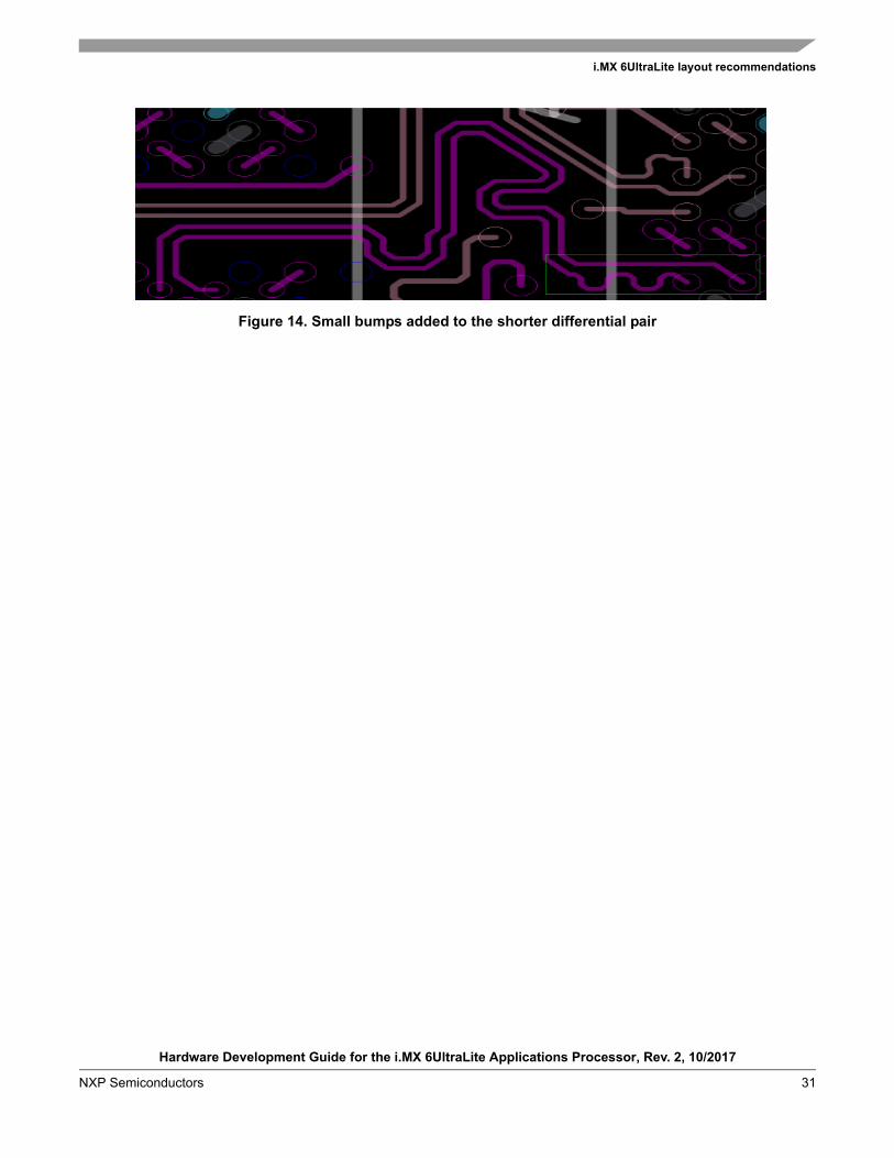
The following figure shows the addition of a delay trace to one element of the differential pair to avoid length mismatch (which reduces skew and phase problems). The green box marks the detail.
Hardware Development Guide for the i.MX 6UltraLite Applications Processor, Rev. 2, 10/2017
NXP Semiconductors 31
i.MX 6UltraLite layout recommendations
Figure 14. Small bumps added to the shorter differential pair
Hardware Development Guide for the i.MX 6UltraLite Applications Processor, Rev. 2, 10/2017
32 NXP Semiconductors
Avoiding board bring-up problems
4 Avoiding board bring-up problems
4.1 Introduction
This chapter provides recommendations for avoiding typical mistakes when bringing up a board for the first time. These recommendations consist of basic techniques that have proven useful in the past for detecting board issues and addressing the three most typical bring-up pitfalls: power, clocks, and reset. A sample bring-up checklist is provided at the end of the chapter.
4.2 Using a current monitor to avoid power pitfalls
Excessive current can cause damage to the board. Avoid this problem by using a current-limiting laboratory supply set to the expected typical main current draw (at most). Monitor the main supply current with an ammeter when powering up the board for the first time. You can use the supply's internal ammeter if it has one. By monitoring the main supply current and controlling the current limit, any excessive current can usually be detected before permanent damage occurs.
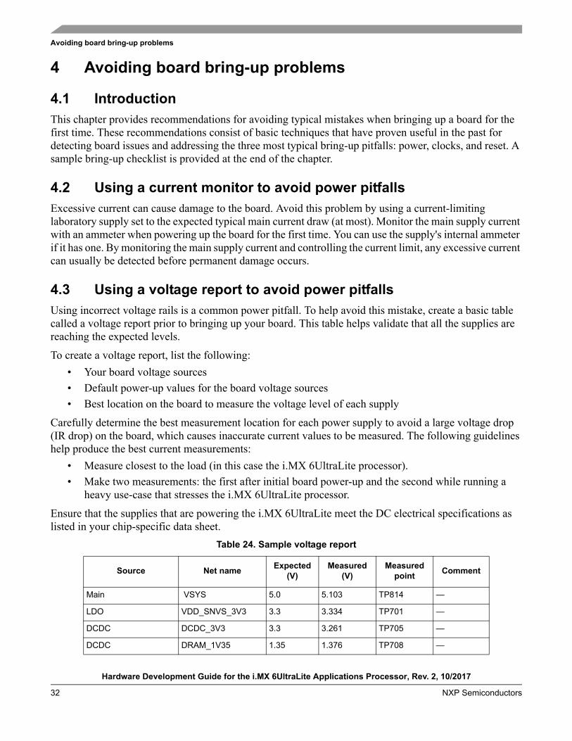
4.3 Using a voltage report to avoid power pitfalls
Using incorrect voltage rails is a common power pitfall. To help avoid this mistake, create a basic table called a voltage report prior to bringing up your board. This table helps validate that all the supplies are reaching the expected levels.
To create a voltage report, list the following:
• Your board voltage sources
• Default power-up values for the board voltage sources
• Best location on the board to measure the voltage level of each supply
Carefully determine the best measurement location for each power supply to avoid a large voltage drop (IR drop) on the board, which causes inaccurate current values to be measured. The following guidelines help produce the best current measurements:
• Measure closest to the load (in this case the i.MX 6UltraLite processor).
• Make two measurements: the first after initial board power-up and the second while running a heavy use-case that stresses the i.MX 6UltraLite processor.
Ensure that the supplies that are powering the i.MX 6UltraLite meet the DC electrical specifications as listed in your chip-specific data sheet.
Table 24. Sample voltage report
Source Net name Expected
(V) Measured
(V) Measured
point Comment
Main VSYS 5.0 5.103 TP814 —
LDO VDD_SNVS_3V3 3.3 3.334 TP701 —
DCDC DCDC_3V3 3.3 3.261 TP705 —
DCDC DRAM_1V35 1.35 1.376 TP708 —
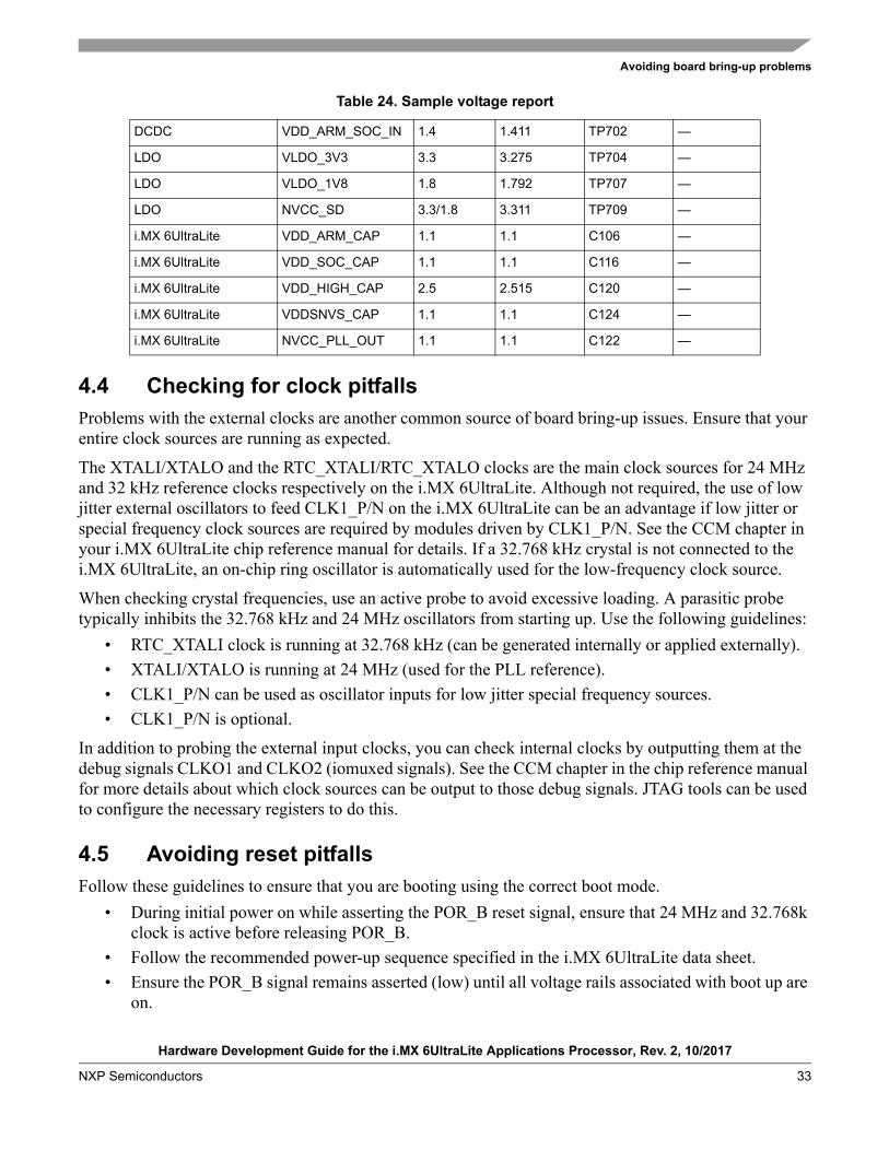
Hardware Development Guide for the i.MX 6UltraLite Applications Processor, Rev. 2, 10/2017
NXP Semiconductors 33
Avoiding board bring-up problems
4.4 Checking for clock pitfalls
Problems with the external clocks are another common source of board bring-up issues. Ensure that your entire clock sources are running as expected.
The XTALI/XTALO and the RTC_XTALI/RTC_XTALO clocks are the main clock sources for 24 MHz and 32 kHz reference clocks respectively on the i.MX 6UltraLite. Although not required, the use of low jitter external oscillators to feed CLK1_P/N on the i.MX 6UltraLite can be an advantage if low jitter or special frequency clock sources are required by modules driven by CLK1_P/N. See the CCM chapter in your i.MX 6UltraLite chip reference manual for details. If a 32.768 kHz crystal is not connected to the i.MX 6UltraLite, an on-chip ring oscillator is automatically used for the low-frequency clock source.
When checking crystal frequencies, use an active probe to avoid excessive loading. A parasitic probe typically inhibits the 32.768 kHz and 24 MHz oscillators from starting up. Use the following guidelines:
• RTC_XTALI clock is running at 32.768 kHz (can be generated internally or applied externally).
• XTALI/XTALO is running at 24 MHz (used for the PLL reference).
• CLK1_P/N can be used as oscillator inputs for low jitter special frequency sources.
• CLK1_P/N is optional.
In addition to probing the external input clocks, you can check internal clocks by outputting them at the debug signals CLKO1 and CLKO2 (iomuxed signals). See the CCM chapter in the chip reference manual for more details about which clock sources can be output to those debug signals. JTAG tools can be used to configure the necessary registers to do this.
4.5 Avoiding reset pitfalls
Follow these guidelines to ensure that you are booting using the correct boot mode.
• During initial power on while asserting the POR_B reset signal, ensure that 24 MHz and 32.768k clock is active before releasing POR_B.
• Follow the recommended power-up sequence specified in the i.MX 6UltraLite data sheet.
• Ensure the POR_B signal remains asserted (low) until all voltage rails associated with boot up are on.
DCDC VDD_ARM_SOC_IN 1.4 1.411 TP702 —
LDO VLDO_3V3 3.3 3.275 TP704 —
LDO VLDO_1V8 1.8 1.792 TP707 —
LDO NVCC_SD 3.3/1.8 3.311 TP709 —
i.MX 6UltraLite VDD_ARM_CAP 1.1 1.1 C106 —
i.MX 6UltraLite VDD_SOC_CAP 1.1 1.1 C116 —
i.MX 6UltraLite VDD_HIGH_CAP 2.5 2.515 C120 —
i.MX 6UltraLite VDDSNVS_CAP 1.1 1.1 C124 —
i.MX 6UltraLite NVCC_PLL_OUT 1.1 1.1 C122 —
Table 24. Sample voltage report
Hardware Development Guide for the i.MX 6UltraLite Applications Processor, Rev. 2, 10/2017
34 NXP Semiconductors
Avoiding board bring-up problems
The GPIOs and internal fuses control how the i.MX 6UltraLite boots. For a more detailed description about the different boot modes, see the system boot chapter of the chip reference manual.
4.5.1 Sample board bring-up checklist
Note that the checklist incorporates the recommendations described in the previous sections. Blank cells should be filled in during bring-up as appropriate.
Table 25. Board bring-up checklist
Checklist Item Details OwnerFindings &
status
Note: The following items must be completed serially.
1. Perform a visual inspection. Check major components to make sure nothing has been misplaced or rotated before applying power.
2. Verify all i.MX 6UltraLite voltage rails.
Confirm that the voltages match the data sheet’s requirements. Be sure to check voltages not only at the voltage source, but also as close to the i.MX 6UltraLite as possible (like on a bypass capacitor). This reveals any IR drops on the board that will cause issues later. Ideally all of the i.MX 6UltraLite voltage rails should be checked, but VDD_ARM_SOC_IN is particularly important voltages. These are the core logic voltages and must fall within the parameters provided in the i.MX 6UltraLite data sheet. VDD_SNVS_IN, NVCC_GPIO, and NVCC_DRAM are also critical to the i.MX 6UltraLite boot up.
3. Verify power-up sequence. Verify that power on reset (POR_B) is de-asserted (high) after all power rails have come up and are stable. See the i.MX 6UltraLite data sheet for details about power-up sequencing.
4. Measure/probe input clocks (32 kHz, 24MHz, others).
Without a properly running clock, the i.MX 6UltraLite will not function properly.
5. Check JTAG connectivity This is one of the most fundamental and basic access points to the i.MX 6UltraLite to allow the debug and execution of low level code.
Note: The following items may be worked on in parallel with other bring up tasks.
Access internal RAM. Verify basic operation of the i.MX 6UltraLite in system. Perform a basic test by performing a write-read-verify to the internal RAM. No software initialization is necessary to access internal RAM.
Hardware Development Guide for the i.MX 6UltraLite Applications Processor, Rev. 2, 10/2017
NXP Semiconductors 35
Avoiding board bring-up problems
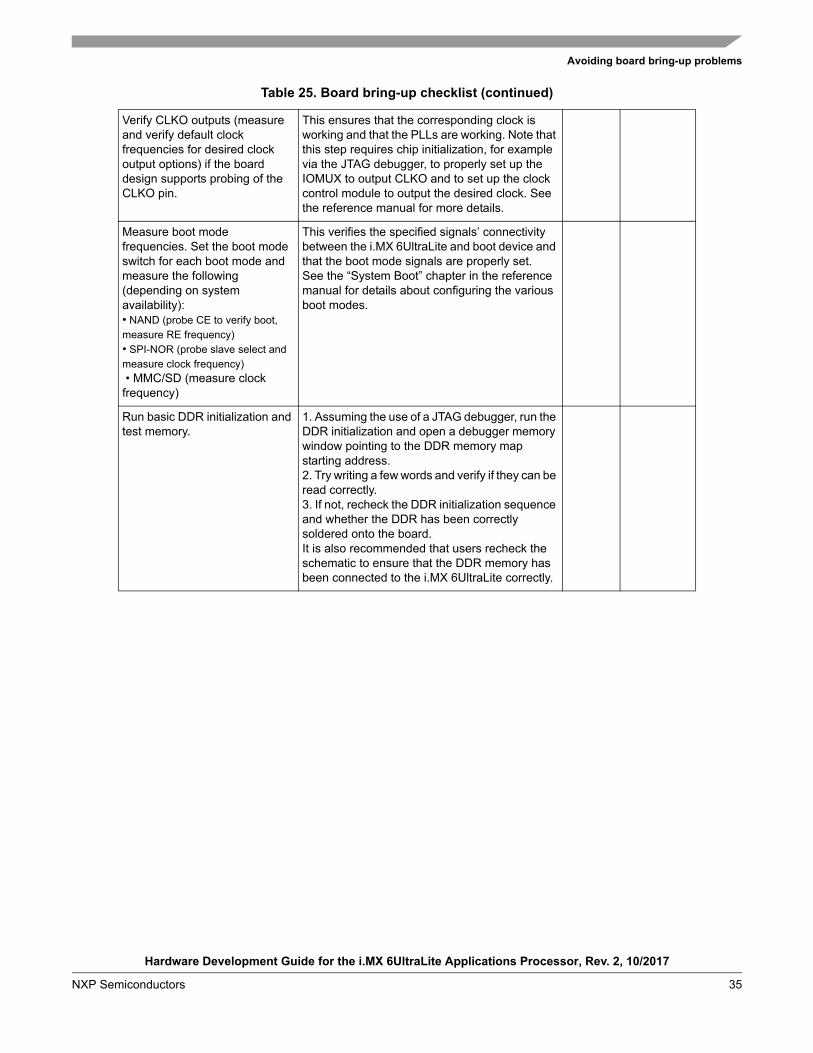
Verify CLKO outputs (measure and verify default clock frequencies for desired clock output options) if the board design supports probing of the CLKO pin.
This ensures that the corresponding clock is working and that the PLLs are working. Note that this step requires chip initialization, for example via the JTAG debugger, to properly set up the IOMUX to output CLKO and to set up the clock control module to output the desired clock. See the reference manual for more details.
Measure boot mode frequencies. Set the boot mode switch for each boot mode and measure the following (depending on system availability): • NAND (probe CE to verify boot, measure RE frequency) • SPI-NOR (probe slave select and measure clock frequency) • MMC/SD (measure clock frequency)
This verifies the specified signals’ connectivity between the i.MX 6UltraLite and boot device and that the boot mode signals are properly set.See the “System Boot” chapter in the reference manual for details about configuring the various boot modes.
Run basic DDR initialization and test memory.
1. Assuming the use of a JTAG debugger, run the DDR initialization and open a debugger memory window pointing to the DDR memory map starting address.2. Try writing a few words and verify if they can be read correctly.3. If not, recheck the DDR initialization sequence and whether the DDR has been correctly soldered onto the board.It is also recommended that users recheck the schematic to ensure that the DDR memory has been connected to the i.MX 6UltraLite correctly.
Table 25. Board bring-up checklist (continued)
Hardware Development Guide for the i.MX 6UltraLite Applications Processor, Rev. 2, 10/2017
36 NXP Semiconductors
Understanding the IBIS model
5 Understanding the IBIS model This chapter explains how to use the IBIS (input output buffer information specification) model, which is an Electronic Industries Alliance standard for the electronic behavioral specifications of integrated circuit input/output analog characteristics. The model is generated in ASCII text format and consists of multiple tables that capture current vs. voltage (IV) and voltage vs. time (VT) characteristics of each buffer. IBIS models are generally used to perform PCB-board-level signal integrity (SI) simulations and timing analyses.
The IBIS model’s features are as follows:
• Supports fast chip-package-board simulation, with SPICE-level accuracy and faster than any transistor-level model
• Provides the following for portable model data
— I/O buffers, series elements, terminators
— Package RLC parasitics
— Electrical board description
5.1 IBIS structure and content
An IBIS file contains the data required to model a component’s input, output, and I/O buffers behaviorally in ASCII format. The basic IBIS file contains the following data:
• Header information regarding the model file
Information about the component, the package’s electrical characteristics, and the pin-to-buffer model mapping (in other words, which pins are connected to which buffer models)
Τhe data required to model each unique input, output, and I/O buffer design on the component
IBIS models are component-centric, meaning they allow users to model an entire component rather than only a particular buffer. Therefore, in addition to the electrical characteristics of a component’s buffers, an IBIS file includes the component’s pin-to-buffer mapping and the electrical parameters of the component’s package.
5.2 Header Information
The first section of an IBIS file provides the basic information about the file and its data. The following table explains the header information notation.
Table 26. Header Information
Keyword Required Description
[IBIS Ver] Yes Version of IBIS Specification this file uses.
[Comment char] No Change the comment character. Defaults to the pipe (|) character.
[File Name] Yes Name of this file. All file names must be lower case. The file name extension for an IBIS file is .ibs.
Hardware Development Guide for the i.MX 6UltraLite Applications Processor, Rev. 2, 10/2017
NXP Semiconductors 37
Understanding the IBIS model
Example 1. Header Information
[IBIS Ver] 4.2
[Comment Char] |_char
[File Name] 14x14_imx6ul_autmtv_1.ibs
[File Rev] 001
[Date] Sat Jan 31 02:23:00 2015
[Source] FSL Viper 2012.03.14
[Notes]
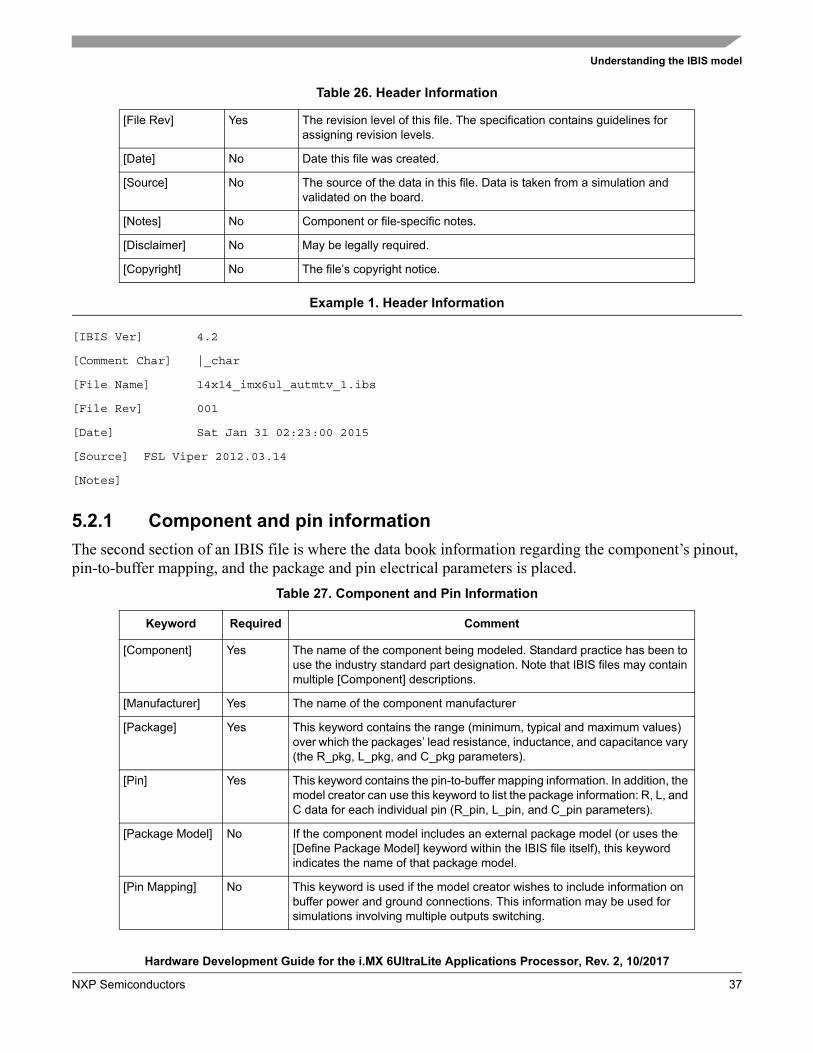
5.2.1 Component and pin information
The second section of an IBIS file is where the data book information regarding the component’s pinout, pin-to-buffer mapping, and the package and pin electrical parameters is placed.
[File Rev] Yes The revision level of this file. The specification contains guidelines for assigning revision levels.
[Date] No Date this file was created.
[Source] No The source of the data in this file. Data is taken from a simulation and validated on the board.
[Notes] No Component or file-specific notes.
[Disclaimer] No May be legally required.
[Copyright] No The file’s copyright notice.
Table 27. Component and Pin Information
Keyword Required Comment
[Component] Yes The name of the component being modeled. Standard practice has been to use the industry standard part designation. Note that IBIS files may contain multiple [Component] descriptions.
[Manufacturer] Yes The name of the component manufacturer
[Package] Yes This keyword contains the range (minimum, typical and maximum values) over which the packages’ lead resistance, inductance, and capacitance vary (the R_pkg, L_pkg, and C_pkg parameters).
[Pin] Yes This keyword contains the pin-to-buffer mapping information. In addition, the model creator can use this keyword to list the package information: R, L, and C data for each individual pin (R_pin, L_pin, and C_pin parameters).
[Package Model] No If the component model includes an external package model (or uses the [Define Package Model] keyword within the IBIS file itself), this keyword indicates the name of that package model.
[Pin Mapping] No This keyword is used if the model creator wishes to include information on buffer power and ground connections. This information may be used for simulations involving multiple outputs switching.
Table 26. Header Information
Hardware Development Guide for the i.MX 6UltraLite Applications Processor, Rev. 2, 10/2017
38 NXP Semiconductors
Understanding the IBIS model
Example 2. Component and pin information
[Component] mx6sx_bga19x19 [Manufacturer] FREESCALE [Package] | variable typ min max R_pkg 0.2839146 0.0091798 0.575946 L_pkg 3.33311nH 0.16746nH 7.75079nH C_pkg 24.5630pF 1.13795pF 356.1pF | [Pin] signal_name model_name R_pin L_pin C_pin A1 VSS GND NA NA NA A2 DRAM_SDQS3_N ddr 0.473559 5.48846nH 1.36964pF A3 DRAM_SDQS3_P ddr 0.478764 5.40998nH 1.61263pF
5.2.2 Model information
The [Model] keyword starts the description of the data for a particular buffer.
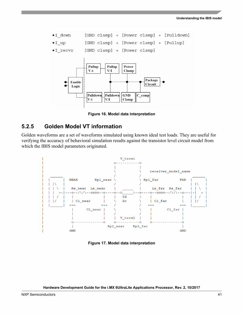
5.2.3 IV information
IV information is composed of four Current-over-Voltage tables: [Pullup], [Pulldown], [GND_clamp], and [Power_clamp]. Each look-up table describes a different part of the IO cell model.
[Diff Pin] No This keyword is used to associate buffers that should be driven in a complementary fashion as a differential pair.
[Model Selector] Yes This keyword provides a simple means by which several buffers can be made optionally available for simulation at the same physical pin of the component.
Table 28. Model information
Keyword Comment
[Model Spec] General set of parameters for the model simulation.
[Receiver Thresholds] Threshold information for the different simulation cases.
[Temperature Range] The temperature range over which the min, typ and max IV and switching data have been gathered.
[Voltage Range] The range over which Vcc is varied to obtain the min, typ and max pullup and power clamp data.
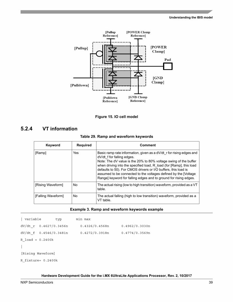
[Pulldown] [Pullup] [GND_clamp] [POWER_clamp]
IV information. For more details, see Section 5.2.3, “IV information.”
[Ramp] [Rising Waveform] [Falling Waveform]
VT information. For more details, see Section 5.2.4, “VT information.”
[Test Data] [Rising Waveform Near] [Rising Waveform Far] [Falling Waveform Near] [Falling Waveform Far] [Test Load]
VT golden model information. For more details, see Section 5.2.5, “Golden Model VT information.”
Table 27. Component and Pin Information
Hardware Development Guide for the i.MX 6UltraLite Applications Processor, Rev. 2, 10/2017
NXP Semiconductors 39
Understanding the IBIS model
Figure 15. IO cell model
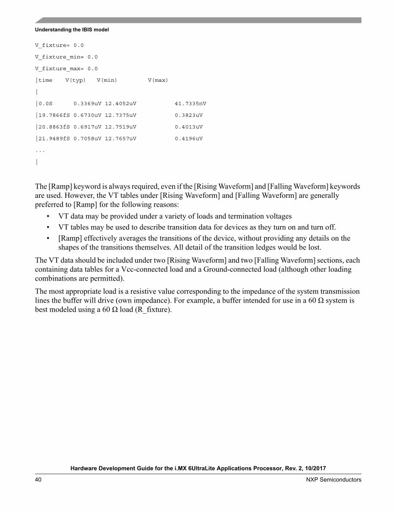
5.2.4 VT information
Example 3. Ramp and waveform keywords example
| variable typ min max
dV/dt_r 0.4627/0.3456n 0.4326/0.4568n 0.4962/0.3030n
dV/dt_f 0.4546/0.3481n 0.4272/0.3918n 0.4774/0.3569n
R_load = 0.2400k
|
[Rising Waveform]
R_fixture= 0.2400k
Table 29. Ramp and waveform keywords
Keyword Required Comment
[Ramp] Yes Basic ramp rate information, given as a dV/dt_r for rising edges and dV/dt_f for falling edges. Note: The dV value is the 20% to 80% voltage swing of the buffer when driving into the specified load, R_load (for [Ramp], this load defaults to 50). For CMOS drivers or I/O buffers, this load is assumed to be connected to the voltages defined by the [Voltage Range] keyword for falling edges and to ground for rising edges.
[Rising Waveform] No The actual rising (low to high transition) waveform, provided as a VT table.
[Falling Waveform] No The actual falling (high to low transition) waveform, provided as a VT table.
Hardware Development Guide for the i.MX 6UltraLite Applications Processor, Rev. 2, 10/2017
40 NXP Semiconductors
Understanding the IBIS model
V_fixture= 0.0
V_fixture_min= 0.0
V_fixture_max= 0.0
|time V(typ) V(min) V(max)
|
|0.0S 0.3369uV 12.4052uV 41.7335nV
|19.7866fS 0.6730uV 12.7375uV 0.3823uV
|20.8863fS 0.6917uV 12.7519uV 0.4013uV
|21.9489fS 0.7058uV 12.7657uV 0.4196uV
...
|
The [Ramp] keyword is always required, even if the [Rising Waveform] and [Falling Waveform] keywords are used. However, the VT tables under [Rising Waveform] and [Falling Waveform] are generally preferred to [Ramp] for the following reasons:
• VT data may be provided under a variety of loads and termination voltages
• VT tables may be used to describe transition data for devices as they turn on and turn off.
• [Ramp] effectively averages the transitions of the device, without providing any details on the shapes of the transitions themselves. All detail of the transition ledges would be lost.
The VT data should be included under two [Rising Waveform] and two [Falling Waveform] sections, each containing data tables for a Vcc-connected load and a Ground-connected load (although other loading combinations are permitted).
The most appropriate load is a resistive value corresponding to the impedance of the system transmission lines the buffer will drive (own impedance). For example, a buffer intended for use in a 60 Ω system is best modeled using a 60 Ω load (R_fixture).
Hardware Development Guide for the i.MX 6UltraLite Applications Processor, Rev. 2, 10/2017
NXP Semiconductors 41
Understanding the IBIS model
Figure 16. Model data interpretation
5.2.5 Golden Model VT information
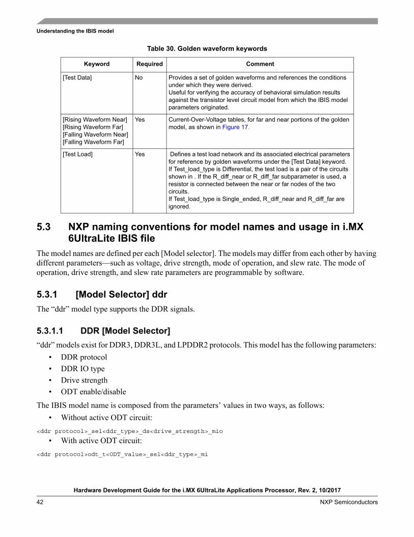
Golden waveforms are a set of waveforms simulated using known ideal test loads. They are useful for verifying the accuracy of behavioral simulation results against the transistor level circuit model from which the IBIS model parameters originated.
Figure 17. Model data interpretation
Hardware Development Guide for the i.MX 6UltraLite Applications Processor, Rev. 2, 10/2017
42 NXP Semiconductors
Understanding the IBIS model
5.3 NXP naming conventions for model names and usage in i.MX 6UltraLite IBIS file
The model names are defined per each [Model selector]. The models may differ from each other by having different parameters—such as voltage, drive strength, mode of operation, and slew rate. The mode of operation, drive strength, and slew rate parameters are programmable by software.
5.3.1 [Model Selector] ddr
The “ddr” model type supports the DDR signals.
5.3.1.1 DDR [Model Selector]
“ddr” models exist for DDR3, DDR3L, and LPDDR2 protocols. This model has the following parameters:
• DDR protocol
• DDR IO type
• Drive strength
• ODT enable/disable
The IBIS model name is composed from the parameters’ values in two ways, as follows:
• Without active ODT circuit:
<ddr protocol>_sel<ddr_type>_ds<drive_strength>_mio
• With active ODT circuit:
<ddr protocol>odt_t<ODT_value>_sel<ddr_type>_mi
Table 30. Golden waveform keywords
Keyword Required Comment
[Test Data] No Provides a set of golden waveforms and references the conditions under which they were derived. Useful for verifying the accuracy of behavioral simulation results against the transistor level circuit model from which the IBIS model parameters originated.
[Rising Waveform Near] [Rising Waveform Far] [Falling Waveform Near] [Falling Waveform Far]
Yes Current-Over-Voltage tables, for far and near portions of the golden model, as shown in Figure 17.
[Test Load] Yes Defines a test load network and its associated electrical parameters for reference by golden waveforms under the [Test Data] keyword.If Test_load_type is Differential, the test load is a pair of the circuits shown in . If the R_diff_near or R_diff_far subparameter is used, a resistor is connected between the near or far nodes of the two circuits. If Test_load_type is Single_ended, R_diff_near and R_diff_far are ignored.
Hardware Development Guide for the i.MX 6UltraLite Applications Processor, Rev. 2, 10/2017
NXP Semiconductors 43
Understanding the IBIS model
DDR write models ("_mio" suffix) have no simulated ODT, as ODT is disabled during write. Write models' DS parameter is meaningful and changes to describe the different levels of drive strength. DDR read models ("_mi" suffix) have no meaningful DS parameter, as no driving happens during read. Read models’ ODT parameter is meaningful and changes to describe different levels of ODT impedance.
Example 4. [Model Selector] DDR in IBIS file
ddr3_sel11_ds111_mio DDR, 1.5V, ddr3 mode, 34 Ohm driver impedance
…
lpddr2_sel10_ds111_mio LPDDR, 1.2V, lpddr2 mode, 34 Ohm driver impedance
…
——————————————————————————————————————————
See the register description in the IOMUXC chapter in the chip reference manual for further details about this model.
5.3.2 [Model Selector] GPIO
This model has the following parameters:
• Voltage level
• Drive strength
• Slew rate
• Speed
The IBIS model name is composed from parameters’ values as follows:
gpio<voltage_level>_ds<drive_strength>_sr<slew_rate(1 bit)><speed(2 bits)>_mio
Table 31. Module Selector Reference Guide for ddr
DDR Protocol Selected according to the used DDR. DDR IO voltage level is selected accordingly.
DDR IO TypeControlled by the IOMUXC_SW_PAD_CTL_GRP_DDR_TYPE[19:18] register in IOMUXC (IOMUX controller) DDR_SEL bits, to select between DDR3 & LPDDR2.
Drive strength
Controlled by bits [5:3] (DSE) of the following registers in IOMUX (IOMUX controller):IOMUXC_SW_PAD_CTL_GRP_BxDS (4 registers) IOMUXC_SW_PAD_CTL_GRP_CTLDS IOMUXC_SW_PAD_CTL_PAD_DRAM_ADDRxx (16 registers) IOMUXC_SW_PAD_CTL_PAD_DRAM_DQMx (4 registers) IOMUXC_SW_PAD_CTL_PAD_DRAM_RAS_B IOMUXC_SW_PAD_CTL_PAD_DRAM_CAS_B IOMUXC_SW_PAD_CTL_PAD_DRAM_CSx_B (2 registers) IOMUXC_SW_PAD_CTL_PAD_DRAM_SDWE_B IOMUXC_SW_PAD_CTL_PAD_DRAM_ODTx (2 registers) IOMUXC_SW_PAD_CTL_PAD_DRAM_SDBAx (3 registers) IOMUXC_SW_PAD_CTL_PAD_DRAM_SDCKE0 (2 registers) IOMUXC_SW_PAD_CTL_PAD_DRAM_SDCLK0_P IOMUXC_SW_PAD_CTL_PAD_DRAM_SDQS0_P (4 registers) IOMUXC_SW_PAD_CTL_PAD_DRAM_RESET
ODT valueControlled by bits [18:16], [14:12], [10:8], and [6:4] in MPODTCTRL register of MMDC.
Hardware Development Guide for the i.MX 6UltraLite Applications Processor, Rev. 2, 10/2017
44 NXP Semiconductors
Understanding the IBIS model
See the register description in the IOMUXC chapter in the chip reference manual for further details about this model.
5.4 Quality assurance for the IBIS models
The IBIS models are validated against the IBIS specification, which provides a way to objectively measure the correlation of model simulation results with reference transistor-level spice simulation or measurements.
Correlation: The process of making a quantitative comparison between two sets of I/O buffer characterization data, such as lab measurement vs. structural simulation or behavioral simulation vs. structural simulation.
Correlation: Level A means for categorizing I/O buffer characterization data based on how much the modeling engineer knows about the processing conditions of a sample component and which correlation metric he or she used.
All models have passed the following checks:
• IBISCHK without errors or unexplained warnings
• Data for basic simulation checked
• Data for timing analysis checked
• Data for power analysis checked
• Correlated against Spice simulations
5.5 IBIS usage
NXP board designers used the i.MX 6UltraLite IBIS model with the Hyperlynx tool by Mentor Graphics.
Effective board design results achieved after loading:
• i.MX 6UltraLite IBIS model.
• Companion IC IBIS models.
• Board model in HyperLynx format.
Board simulations for various GPIO and DDR signals were then run.
Table 32. Module Selector Reference Guide for GPIO
Voltage Level
For i.MX 6UltraLite chips, there are no user configurations for the voltage level because the GPIO cell senses the NVCC and auto-configures itself accordingly. The IBIS user can choose between high and low voltage by selecting a different model at [Model Selector].
Drive strengthControlled by the DSE bits (bits [5:3]) in theIOMUXC_SW_PAD_CTL_PAD_<pad name>.
Slew rateControlled by the SRE bit (bit 0) in the IOMUXC_SW_PAD_CTL_PAD_<pad name>.
SpeedControlled by the SPEED bits (bits [7:6]) in theIOMUXC_SW_PAD_CTL_PAD_<pad name>.
Hardware Development Guide for the i.MX 6UltraLite Applications Processor, Rev. 2, 10/2017
NXP Semiconductors 45
Understanding the IBIS model
5.6 References
Consult the following references for more information about the IBIS model.
• IBIS Open Forum (http://www.eda.org/ibis/) The IBIS Open Forum consists of EDA vendors, computer manufacturers, semiconductor vendors, universities, and end-users. It proposes updates and reviews, revises standards, and organizes summits. It promotes IBIS models and provides useful documentation and tools.
• IBIS specification (http://eda.org/pub/ibis/ver4.2/)
Hardware Development Guide for the i.MX 6UltraLite Applications Processor, Rev. 2, 10/2017
46 NXP Semiconductors
Using the manufacturing tool
6 Using the manufacturing tool
6.1 Overview
The i.MX manufacturing tool is designed to program firmware onto storage devices such as NAND or eSDe through the EVK and preload the data area with media files in an efficient and convenient manner. It is intended for NXP Semiconductors customers or their OEMs who plan to mass manufacture i.MX-based products.
The application is not designed to test the devices or to diagnose manufacturing problems. Devices initialized with this application still need to be functionally verified.
6.2 Feature summary
The tool includes the following features:
• Continuous operation—operations automatically begin with the connection of a new device, and multiple operations such as update and copy can be linked together seamlessly.
• Enumeration—static-ID firmware loaded into RAM in recovery-mode prevents Windows® from enumerating every device.
• AutoPlay—various Windows® ‘pop-up’ application and status messages, such as Explorer in Windows® XP and Windows 7.
In addition, the following characteristics improve the tool’s ease of use:
• An independent process bar is set up for each physical USB port.
• The tool begins processing with the connection of the first device detected and allows users to replace each device after completion instead of needing to wait for all devices to complete.
• The tool uses color-based indicators to indicate the work status on each of the ports.
— Blue indicates the device is being processed.
— Green indicates the device was successfully processed and that the programmed device can be replaced with a new one independent of the of the device’s progress.
— Red indicates the device failed to process.
6.3 Version support
6.4 Connecting the manufacturing tool to your device
The manufacturing tool can be connected using a USB hub-based physical setup or a direct connection, as described in Section 6.4.1, “Connecting with a USB hub,” and Section 6.4.2, “Connecting directly.”
Table 33. Version support
Tool Version requirement
i.MX 6UltraLite Manufacturing Tool for WinCE Version 2.3.2 or later
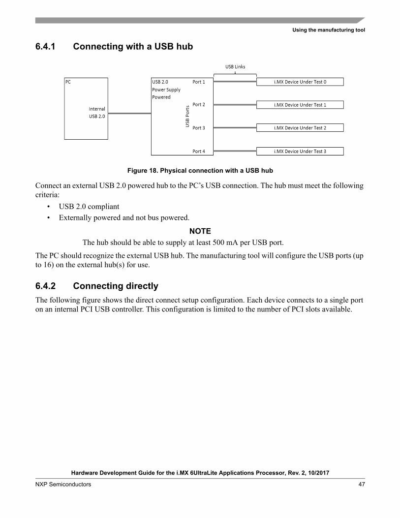
Hardware Development Guide for the i.MX 6UltraLite Applications Processor, Rev. 2, 10/2017
NXP Semiconductors 47
Using the manufacturing tool
6.4.1 Connecting with a USB hub
Figure 18. Physical connection with a USB hub
Connect an external USB 2.0 powered hub to the PC’s USB connection. The hub must meet the following criteria:
• USB 2.0 compliant
• Externally powered and not bus powered.
NOTE
The hub should be able to supply at least 500 mA per USB port.
The PC should recognize the external USB hub. The manufacturing tool will configure the USB ports (up to 16) on the external hub(s) for use.
6.4.2 Connecting directly
The following figure shows the direct connect setup configuration. Each device connects to a single port on an internal PCI USB controller. This configuration is limited to the number of PCI slots available.

Hardware Development Guide for the i.MX 6UltraLite Applications Processor, Rev. 2, 10/2017
48 NXP Semiconductors
Using the manufacturing tool
Figure 19. Physical connection without a USB hub
6.5 Installing the manufacturing tool
The following subsections explain how to install the manufacturing tool. These subsections are in chronological order.
6.5.1 Running the .exe
The following steps explain where to install the .exe. This executable can be run directly and requires no special installation.
1. Unzip the tool package to your local directory (for example, D:\mfgtools-rel\).
2. Find MfgTool.exe in the list of files.
3. Run MfgTool.exe in your local directory.
You should see a user interface similar to the one shown in the following figure.
Figure 20. Example user interface
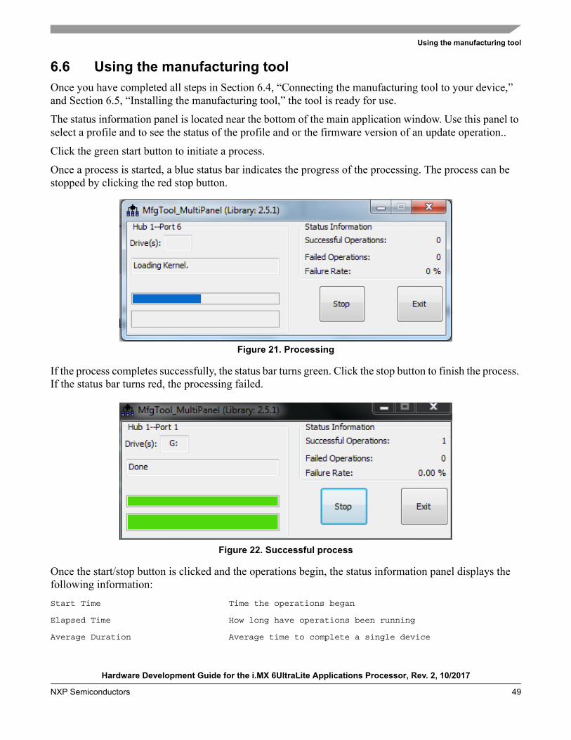
Hardware Development Guide for the i.MX 6UltraLite Applications Processor, Rev. 2, 10/2017
NXP Semiconductors 49
Using the manufacturing tool
6.6 Using the manufacturing tool
Once you have completed all steps in Section 6.4, “Connecting the manufacturing tool to your device,” and Section 6.5, “Installing the manufacturing tool,” the tool is ready for use.
The status information panel is located near the bottom of the main application window. Use this panel to select a profile and to see the status of the profile and or the firmware version of an update operation..
Click the green start button to initiate a process.
Once a process is started, a blue status bar indicates the progress of the processing. The process can be stopped by clicking the red stop button.
Figure 21. Processing
If the process completes successfully, the status bar turns green. Click the stop button to finish the process. If the status bar turns red, the processing failed.
Figure 22. Successful process
Once the start/stop button is clicked and the operations begin, the status information panel displays the following information:
Start Time Time the operations began
Elapsed Time How long have operations been running
Average Duration Average time to complete a single device
Hardware Development Guide for the i.MX 6UltraLite Applications Processor, Rev. 2, 10/2017
50 NXP Semiconductors
Using the manufacturing tool
Successful Operations How many devices successfully updated
Failed Operations How many device updates have failed
Failure Rate Percentage of failures
If you have a terminal tool to monitor the debug serial port of your board, you can open it to see more process information than what is presented in the GUI.
6.7 Customizing the manufacturing tool
This chapter illustrates the tool’s behavior with screenshots from the reference design boards provided by NXP. However, you can customize the tool for other designs. For detailed information on customizing the manufacturing tool, see the Manufacturing Tool User’s Manual.
6.8 Other references
For more detailed information about the manufacturing tool, see the following documents included in the manufacturing tool release package. Contact your local NXP sales office for assistance obtaining documents if needed:
• For detailed information about how to use the manufacturing tool, see Manufacturing Tool V2 Quick Start Guide.
• For detailed information about how to script the processing operations of the manufacturing tool, see the Manufacturing Tool V2 UCL User Manual.
• For information about how to generate the manufacturing tool firmware for Linux and Android, see Manufacturing Tool V2 Linux or Android Firmware Development Guide.
• For the change list and known issues, see Manufacturing Tool V2 Release Notes.
Hardware Development Guide for the i.MX 6UltraLite Applications Processor, Rev. 2, 10/2017
NXP Semiconductors 51
Using BSDL for board-level testing
7 Using BSDL for board-level testing
7.1 BSDL overview
Boundary scan description language (BSDL) is used for board-level testing after components have been assembled. The interface for this test uses the JTAG pins. The definition is contained within IEEE Std 1149.1.
7.2 How BSDL functions
A BSDL file defines the internal scan chain, which is the serial linkage of the IO cells, within a particular device. The scan chain looks like a large shift register, which provides a means to read the logic level applied to a pin or to output a logic state on that pin. Using JTAG commands, a test tool uses the BSDL file to control the scan chain so that device-board connectivity can be tested.
For example, when using an external ROM test interface, the test tool would do the following:
1. Output a specific set of addresses and controls to pins connected to the ROM
2. Perform a read command and scan out the values of the ROM data pins.
3. Compare the values read with the known golden values.
Based on this procedure, the tool can determine whether the interface between the two parts is connected properly and does not contain shorts or opens.
7.3 Downloading the BSDL file
The BSDL file for each i.MX processor is stored on the NXP website upon product release. Contact your local sales office or fields applications engineer to check the availability of information prior to product releases.
7.4 Pin coverage of BSDL
Each pin is defined as a port within the BSDL file. You can open the file with a text editor (like Wordpad) to review how each pin will function. The BSDL file defines these functions as shown:
-- PORT DESCRIPTION TERMS
-- in = input only
-- out = three-state output (0, Z, 1)
-- buffer = two-state output (0, 1)
-- inout = bidirectional
-- linkage = OTHER (vdd, vss, analog)
The appearance of ”linkage” in a pin’s file implies that the pin cannot be used with boundary scan. These are usually power pins or analog pins that cannot be defined with a digital logic state.

Hardware Development Guide for the i.MX 6UltraLite Applications Processor, Rev. 2, 10/2017
52 NXP Semiconductors
Using BSDL for board-level testing
7.5 Boundary scan operation
The boundary scan operation is controlled by:
• TEST_MODE, POR_B, and JTAG_MOD pins
• On-chip Fuse bits
The JTAG_MOD pin state controls the selection of JTAG to the core logic or boundary scan operation. See the following references for further information:
• The “System JTAG Controller (SJC)” chapter in the chip reference manual for the definitions of the JTAG interface operations.
• The “JTAG Security Modes” section in the same chapter for an explanation of the operation of the e-Fuse bit definitions in the following table.
• The “Fusemap” chapter in the chip reference manual the fusemap tables.
7.6 I/O pin power considerations
The boundary scan operation uses each of the available device pins to drive or read values within a given system. Therefore, the power supply pin for each specific module must be powered in order for the IO buffers to operate. This is straightforward for the digital pins within the system.
PCIe is not a digital interface, but the module provides built-in support for the IEEE 1149.6 extension for AC testing of their pins. Therefore, this module must also be powered when utilizing a scan chain that contains the pins from this module, or the scan chain does not function properly.
Table 34. System considerations for BSDL
Pin name Logic state Description
JTAG_MOD 1 IEEE 1149.1 JTAG compliant mode
BOOT_MODE[1:0] [0:0] [0:1] [1:0] Boot From Fuses Serial Downloader Internal Boot (Development)
POR_B 1 Power On Reset for the device
e-Fuse bits
JTAG_SMODE[1:0] [0:0] [0:1] JTAG enable mode Secure JTAG mode
SJC_DISABLE 0 Secure JTAG Controller is enabled
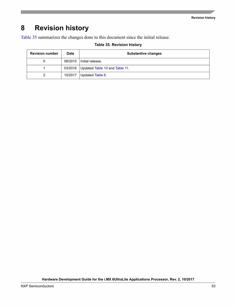
Hardware Development Guide for the i.MX 6UltraLite Applications Processor, Rev. 2, 10/2017
NXP Semiconductors 53
Revision history
8 Revision historyTable 35 summarizes the changes done to this document since the initial release.
Table 35. Revision history
Revision number Date Substantive changes
0 08/2015 Initial release.
1 03/2016 Updated Table 10 and Table 11.
2 10/2017 Updated Table 6.
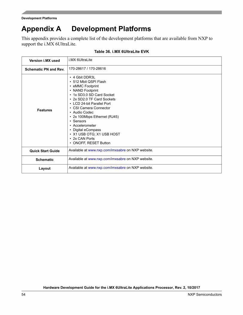
Hardware Development Guide for the i.MX 6UltraLite Applications Processor, Rev. 2, 10/2017
54 NXP Semiconductors
Development Platforms
Appendix A Development Platforms This appendix provides a complete list of the development platforms that are available from NXP to support the i.MX 6UltraLite.
Table 36. i.MX 6UltraLite EVK
Version i.MX used i.MX 6UltraLite
Schematic PN and Rev. 170-28617 / 170-28616
Features
• 4 Gbit DDR3L • 512 Mbit QSPI Flash • eMMC Footprint • NAND Footprint • 1x SD3.0 SD Card Socket • 2x SD2.0 TF Card Sockets • LCD 24-bit Parallel Port • CSI Camera Connector • Audio Codec • 2x 100Mbps Ethernet (RJ45) • Sensors • Accelerometer • Digital eCompass • X1 USB OTG; X1 USB HOST • 2x CAN Ports • ONOFF, RESET Button
Quick Start Guide Available at www.nxp.com/imxsabre on NXP website.
Schematic Available at www.nxp.com/imxsabre on NXP website.
Layout Available at www.nxp.com/imxsabre on NXP website.
Document Number: IMX6ULHDGRev. 2
10/2017
Information in this document is provided solely to enable system and software
implementers to use NXP products. There are no express or implied copyright licenses
granted hereunder to design or fabricate any integrated circuits based on the
information in this document. NXP reserves the right to make changes without further
notice to any products herein.
NXP makes no warranty, representation, or guarantee regarding the suitability of its
products for any particular purpose, nor does NXP assume any liability arising out of
the application or use of any product or circuit, and specifically disclaims any and all
liability, including without limitation consequential or incidental damages. "Typical"
parameters that may be provided in NXP data sheets and/or specifications can and do
vary in different applications, and actual performance may vary over time. All operating
parameters, including "typicals," must be validated for each customer application by
customer's technical experts. NXP does not convey any license under its patent rights
nor the rights of others. NXP sells products pursuant to standard terms and conditions
of sale, which can be found at the following address:
nxp.com/SalesTermsandConditions.
How to Reach Us:Home Page: nxp.com
Web Support: nxp.com/support
NXP, the NXP logo, NXP SECURE CONNECTIONS FOR A SMARTER WORLD,
Freescale, and the Freescale logo are trademarks of NXP B.V. All other product or
service names are the property of their respective owners.
Arm, the Arm logo, and Cortex are registered trademarks of Arm Limited (or its
subsidiaries) in the EU and/or elsewhere. All rights reserved.
© 2015-2017 NXP B.V.