hardware scheduler for quad core...
TRANSCRIPT

Page 1
Hardware Scheduler for Quad Core Multiprocessor Idan Regev and Noy Nakash
Supervisor: Jose Yallouz
VLSI Laboratory, Dept. of Electrical Engineering.
Technion – Israel Institute of Technology
1. Background
In the recent years the research and development of single core performance hit the
performance wall. This wall is mainly due to limited instruction level parallelism,
practical limits to number of pipelining stages and a power ceiling due to cooling
limitations. This problem led to a radical change in the design of the architectures of
microprocessors. Theoretical analysis and performance evaluations showed that the
best way to realize performance improvement in accordance with Moore’s was to
move from complex uni-core processors to multicore processors based on much
simpler cores.
During the execution of a program, it is necessary to perform both processes and
data synchronization. Processes synchronization ensures that multiple threads or
processes that share a logical address space are simultaneously executed in an
orderly manner. Data synchronization ensures that multiple copies of data are kept
coherent with one another. The basic purpose of process synchronization is to
maintain data consistency.
In the world of uni-core processors the scheduling task is relatively simple and is
implemented in software and does not require too much execution time on the CPU.
In modern chip multiprocessor (CMP) systems, the scheduling of processes or
threads to symmetric or asymmetric cores is performed by the operating system.
This is a complex and time consuming task which incurs a significant performance
penalty. The main idea of this project was to develop a hardware scheduler that
could replace most of the functions performed by the software scheduler of the
operating system. As the hardware can closely monitor the execution and therefore
the completion of processes, it is reasonable to expect that a hardware scheduler
would be capable of performing the scheduling tasks in a much simpler and clearly
much faster manner. Clearly this is in addition to the fact that hardware execution is
must faster that software in general. An additional requirement of the project was to
provide an interface between the operating system and the hardware scheduler.
This interface is implemented by the expansion the instruction set with new S-Type
instructions. The importance of this interface between the operating system and the
hardware scheduler is due to the fact that only the operating system knows which
process has the higher execution priority. The hardware has no way of knowing the
preferences of the system and the user so a means must be provided to transfer this
information from the application to the hardware.

Page 2
2. Problem Description
The ideal speed up of a CMP is equal to the number of cores. However it is
impossible to achieve this speedup for many reasons. Below is a list of factors which
limit the performance boost of the system. The solution presented in this paper
attempts to overcome these limitations as much as possible.
2.1 Limits of Speedup Factor
Amdahl's law states that the performance improvement to be gained from using
parallel execution is limited by the fraction of the time it takes to execute the serial
part of the code:
Amdahl law defines the speedup of a system with the following equation:
#
serial parallel
speedupparallel
serial overhead
t tT
tt
corest
+=
+ +
The process scheduling is always part of the serial code. If a mechanism that speeds
up scheduling can be implemented, it will often lead to a significant improvement in
the speedup attainable by the system.
2.2 Process and Thread Scheduling and Dispatching
In current systems, process/thread scheduling and dispatching is performed by the
operating system. Each process has a process descriptor (PCB) and a signal vector in
the kernel memory space. The PCB holds an FSM for the process defining its state
(wait, enabled, etc). The signal vector is a set of signals for each process (ctrl C for
example). When a signal is received by the process, is runs the respective signal
handler which may influence that FSM of the process.
On every OS tick, an interrupt causes the operating system scheduler (OSS) to be
invoked. The scheduler then selects which of the enabled processes/threads are to
be dispatched for execution on the cores on the next time slot. The dispatcher then
performs a context switch for all new processes and threads. Reducing the number
of calls to the OSS, will reduce the number of context switches required.
2.3 Process and Thread Synchronization
A common way of synchronizing processes is using fork and join commands. These
commands are internally implemented in the OS using semaphores (mutexes). All
Execution time
Parallel time
Serial time
Page 3
accesses to semaphores are performed in kernel mode and therefore require
context switches. In addition, accesses to semaphores are memory accesses which
can be time consuming. If we can reduce or avoid the use of semaphores, we reduce
the number of time consuming context switches and memory accesses.
2.4 OS Signaling and Interrupts
In current systems, when a process terminates before the next OS tick, it sends an
interrupt that invokes the OS which causes a switch to kernel mode. In the proposed
solution, new S-type commands will signal a HW scheduler (HSW) to remove
dependency and save the context switch. The new system will not switch from user
mode to kernel mode when running an S-Type command. In addition, on every OS
tick an interrupt will cause the operating system scheduler to send up to 16
process/threads to the HWS. The HWS will create a dependency table using the
dependency information in each process. Using this information it will select the
enabled processes for dispatching. The HWS will also directly receive process
completion signals and will use them to update the dependency table which allows
very fast dispatch of newly enabled processes.
2.5 Thread Assignment to Specific Cores
1. Currently, processes/threads are arbitrarily assigned to cores. If consecutive
executions of a thread can be assigned to the same core, it is possible get better
cache hit rates as the cache may still contain the process'/thread's data.
2. In Windows, threads are arbitrarily assigned to cores. If the threads of the same
process can be assigned to the same core, it is possible get better cache hit rates as
the cache may still contain the process'/thread's data.
In order to support the above, the kernel needs to be modified and recompiled. An
alternative would be to use the proposed scheduler with small adaptations to
support this sort of scheduling.
3. Goals and Solutions
The goals of this project are derived from the issues stated above and are aimed at
significantly reducing scheduling overhead in multicore processors. These goals
include:
• Speeding up scheduling by performing many functions in hardware rather
than in software.
• Speeding up parallel programs by significantly reducing overhead when
scheduling the processes on the different cores of the processor.
• Enabling easy transfer existing programs for efficient execution on highly
parallel computing systems by modifying only the compiler and not the code
itself.

Page 4
• Helping the operating system to maintain concurrency between multi
processes applications.
• Simplifying data synchronization (coherency) mechanisms.
• Designing and implementing a quad core multiprocessor with a micro
architecture as described below.
3.1 Solution Description
In order to demonstrate the capabilities of the new hardware scheduler, a suitable
platform was needed. For this purpose, it was decided to design and implement a
quad core RISC microprocessor. In the next section, the processor architecture will
be described. This is followed by a section on the hardware scheduler that includes
an explanation of both the extended instruction set and the hardware module.
3.2 A Quad Core RISC Processor (QCRP) Architecture
The QCRP processor architecture is a 16-bit architecture with the following features:
Macro architecture
• 16-bit ISA of 16 instructions
• All instructions are executed in 5 cycles
• 16 registers for each core
• 16-bit Memory space
• Separate caches for instructions and data
FIG 2 : QUAD CORE ARCHITECTURE
Micro architecture
• In order execution
• Only one memory access per
cycle
• Instruction Misses
• Memory Misses

Page 5
3.3 Instruction Set Format
The processor is based on a RISC architecture using 16 bit data and instructions. The
processor implements an instruction set of 16 instructions divided into 4 basic types,
namely R-Type, 9 and 12 bit immediate I-Type and J-Type, each with a different
instruction format. In addition, a completely new S-Type instruction was designed
and implemented to couple the software, namely the processes from the compiler
stage and the operating system scheduling services to the hardware namely the
hardware scheduler and all general purpose cores.
R-TYPE:
Opcode Destination Target Src
[15..12] [11..8] [7:4] [3:0]
I-TYPE: (4 BITS IMMEDIATE)
Opcode Destination Target Imm
[15..12] [11..8] [7:4] [3:0]
I-TYPE: (9 BITS IMMEDIATE)
Opcode
[15..12]
Destination
[11..8]
Imm
[7..0]
J-TYPE: (12 BITS IMMEDIATE)
Opcode
[15..12]
Target
[11:0]
S-TYPE: (4 BITS FUNCTION)
Opcode Process ID Process rt function
[15..12] [11..8] [7:4] [3:0]
Table 1 : Instruction Format
3.4 The Hardware Scheduler
The new approach developed here provides an interface between the operating
system and the processor's hardware. This interface was implemented by two main
components. The first included expansion the instruction set with new S-Type
instructions and second included a hardware module (scheduler) whose task was to
make use of the data supplied by the S-Type commands to schedule and dispatch the
processes for execution.
Page 6
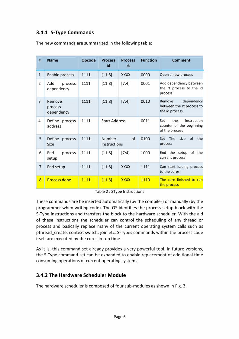
3.4.1 S-Type Commands
The new commands are summarized in the following table:
Comment Function Process
rt
Process
id
Opcode Name #
Open a new process 0000 XXXX [11:8] 1111 Enable process 1
Add dependency between
the rt process to the id
process
0001 [7:4] [11:8] 1111 Add process
dependency
2
Remove dependency
between the rt process to
the id process
0010 [7:4] [11:8] 1111 Remove
process
dependency
3
Set the instruction
counter of the beginning
of the process
0011 Start Address 1111 Define process
address
4
Set The size of the
process
0100 Number of
Instructions
1111 Define process
Size
5
End the setup of the
current process
1000 [7:4] [11:8] 1111 End process
setup
6
Can start issuing process
to the cores
1111 XXXX [11:8] 1111 End setup 7
The core finished to run
the process
1110 XXXX [11:8] 1111 Process done 8
Table 2 : SType Instructions
These commands are be inserted automatically (by the compiler) or manually (by the
programmer when writing code). The OS identifies the process setup block with the
S-Type instructions and transfers the block to the hardware scheduler. With the aid
of these instructions the scheduler can control the scheduling of any thread or
process and basically replace many of the current operating system calls such as
pthread_create, context switch, join etc. S-Types commands within the process code
itself are executed by the cores in run time.
As it is, this command set already provides a very powerful tool. In future versions,
the S-Type command set can be expanded to enable replacement of additional time
consuming operations of current operating systems.
3.4.2 The Hardware Scheduler Module
The hardware scheduler is composed of four sub-modules as shown in Fig. 3.

Page 7
FIG 3 : HARDWARE SCHEDULER
The scheduler control fsm builds the process and processes dependencies table and
decides which of next process can be issue to the cores. A core monitor fsm
maintains the real time cores working states and decides to which core to dispatch
the ready to run process. The dispatcher fsm controls the reset and init sequence in
order to run the process on the chosen core. The cores wrapper is responsible for
sending feedback on the processes status to the scheduler control fsm regarding
which process has completed.
The above four FSMs that control the flow of the scheduler mechanism, work in
parallel and the control between them is performed in a cyclic fashion from one fsm
to the next.
Three fsms perform operational tasks and one is a feedback fsm that together allow
the scheduler to issue processes to the designated cores in only 4 clock cycles. The
scheduler control fsm has 3 states:
Wait State
The scheduler waits for processes to arrive and the rest to de-assert (the bios finish
and the processor is "ready" to start running.

Page 8
Configuration State
The scheduler reads the setup block and creates a process dependency table (see
below) with all of the information it needs to schedule the process between the
cores. The programmer will have to write the instructions in the setup code as
follow:
1. Number of processes needed
2. Start process configuration
3. Dependency of the process on other processes
4. Start address of the process
5. End process configuration
6. Next process configuration
7. Repeat the 2-5 for all processes
8. End of setup block
Run State
The scheduler handler uses the processes table to decide which process is ready for
execution according to its own dependencies and priorities. When the process has
completed the scheduler receives an interrupt and updates the dependencies
accordingly. The scheduler then issues a new process to the free core. The
application code must be written according to the parallel coding guides.
3.3.3 Scheduler Unit Interface
Name IO To/From Description
clk in test Core clock
rst in test Core reset
init In test Instruction cache
core_instruction in Core Core finish signal
core_rst out Core Reset the core
core_init out Core Send the instructions cache to the cores

Page 9
3.4.3 Scheduler Setup Block Example
New process 0
Add process 1 dependency to process 0
Add process 2 dependency to process 0
O
O
O
Define process 0 address A
New process 1
Add process 2 dependency to process 0
Define process address B
New process 2
O
Define process address C
End setup
Rest of the program
TABLE 3 : DEPENDENCY INSTRUCTIONS
The dynamic data is stored in a cache as described below
Process
address
Dependency Process Enable
process
Process
Number
A 2 1 1 0
B 1 1 1
C 1 2
0 3
0 4
TABLE 4 : DEPENDENCY TABLE
The scheduler receives the information from the execution of the S-Type instructions
(table 3) and generates the process dependency data (table 4). It uses this
information to decide which processes can be dispatched in each execution time
slot.
3.5 Cache Architecture and Coherency Protocol
Every core has its own instruction cache and its own separate data cache. All four L1
caches are connected to a shared L2 cache. A coherency mechanism was
implemented in the form of a BUS controller with TDM arbitration that synchronizes
between the cores' L1 caches, L2 cache and the main memory. The diagram below
shows the system architecture. It can be seen that each core is connected only to its
own L1 cache and all the L1 caches are connected to the L2 (shared) cache, the
coherency mechanism is connected to all of the caches.

Page 10
FIGURE 4 – COHERENCY MECHANISM
3.5.1 Level 1 Cache
Every core can access the cache every cycle. Each L1 cache connected to the L2
cache by MSI Inclusive protocol. The L1 cache has a hit latency of 3 cycles. The L1
cache can submit an L2 cache request every cycle but will be granted access only
every 1/#cores because of the TDM mechanism. The data is temporary stored in a
designated FIFO stack.
3.5.2 Level 2 Cache
The L2 cache is connected to all the L1 caches. Although its read and writes latency is
higher than that of the L1 cache, it is bigger and can share data between the cores
without writing the data to the main memory.
3.5.3 Cache Coherency Protocol and Logic Implementation
The cache coherency protocol chosen for this CPU is MSI (Modified, Shared, Invalid).
The coherency mechanism is responsible for:
• Importing all the data from the L2 to the L1 and reverse.

Page 11
• Snooping repeatedly and changing the MSI bits in each cache according the
states.
• Controlling the Memory Bus.
3.5.3.1 MSI Protocol State Machines
The figure below show the MSI state machines for both CPU and Bus requests :
FIG 5 : MSI FSM FOR CPU REQUESTS MSI FSM FOR BUS REQUESTS
The operation of these two FSMs guarantees that the data in the caches is coherent
and that the CPU reads correct data. Although this is a standard and well known
protocol, its design and implementation presented in this work is very different from
existing implementations.
3.5.4.2 Snooping Process and Arbitration Protocol
Most snoopy cache mechanisms require on a common memory bus in order to
obtain the snoop data. As no suitable memory bus exists in this system, a feedback
path was implemented so all L1 caches could track all memory transactions. The L2
cache snoops each L1 cache separately and stores all of its calls in fifos, one FIFO for
MSI coherency calls (e.g. READ_MISS, WRITE_MISS etc) and one FIFO for the actual
data. This information is then fed back to all the other L1 caches.
Inside the L2 cache an arbiter divides the time slots among the L1 caches and every
clock checks the MSI and data FIFOs. If they are not empty, it pops the data from the
fifos and transfers it to the L2 and also to all of the other caches. Thus it typically
takes about 6 clock cycles to transfer data from one L1 to another. The compiler
should clearly be aware of this mechanism and should set dependencies between
the processes in the scheduler setup block accordingly.

Page 12
FIGURE 6 – CACHE LEVEL TWO BUS FIFOS MECHANISM
The "Time Division Multiplex" mechanism was designed to serialize L2 transactions
that may arrive in parallel to the four FIFOs. Each core is assigned a specific time slot
to transfer data to or from the L2. This protocol ensures that 2 cores cannot write to
the same address at once and prevents “race situation” problems among the cores.
The only scenario that the programmer needs to take care of is when two processes
must write to the same address in a particular order. As the order cannot be
guaranteed by the system, the programmer must add corresponding process S-Type
dependency instructions to ensure the order of dispatch of the processes will be as
required.
4. Performance Evaluation and Simulations
This new hardware scheduler will provide a significant performance gain by reducing
the number of context switches and memory accesses required for the following
scenarios:
a. Where use of S-Type instructions can replace current mechanisms for
implementing operations such as pthread_create, fork, join, etc.
b. Where use of S-Type instructions can replace current mechanisms that
require the use of semaphores.
Performing accurate performance evaluations for this system is a complex task and
beyond the scope of this project. In order to have some sort of estimates of the
expected gain one must use tools like those provided by the SimpleScalar tool set

Page 13
which provides an easily extensible, portable, high-performance test bed for system
performance evaluation. The work presented [1] showed that run time improves by
3 orders of magnitude and energy saving by 5 orders of magnitude if hardware
scheduling is used instead of software scheduling. In addition, it has been shown [3]
that thousands of clock cycles are required to perform context switches from user to
kernel modes in modern microprocessors.
The aim of the simulations performed in this work was to verify the correct
functionality of the design. Test programs were created and run to verify correctness
of the various features, mainly changing work load or number of threads and
different combinations of data dependencies to verify the correct functionality of the
MSI protocol. For example, a testbench that computes that scalar product of two
vectors was run to verify that the programmer was able to use S-Type instructions to
define dependency of the processes as needed and the hardware scheduler
interpreted that data correctly. This testbench also exercised the cache coherency
mechanism. In all the cases the whole system functioned as expected.
5. Synthesis and Layout Design
F I G U R E 7 – L A Y O U T
6. Challenges and Achievements
Not many publications were found on hardware scheduling. The work presented in
[2] deals with the implementation of a hardware scheduler, however the design does
not support the definition of process dependencies.
The main challenge and original contribution of this project was to design a new
paradigm for process scheduling in multicore processors. The lack of material in this
area meant that the complete concept had to be developed from scratch. Our
scratchpad was erased many times before the ideas presented in this work
materialized. The main achievements include:
The synthesis is the process in which an HDL
description of the design is converted into a
gate level implementation.
In this work the VHDL code was synthesized
using the Synopsys Design Analyzer and
using the TOWER 18um standard cell
libraries.
The layout shown in Fig. 7 was
implemented using the Cadence Encounter
tool. The figure shows the layout after floor
planning, standard cell placement and final
routing of the complete processor.

Page 14
• The development, design and implementation of a completely new process
scheduling paradigm that combines the use of new S-Type instructions and a
hardware scheduling module.
• The design and implementation of a complete quad core RISC processor
suitable to be used as a platform for the hardware scheduler.
• A new architecture was designed for implementing the MSI cache coherency
protocol for then multicore system.
• Targeting Amdahl’s law to the serial part of the code where it is harder to
squeeze more performance out of the system.
• Inventing every new S-type instruction in a way that future compilers could
add them to existing code simply by recompilation.
• Provide a HW scheduler that can be expanded to perform even more tasks
which are currently performed by the OS scheduler.
Future Research Fields
The designed scheduler provides solutions to some of the problems that exist in
current computer systems. Below is a list of some possible future directions of this
work.
• Expanding S-Type instructions set to support additional scheduling operations
for example controlling the assignment of threads to different cores to
improve cache performance.
• Implementation of asymmetric cores with the help of a hardware scheduler.
• Asymmetric accelerators for each core. Here the benefit of a scheduler that
knows the micro architecture and the dynamic data can increase the
performance of specific application.
• A new approach to transactional operations with the help of hardware
scheduler. The option to revert transactions and re execute them with some
dependencies or conditions controlled by the scheduler.
• Exploit the parallelism of hardware over software to invent new hardware
based scheduling algorithms.
• To look for new solutions in hardware to the critical code problem.
References
[1] Nikhil Gupta, Suman K. Mandal, Javier Malave, Ayan Mandal and Rabi N.
Mahapatra (2012) "A Hardware Scheduler for Real Time Multiprocessor System on
Chip". 23rd International Conference on VLSI Design
[2] Habibullah Jamal, Zeeshan Ali Khan and M. Mohsin Rahmatullah (2008) "A
Hardware Scheduler IP for Multiprocessor Systems" international journal of
computers, Issue 1, Volume 2.

Page 15
[3] Keidar Idit (2012) "Structure of operating systems" Technion's course 046209
Winter, Lecture 3, slide 48.