heated ion implantation system for sic power devices · heated ion implantation system for sic...
TRANSCRIPT
F-2014-PDN-0037412-R0
JTG Meeting 2014 in Semicon West
Heated ion implantation system
for SiC power devices
July 2014
Yoshiki Nakashima
Nissin Ion Equipment Co., LTD.
F-2014-PDN-0037412-R0
2 JTG Meeting 2014 in Semicon West
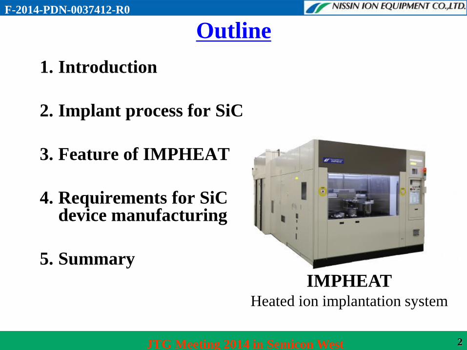
Outline
1. Introduction
2. Implant process for SiC
3. Feature of IMPHEAT
4. Requirements for SiC device manufacturing
5. Summary
IMPHEAT Heated ion implantation system

F-2014-PDN-0037412-R0
3 JTG Meeting 2014 in Semicon West
Growing market of power devices
Projected market growth of power devices
Bil
lio
n D
oll
ar
Source: Yano Research Institute Ltd. (2013)
Robotic suit kick off
in world cup 2014
Electric Vehicle
Bullet train
Air conditioner
Inverter for power
transmission
F-2014-PDN-0037412-R0
4 JTG Meeting 2014 in Semicon West
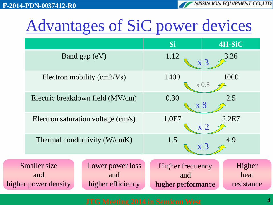
Advantages of SiC power devices Si 4H-SiC
Band gap (eV)
1.12 3.26
Electron mobility (cm2/Vs)
1400 1000
Electric breakdown field (MV/cm)
0.30 2.5
Electron saturation voltage (cm/s)
1.0E7 2.2E7
Thermal conductivity (W/cmK)
1.5 4.9
x 3
x 8
x 2
x 3
x 0.8
Smaller size
and
higher power density
Lower power loss
and
higher efficiency
Higher frequency
and
higher performance
Higher
heat
resistance

F-2014-PDN-0037412-R0
5 JTG Meeting 2014 in Semicon West
Ion implant process for SiC devices
☻Hard to re-crystalize SiC
☻Low dopant activation
☺Small diffusion of dopant
Heated ion implantation
Beam Energy
10 ~ 960keV
Dosage
5E11 ~ 1E16 /cm2
Dopant Al, P, B, N
Wafer Temperature Up to 500 oC
Wafer Size
100mm, 150mm
Channel implantation
F-2014-PDN-0037412-R0
6 JTG Meeting 2014 in Semicon West
Challenging with SiC substrate
• Crystallinity
• Dopant activation
• Measurement of substrate temperature
• Electro-static chucking of SiC
• Charging up with high resistivity substrate

F-2014-PDN-0037412-R0
7 JTG Meeting 2014 in Semicon West
NISSIN heated ion implant system
“IMPHEAT”
Based on EXCEED series
which are our field-proven
M/C tools
High Current Al ion beam
Heated implant capability up
to 500oC
Automatic wafer
transportation system for 6
or 4inch SiC wafer
The only tool for high-
temperature implant used
in mass production lines
for power devices
F-2014-PDN-0037412-R0
8 JTG Meeting 2014 in Semicon West
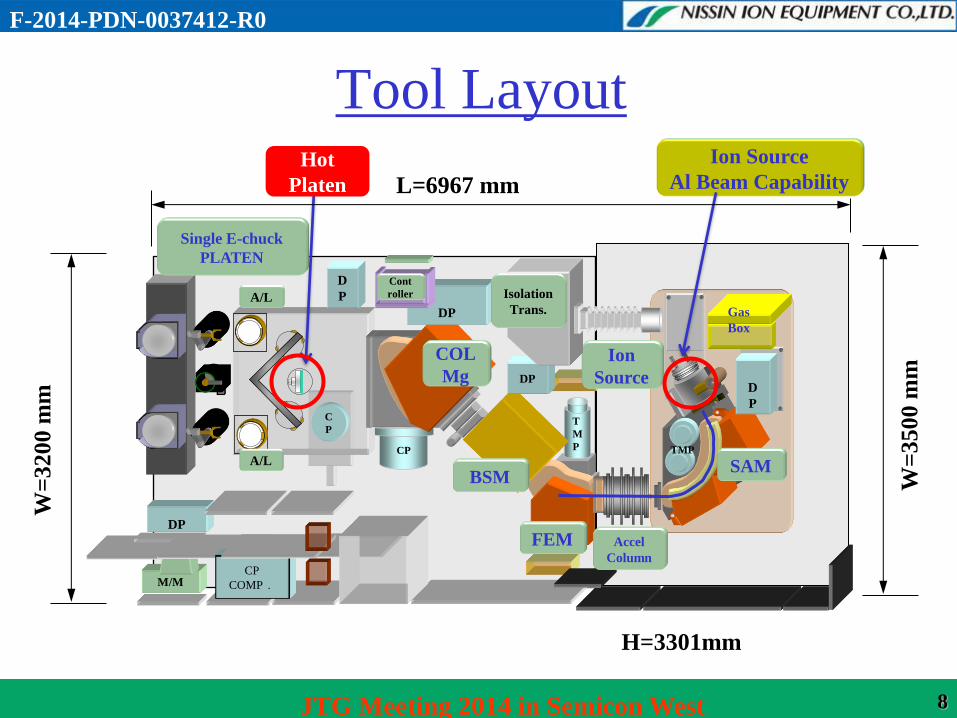
Tool Layout
CP
D
P
T
M
P
SAM
Ion
Source
FEM
Gas
Box
TMP
BSM
DP
C
P
COL
Mg
A/L
A/L
DP
Cont
roller
DP
M/M
D
P
Single E-chuck
PLATEN
Isolation
Trans.
CP
COMP.
Accel
Column
Ion Source
Al Beam Capability L=6967 mm
W=
3200 m
m
W=
3500 m
m
H=3301mm
Hot
Platen
F-2014-PDN-0037412-R0
9 JTG Meeting 2014 in Semicon West
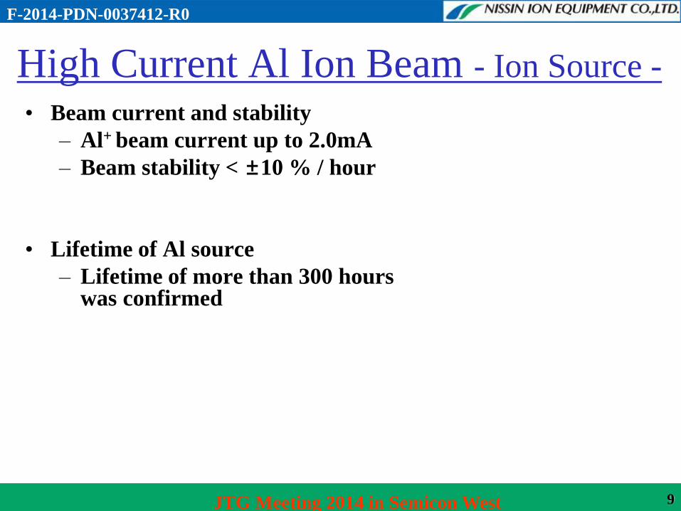
High Current Al Ion Beam - Ion Source -
9
• Beam current and stability
– Al+ beam current up to 2.0mA
– Beam stability < ±10 % / hour
• Lifetime of Al source
– Lifetime of more than 300 hours was confirmed
Al compound
(Al source)
F-2014-PDN-0037412-R0
10 JTG Meeting 2014 in Semicon West
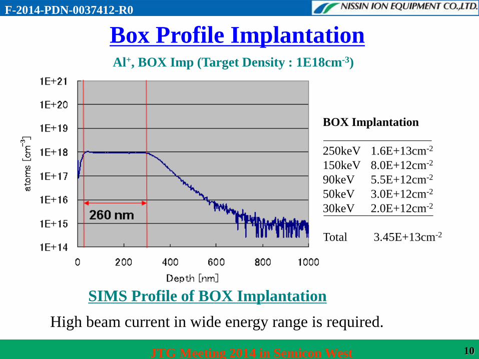
10
SIMS Profile of BOX Implantation
Al+, BOX Imp (Target Density : 1E18cm-3)
BOX Implantation
250keV 1.6E+13cm-2
150keV 8.0E+12cm-2
90keV 5.5E+12cm-2
50keV 3.0E+12cm-2
30keV 2.0E+12cm-2
Total 3.45E+13cm-2
Box Profile Implantation 3
High beam current in wide energy range is required.
F-2014-PDN-0037412-R0
11 JTG Meeting 2014 in Semicon West
11
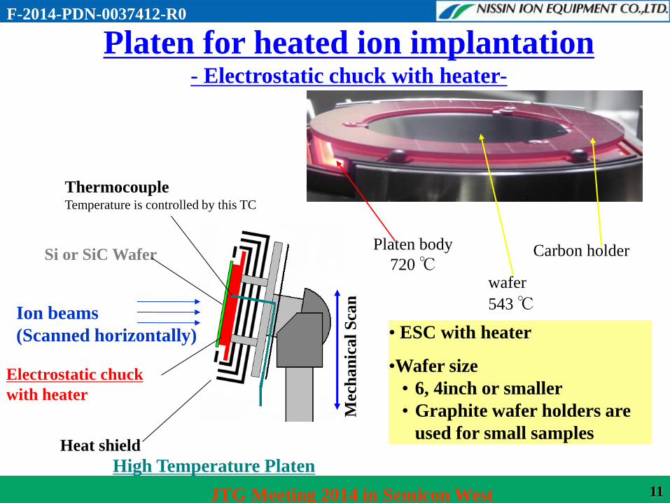
Ion beams
(Scanned horizontally)
Heat shield
Thermocouple Temperature is controlled by this TC
Si or SiC Wafer
Mech
an
ical
Sca
n
High Temperature Platen
Electrostatic chuck
with heater
Platen for heated ion implantation - Electrostatic chuck with heater-
wafer
Carbon holder
543 ℃
Platen body
720 ℃
• ESC with heater
•Wafer size
• 6, 4inch or smaller
• Graphite wafer holders are
used for small samples
F-2014-PDN-0037412-R0
12 JTG Meeting 2014 in Semicon West
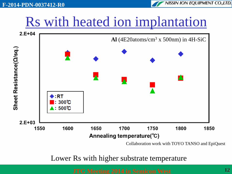
Rs with heated ion implantation
Lower Rs with higher substrate temperature
Collaboration work with TOYO TANSO and EpiQuest
Al (4E20atoms/cm3 x 500nm) in 4H-SiC

F-2014-PDN-0037412-R0
13 JTG Meeting 2014 in Semicon West
13
Pyrometer is adopted to measure the temperature of SiC 4H-N single crystal
wafer directly,
•4-7μm is the best wavelength to measure the temperature.
•CaF2 was selected as the material of the view port window.
The infrared rays characteristic of SiC The wafer temperature measurement system
Pyrometer
Monitoring system of wafer temperature
Pyrometer
Tra
nsm
issi
vit
y (
%)
Em
issi
vit
y (
%)
F-2014-PDN-0037412-R0
14 JTG Meeting 2014 in Semicon West
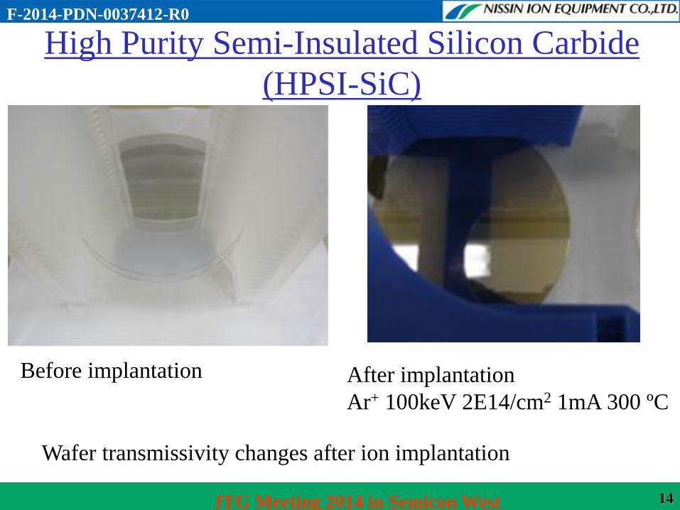
High Purity Semi-Insulated Silicon Carbide
(HPSI-SiC)
Before implantation After implantation
Ar+ 100keV 2E14/cm2 1mA 300 ºC
Wafer transmissivity changes after ion implantation

F-2014-PDN-0037412-R0
15 JTG Meeting 2014 in Semicon West
Transmissivity and emissivity changes after ion implantation in low
wavelength region.
Suitable wavelength for temperature observation changes depend on
the substrate.
Spectroscopic characteristics of HPSI-SiC
W. Zhao et al. IIT2014
F-2014-PDN-0037412-R0
16 JTG Meeting 2014 in Semicon West
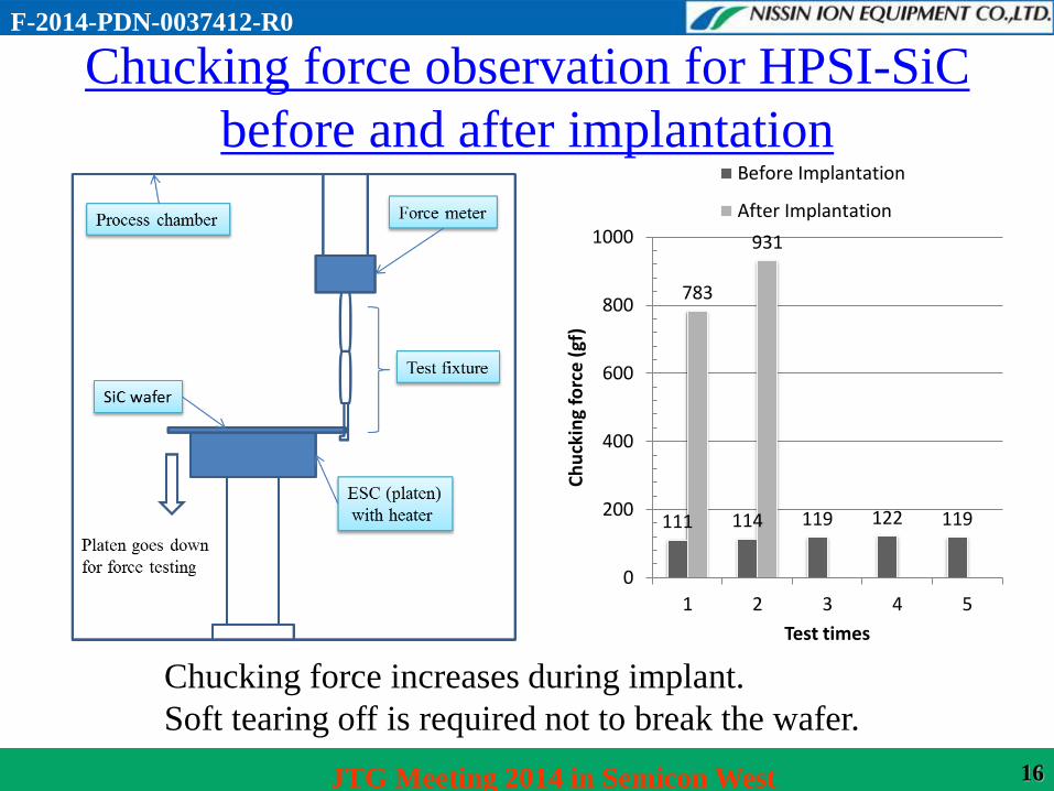
Chucking force observation for HPSI-SiC
before and after implantation
111 114 119 122 119
783
931
0
200
400
600
800
1000
1 2 3 4 5
Ch
uck
ing
forc
e (
gf)
Test times
Before Implantation
After Implantation
Chucking force increases during implant.
Soft tearing off is required not to break the wafer.

F-2014-PDN-0037412-R0
17 JTG Meeting 2014 in Semicon West
Temperature dependence of the Chucking force
ESC changes its electrical property as a function of temperature.
HT implant requires thermal insulation for heating, and RT implant requires thermal conductance for cooling.
Difficulty of implanting both at RT and HT in one configuration
Wide range of chucking force capability is required.
Our expertise for chucking force control and ESC design has
enabled both RT and HT implant in one configuration!
F-2014-PDN-0037412-R0
18 JTG Meeting 2014 in Semicon West
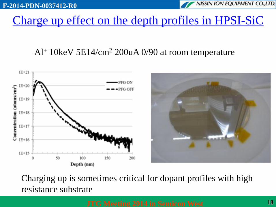
Charge up effect on the depth profiles in HPSI-SiC
Al+ 10keV 5E14/cm2 200uA 0/90 at room temperature
Charging up is sometimes critical for dopant profiles with high
resistance substrate

F-2014-PDN-0037412-R0
19 JTG Meeting 2014 in Semicon West
Plasma Flood Gun (PFG) of IMPHEAT®
Our powerful PFG helps to get designed dopant profiles supplying
low energy electrons to neutralize the charges on wafers.
F-2014-PDN-0037412-R0
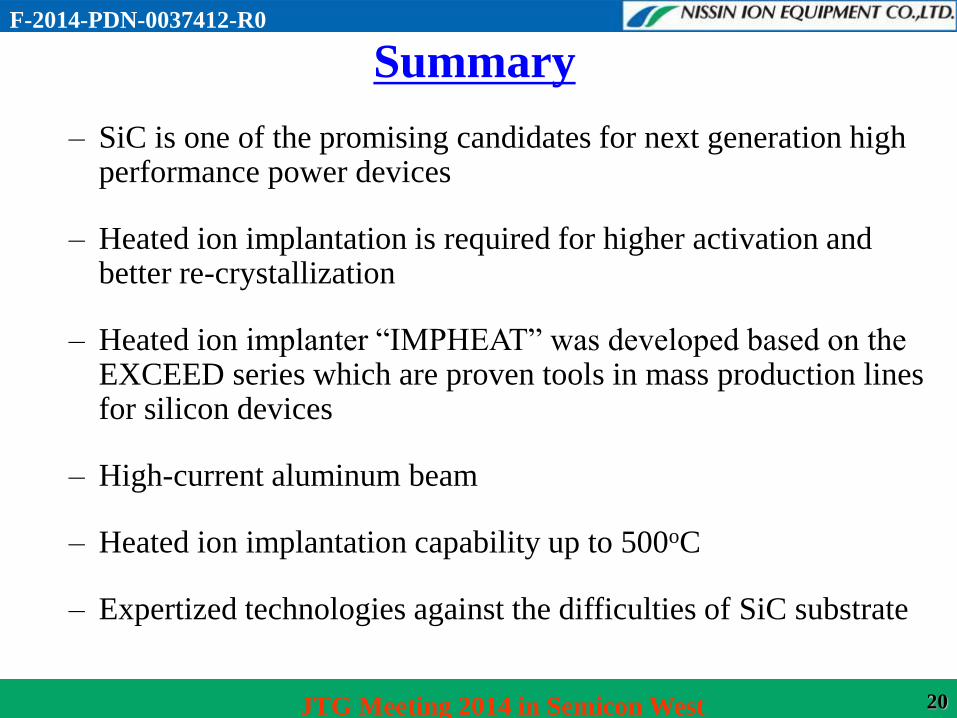
20 JTG Meeting 2014 in Semicon West
Summary
– SiC is one of the promising candidates for next generation high performance power devices
– Heated ion implantation is required for higher activation and better re-crystallization
– Heated ion implanter “IMPHEAT” was developed based on the EXCEED series which are proven tools in mass production lines for silicon devices
– High-current aluminum beam
– Heated ion implantation capability up to 500oC
– Expertized technologies against the difficulties of SiC substrate