here for production status of specific part numbers
TRANSCRIPT

General Description The MAX17301–MAX17303/MAX17311–MAX17313 is a 24μA IQ stand-alone pack-side fuel gauge IC with protec-tor and optional SHA-256 authentication for 1-cell lithium-ion/polymer batteries. The IC monitors the voltage, current, temperature, and state of the battery to provide against over/undervoltage, overcurrent, short-circuit, over/undertemperature and overcharge conditions protection using external high-side N-FETs, and provides charging prescription to ensure that the lithium-ion/polymer battery operates under safe condi-tions prolonging the life of the battery. To prevent battery pack cloning, the IC integrates SHA-256 authentication with a 160-bit secret key. Each IC incorporates a unique 64-bit ID. The fuel gauge uses ModelGauge m5 algorithm that com-bines the short-term accuracy and linearity of a coulomb counter with the long-term stability of a voltage-based fuel gauge to provide industry-leading fuel-gauge accuracy. The IC automatically compensates for cell aging, temper-ature, and discharge rate, and provides accurate state-of-charge (SOC) in milliampere-hours (mAh) or percentage (%) over a wide range of operating conditions. Dynamic power functionality provides the instantaneous maximum battery output power which can be delivered to the system without violating the minimum system input voltage. A Maxim 1-Wire® or 2-wire I2C interface provides access to data and control registers. The IC is available in a lead-free, 3mm x 3mm 14-pin TDFN and 1.7mm x 2.5mm 15-bump 0.5mm pitch WLP packages.
Applications Smartphones, Tablets, and 2-in-1 Laptops Smartwatches and Wearables Medical Devices, Health and Fitness Monitors Digital Still, Video, and Action Cameras Handheld Computers and Terminals Handheld Radios Home and Building Automation, Sensors Smart Batteries
Benefits and Features Battery Health + Programmable Safety/Protection
• Overvoltage (Temperature Dependent) • Overcharge Current • Over/Undertemperature • Ideal Diode Discharge During Charge Fault • Charging Prescriptions (JEITA) • Zero-Volt Charging Option • Undervoltage + SmartEmpty • Overdischarge/Short-Circuit
Nonvolatile Memory for Stand-Alone Operation • History Logging, User Data (122 Bytes)
Low Quiescent Current • FETs Enabled: 24µA Active, 18µA Hibernate • FETs Disabled: 7µA Ship, 0.5µA DeepShip,
0.1µA UV-Shutdown Pushbutton Wakeup—Eliminates System
Consumption Until Button Press ModelGauge m5 EZ Algorithm
• Percent, Capacity,Time-to-Empty/Full, Age • Cycle+™ Age Forecast
Dynamic Power—Estimates Power Capability Precision Measurement Without Calibration
• Current, Voltage, Power, Time, Cycles • Die Temperature/Thermistor
Ordering Information appears at end of datasheet.
Simple Fuel Gauge with Protector Circuit Diagram
REG
CSNCSP
SENSERESISTOR
PK+
MAX1730xMAX1730xMAXMAX1731x1731x
SDA/DQSCL/OD
ALRT/PIO HOSTµP
BATTERY PACK SYSTEM
PK-
BATT0.1µF
N N
0.1µFCP CHG DIS
OPTIONALNTC THERMISTOR
0.47µF
ZVC
PCKP
TH
PFAIL (MAX173x1 ONLY)
Secondary Protector
10Ω
1kΩ
(TDFN)EP
OPTIONAL
(WLP)GND
0.1µF
ModelGauge and Cycle+ are trademarks of Maxim Integrated Products, Inc. 1-Wire is a registered trademark of Maxim Integrated Products, Inc.
Click here for production status of specific part numbers.
MAX17301–MAX17303/MAX17311–MAX17313
1-Cell ModelGauge m5 EZ Fuel Gauge withProtector and SHA-256 Authentication
EVALUATION KIT AVAILABLE
19-100463; Rev 3; 5/19

TABLE OF CONTENTS General Description . . . . . . . . . . . . . . . . . . . . . . . . . . . . . . . . . . . . . . . . . . . . . . . . . . . . . . . . . . . . . . . . . . . . . . . . . . . . . . 1 Applications . . . . . . . . . . . . . . . . . . . . . . . . . . . . . . . . . . . . . . . . . . . . . . . . . . . . . . . . . . . . . . . . . . . . . . . . . . . . . . . . . . . . 1 Benefits and Features . . . . . . . . . . . . . . . . . . . . . . . . . . . . . . . . . . . . . . . . . . . . . . . . . . . . . . . . . . . . . . . . . . . . . . . . . . . . 1 Simple Fuel Gauge with Protector Circuit Diagram . . . . . . . . . . . . . . . . . . . . . . . . . . . . . . . . . . . . . . . . . . . . . . . . . . . . 1 Absolute Maximum Ratings . . . . . . . . . . . . . . . . . . . . . . . . . . . . . . . . . . . . . . . . . . . . . . . . . . . . . . . . . . . . . . . . . . . . . . . 16 Package Information . . . . . . . . . . . . . . . . . . . . . . . . . . . . . . . . . . . . . . . . . . . . . . . . . . . . . . . . . . . . . . . . . . . . . . . . . . . . 16
14 TDFN-EP . . . . . . . . . . . . . . . . . . . . . . . . . . . . . . . . . . . . . . . . . . . . . . . . . . . . . . . . . . . . . . . . . . . . . . . . . . . . . . . . 16 15 WLP . . . . . . . . . . . . . . . . . . . . . . . . . . . . . . . . . . . . . . . . . . . . . . . . . . . . . . . . . . . . . . . . . . . . . . . . . . . . . . . . . . . . 16
Electrical Characteristics . . . . . . . . . . . . . . . . . . . . . . . . . . . . . . . . . . . . . . . . . . . . . . . . . . . . . . . . . . . . . . . . . . . . . . . . 17 Typical Operating Characteristics . . . . . . . . . . . . . . . . . . . . . . . . . . . . . . . . . . . . . . . . . . . . . . . . . . . . . . . . . . . . . . . . . . 21 Pin Configurations . . . . . . . . . . . . . . . . . . . . . . . . . . . . . . . . . . . . . . . . . . . . . . . . . . . . . . . . . . . . . . . . . . . . . . . . . . . . . . 23
WLP . . . . . . . . . . . . . . . . . . . . . . . . . . . . . . . . . . . . . . . . . . . . . . . . . . . . . . . . . . . . . . . . . . . . . . . . . . . . . . . . . . . . . . 23 TDFN . . . . . . . . . . . . . . . . . . . . . . . . . . . . . . . . . . . . . . . . . . . . . . . . . . . . . . . . . . . . . . . . . . . . . . . . . . . . . . . . . . . . . 24
Pin Description . . . . . . . . . . . . . . . . . . . . . . . . . . . . . . . . . . . . . . . . . . . . . . . . . . . . . . . . . . . . . . . . . . . . . . . . . . . . . . . . 24 Functional Diagram . . . . . . . . . . . . . . . . . . . . . . . . . . . . . . . . . . . . . . . . . . . . . . . . . . . . . . . . . . . . . . . . . . . . . . . . . . . . . 26 Detailed Description . . . . . . . . . . . . . . . . . . . . . . . . . . . . . . . . . . . . . . . . . . . . . . . . . . . . . . . . . . . . . . . . . . . . . . . . . . . . 27
General Description . . . . . . . . . . . . . . . . . . . . . . . . . . . . . . . . . . . . . . . . . . . . . . . . . . . . . . . . . . . . . . . . . . . . . . . . . . 27 Protector . . . . . . . . . . . . . . . . . . . . . . . . . . . . . . . . . . . . . . . . . . . . . . . . . . . . . . . . . . . . . . . . . . . . . . . . . . . . . . . . . . . 28
Protector Thresholds . . . . . . . . . . . . . . . . . . . . . . . . . . . . . . . . . . . . . . . . . . . . . . . . . . . . . . . . . . . . . . . . . . . . . . . 33 Voltage Thresholds . . . . . . . . . . . . . . . . . . . . . . . . . . . . . . . . . . . . . . . . . . . . . . . . . . . . . . . . . . . . . . . . . . . . . . 33 Ideal Diode Behavior . . . . . . . . . . . . . . . . . . . . . . . . . . . . . . . . . . . . . . . . . . . . . . . . . . . . . . . . . . . . . . . . . . . . . 34 Current Thresholds . . . . . . . . . . . . . . . . . . . . . . . . . . . . . . . . . . . . . . . . . . . . . . . . . . . . . . . . . . . . . . . . . . . . . . 35
Overcurrent Protection . . . . . . . . . . . . . . . . . . . . . . . . . . . . . . . . . . . . . . . . . . . . . . . . . . . . . . . . . . . . . . . . . 36 Fast Overcurrent Comparators . . . . . . . . . . . . . . . . . . . . . . . . . . . . . . . . . . . . . . . . . . . . . . . . . . . . . . . . . 37
Overcurrent Comparator Diagram . . . . . . . . . . . . . . . . . . . . . . . . . . . . . . . . . . . . . . . . . . . . . . . . . . . . 37 Slow Overcurrent Protection . . . . . . . . . . . . . . . . . . . . . . . . . . . . . . . . . . . . . . . . . . . . . . . . . . . . . . . . . . . 37
Temperature Thresholds . . . . . . . . . . . . . . . . . . . . . . . . . . . . . . . . . . . . . . . . . . . . . . . . . . . . . . . . . . . . . . . . . . 37 Other Thresholds . . . . . . . . . . . . . . . . . . . . . . . . . . . . . . . . . . . . . . . . . . . . . . . . . . . . . . . . . . . . . . . . . . . . . . . . 38 Disabling FETs by Pin-Control or I2C Command . . . . . . . . . . . . . . . . . . . . . . . . . . . . . . . . . . . . . . . . . . . . . . . . 38 Charging Prescription . . . . . . . . . . . . . . . . . . . . . . . . . . . . . . . . . . . . . . . . . . . . . . . . . . . . . . . . . . . . . . . . . . . . 38
Step Charging . . . . . . . . . . . . . . . . . . . . . . . . . . . . . . . . . . . . . . . . . . . . . . . . . . . . . . . . . . . . . . . . . . . . . . . . 39 Zero-Volt Charging . . . . . . . . . . . . . . . . . . . . . . . . . . . . . . . . . . . . . . . . . . . . . . . . . . . . . . . . . . . . . . . . . . . . . . . . . 39
ModelGauge m5 Algorithm . . . . . . . . . . . . . . . . . . . . . . . . . . . . . . . . . . . . . . . . . . . . . . . . . . . . . . . . . . . . . . . . . . . . . 41 Wakeup/Shutdown . . . . . . . . . . . . . . . . . . . . . . . . . . . . . . . . . . . . . . . . . . . . . . . . . . . . . . . . . . . . . . . . . . . . . . . . . . . 43
Modes of Operation . . . . . . . . . . . . . . . . . . . . . . . . . . . . . . . . . . . . . . . . . . . . . . . . . . . . . . . . . . . . . . . . . . . . . . . . 43 Power Mode Transition State Diagram . . . . . . . . . . . . . . . . . . . . . . . . . . . . . . . . . . . . . . . . . . . . . . . . . . . . . . . . . 45 Pushbutton Wakeup . . . . . . . . . . . . . . . . . . . . . . . . . . . . . . . . . . . . . . . . . . . . . . . . . . . . . . . . . . . . . . . . . . . . . . . . 46
MAX17301–MAX17303/MAX17311–MAX17313
1-Cell ModelGauge m5 EZ Fuel Gauge withProtector and SHA-256 Authentication
www.maximintegrated.com Maxim Integrated | 2

TABLE OF CONTENTS (CONTINUED) Register Description Conventions . . . . . . . . . . . . . . . . . . . . . . . . . . . . . . . . . . . . . . . . . . . . . . . . . . . . . . . . . . . . . . . . 46
Standard Register Formats . . . . . . . . . . . . . . . . . . . . . . . . . . . . . . . . . . . . . . . . . . . . . . . . . . . . . . . . . . . . . . . . . . 46 Device Reset . . . . . . . . . . . . . . . . . . . . . . . . . . . . . . . . . . . . . . . . . . . . . . . . . . . . . . . . . . . . . . . . . . . . . . . . . . . . . 46 Nonvolatile Backup and Initial Value . . . . . . . . . . . . . . . . . . . . . . . . . . . . . . . . . . . . . . . . . . . . . . . . . . . . . . . . . . . 46 Register Naming Conventions . . . . . . . . . . . . . . . . . . . . . . . . . . . . . . . . . . . . . . . . . . . . . . . . . . . . . . . . . . . . . . . . 47
Protection Registers . . . . . . . . . . . . . . . . . . . . . . . . . . . . . . . . . . . . . . . . . . . . . . . . . . . . . . . . . . . . . . . . . . . . . . . . . . 47 Voltage Protection Registers . . . . . . . . . . . . . . . . . . . . . . . . . . . . . . . . . . . . . . . . . . . . . . . . . . . . . . . . . . . . . . . . . 47
nVPrtTh1 Register (1D0h) . . . . . . . . . . . . . . . . . . . . . . . . . . . . . . . . . . . . . . . . . . . . . . . . . . . . . . . . . . . . . . . . . 47 nVPrtTh2 Register (1D4h) . . . . . . . . . . . . . . . . . . . . . . . . . . . . . . . . . . . . . . . . . . . . . . . . . . . . . . . . . . . . . . . . . 47 nJEITAV Register (1D9h) . . . . . . . . . . . . . . . . . . . . . . . . . . . . . . . . . . . . . . . . . . . . . . . . . . . . . . . . . . . . . . . . . 47 nJEITACfg Register (1DAh) . . . . . . . . . . . . . . . . . . . . . . . . . . . . . . . . . . . . . . . . . . . . . . . . . . . . . . . . . . . . . . . . 48
Current Protection Registers . . . . . . . . . . . . . . . . . . . . . . . . . . . . . . . . . . . . . . . . . . . . . . . . . . . . . . . . . . . . . . . . . 48 nODSCTh Register (1DDh) . . . . . . . . . . . . . . . . . . . . . . . . . . . . . . . . . . . . . . . . . . . . . . . . . . . . . . . . . . . . . . . . 49 nODSCCfg Register (1DEh) . . . . . . . . . . . . . . . . . . . . . . . . . . . . . . . . . . . . . . . . . . . . . . . . . . . . . . . . . . . . . . . 49 nIPrtTh1 Register (1D3h)—Overcurrent Protection Thresholds . . . . . . . . . . . . . . . . . . . . . . . . . . . . . . . . . . . . 50 nJEITAC Register (1D8h) . . . . . . . . . . . . . . . . . . . . . . . . . . . . . . . . . . . . . . . . . . . . . . . . . . . . . . . . . . . . . . . . . 50
Temperature Protection Registers . . . . . . . . . . . . . . . . . . . . . . . . . . . . . . . . . . . . . . . . . . . . . . . . . . . . . . . . . . . . . 51 nTPrtTh1 Register (1D1h) . . . . . . . . . . . . . . . . . . . . . . . . . . . . . . . . . . . . . . . . . . . . . . . . . . . . . . . . . . . . . . . . . 51 nTPrtTh2 Register (1D5h) . . . . . . . . . . . . . . . . . . . . . . . . . . . . . . . . . . . . . . . . . . . . . . . . . . . . . . . . . . . . . . . . . 51 nTPrtTh3 Register (1D2h) (beyond JEITA) . . . . . . . . . . . . . . . . . . . . . . . . . . . . . . . . . . . . . . . . . . . . . . . . . . . . 52
Fault Timer Registers . . . . . . . . . . . . . . . . . . . . . . . . . . . . . . . . . . . . . . . . . . . . . . . . . . . . . . . . . . . . . . . . . . . . . . . 52 nDelayCfg Register (1DCh) . . . . . . . . . . . . . . . . . . . . . . . . . . . . . . . . . . . . . . . . . . . . . . . . . . . . . . . . . . . . . . . . 52
Status/Configuration Protection Registers . . . . . . . . . . . . . . . . . . . . . . . . . . . . . . . . . . . . . . . . . . . . . . . . . . . . . . . 54 nProtCfg Register (1D7h) . . . . . . . . . . . . . . . . . . . . . . . . . . . . . . . . . . . . . . . . . . . . . . . . . . . . . . . . . . . . . . . . . 54 nBattStatus Register (1A8h) . . . . . . . . . . . . . . . . . . . . . . . . . . . . . . . . . . . . . . . . . . . . . . . . . . . . . . . . . . . . . . . 55 ProtStatus Register (0D9h) . . . . . . . . . . . . . . . . . . . . . . . . . . . . . . . . . . . . . . . . . . . . . . . . . . . . . . . . . . . . . . . . 55 HConfig2 Register (1F5h) . . . . . . . . . . . . . . . . . . . . . . . . . . . . . . . . . . . . . . . . . . . . . . . . . . . . . . . . . . . . . . . . . 56
Other Protection Registers . . . . . . . . . . . . . . . . . . . . . . . . . . . . . . . . . . . . . . . . . . . . . . . . . . . . . . . . . . . . . . . . . . . 57 nProtMiscTh Register (1D6h) . . . . . . . . . . . . . . . . . . . . . . . . . . . . . . . . . . . . . . . . . . . . . . . . . . . . . . . . . . . . . . 57
Charging Prescription Registers . . . . . . . . . . . . . . . . . . . . . . . . . . . . . . . . . . . . . . . . . . . . . . . . . . . . . . . . . . . . . . . 57 ChargingCurrent Register (028h) . . . . . . . . . . . . . . . . . . . . . . . . . . . . . . . . . . . . . . . . . . . . . . . . . . . . . . . . . . . . 57 ChargingVoltage Register (02Ah) . . . . . . . . . . . . . . . . . . . . . . . . . . . . . . . . . . . . . . . . . . . . . . . . . . . . . . . . . . . 57 nStepChg Register (1DBh) . . . . . . . . . . . . . . . . . . . . . . . . . . . . . . . . . . . . . . . . . . . . . . . . . . . . . . . . . . . . . . . . 57
ModelGauge m5 Algorithm . . . . . . . . . . . . . . . . . . . . . . . . . . . . . . . . . . . . . . . . . . . . . . . . . . . . . . . . . . . . . . . . . . . . . 58 ModelGauge m5 Registers . . . . . . . . . . . . . . . . . . . . . . . . . . . . . . . . . . . . . . . . . . . . . . . . . . . . . . . . . . . . . . . . . . . 58 ModelGauge m5 Algorithm Output Registers . . . . . . . . . . . . . . . . . . . . . . . . . . . . . . . . . . . . . . . . . . . . . . . . . . . . . 59
RepCap Register (005h) . . . . . . . . . . . . . . . . . . . . . . . . . . . . . . . . . . . . . . . . . . . . . . . . . . . . . . . . . . . . . . . . . . 59 RepSOC Register (006h) . . . . . . . . . . . . . . . . . . . . . . . . . . . . . . . . . . . . . . . . . . . . . . . . . . . . . . . . . . . . . . . . . . 59
MAX17301–MAX17303/MAX17311–MAX17313
1-Cell ModelGauge m5 EZ Fuel Gauge withProtector and SHA-256 Authentication
www.maximintegrated.com Maxim Integrated | 3

TABLE OF CONTENTS (CONTINUED) FullCapRep Register (010h) . . . . . . . . . . . . . . . . . . . . . . . . . . . . . . . . . . . . . . . . . . . . . . . . . . . . . . . . . . . . . . . 59 TTE Register (011h) . . . . . . . . . . . . . . . . . . . . . . . . . . . . . . . . . . . . . . . . . . . . . . . . . . . . . . . . . . . . . . . . . . . . . 59 TTF Register (020h) . . . . . . . . . . . . . . . . . . . . . . . . . . . . . . . . . . . . . . . . . . . . . . . . . . . . . . . . . . . . . . . . . . . . . . 59 Age Register (007h) . . . . . . . . . . . . . . . . . . . . . . . . . . . . . . . . . . . . . . . . . . . . . . . . . . . . . . . . . . . . . . . . . . . . . . 59 Cycles Register (017h) and nCycles (1A4h) . . . . . . . . . . . . . . . . . . . . . . . . . . . . . . . . . . . . . . . . . . . . . . . . . . . 60 TimerH Register (0BEh) . . . . . . . . . . . . . . . . . . . . . . . . . . . . . . . . . . . . . . . . . . . . . . . . . . . . . . . . . . . . . . . . . . 60 FullCap Register (010h) . . . . . . . . . . . . . . . . . . . . . . . . . . . . . . . . . . . . . . . . . . . . . . . . . . . . . . . . . . . . . . . . . . . 60 nFullCapNom Register (1A5h) . . . . . . . . . . . . . . . . . . . . . . . . . . . . . . . . . . . . . . . . . . . . . . . . . . . . . . . . . . . . . . 61 RCell Register (014h) . . . . . . . . . . . . . . . . . . . . . . . . . . . . . . . . . . . . . . . . . . . . . . . . . . . . . . . . . . . . . . . . . . . . 61 VRipple Register (0B2h) . . . . . . . . . . . . . . . . . . . . . . . . . . . . . . . . . . . . . . . . . . . . . . . . . . . . . . . . . . . . . . . . . . 61 nVoltTemp Register (1AAh) . . . . . . . . . . . . . . . . . . . . . . . . . . . . . . . . . . . . . . . . . . . . . . . . . . . . . . . . . . . . . . . . 61 SOCHold Register (0D0h) . . . . . . . . . . . . . . . . . . . . . . . . . . . . . . . . . . . . . . . . . . . . . . . . . . . . . . . . . . . . . . . . . 61
ModelGauge m5 EZ Performance . . . . . . . . . . . . . . . . . . . . . . . . . . . . . . . . . . . . . . . . . . . . . . . . . . . . . . . . . . . . . 62 OCV Estimation and Coulomb Count Mixing . . . . . . . . . . . . . . . . . . . . . . . . . . . . . . . . . . . . . . . . . . . . . . . . . . . . . 62 Empty Compensation . . . . . . . . . . . . . . . . . . . . . . . . . . . . . . . . . . . . . . . . . . . . . . . . . . . . . . . . . . . . . . . . . . . . . . . 64 End-of-Charge Detection . . . . . . . . . . . . . . . . . . . . . . . . . . . . . . . . . . . . . . . . . . . . . . . . . . . . . . . . . . . . . . . . . . . . 65 Fuel Gauge Learning . . . . . . . . . . . . . . . . . . . . . . . . . . . . . . . . . . . . . . . . . . . . . . . . . . . . . . . . . . . . . . . . . . . . . . . 67 Converge-To-Empty . . . . . . . . . . . . . . . . . . . . . . . . . . . . . . . . . . . . . . . . . . . . . . . . . . . . . . . . . . . . . . . . . . . . . . . . 68 Determining Fuel-Gauge Accuracy . . . . . . . . . . . . . . . . . . . . . . . . . . . . . . . . . . . . . . . . . . . . . . . . . . . . . . . . . . . . 69 Initial Accuracy . . . . . . . . . . . . . . . . . . . . . . . . . . . . . . . . . . . . . . . . . . . . . . . . . . . . . . . . . . . . . . . . . . . . . . . . . . . . 69 Cycle+ Age Forecasting . . . . . . . . . . . . . . . . . . . . . . . . . . . . . . . . . . . . . . . . . . . . . . . . . . . . . . . . . . . . . . . . . . . . . 70
nAgeFcCfg Register (1E2h) . . . . . . . . . . . . . . . . . . . . . . . . . . . . . . . . . . . . . . . . . . . . . . . . . . . . . . . . . . . . . . . . 70 AgeForecast Register (0B9h) . . . . . . . . . . . . . . . . . . . . . . . . . . . . . . . . . . . . . . . . . . . . . . . . . . . . . . . . . . . . . . 71 Age Forecasting Requirements . . . . . . . . . . . . . . . . . . . . . . . . . . . . . . . . . . . . . . . . . . . . . . . . . . . . . . . . . . . . . 71 Enabling Age Forecasting . . . . . . . . . . . . . . . . . . . . . . . . . . . . . . . . . . . . . . . . . . . . . . . . . . . . . . . . . . . . . . . . . 71
Battery Life Logging . . . . . . . . . . . . . . . . . . . . . . . . . . . . . . . . . . . . . . . . . . . . . . . . . . . . . . . . . . . . . . . . . . . . . . . . 72 Life Logging Data Example . . . . . . . . . . . . . . . . . . . . . . . . . . . . . . . . . . . . . . . . . . . . . . . . . . . . . . . . . . . . . . . . 72 Determining Number of Valid Logging Entries . . . . . . . . . . . . . . . . . . . . . . . . . . . . . . . . . . . . . . . . . . . . . . . . . . 73 Reading History Data . . . . . . . . . . . . . . . . . . . . . . . . . . . . . . . . . . . . . . . . . . . . . . . . . . . . . . . . . . . . . . . . . . . . . 76 History Data Reading Example . . . . . . . . . . . . . . . . . . . . . . . . . . . . . . . . . . . . . . . . . . . . . . . . . . . . . . . . . . . . . 76
ModelGauge m5 Algorithm Input Registers . . . . . . . . . . . . . . . . . . . . . . . . . . . . . . . . . . . . . . . . . . . . . . . . . . . . . . 76 nXTable0 (180h) to nXTable11 (18Bh) Registers . . . . . . . . . . . . . . . . . . . . . . . . . . . . . . . . . . . . . . . . . . . . . . . 76 nOCVTable0 (190h) to nOCVTable11 (19Bh) Registers . . . . . . . . . . . . . . . . . . . . . . . . . . . . . . . . . . . . . . . . . . 77 nQRTable00 (1A0h) to nQRTable30 (1A3h) Registers . . . . . . . . . . . . . . . . . . . . . . . . . . . . . . . . . . . . . . . . . . . 77 nFullSOCThr Register (1C6h) . . . . . . . . . . . . . . . . . . . . . . . . . . . . . . . . . . . . . . . . . . . . . . . . . . . . . . . . . . . . . . 77 nVEmpty Register (19Eh) . . . . . . . . . . . . . . . . . . . . . . . . . . . . . . . . . . . . . . . . . . . . . . . . . . . . . . . . . . . . . . . . . 77 nDesignCap Register(1B3h) . . . . . . . . . . . . . . . . . . . . . . . . . . . . . . . . . . . . . . . . . . . . . . . . . . . . . . . . . . . . . . . 78 nRFast Register (1E5h) . . . . . . . . . . . . . . . . . . . . . . . . . . . . . . . . . . . . . . . . . . . . . . . . . . . . . . . . . . . . . . . . . . . 78
MAX17301–MAX17303/MAX17311–MAX17313
1-Cell ModelGauge m5 EZ Fuel Gauge withProtector and SHA-256 Authentication
www.maximintegrated.com Maxim Integrated | 4

TABLE OF CONTENTS (CONTINUED) nIChgTerm Register (19Ch) . . . . . . . . . . . . . . . . . . . . . . . . . . . . . . . . . . . . . . . . . . . . . . . . . . . . . . . . . . . . . . . . 78 nRComp0 Register (1A6h) . . . . . . . . . . . . . . . . . . . . . . . . . . . . . . . . . . . . . . . . . . . . . . . . . . . . . . . . . . . . . . . . . 78 nTempCo Register (1A7h) . . . . . . . . . . . . . . . . . . . . . . . . . . . . . . . . . . . . . . . . . . . . . . . . . . . . . . . . . . . . . . . . . 79 nIAvgEmpty Register (1A8h) . . . . . . . . . . . . . . . . . . . . . . . . . . . . . . . . . . . . . . . . . . . . . . . . . . . . . . . . . . . . . . . 79
ModelGauge m5 Algorithm Configuration Registers . . . . . . . . . . . . . . . . . . . . . . . . . . . . . . . . . . . . . . . . . . . . . . . 79 nFilterCfg Register (19Dh) . . . . . . . . . . . . . . . . . . . . . . . . . . . . . . . . . . . . . . . . . . . . . . . . . . . . . . . . . . . . . . . . . 79 nRelaxCfg Register (1B6h) . . . . . . . . . . . . . . . . . . . . . . . . . . . . . . . . . . . . . . . . . . . . . . . . . . . . . . . . . . . . . . . . 80 nTTFCfg Register (1C7h)/CV_MixCap (0B6h) and CV_HalfTime (0B7h) Registers . . . . . . . . . . . . . . . . . . . . . 81 nConvgCfg Register (1B7h) . . . . . . . . . . . . . . . . . . . . . . . . . . . . . . . . . . . . . . . . . . . . . . . . . . . . . . . . . . . . . . . . 81 nRippleCfg Register (1B1h) . . . . . . . . . . . . . . . . . . . . . . . . . . . . . . . . . . . . . . . . . . . . . . . . . . . . . . . . . . . . . . . . 82
ModelGauge m5 Algorithm Additional Registers . . . . . . . . . . . . . . . . . . . . . . . . . . . . . . . . . . . . . . . . . . . . . . . . . . 82 Timer Register (03Eh) . . . . . . . . . . . . . . . . . . . . . . . . . . . . . . . . . . . . . . . . . . . . . . . . . . . . . . . . . . . . . . . . . . . . 82 dQAcc Register (045h) . . . . . . . . . . . . . . . . . . . . . . . . . . . . . . . . . . . . . . . . . . . . . . . . . . . . . . . . . . . . . . . . . . . 83 dPAcc Register (046h) . . . . . . . . . . . . . . . . . . . . . . . . . . . . . . . . . . . . . . . . . . . . . . . . . . . . . . . . . . . . . . . . . . . . 83 QResidual Register (00Ch) . . . . . . . . . . . . . . . . . . . . . . . . . . . . . . . . . . . . . . . . . . . . . . . . . . . . . . . . . . . . . . . . 83 VFSOC Register (0FFh) . . . . . . . . . . . . . . . . . . . . . . . . . . . . . . . . . . . . . . . . . . . . . . . . . . . . . . . . . . . . . . . . . . 83 VFOCV Register (0FBh) . . . . . . . . . . . . . . . . . . . . . . . . . . . . . . . . . . . . . . . . . . . . . . . . . . . . . . . . . . . . . . . . . . 83 QH Register (4Dh) . . . . . . . . . . . . . . . . . . . . . . . . . . . . . . . . . . . . . . . . . . . . . . . . . . . . . . . . . . . . . . . . . . . . . . . 83 AvCap Register (01Fh) . . . . . . . . . . . . . . . . . . . . . . . . . . . . . . . . . . . . . . . . . . . . . . . . . . . . . . . . . . . . . . . . . . . 83 AvSOC Register (00Eh) . . . . . . . . . . . . . . . . . . . . . . . . . . . . . . . . . . . . . . . . . . . . . . . . . . . . . . . . . . . . . . . . . . . 84 MixSOC Register (00Dh) . . . . . . . . . . . . . . . . . . . . . . . . . . . . . . . . . . . . . . . . . . . . . . . . . . . . . . . . . . . . . . . . . . 84 MixCap Register (02Bh) . . . . . . . . . . . . . . . . . . . . . . . . . . . . . . . . . . . . . . . . . . . . . . . . . . . . . . . . . . . . . . . . . . . 84 VFRemCap Register (04Ah) . . . . . . . . . . . . . . . . . . . . . . . . . . . . . . . . . . . . . . . . . . . . . . . . . . . . . . . . . . . . . . . 84 FStat Register (03Dh) . . . . . . . . . . . . . . . . . . . . . . . . . . . . . . . . . . . . . . . . . . . . . . . . . . . . . . . . . . . . . . . . . . . . 84
Memory . . . . . . . . . . . . . . . . . . . . . . . . . . . . . . . . . . . . . . . . . . . . . . . . . . . . . . . . . . . . . . . . . . . . . . . . . . . . . . . . . . . . 85 ModelGauge m5 Memory Space . . . . . . . . . . . . . . . . . . . . . . . . . . . . . . . . . . . . . . . . . . . . . . . . . . . . . . . . . . . . . . 86 Nonvolatile Memory . . . . . . . . . . . . . . . . . . . . . . . . . . . . . . . . . . . . . . . . . . . . . . . . . . . . . . . . . . . . . . . . . . . . . . . . 87
Nonvolatile Memory Map . . . . . . . . . . . . . . . . . . . . . . . . . . . . . . . . . . . . . . . . . . . . . . . . . . . . . . . . . . . . . . . . . . 87 100 Record Life Logging . . . . . . . . . . . . . . . . . . . . . . . . . . . . . . . . . . . . . . . . . . . . . . . . . . . . . . . . . . . . . . . . . . 87 nNVCfg0 Register (1B8h) . . . . . . . . . . . . . . . . . . . . . . . . . . . . . . . . . . . . . . . . . . . . . . . . . . . . . . . . . . . . . . . . . 89 nNVCfg1 Register (1B9h) . . . . . . . . . . . . . . . . . . . . . . . . . . . . . . . . . . . . . . . . . . . . . . . . . . . . . . . . . . . . . . . . . 91 nNVCfg2 Register (1BAh) . . . . . . . . . . . . . . . . . . . . . . . . . . . . . . . . . . . . . . . . . . . . . . . . . . . . . . . . . . . . . . . . . 92 Enabling and Freeing Nonvolatile vs. Defaults . . . . . . . . . . . . . . . . . . . . . . . . . . . . . . . . . . . . . . . . . . . . . . . . . 93 Shadow RAM . . . . . . . . . . . . . . . . . . . . . . . . . . . . . . . . . . . . . . . . . . . . . . . . . . . . . . . . . . . . . . . . . . . . . . . . . . . 99
Shadow RAM and Nonvolatile Memory Relationship . . . . . . . . . . . . . . . . . . . . . . . . . . . . . . . . . . . . . . . . . 100 Nonvolatile Memory Commands . . . . . . . . . . . . . . . . . . . . . . . . . . . . . . . . . . . . . . . . . . . . . . . . . . . . . . . . . . . 100
COPY NV BLOCK [E904h] . . . . . . . . . . . . . . . . . . . . . . . . . . . . . . . . . . . . . . . . . . . . . . . . . . . . . . . . . . . . . 100 NV RECALL [E001h] . . . . . . . . . . . . . . . . . . . . . . . . . . . . . . . . . . . . . . . . . . . . . . . . . . . . . . . . . . . . . . . . . . 100
MAX17301–MAX17303/MAX17311–MAX17313
1-Cell ModelGauge m5 EZ Fuel Gauge withProtector and SHA-256 Authentication
www.maximintegrated.com Maxim Integrated | 5

TABLE OF CONTENTS (CONTINUED) HISTORY RECALL [E2XXh] . . . . . . . . . . . . . . . . . . . . . . . . . . . . . . . . . . . . . . . . . . . . . . . . . . . . . . . . . . . . 100
Nonvolatile Block Programming . . . . . . . . . . . . . . . . . . . . . . . . . . . . . . . . . . . . . . . . . . . . . . . . . . . . . . . . . . . . 101 Determining Number of Remaining Updates . . . . . . . . . . . . . . . . . . . . . . . . . . . . . . . . . . . . . . . . . . . . . . . . . . 101 nLearnCfg Register (19Fh) . . . . . . . . . . . . . . . . . . . . . . . . . . . . . . . . . . . . . . . . . . . . . . . . . . . . . . . . . . . . . . . 102 nMiscCfg Register (1B2h) . . . . . . . . . . . . . . . . . . . . . . . . . . . . . . . . . . . . . . . . . . . . . . . . . . . . . . . . . . . . . . . . 103 nConfig Register (1B0h) . . . . . . . . . . . . . . . . . . . . . . . . . . . . . . . . . . . . . . . . . . . . . . . . . . . . . . . . . . . . . . . . . 103 nPackCfg Register(1B5h) . . . . . . . . . . . . . . . . . . . . . . . . . . . . . . . . . . . . . . . . . . . . . . . . . . . . . . . . . . . . . . . . 105 nDesignVoltage Register (1E3h) . . . . . . . . . . . . . . . . . . . . . . . . . . . . . . . . . . . . . . . . . . . . . . . . . . . . . . . . . . . 105
Memory Locks . . . . . . . . . . . . . . . . . . . . . . . . . . . . . . . . . . . . . . . . . . . . . . . . . . . . . . . . . . . . . . . . . . . . . . . . . . . 105 NV LOCK [6AXXh] . . . . . . . . . . . . . . . . . . . . . . . . . . . . . . . . . . . . . . . . . . . . . . . . . . . . . . . . . . . . . . . . . . . . . . 106 Locking Memory Blocks . . . . . . . . . . . . . . . . . . . . . . . . . . . . . . . . . . . . . . . . . . . . . . . . . . . . . . . . . . . . . . . . . . 106 Reading Lock State . . . . . . . . . . . . . . . . . . . . . . . . . . . . . . . . . . . . . . . . . . . . . . . . . . . . . . . . . . . . . . . . . . . . . 106
Analog Measurements . . . . . . . . . . . . . . . . . . . . . . . . . . . . . . . . . . . . . . . . . . . . . . . . . . . . . . . . . . . . . . . . . . . . . . . 107 Voltage Measurement . . . . . . . . . . . . . . . . . . . . . . . . . . . . . . . . . . . . . . . . . . . . . . . . . . . . . . . . . . . . . . . . . . . . . 107
VCell Register (01Ah) . . . . . . . . . . . . . . . . . . . . . . . . . . . . . . . . . . . . . . . . . . . . . . . . . . . . . . . . . . . . . . . . . . . 107 AvgVCell Register (019h) . . . . . . . . . . . . . . . . . . . . . . . . . . . . . . . . . . . . . . . . . . . . . . . . . . . . . . . . . . . . . . . . 107 MaxMinVolt Register (0008h) . . . . . . . . . . . . . . . . . . . . . . . . . . . . . . . . . . . . . . . . . . . . . . . . . . . . . . . . . . . . . 107 MinVolt Register (0ADh) . . . . . . . . . . . . . . . . . . . . . . . . . . . . . . . . . . . . . . . . . . . . . . . . . . . . . . . . . . . . . . . . . 108 Cell1 Register (0D8h) . . . . . . . . . . . . . . . . . . . . . . . . . . . . . . . . . . . . . . . . . . . . . . . . . . . . . . . . . . . . . . . . . . . 108 AvgCell1 Register (0D4h) . . . . . . . . . . . . . . . . . . . . . . . . . . . . . . . . . . . . . . . . . . . . . . . . . . . . . . . . . . . . . . . . 108 Batt Register (0D7h) . . . . . . . . . . . . . . . . . . . . . . . . . . . . . . . . . . . . . . . . . . . . . . . . . . . . . . . . . . . . . . . . . . . . 108
Current Measurement . . . . . . . . . . . . . . . . . . . . . . . . . . . . . . . . . . . . . . . . . . . . . . . . . . . . . . . . . . . . . . . . . . . . . 108 Current Measurement Timing . . . . . . . . . . . . . . . . . . . . . . . . . . . . . . . . . . . . . . . . . . . . . . . . . . . . . . . . . . . . . 109 Current Register (01Ch) . . . . . . . . . . . . . . . . . . . . . . . . . . . . . . . . . . . . . . . . . . . . . . . . . . . . . . . . . . . . . . . . . . 109 AvgCurrent Register (01Dh) . . . . . . . . . . . . . . . . . . . . . . . . . . . . . . . . . . . . . . . . . . . . . . . . . . . . . . . . . . . . . . 109 MaxMinCurr Register (00Ah) . . . . . . . . . . . . . . . . . . . . . . . . . . . . . . . . . . . . . . . . . . . . . . . . . . . . . . . . . . . . . . 109 MinCurr Register (0AEh) . . . . . . . . . . . . . . . . . . . . . . . . . . . . . . . . . . . . . . . . . . . . . . . . . . . . . . . . . . . . . . . . . 110 nCGain Register (1C8h) . . . . . . . . . . . . . . . . . . . . . . . . . . . . . . . . . . . . . . . . . . . . . . . . . . . . . . . . . . . . . . . . . 110 CGTempCo (0B8h)/nCGTempCo (0x1C9) Register . . . . . . . . . . . . . . . . . . . . . . . . . . . . . . . . . . . . . . . . . . . . 111 Copper Trace Current Sensing . . . . . . . . . . . . . . . . . . . . . . . . . . . . . . . . . . . . . . . . . . . . . . . . . . . . . . . . . . . . 111
Temperature Measurement . . . . . . . . . . . . . . . . . . . . . . . . . . . . . . . . . . . . . . . . . . . . . . . . . . . . . . . . . . . . . . . . . 111 Temperature Measurement Timing . . . . . . . . . . . . . . . . . . . . . . . . . . . . . . . . . . . . . . . . . . . . . . . . . . . . . . . . . 112 Temp Register (01Bh) . . . . . . . . . . . . . . . . . . . . . . . . . . . . . . . . . . . . . . . . . . . . . . . . . . . . . . . . . . . . . . . . . . . 112 AvgTA Register (016h) . . . . . . . . . . . . . . . . . . . . . . . . . . . . . . . . . . . . . . . . . . . . . . . . . . . . . . . . . . . . . . . . . . 112 MaxMinTemp Register (009h) . . . . . . . . . . . . . . . . . . . . . . . . . . . . . . . . . . . . . . . . . . . . . . . . . . . . . . . . . . . . . 112 nTCurve Register (1C9h) . . . . . . . . . . . . . . . . . . . . . . . . . . . . . . . . . . . . . . . . . . . . . . . . . . . . . . . . . . . . . . . . . 113 nTGain (1CAh) Register/nTOff (1CBh) Register . . . . . . . . . . . . . . . . . . . . . . . . . . . . . . . . . . . . . . . . . . . . . . . 113 DieTemp (034h) Register . . . . . . . . . . . . . . . . . . . . . . . . . . . . . . . . . . . . . . . . . . . . . . . . . . . . . . . . . . . . . . . . . 113
MAX17301–MAX17303/MAX17311–MAX17313
1-Cell ModelGauge m5 EZ Fuel Gauge withProtector and SHA-256 Authentication
www.maximintegrated.com Maxim Integrated | 6

TABLE OF CONTENTS (CONTINUED) AvgDieTemp (040h) Register . . . . . . . . . . . . . . . . . . . . . . . . . . . . . . . . . . . . . . . . . . . . . . . . . . . . . . . . . . . . . 114
Power . . . . . . . . . . . . . . . . . . . . . . . . . . . . . . . . . . . . . . . . . . . . . . . . . . . . . . . . . . . . . . . . . . . . . . . . . . . . . . . . . . 114 Status and Configuration Registers . . . . . . . . . . . . . . . . . . . . . . . . . . . . . . . . . . . . . . . . . . . . . . . . . . . . . . . . . . . . . 114
DevName Register (021h) . . . . . . . . . . . . . . . . . . . . . . . . . . . . . . . . . . . . . . . . . . . . . . . . . . . . . . . . . . . . . . . . . . 114 nROMID0 (1BCh)/nROMID1 (1BDh)/nROMID2 (1BEh)/nROMID3 (1BFh) Registers . . . . . . . . . . . . . . . . . . . . . 114 nRSense Register (1CFh) . . . . . . . . . . . . . . . . . . . . . . . . . . . . . . . . . . . . . . . . . . . . . . . . . . . . . . . . . . . . . . . . . . 115 Status Register (000h) . . . . . . . . . . . . . . . . . . . . . . . . . . . . . . . . . . . . . . . . . . . . . . . . . . . . . . . . . . . . . . . . . . . . . 115 Status2 Register (0B0h) . . . . . . . . . . . . . . . . . . . . . . . . . . . . . . . . . . . . . . . . . . . . . . . . . . . . . . . . . . . . . . . . . . . . 116 nHibCfg Register (1BBh) . . . . . . . . . . . . . . . . . . . . . . . . . . . . . . . . . . . . . . . . . . . . . . . . . . . . . . . . . . . . . . . . . . . 116 CommStat Register (061h) . . . . . . . . . . . . . . . . . . . . . . . . . . . . . . . . . . . . . . . . . . . . . . . . . . . . . . . . . . . . . . . . . . 117
At-Rate Functionality . . . . . . . . . . . . . . . . . . . . . . . . . . . . . . . . . . . . . . . . . . . . . . . . . . . . . . . . . . . . . . . . . . . . . . . . . 117 AtRate Register (004h) . . . . . . . . . . . . . . . . . . . . . . . . . . . . . . . . . . . . . . . . . . . . . . . . . . . . . . . . . . . . . . . . . . . . . 118 AtQResidual Register (0DCh) . . . . . . . . . . . . . . . . . . . . . . . . . . . . . . . . . . . . . . . . . . . . . . . . . . . . . . . . . . . . . . . 118 AtTTE Register (0DDh) . . . . . . . . . . . . . . . . . . . . . . . . . . . . . . . . . . . . . . . . . . . . . . . . . . . . . . . . . . . . . . . . . . . . 118 AtAvSOC Register (0CEh) . . . . . . . . . . . . . . . . . . . . . . . . . . . . . . . . . . . . . . . . . . . . . . . . . . . . . . . . . . . . . . . . . . 118 AtAvCap Register (0DFh) . . . . . . . . . . . . . . . . . . . . . . . . . . . . . . . . . . . . . . . . . . . . . . . . . . . . . . . . . . . . . . . . . . . 118
Alert Function . . . . . . . . . . . . . . . . . . . . . . . . . . . . . . . . . . . . . . . . . . . . . . . . . . . . . . . . . . . . . . . . . . . . . . . . . . . . . . 118 nVAlrtTh Register (18Ch) . . . . . . . . . . . . . . . . . . . . . . . . . . . . . . . . . . . . . . . . . . . . . . . . . . . . . . . . . . . . . . . . . . . 119 nTAlrtTh Register (18Dh) . . . . . . . . . . . . . . . . . . . . . . . . . . . . . . . . . . . . . . . . . . . . . . . . . . . . . . . . . . . . . . . . . . . 119 nSAlrtTh Register (18Fh) . . . . . . . . . . . . . . . . . . . . . . . . . . . . . . . . . . . . . . . . . . . . . . . . . . . . . . . . . . . . . . . . . . . 120 nIAlrtTh Register (0ACh) . . . . . . . . . . . . . . . . . . . . . . . . . . . . . . . . . . . . . . . . . . . . . . . . . . . . . . . . . . . . . . . . . . . 120
Smart Battery Compliant Operation . . . . . . . . . . . . . . . . . . . . . . . . . . . . . . . . . . . . . . . . . . . . . . . . . . . . . . . . . . . . . 120 SBS Compliant Memory Space (MAX17301-MAX17303 Only) . . . . . . . . . . . . . . . . . . . . . . . . . . . . . . . . . . . . . . 120 sRemCapAlarm/sRemTimeAlarm Registers (101h/102h) . . . . . . . . . . . . . . . . . . . . . . . . . . . . . . . . . . . . . . . . . . 121 At-Rate Functionality . . . . . . . . . . . . . . . . . . . . . . . . . . . . . . . . . . . . . . . . . . . . . . . . . . . . . . . . . . . . . . . . . . . . . . 121
sAtRate Register (104h) . . . . . . . . . . . . . . . . . . . . . . . . . . . . . . . . . . . . . . . . . . . . . . . . . . . . . . . . . . . . . . . . . 121 sAtTTF Register (105h) . . . . . . . . . . . . . . . . . . . . . . . . . . . . . . . . . . . . . . . . . . . . . . . . . . . . . . . . . . . . . . . . . . 122 sAtTTE Register (105h) . . . . . . . . . . . . . . . . . . . . . . . . . . . . . . . . . . . . . . . . . . . . . . . . . . . . . . . . . . . . . . . . . . 122 sAtRateOK Register (107h) . . . . . . . . . . . . . . . . . . . . . . . . . . . . . . . . . . . . . . . . . . . . . . . . . . . . . . . . . . . . . . . 122
sTemperature Register (108h) . . . . . . . . . . . . . . . . . . . . . . . . . . . . . . . . . . . . . . . . . . . . . . . . . . . . . . . . . . . . . . . 122 sPackVoltage Register (109h) . . . . . . . . . . . . . . . . . . . . . . . . . . . . . . . . . . . . . . . . . . . . . . . . . . . . . . . . . . . . . . . 122 sChargingCurrent Register (114h) . . . . . . . . . . . . . . . . . . . . . . . . . . . . . . . . . . . . . . . . . . . . . . . . . . . . . . . . . . . . 122 sDesignVolt Register (119h) . . . . . . . . . . . . . . . . . . . . . . . . . . . . . . . . . . . . . . . . . . . . . . . . . . . . . . . . . . . . . . . . 123 sSpecInfo Register (11Ah) . . . . . . . . . . . . . . . . . . . . . . . . . . . . . . . . . . . . . . . . . . . . . . . . . . . . . . . . . . . . . . . . . . 123 sSerialNumber Register (11Ch to 11Eh) . . . . . . . . . . . . . . . . . . . . . . . . . . . . . . . . . . . . . . . . . . . . . . . . . . . . . . . 123 sManfctrName Register (120h) . . . . . . . . . . . . . . . . . . . . . . . . . . . . . . . . . . . . . . . . . . . . . . . . . . . . . . . . . . . . . . 123 sDeviceName Register (121h) . . . . . . . . . . . . . . . . . . . . . . . . . . . . . . . . . . . . . . . . . . . . . . . . . . . . . . . . . . . . . . . 123 sDevChemistry Register (122h) . . . . . . . . . . . . . . . . . . . . . . . . . . . . . . . . . . . . . . . . . . . . . . . . . . . . . . . . . . . . . . 123
MAX17301–MAX17303/MAX17311–MAX17313
1-Cell ModelGauge m5 EZ Fuel Gauge withProtector and SHA-256 Authentication
www.maximintegrated.com Maxim Integrated | 7

TABLE OF CONTENTS (CONTINUED) sManfctData Registers (123h to 12Fh) . . . . . . . . . . . . . . . . . . . . . . . . . . . . . . . . . . . . . . . . . . . . . . . . . . . . . . . . 124 sFirstUsed Register (136h) . . . . . . . . . . . . . . . . . . . . . . . . . . . . . . . . . . . . . . . . . . . . . . . . . . . . . . . . . . . . . . . . . 124 sCell1 Register (13Fh) . . . . . . . . . . . . . . . . . . . . . . . . . . . . . . . . . . . . . . . . . . . . . . . . . . . . . . . . . . . . . . . . . . . . . 124 sAvgCell1 Register (14Fh) . . . . . . . . . . . . . . . . . . . . . . . . . . . . . . . . . . . . . . . . . . . . . . . . . . . . . . . . . . . . . . . . . . 124 sAvCap Register (167h) . . . . . . . . . . . . . . . . . . . . . . . . . . . . . . . . . . . . . . . . . . . . . . . . . . . . . . . . . . . . . . . . . . . . 124 sMixCap Register (168h) . . . . . . . . . . . . . . . . . . . . . . . . . . . . . . . . . . . . . . . . . . . . . . . . . . . . . . . . . . . . . . . . . . . 124 sManfctInfo Register (170h) . . . . . . . . . . . . . . . . . . . . . . . . . . . . . . . . . . . . . . . . . . . . . . . . . . . . . . . . . . . . . . . . . 124 Nonvolatile SBS Register Back-Up . . . . . . . . . . . . . . . . . . . . . . . . . . . . . . . . . . . . . . . . . . . . . . . . . . . . . . . . . . . 124 nSBSCfg Register (1B4h) . . . . . . . . . . . . . . . . . . . . . . . . . . . . . . . . . . . . . . . . . . . . . . . . . . . . . . . . . . . . . . . . . . 125 nCGain and Sense Resistor Relationship . . . . . . . . . . . . . . . . . . . . . . . . . . . . . . . . . . . . . . . . . . . . . . . . . . . . . . 125
Dynamic Battery Power Technology (DBPT) Registers . . . . . . . . . . . . . . . . . . . . . . . . . . . . . . . . . . . . . . . . . . . . . . 126 MaxPeakPower Register (0A4h) . . . . . . . . . . . . . . . . . . . . . . . . . . . . . . . . . . . . . . . . . . . . . . . . . . . . . . . . . . . . . 126 SusPeakPower Register (0A5h) . . . . . . . . . . . . . . . . . . . . . . . . . . . . . . . . . . . . . . . . . . . . . . . . . . . . . . . . . . . . . . 126 sPackResistance (0A6h) and nPackResistance (1C5h) . . . . . . . . . . . . . . . . . . . . . . . . . . . . . . . . . . . . . . . . . . . 127 SysResistance (0A7h) . . . . . . . . . . . . . . . . . . . . . . . . . . . . . . . . . . . . . . . . . . . . . . . . . . . . . . . . . . . . . . . . . . . . . 127 sMPPCurrent (0A9h) . . . . . . . . . . . . . . . . . . . . . . . . . . . . . . . . . . . . . . . . . . . . . . . . . . . . . . . . . . . . . . . . . . . . . . 127 SPPCurrent (0AAh) . . . . . . . . . . . . . . . . . . . . . . . . . . . . . . . . . . . . . . . . . . . . . . . . . . . . . . . . . . . . . . . . . . . . . . . 127 nDPLimit Register (1E0h) . . . . . . . . . . . . . . . . . . . . . . . . . . . . . . . . . . . . . . . . . . . . . . . . . . . . . . . . . . . . . . . . . . . 128
SHA-256 Authentication . . . . . . . . . . . . . . . . . . . . . . . . . . . . . . . . . . . . . . . . . . . . . . . . . . . . . . . . . . . . . . . . . . . . . . 128 Authentication Procedure . . . . . . . . . . . . . . . . . . . . . . . . . . . . . . . . . . . . . . . . . . . . . . . . . . . . . . . . . . . . . . . . . . . 128
Procedure to Verify a Battery . . . . . . . . . . . . . . . . . . . . . . . . . . . . . . . . . . . . . . . . . . . . . . . . . . . . . . . . . . . . . . 129 Alternate Authentication Procedure . . . . . . . . . . . . . . . . . . . . . . . . . . . . . . . . . . . . . . . . . . . . . . . . . . . . . . . . . . . 129
Battery Authentication without a Host Side Secret . . . . . . . . . . . . . . . . . . . . . . . . . . . . . . . . . . . . . . . . . . . . . 130 Secret Management . . . . . . . . . . . . . . . . . . . . . . . . . . . . . . . . . . . . . . . . . . . . . . . . . . . . . . . . . . . . . . . . . . . . . . . 130 Single Step Secret Generation . . . . . . . . . . . . . . . . . . . . . . . . . . . . . . . . . . . . . . . . . . . . . . . . . . . . . . . . . . . . . . . 131
Single Step Secret Generation Example . . . . . . . . . . . . . . . . . . . . . . . . . . . . . . . . . . . . . . . . . . . . . . . . . . . . . 131 Multistep Secret Generation Procedure . . . . . . . . . . . . . . . . . . . . . . . . . . . . . . . . . . . . . . . . . . . . . . . . . . . . . . . . 132
Multistep Secret Generation Example . . . . . . . . . . . . . . . . . . . . . . . . . . . . . . . . . . . . . . . . . . . . . . . . . . . . . . . 133 2-Stage MKDF Authentication Scheme . . . . . . . . . . . . . . . . . . . . . . . . . . . . . . . . . . . . . . . . . . . . . . . . . . . . . . . . 133
Create a Unique Intermediate Secret . . . . . . . . . . . . . . . . . . . . . . . . . . . . . . . . . . . . . . . . . . . . . . . . . . . . . . . 134 Procedure for 2-Stage MKDF Authentication . . . . . . . . . . . . . . . . . . . . . . . . . . . . . . . . . . . . . . . . . . . . . . . . . . 135
Determining Number of Remaining Updates . . . . . . . . . . . . . . . . . . . . . . . . . . . . . . . . . . . . . . . . . . . . . . . . . . . . 135 Authentication Commands . . . . . . . . . . . . . . . . . . . . . . . . . . . . . . . . . . . . . . . . . . . . . . . . . . . . . . . . . . . . . . . . . . 136
COMPUTE MAC WITHOUT ROM ID [3600h] . . . . . . . . . . . . . . . . . . . . . . . . . . . . . . . . . . . . . . . . . . . . . . . . 136 COMPUTE MAC WITH ROM ID [3500h] . . . . . . . . . . . . . . . . . . . . . . . . . . . . . . . . . . . . . . . . . . . . . . . . . . . . 136 COMPUTE NEXT SECRET WITHOUT ROM ID [3000h] . . . . . . . . . . . . . . . . . . . . . . . . . . . . . . . . . . . . . . . . 137 COMPUTE NEXT SECRET WITH ROM ID [3300h] . . . . . . . . . . . . . . . . . . . . . . . . . . . . . . . . . . . . . . . . . . . . 137 CLEAR SECRET [5A00h] . . . . . . . . . . . . . . . . . . . . . . . . . . . . . . . . . . . . . . . . . . . . . . . . . . . . . . . . . . . . . . . . 137
MAX17301–MAX17303/MAX17311–MAX17313
1-Cell ModelGauge m5 EZ Fuel Gauge withProtector and SHA-256 Authentication
www.maximintegrated.com Maxim Integrated | 8
TABLE OF CONTENTS (CONTINUED) LOCK SECRET [6000h] . . . . . . . . . . . . . . . . . . . . . . . . . . . . . . . . . . . . . . . . . . . . . . . . . . . . . . . . . . . . . . . . . . 137 COPY INTERMEDIATE SECRET FROM NVM [3800] . . . . . . . . . . . . . . . . . . . . . . . . . . . . . . . . . . . . . . . . . . 137 COMPUTE NEXT INTERMEDIATE SECRET WITH ROMID [3900] . . . . . . . . . . . . . . . . . . . . . . . . . . . . . . . . 137 COMPUTE NEXT INTERMEDIATE SECRET WITHOUT ROMID [3A00] . . . . . . . . . . . . . . . . . . . . . . . . . . . . 137 COMPUTE MAC FROM INTERMEDIATE SECRET WITHOUT ROMID [3C00] . . . . . . . . . . . . . . . . . . . . . . . 137 COMPUTE MAC FROM INTERMEDIATE SECRET WITH ROMID [3D00] . . . . . . . . . . . . . . . . . . . . . . . . . . 138
Device Reset . . . . . . . . . . . . . . . . . . . . . . . . . . . . . . . . . . . . . . . . . . . . . . . . . . . . . . . . . . . . . . . . . . . . . . . . . . . . . . . 138 Reset Commands . . . . . . . . . . . . . . . . . . . . . . . . . . . . . . . . . . . . . . . . . . . . . . . . . . . . . . . . . . . . . . . . . . . . . . . . . 138
HARDWARE RESET [000Fh to address 060h] . . . . . . . . . . . . . . . . . . . . . . . . . . . . . . . . . . . . . . . . . . . . . . . . 138 FUEL GAUGE RESET [8000h to address 0ABh] . . . . . . . . . . . . . . . . . . . . . . . . . . . . . . . . . . . . . . . . . . . . . . 138
Communication . . . . . . . . . . . . . . . . . . . . . . . . . . . . . . . . . . . . . . . . . . . . . . . . . . . . . . . . . . . . . . . . . . . . . . . . . . . . . 138 2-Wire Bus System . . . . . . . . . . . . . . . . . . . . . . . . . . . . . . . . . . . . . . . . . . . . . . . . . . . . . . . . . . . . . . . . . . . . . . . . 138
Hardware Configuration . . . . . . . . . . . . . . . . . . . . . . . . . . . . . . . . . . . . . . . . . . . . . . . . . . . . . . . . . . . . . . . . . . 139 2-Wire Bus Interface Circuitry . . . . . . . . . . . . . . . . . . . . . . . . . . . . . . . . . . . . . . . . . . . . . . . . . . . . . . . . . . . 139
I/O Signaling . . . . . . . . . . . . . . . . . . . . . . . . . . . . . . . . . . . . . . . . . . . . . . . . . . . . . . . . . . . . . . . . . . . . . . . . . . 139 Bit Transfer . . . . . . . . . . . . . . . . . . . . . . . . . . . . . . . . . . . . . . . . . . . . . . . . . . . . . . . . . . . . . . . . . . . . . . . . . 139 Bus Idle . . . . . . . . . . . . . . . . . . . . . . . . . . . . . . . . . . . . . . . . . . . . . . . . . . . . . . . . . . . . . . . . . . . . . . . . . . . . 139 START and STOP Conditions . . . . . . . . . . . . . . . . . . . . . . . . . . . . . . . . . . . . . . . . . . . . . . . . . . . . . . . . . . . 139 Acknowledge Bits . . . . . . . . . . . . . . . . . . . . . . . . . . . . . . . . . . . . . . . . . . . . . . . . . . . . . . . . . . . . . . . . . . . . 140 Data Order . . . . . . . . . . . . . . . . . . . . . . . . . . . . . . . . . . . . . . . . . . . . . . . . . . . . . . . . . . . . . . . . . . . . . . . . . . 140 Slave Address . . . . . . . . . . . . . . . . . . . . . . . . . . . . . . . . . . . . . . . . . . . . . . . . . . . . . . . . . . . . . . . . . . . . . . . 140 Read/Write Bit . . . . . . . . . . . . . . . . . . . . . . . . . . . . . . . . . . . . . . . . . . . . . . . . . . . . . . . . . . . . . . . . . . . . . . . 140 Bus Timing . . . . . . . . . . . . . . . . . . . . . . . . . . . . . . . . . . . . . . . . . . . . . . . . . . . . . . . . . . . . . . . . . . . . . . . . . 140
2-Wire Bus Timing Diagram . . . . . . . . . . . . . . . . . . . . . . . . . . . . . . . . . . . . . . . . . . . . . . . . . . . . . . . . . . 141 I2C Protocols . . . . . . . . . . . . . . . . . . . . . . . . . . . . . . . . . . . . . . . . . . . . . . . . . . . . . . . . . . . . . . . . . . . . . . . . . . 141
I2C Write Data Protocol . . . . . . . . . . . . . . . . . . . . . . . . . . . . . . . . . . . . . . . . . . . . . . . . . . . . . . . . . . . . . . . . 141 I2C Read Data Protocol . . . . . . . . . . . . . . . . . . . . . . . . . . . . . . . . . . . . . . . . . . . . . . . . . . . . . . . . . . . . . . . . 142
SBS Protocols . . . . . . . . . . . . . . . . . . . . . . . . . . . . . . . . . . . . . . . . . . . . . . . . . . . . . . . . . . . . . . . . . . . . . . . . . 142 SBS Write Word Protocol . . . . . . . . . . . . . . . . . . . . . . . . . . . . . . . . . . . . . . . . . . . . . . . . . . . . . . . . . . . . . . 143
Example SBS Write Word Communication Sequence . . . . . . . . . . . . . . . . . . . . . . . . . . . . . . . . . . . . . . 143 SBS Read Word Protocol . . . . . . . . . . . . . . . . . . . . . . . . . . . . . . . . . . . . . . . . . . . . . . . . . . . . . . . . . . . . . . 143
Example SBS Read Word Communication Sequence . . . . . . . . . . . . . . . . . . . . . . . . . . . . . . . . . . . . . . 144 SBS Write Block Protocol . . . . . . . . . . . . . . . . . . . . . . . . . . . . . . . . . . . . . . . . . . . . . . . . . . . . . . . . . . . . . . 144 SBS Read Block Protocol . . . . . . . . . . . . . . . . . . . . . . . . . . . . . . . . . . . . . . . . . . . . . . . . . . . . . . . . . . . . . . 144
Example SBS Read Block Communication Sequence . . . . . . . . . . . . . . . . . . . . . . . . . . . . . . . . . . . . . . 144 Valid SBS Read Block Registers . . . . . . . . . . . . . . . . . . . . . . . . . . . . . . . . . . . . . . . . . . . . . . . . . . . . . . 144
Packet Error Checking . . . . . . . . . . . . . . . . . . . . . . . . . . . . . . . . . . . . . . . . . . . . . . . . . . . . . . . . . . . . . . . . 145 PEC CRC Generation Block Diagram . . . . . . . . . . . . . . . . . . . . . . . . . . . . . . . . . . . . . . . . . . . . . . . . . . . 145
MAX17301–MAX17303/MAX17311–MAX17313
1-Cell ModelGauge m5 EZ Fuel Gauge withProtector and SHA-256 Authentication
www.maximintegrated.com Maxim Integrated | 9

TABLE OF CONTENTS (CONTINUED) 1-Wire Bus System (MAX17311-MAX17313 Only) . . . . . . . . . . . . . . . . . . . . . . . . . . . . . . . . . . . . . . . . . . . . . . . 145
Hardware Configuration . . . . . . . . . . . . . . . . . . . . . . . . . . . . . . . . . . . . . . . . . . . . . . . . . . . . . . . . . . . . . . . . . . 145 1-Wire Bus Interface Circuitry . . . . . . . . . . . . . . . . . . . . . . . . . . . . . . . . . . . . . . . . . . . . . . . . . . . . . . . . . . . 146
64-Bit Net Address (ROM ID) . . . . . . . . . . . . . . . . . . . . . . . . . . . . . . . . . . . . . . . . . . . . . . . . . . . . . . . . . . . . . 146 I/O Signaling . . . . . . . . . . . . . . . . . . . . . . . . . . . . . . . . . . . . . . . . . . . . . . . . . . . . . . . . . . . . . . . . . . . . . . . . . . 146
Reset Time Slot . . . . . . . . . . . . . . . . . . . . . . . . . . . . . . . . . . . . . . . . . . . . . . . . . . . . . . . . . . . . . . . . . . . . . . 146 1-Wire Initialization Sequence . . . . . . . . . . . . . . . . . . . . . . . . . . . . . . . . . . . . . . . . . . . . . . . . . . . . . . . . 147
Write Time Slots . . . . . . . . . . . . . . . . . . . . . . . . . . . . . . . . . . . . . . . . . . . . . . . . . . . . . . . . . . . . . . . . . . . . . 147 Read Time Slots . . . . . . . . . . . . . . . . . . . . . . . . . . . . . . . . . . . . . . . . . . . . . . . . . . . . . . . . . . . . . . . . . . . . . 147
1-Wire Write and Read Time Slots . . . . . . . . . . . . . . . . . . . . . . . . . . . . . . . . . . . . . . . . . . . . . . . . . . . . . 148 Transaction Sequence . . . . . . . . . . . . . . . . . . . . . . . . . . . . . . . . . . . . . . . . . . . . . . . . . . . . . . . . . . . . . . . . . . . 148 Net Address Commands . . . . . . . . . . . . . . . . . . . . . . . . . . . . . . . . . . . . . . . . . . . . . . . . . . . . . . . . . . . . . . . . . 149
Read Net Address [33h] . . . . . . . . . . . . . . . . . . . . . . . . . . . . . . . . . . . . . . . . . . . . . . . . . . . . . . . . . . . . . . . 149 Match Net Address [55h] . . . . . . . . . . . . . . . . . . . . . . . . . . . . . . . . . . . . . . . . . . . . . . . . . . . . . . . . . . . . . . . 149 Skip Net Address [CCh] . . . . . . . . . . . . . . . . . . . . . . . . . . . . . . . . . . . . . . . . . . . . . . . . . . . . . . . . . . . . . . . 149 Search Net Address [F0h] . . . . . . . . . . . . . . . . . . . . . . . . . . . . . . . . . . . . . . . . . . . . . . . . . . . . . . . . . . . . . . 149
1-Wire Functions . . . . . . . . . . . . . . . . . . . . . . . . . . . . . . . . . . . . . . . . . . . . . . . . . . . . . . . . . . . . . . . . . . . . . . . 149 Read Data [69h, LL, HH] . . . . . . . . . . . . . . . . . . . . . . . . . . . . . . . . . . . . . . . . . . . . . . . . . . . . . . . . . . . . . . . 149 Write Data [6Ch, LL, HH] . . . . . . . . . . . . . . . . . . . . . . . . . . . . . . . . . . . . . . . . . . . . . . . . . . . . . . . . . . . . . . . 149 Example 1-Wire Communication Sequences . . . . . . . . . . . . . . . . . . . . . . . . . . . . . . . . . . . . . . . . . . . . . . . 150
Summary of Commands . . . . . . . . . . . . . . . . . . . . . . . . . . . . . . . . . . . . . . . . . . . . . . . . . . . . . . . . . . . . . . . . . . . . . . 150 Appendix A: Reading History Data Pseudo-Code Example . . . . . . . . . . . . . . . . . . . . . . . . . . . . . . . . . . . . . . . . . . . 151
Typical Application Circuits . . . . . . . . . . . . . . . . . . . . . . . . . . . . . . . . . . . . . . . . . . . . . . . . . . . . . . . . . . . . . . . . . . . . . . 155 Typical Application Schematic . . . . . . . . . . . . . . . . . . . . . . . . . . . . . . . . . . . . . . . . . . . . . . . . . . . . . . . . . . . . . . . . . 155 Typical Application with a Secondary Protector . . . . . . . . . . . . . . . . . . . . . . . . . . . . . . . . . . . . . . . . . . . . . . . . . . . . 156 Typical Application with a Fuse . . . . . . . . . . . . . . . . . . . . . . . . . . . . . . . . . . . . . . . . . . . . . . . . . . . . . . . . . . . . . . . . . 157 Pushbutton Schematic . . . . . . . . . . . . . . . . . . . . . . . . . . . . . . . . . . . . . . . . . . . . . . . . . . . . . . . . . . . . . . . . . . . . . . . 157
Ordering Information . . . . . . . . . . . . . . . . . . . . . . . . . . . . . . . . . . . . . . . . . . . . . . . . . . . . . . . . . . . . . . . . . . . . . . . . . . . 159 Revision History . . . . . . . . . . . . . . . . . . . . . . . . . . . . . . . . . . . . . . . . . . . . . . . . . . . . . . . . . . . . . . . . . . . . . . . . . . . . . . 161
MAX17301–MAX17303/MAX17311–MAX17313
1-Cell ModelGauge m5 EZ Fuel Gauge withProtector and SHA-256 Authentication
www.maximintegrated.com Maxim Integrated | 10

LIST OF FIGURES Figure 1. Simplified Protector State Machine . . . . . . . . . . . . . . . . . . . . . . . . . . . . . . . . . . . . . . . . . . . . . . . . . . . . . . . . . 30 Figure 2. Programmable Voltage Thresholds . . . . . . . . . . . . . . . . . . . . . . . . . . . . . . . . . . . . . . . . . . . . . . . . . . . . . . . . . 32 Figure 3. Programmable Current Thresholds . . . . . . . . . . . . . . . . . . . . . . . . . . . . . . . . . . . . . . . . . . . . . . . . . . . . . . . . . 33 Figure 4. Fast, Medium, and Slow Overdischarge Protection . . . . . . . . . . . . . . . . . . . . . . . . . . . . . . . . . . . . . . . . . . . . . 36 Figure 5. Overcurrent Comparator Diagram . . . . . . . . . . . . . . . . . . . . . . . . . . . . . . . . . . . . . . . . . . . . . . . . . . . . . . . . . . 37 Figure 6. Step-Charging State Machine . . . . . . . . . . . . . . . . . . . . . . . . . . . . . . . . . . . . . . . . . . . . . . . . . . . . . . . . . . . . . 39 Figure 7. Zero-Volt Recovery Charge . . . . . . . . . . . . . . . . . . . . . . . . . . . . . . . . . . . . . . . . . . . . . . . . . . . . . . . . . . . . . . . 40 Figure 8. Zero-Volt Charging Diagram . . . . . . . . . . . . . . . . . . . . . . . . . . . . . . . . . . . . . . . . . . . . . . . . . . . . . . . . . . . . . . 41 Figure 9. Merger of Coulomb Counter and Voltage Based Fuel Gauge . . . . . . . . . . . . . . . . . . . . . . . . . . . . . . . . . . . . . 42 Figure 10. ModelGauge m5 Block Diagram . . . . . . . . . . . . . . . . . . . . . . . . . . . . . . . . . . . . . . . . . . . . . . . . . . . . . . . . . . 43 Figure 11. Power Mode Transition State Diagram . . . . . . . . . . . . . . . . . . . . . . . . . . . . . . . . . . . . . . . . . . . . . . . . . . . . . 45 Figure 12. ModelGauge m5 Registers . . . . . . . . . . . . . . . . . . . . . . . . . . . . . . . . . . . . . . . . . . . . . . . . . . . . . . . . . . . . . . 58 Figure 13. Voltage and Coulomb Count Mixing . . . . . . . . . . . . . . . . . . . . . . . . . . . . . . . . . . . . . . . . . . . . . . . . . . . . . . . . 63 Figure 14. ModelGauge m5 Typical Accuracy Example . . . . . . . . . . . . . . . . . . . . . . . . . . . . . . . . . . . . . . . . . . . . . . . . . 64 Figure 15. Handling Changes in Empty Calculation . . . . . . . . . . . . . . . . . . . . . . . . . . . . . . . . . . . . . . . . . . . . . . . . . . . . 65 Figure 16. False End-of-Charge Events . . . . . . . . . . . . . . . . . . . . . . . . . . . . . . . . . . . . . . . . . . . . . . . . . . . . . . . . . . . . . 66 Figure 17. FullCapRep Learning at End-of-Charge . . . . . . . . . . . . . . . . . . . . . . . . . . . . . . . . . . . . . . . . . . . . . . . . . . . . . 67 Figure 18. FullCapNom Learning . . . . . . . . . . . . . . . . . . . . . . . . . . . . . . . . . . . . . . . . . . . . . . . . . . . . . . . . . . . . . . . . . . 68 Figure 19. Converge-To-Empty . . . . . . . . . . . . . . . . . . . . . . . . . . . . . . . . . . . . . . . . . . . . . . . . . . . . . . . . . . . . . . . . . . . . 69 Figure 20. Benefits of Age Forecasting . . . . . . . . . . . . . . . . . . . . . . . . . . . . . . . . . . . . . . . . . . . . . . . . . . . . . . . . . . . . . . 70 Figure 21. Sample Life Logging Data . . . . . . . . . . . . . . . . . . . . . . . . . . . . . . . . . . . . . . . . . . . . . . . . . . . . . . . . . . . . . . . 73 Figure 22. Write Flag Register and Valid Flag Register Formats . . . . . . . . . . . . . . . . . . . . . . . . . . . . . . . . . . . . . . . . . . 75 Figure 23. Cell Relaxation Detection . . . . . . . . . . . . . . . . . . . . . . . . . . . . . . . . . . . . . . . . . . . . . . . . . . . . . . . . . . . . . . . . 81 Figure 24. Shadow RAM and Nonvolatile Memory Relationship . . . . . . . . . . . . . . . . . . . . . . . . . . . . . . . . . . . . . . . . . 100 Figure 25. Procedure to Verify a Battery . . . . . . . . . . . . . . . . . . . . . . . . . . . . . . . . . . . . . . . . . . . . . . . . . . . . . . . . . . . . 129 Figure 26. Battery Authentication without a Host Side Secret . . . . . . . . . . . . . . . . . . . . . . . . . . . . . . . . . . . . . . . . . . . . 130 Figure 27. Single Step Secret Generation Example . . . . . . . . . . . . . . . . . . . . . . . . . . . . . . . . . . . . . . . . . . . . . . . . . . . 131 Figure 28. Multistep Secret Generation Example . . . . . . . . . . . . . . . . . . . . . . . . . . . . . . . . . . . . . . . . . . . . . . . . . . . . . 133 Figure 29. Create a Unique Intermediate Secret . . . . . . . . . . . . . . . . . . . . . . . . . . . . . . . . . . . . . . . . . . . . . . . . . . . . . . 134 Figure 30. Procedure for 2-Stage MKDF Authentication . . . . . . . . . . . . . . . . . . . . . . . . . . . . . . . . . . . . . . . . . . . . . . . . 135 Figure 31. 2-Wire Bus Interface Circuitry . . . . . . . . . . . . . . . . . . . . . . . . . . . . . . . . . . . . . . . . . . . . . . . . . . . . . . . . . . . 139 Figure 32. 2-Wire Bus Timing Diagram . . . . . . . . . . . . . . . . . . . . . . . . . . . . . . . . . . . . . . . . . . . . . . . . . . . . . . . . . . . . . 141 Figure 33. Example I2C Write Data Communication Sequence . . . . . . . . . . . . . . . . . . . . . . . . . . . . . . . . . . . . . . . . . . 142 Figure 34. Example I2C Read Data Communication Sequence . . . . . . . . . . . . . . . . . . . . . . . . . . . . . . . . . . . . . . . . . . 142 Figure 35. Example SBS Write Word Communication Sequence . . . . . . . . . . . . . . . . . . . . . . . . . . . . . . . . . . . . . . . . . 143 Figure 36. Example SBS Read Word Communication Sequence . . . . . . . . . . . . . . . . . . . . . . . . . . . . . . . . . . . . . . . . . 144 Figure 37. Example SBS Read Block Communication Sequence . . . . . . . . . . . . . . . . . . . . . . . . . . . . . . . . . . . . . . . . 144
MAX17301–MAX17303/MAX17311–MAX17313
1-Cell ModelGauge m5 EZ Fuel Gauge withProtector and SHA-256 Authentication
www.maximintegrated.com Maxim Integrated | 11

LIST OF FIGURES (CONTINUED) Figure 38. PEC CRC Generation Block Diagram . . . . . . . . . . . . . . . . . . . . . . . . . . . . . . . . . . . . . . . . . . . . . . . . . . . . . 145 Figure 39. 1-Wire Bus Interface Circuitry . . . . . . . . . . . . . . . . . . . . . . . . . . . . . . . . . . . . . . . . . . . . . . . . . . . . . . . . . . . 146 Figure 40. 1-Wire Initialization Sequence . . . . . . . . . . . . . . . . . . . . . . . . . . . . . . . . . . . . . . . . . . . . . . . . . . . . . . . . . . . 147 Figure 41. 1-Wire Write and Read Time Slots . . . . . . . . . . . . . . . . . . . . . . . . . . . . . . . . . . . . . . . . . . . . . . . . . . . . . . . . 148 Figure 42. Example 1-Wire Communication Sequences . . . . . . . . . . . . . . . . . . . . . . . . . . . . . . . . . . . . . . . . . . . . . . . . 150
MAX17301–MAX17303/MAX17311–MAX17313
1-Cell ModelGauge m5 EZ Fuel Gauge withProtector and SHA-256 Authentication
www.maximintegrated.com Maxim Integrated | 12
LIST OF TABLES Table 1. Summary of Protector Registers by Function . . . . . . . . . . . . . . . . . . . . . . . . . . . . . . . . . . . . . . . . . . . . . . . . . . 30 Table 2. Voltage Thresholds . . . . . . . . . . . . . . . . . . . . . . . . . . . . . . . . . . . . . . . . . . . . . . . . . . . . . . . . . . . . . . . . . . . . . . 34 Table 3. AvgCurrDet Threshold When Using 10mΩ and Default nProtMiscTh.CurrDet = 7.5mA . . . . . . . . . . . . . . . . . . 35 Table 4. Current Threshold Summary . . . . . . . . . . . . . . . . . . . . . . . . . . . . . . . . . . . . . . . . . . . . . . . . . . . . . . . . . . . . . . . 35 Table 5. Other Thresholds . . . . . . . . . . . . . . . . . . . . . . . . . . . . . . . . . . . . . . . . . . . . . . . . . . . . . . . . . . . . . . . . . . . . . . . . 38 Table 6. Modes of Operation . . . . . . . . . . . . . . . . . . . . . . . . . . . . . . . . . . . . . . . . . . . . . . . . . . . . . . . . . . . . . . . . . . . . . . 44 Table 7. Recommended nConfig Settings and the Impact on IQ . . . . . . . . . . . . . . . . . . . . . . . . . . . . . . . . . . . . . . . . . . 45 Table 8. ModelGauge Register Standard Resolutions . . . . . . . . . . . . . . . . . . . . . . . . . . . . . . . . . . . . . . . . . . . . . . . . . . 46 Table 9. nVPrtTh1 Register (1D0h) Format . . . . . . . . . . . . . . . . . . . . . . . . . . . . . . . . . . . . . . . . . . . . . . . . . . . . . . . . . . 47 Table 10. nVPrtTh2 Register (1D4h) Format . . . . . . . . . . . . . . . . . . . . . . . . . . . . . . . . . . . . . . . . . . . . . . . . . . . . . . . . . 47 Table 11. nJEITAV Register (1D9h) Format . . . . . . . . . . . . . . . . . . . . . . . . . . . . . . . . . . . . . . . . . . . . . . . . . . . . . . . . . . 48 Table 12. nJEITACfg Register (1DAh) Format . . . . . . . . . . . . . . . . . . . . . . . . . . . . . . . . . . . . . . . . . . . . . . . . . . . . . . . . 48 Table 13. nODSCTh Register (1DDh) Format . . . . . . . . . . . . . . . . . . . . . . . . . . . . . . . . . . . . . . . . . . . . . . . . . . . . . . . . 49 Table 14. OCTH, SCTh, and ODTH Sample Values . . . . . . . . . . . . . . . . . . . . . . . . . . . . . . . . . . . . . . . . . . . . . . . . . . . . 49 Table 15. nODSCCfg Register (1DEh) Format . . . . . . . . . . . . . . . . . . . . . . . . . . . . . . . . . . . . . . . . . . . . . . . . . . . . . . . . 50 Table 16. nIPrtTh1 Register (1D3h) Format . . . . . . . . . . . . . . . . . . . . . . . . . . . . . . . . . . . . . . . . . . . . . . . . . . . . . . . . . . 50 Table 17. nJEITAC Register (1D8h) Format . . . . . . . . . . . . . . . . . . . . . . . . . . . . . . . . . . . . . . . . . . . . . . . . . . . . . . . . . . 51 Table 18. nTPrtTh1 Register (1D1h) Format . . . . . . . . . . . . . . . . . . . . . . . . . . . . . . . . . . . . . . . . . . . . . . . . . . . . . . . . . . 51 Table 19. nTPrtTh2 (1D5h) Format . . . . . . . . . . . . . . . . . . . . . . . . . . . . . . . . . . . . . . . . . . . . . . . . . . . . . . . . . . . . . . . . . 52 Table 20. nTPrtTh3 Register (1D2h) Format . . . . . . . . . . . . . . . . . . . . . . . . . . . . . . . . . . . . . . . . . . . . . . . . . . . . . . . . . . 52 Table 21. nDelayCfg (1DCh) Format . . . . . . . . . . . . . . . . . . . . . . . . . . . . . . . . . . . . . . . . . . . . . . . . . . . . . . . . . . . . . . . . 52 Table 22. UVPTimer Settings . . . . . . . . . . . . . . . . . . . . . . . . . . . . . . . . . . . . . . . . . . . . . . . . . . . . . . . . . . . . . . . . . . . . . 52 Table 23. TempTimer Setting . . . . . . . . . . . . . . . . . . . . . . . . . . . . . . . . . . . . . . . . . . . . . . . . . . . . . . . . . . . . . . . . . . . . . 53 Table 24. TempTrans Configuration Settings . . . . . . . . . . . . . . . . . . . . . . . . . . . . . . . . . . . . . . . . . . . . . . . . . . . . . . . . . 53 Table 25. PermFailTimer Settings . . . . . . . . . . . . . . . . . . . . . . . . . . . . . . . . . . . . . . . . . . . . . . . . . . . . . . . . . . . . . . . . . . 53 Table 26. OverCurrTimer Settings . . . . . . . . . . . . . . . . . . . . . . . . . . . . . . . . . . . . . . . . . . . . . . . . . . . . . . . . . . . . . . . . . 53 Table 27. OVPTimer Settings . . . . . . . . . . . . . . . . . . . . . . . . . . . . . . . . . . . . . . . . . . . . . . . . . . . . . . . . . . . . . . . . . . . . . 53 Table 28. FullTimer Settings . . . . . . . . . . . . . . . . . . . . . . . . . . . . . . . . . . . . . . . . . . . . . . . . . . . . . . . . . . . . . . . . . . . . . . 54 Table 29. ChgWDT Settings . . . . . . . . . . . . . . . . . . . . . . . . . . . . . . . . . . . . . . . . . . . . . . . . . . . . . . . . . . . . . . . . . . . . . . 54 Table 30. nProtCfg Register (1D7h) Format . . . . . . . . . . . . . . . . . . . . . . . . . . . . . . . . . . . . . . . . . . . . . . . . . . . . . . . . . . 54 Table 31. nBattStatus Register (1A8h) Format . . . . . . . . . . . . . . . . . . . . . . . . . . . . . . . . . . . . . . . . . . . . . . . . . . . . . . . . 55 Table 32. ProtStatus Register (0D9h) Format . . . . . . . . . . . . . . . . . . . . . . . . . . . . . . . . . . . . . . . . . . . . . . . . . . . . . . . . . 56 Table 33. HConfig2 (1F5h) Format . . . . . . . . . . . . . . . . . . . . . . . . . . . . . . . . . . . . . . . . . . . . . . . . . . . . . . . . . . . . . . . . . 56 Table 34. nProtMiscTh Register (1D6h) Format . . . . . . . . . . . . . . . . . . . . . . . . . . . . . . . . . . . . . . . . . . . . . . . . . . . . . . . 57 Table 35. nStepChg Register (1DBh) Format . . . . . . . . . . . . . . . . . . . . . . . . . . . . . . . . . . . . . . . . . . . . . . . . . . . . . . . . . 57 Table 36. Cycles Register (017h) Format . . . . . . . . . . . . . . . . . . . . . . . . . . . . . . . . . . . . . . . . . . . . . . . . . . . . . . . . . . . . 60 Table 37. nCycles Register (1A4h) Format . . . . . . . . . . . . . . . . . . . . . . . . . . . . . . . . . . . . . . . . . . . . . . . . . . . . . . . . . . . 60
MAX17301–MAX17303/MAX17311–MAX17313
1-Cell ModelGauge m5 EZ Fuel Gauge withProtector and SHA-256 Authentication
www.maximintegrated.com Maxim Integrated | 13

LIST OF TABLES (CONTINUED) Table 38. nNVCfg2.FibScl Setting Determines LSb of nNVCfg2.CyclesCount . . . . . . . . . . . . . . . . . . . . . . . . . . . . . . . . 60 Table 39. nVoltTemp Register (1AAh) Format when nNVCfg2.enVT = 1 . . . . . . . . . . . . . . . . . . . . . . . . . . . . . . . . . . . . 61 Table 40. SOCHold (0D0h) Format . . . . . . . . . . . . . . . . . . . . . . . . . . . . . . . . . . . . . . . . . . . . . . . . . . . . . . . . . . . . . . . . . 62 Table 41. nAgeFcCfg Register (1E2h) Format . . . . . . . . . . . . . . . . . . . . . . . . . . . . . . . . . . . . . . . . . . . . . . . . . . . . . . . . 70 Table 42. Minimum and Maximum Cell Sizes for Age Forecasting . . . . . . . . . . . . . . . . . . . . . . . . . . . . . . . . . . . . . . . . . 71 Table 43. Life Logging Register Summary . . . . . . . . . . . . . . . . . . . . . . . . . . . . . . . . . . . . . . . . . . . . . . . . . . . . . . . . . . . 72 Table 44. Reading History Page Flags . . . . . . . . . . . . . . . . . . . . . . . . . . . . . . . . . . . . . . . . . . . . . . . . . . . . . . . . . . . . . . 74 Table 45. Decoding History Page Flags . . . . . . . . . . . . . . . . . . . . . . . . . . . . . . . . . . . . . . . . . . . . . . . . . . . . . . . . . . . . . 75 Table 46. Reading History Data . . . . . . . . . . . . . . . . . . . . . . . . . . . . . . . . . . . . . . . . . . . . . . . . . . . . . . . . . . . . . . . . . . . 76 Table 47. nFullSOCThr (1C6h)/FullSOCThr (013h) Register Format . . . . . . . . . . . . . . . . . . . . . . . . . . . . . . . . . . . . . . . 77 Table 48. VEmpty (03Ah)/nVEmpty (19Eh) Register Format . . . . . . . . . . . . . . . . . . . . . . . . . . . . . . . . . . . . . . . . . . . . . 77 Table 49. nRFast Register (1E5h) Format . . . . . . . . . . . . . . . . . . . . . . . . . . . . . . . . . . . . . . . . . . . . . . . . . . . . . . . . . . . 78 Table 50. FilterCfg (029h)/nFilterCfg (19Dh) Register Format . . . . . . . . . . . . . . . . . . . . . . . . . . . . . . . . . . . . . . . . . . . . 79 Table 51. RelaxCfg (0A0h)/nRelaxCfg (1B6h) Register Format . . . . . . . . . . . . . . . . . . . . . . . . . . . . . . . . . . . . . . . . . . . 80 Table 52. nTTFCfg Register (1C7h) Format . . . . . . . . . . . . . . . . . . . . . . . . . . . . . . . . . . . . . . . . . . . . . . . . . . . . . . . . . . 81 Table 53. nConvgCfg Register (1B7h) Format . . . . . . . . . . . . . . . . . . . . . . . . . . . . . . . . . . . . . . . . . . . . . . . . . . . . . . . . 82 Table 54. nRippleCfg Register (1B1h) Format . . . . . . . . . . . . . . . . . . . . . . . . . . . . . . . . . . . . . . . . . . . . . . . . . . . . . . . . 82 Table 55. FStat Register (03Dh) Format . . . . . . . . . . . . . . . . . . . . . . . . . . . . . . . . . . . . . . . . . . . . . . . . . . . . . . . . . . . . . 84 Table 56. Top Level Memory Map . . . . . . . . . . . . . . . . . . . . . . . . . . . . . . . . . . . . . . . . . . . . . . . . . . . . . . . . . . . . . . . . . . 85 Table 57. Individual Registers . . . . . . . . . . . . . . . . . . . . . . . . . . . . . . . . . . . . . . . . . . . . . . . . . . . . . . . . . . . . . . . . . . . . . 86 Table 58. ModelGauge m5 Register Memory Map . . . . . . . . . . . . . . . . . . . . . . . . . . . . . . . . . . . . . . . . . . . . . . . . . . . . . 86 Table 59. Nonvolatile Register Memory Map (Slave address 0x16) . . . . . . . . . . . . . . . . . . . . . . . . . . . . . . . . . . . . . . . . 87 Table 60. Fibonacci Configuration Settings . . . . . . . . . . . . . . . . . . . . . . . . . . . . . . . . . . . . . . . . . . . . . . . . . . . . . . . . . . . 88 Table 61. Eventual Matured Update Interval (in battery cycles) . . . . . . . . . . . . . . . . . . . . . . . . . . . . . . . . . . . . . . . . . . . 88 Table 62. Saving Schedule Example With the Most Preferred Configurations . . . . . . . . . . . . . . . . . . . . . . . . . . . . . . . . 89 Table 63. nNVCfg0 Register (1B8h) Format . . . . . . . . . . . . . . . . . . . . . . . . . . . . . . . . . . . . . . . . . . . . . . . . . . . . . . . . . . 89 Table 64. nNVCfg1 Register (1B9h) Format . . . . . . . . . . . . . . . . . . . . . . . . . . . . . . . . . . . . . . . . . . . . . . . . . . . . . . . . . . 91 Table 65. nNVCfg2 Register (1BAh) Format . . . . . . . . . . . . . . . . . . . . . . . . . . . . . . . . . . . . . . . . . . . . . . . . . . . . . . . . . . 92 Table 66. Making Nonvolatile Memory Available for User Data . . . . . . . . . . . . . . . . . . . . . . . . . . . . . . . . . . . . . . . . . . . 93 Table 67. Nonvolatile Memory Configuration Options . . . . . . . . . . . . . . . . . . . . . . . . . . . . . . . . . . . . . . . . . . . . . . . . . . . 95 Table 68. History Recall Command Functions . . . . . . . . . . . . . . . . . . . . . . . . . . . . . . . . . . . . . . . . . . . . . . . . . . . . . . . 100 Table 69. Number of Remaining Config Memory Updates . . . . . . . . . . . . . . . . . . . . . . . . . . . . . . . . . . . . . . . . . . . . . . 101 Table 70. LearnCfg (0A1h)/nLearnCfg (19Fh) Register Format . . . . . . . . . . . . . . . . . . . . . . . . . . . . . . . . . . . . . . . . . . 102 Table 71. MiscCfg (00Fh)/nMiscCfg (1B2h) Register Format . . . . . . . . . . . . . . . . . . . . . . . . . . . . . . . . . . . . . . . . . . . . 103 Table 72. nConfig Register (1B0h) Format . . . . . . . . . . . . . . . . . . . . . . . . . . . . . . . . . . . . . . . . . . . . . . . . . . . . . . . . . . 103 Table 73. Config Register (00Bh) Format . . . . . . . . . . . . . . . . . . . . . . . . . . . . . . . . . . . . . . . . . . . . . . . . . . . . . . . . . . . 104 Table 74. Config2 Register (0ABh) Format . . . . . . . . . . . . . . . . . . . . . . . . . . . . . . . . . . . . . . . . . . . . . . . . . . . . . . . . . . 104 Table 75. nPackCfg Register (1B5h) Format . . . . . . . . . . . . . . . . . . . . . . . . . . . . . . . . . . . . . . . . . . . . . . . . . . . . . . . . 105
MAX17301–MAX17303/MAX17311–MAX17313
1-Cell ModelGauge m5 EZ Fuel Gauge withProtector and SHA-256 Authentication
www.maximintegrated.com Maxim Integrated | 14

LIST OF TABLES (CONTINUED) Table 76. nDesignVoltage Register (1E3h) Format . . . . . . . . . . . . . . . . . . . . . . . . . . . . . . . . . . . . . . . . . . . . . . . . . . . 105 Table 77. Format of LOCK Command . . . . . . . . . . . . . . . . . . . . . . . . . . . . . . . . . . . . . . . . . . . . . . . . . . . . . . . . . . . . . . 106 Table 78. Format of Lock Register (07Fh) . . . . . . . . . . . . . . . . . . . . . . . . . . . . . . . . . . . . . . . . . . . . . . . . . . . . . . . . . . 106 Table 79. MaxMinVolt (008h)/nMaxMinVolt (1ACh) Register Format . . . . . . . . . . . . . . . . . . . . . . . . . . . . . . . . . . . . . . 107 Table 80. Current Measurement Timing . . . . . . . . . . . . . . . . . . . . . . . . . . . . . . . . . . . . . . . . . . . . . . . . . . . . . . . . . . . . 109 Table 81. Current Measurement Range and Resolution versus Sense Resistor Value . . . . . . . . . . . . . . . . . . . . . . . . 109 Table 82. MaxMinCurr (00Ah)/nMaxMinCurr (1ABh) Register Format . . . . . . . . . . . . . . . . . . . . . . . . . . . . . . . . . . . . . 110 Table 83. nCGain Register (1C8h) Format . . . . . . . . . . . . . . . . . . . . . . . . . . . . . . . . . . . . . . . . . . . . . . . . . . . . . . . . . . 110 Table 84. Copper Trace Sensing . . . . . . . . . . . . . . . . . . . . . . . . . . . . . . . . . . . . . . . . . . . . . . . . . . . . . . . . . . . . . . . . . 111 Table 85. Temperature Measurement Timing . . . . . . . . . . . . . . . . . . . . . . . . . . . . . . . . . . . . . . . . . . . . . . . . . . . . . . . . 112 Table 86. MaxMinTemp (009h)/nMaxMinTemp (1ADh) Register Format . . . . . . . . . . . . . . . . . . . . . . . . . . . . . . . . . . . 113 Table 87. Register Settings for Common Thermistor Types . . . . . . . . . . . . . . . . . . . . . . . . . . . . . . . . . . . . . . . . . . . . . 113 Table 88. DevName Register (021h) Format . . . . . . . . . . . . . . . . . . . . . . . . . . . . . . . . . . . . . . . . . . . . . . . . . . . . . . . . 114 Table 89. DevName For Each Part Number . . . . . . . . . . . . . . . . . . . . . . . . . . . . . . . . . . . . . . . . . . . . . . . . . . . . . . . . . 114 Table 90. nROMID Registers (1BCh to 1BFh) Format . . . . . . . . . . . . . . . . . . . . . . . . . . . . . . . . . . . . . . . . . . . . . . . . . 115 Table 91. Recommended nRSense Register Values for Common Sense Resistors . . . . . . . . . . . . . . . . . . . . . . . . . . 115 Table 92. Status Register (000h) Format . . . . . . . . . . . . . . . . . . . . . . . . . . . . . . . . . . . . . . . . . . . . . . . . . . . . . . . . . . . 115 Table 93. Status2 Register (0B0h) Format . . . . . . . . . . . . . . . . . . . . . . . . . . . . . . . . . . . . . . . . . . . . . . . . . . . . . . . . . . 116 Table 94. nHibCfg Register (1BBh) Format . . . . . . . . . . . . . . . . . . . . . . . . . . . . . . . . . . . . . . . . . . . . . . . . . . . . . . . . . 116 Table 95. CommStat Register (061h) Format . . . . . . . . . . . . . . . . . . . . . . . . . . . . . . . . . . . . . . . . . . . . . . . . . . . . . . . . 117 Table 96. VAlrtTh (001h)/nVAlrtTh (18Ch) Register Format . . . . . . . . . . . . . . . . . . . . . . . . . . . . . . . . . . . . . . . . . . . . . 119 Table 97. TAlrtTh (002h)/nTAlrtTh (18Dh) Register Format . . . . . . . . . . . . . . . . . . . . . . . . . . . . . . . . . . . . . . . . . . . . . 119 Table 98. SAlrtTh (003h)/nSAlrtTh (18Fh) Register Format . . . . . . . . . . . . . . . . . . . . . . . . . . . . . . . . . . . . . . . . . . . . . 120 Table 99. IAlrtTh (0ACh)/nIAlrtTh (18Eh) Register Format . . . . . . . . . . . . . . . . . . . . . . . . . . . . . . . . . . . . . . . . . . . . . . 120 Table 100. SBS Register Space Memory Map . . . . . . . . . . . . . . . . . . . . . . . . . . . . . . . . . . . . . . . . . . . . . . . . . . . . . . . 121 Table 101. SpecInfo (11Ah) Format . . . . . . . . . . . . . . . . . . . . . . . . . . . . . . . . . . . . . . . . . . . . . . . . . . . . . . . . . . . . . . . 123 Table 102. SBS to Nonvolatile Memory Mapping . . . . . . . . . . . . . . . . . . . . . . . . . . . . . . . . . . . . . . . . . . . . . . . . . . . . . 125 Table 103. nSBSCfg Register (1B4h) Format . . . . . . . . . . . . . . . . . . . . . . . . . . . . . . . . . . . . . . . . . . . . . . . . . . . . . . . . 125 Table 104. nCGain Register Settings to Meet SBS Compliance . . . . . . . . . . . . . . . . . . . . . . . . . . . . . . . . . . . . . . . . . . 126 Table 105. nDPLimit (1E0h) Format . . . . . . . . . . . . . . . . . . . . . . . . . . . . . . . . . . . . . . . . . . . . . . . . . . . . . . . . . . . . . . . 128 Table 106. Number of Remaining Secret Updates . . . . . . . . . . . . . . . . . . . . . . . . . . . . . . . . . . . . . . . . . . . . . . . . . . . . 136 Table 107. 2-Wire Slave Addresses . . . . . . . . . . . . . . . . . . . . . . . . . . . . . . . . . . . . . . . . . . . . . . . . . . . . . . . . . . . . . . . 140 Table 108. Valid SBS Read Block Registers . . . . . . . . . . . . . . . . . . . . . . . . . . . . . . . . . . . . . . . . . . . . . . . . . . . . . . . . . 144 Table 109. 1-Wire Net Address Format . . . . . . . . . . . . . . . . . . . . . . . . . . . . . . . . . . . . . . . . . . . . . . . . . . . . . . . . . . . . . 146 Table 110. All Function Commands . . . . . . . . . . . . . . . . . . . . . . . . . . . . . . . . . . . . . . . . . . . . . . . . . . . . . . . . . . . . . . . 150
MAX17301–MAX17303/MAX17311–MAX17313
1-Cell ModelGauge m5 EZ Fuel Gauge withProtector and SHA-256 Authentication
www.maximintegrated.com Maxim Integrated | 15

Absolute Maximum Ratings CP to BATT ................................................... -0.3V to BATT + 6V CHG to BATT ................................................. -0.3V to CP + 0.3V Continuous Sink Current for BATT ...................................... 50mA Continuous Sink Current for DQ/SDA, ALRT, PFAIL .......... 20mA Continuous Source Current for PFAIL ................................. 20mA Operating Temperature Range ............................ -40°C to +85°C Storage Temperature Range .............................. -55°C to +125°C Soldering Temperature (reflow) ........................................ +260°C Lead Temperature (soldering 10s) ................................... +300°C TDFN
BATT to CSP ........................................................ -0.3V to +6V ALRT to CSP ...................................................... -0.3V to +17V TH, PFAIL to CSP ................................. -0.3 V to BATT + 0.3 V DQ/SDA, OD/SCL, ZVC to CSP ........................... -0.3V to +6V
REG to CSP ....................................................... -0.3V to +2.2V CSN to CSP ............................................................. -2V to +2V DIS to CSP .................................................. -0.3V to CP + 0.3V PCKP to CSP ........................................................ -0.3V to 18V
WLP BATT to GND ........................................................ -0.3V to +6V ALRT to GND ...................................................... -0.3V to +17V TH, PFAIL to GND .................................-0.3 V to BATT + 0.3 V DQ/SDA, OD/SCL, ZVC to GND ........................... -0.3V to +6V REG to GND ....................................................... -0.3V to +2.2V CSN to CSP ............................................................. -2V to +2V CSP to GND ....................................................... -0.3V to +0.3V DIS to GND ................................................. -0.3V to CP + 0.3V PCKP to GND ........................................................ -0.3V to 18V
Stresses beyond those listed under “Absolute Maximum Ratings” may cause permanent damage to the device. These are stress ratings only, and functional operation of the device at these or any other conditions beyond those indicated in the operational sections of the specifications is not implied. Exposure to absolute maximum rating conditions for extended periods may affect device reliability.
Package Information
14 TDFN-EP Package Code T1433+2C Outline Number 21-0137 Land Pattern Number 90-0063 Thermal Resistance, Single-Layer Board: Junction to Ambient (θJA) 54°C/W Junction to Case (θJC) 8°C/W Thermal Resistance, Four-Layer Board: Junction to Ambient (θJA) 41°C/W Junction to Case (θJC) 8°C/W
15 WLP Package Code W151H2+1 Outline Number 21-100256 Land Pattern Number Refer to Application Note 1891 Thermal Resistance, Four-Layer Board: Junction to Ambient (θJA) 62°C/W Junction to Case (θJC) N/A
For the latest package outline information and land patterns (footprints), go to www.maximintegrated.com/packages. Note that a “+”, “#”, or “-” in the package code indicates RoHS status only. Package drawings may show a different suffix character, but the drawing pertains to the package regardless of RoHS status. Package thermal resistances were obtained using the method described in JEDEC specification JESD51-7, using a four-layer board. For detailed information on package thermal considerations, refer to www.maximintegrated.com/thermal-tutorial.
MAX17301–MAX17303/MAX17311–MAX17313
1-Cell ModelGauge m5 EZ Fuel Gauge withProtector and SHA-256 Authentication
www.maximintegrated.com Maxim Integrated | 16

Electrical Characteristics (VBATT = 2.3V to 4.9V, typical value at 3.6V, TA = -40°C to +85°C, typical values are TA = +25°C, see schematic in the Functional Diagram. Limits are 100% tested at TA = +25°C. Limits over the operating temperature range and relevant supply voltage range are guaranteed by design and characterization.)
PARAMETER SYMBOL CONDITIONS MIN TYP MAX UNITS POWER SUPPLY Supply Voltage VBATT (Note 1) 2.3 4.9 V Undervoltage Shutdown Supply Current IDD0 Undervoltage shutdown 0.1 μA
DeepShip Supply Current IDD1 TA ≤ +50°C, typical at +25°C 0.5 1.1 μA
Ship Supply Current IDD2
DpShpEn = 0, TA ≤ +50°C, typical at +25°C, protection FETs off
1.4s updates 7 10 20
μA 5.625s updates 7
Hibernate Supply Current IDD3
TA ≤ +50°C, typical at +25°C, average current, CHG and DIS on, 1.4s updates 8 18 36 μA
Active Supply Current IDD4 TA ≤ +50°C, typical at +25°C, average current, not including thermistor measurement current
13 24 50 μA
Regulation Voltage VREG 1.8 V PCKP Startup Voltage VPCKPSU VBATT ≥ 2.3V 1.9 2.6 V PROTECTION FET DRIVERS
CP Output Voltage VCP ICHG + IDIS = 1μA 2 x
VBATT - 0.4
2 x VBATT -
0.2
2 x VBATT
V
CP Startup Time tSCP FETS Off, CCP = 0.1μF, 1-tau settling 10 15 20 ms
CHG, DIS Output High VOHC, VOHD IOH = -100μA VCP - 0.4 V
CHG Output Low VOLC IOL = 100μA BATT + 0.1 V
DIS Output Low VOLD IOL = 100μA 0.1 V ANALOG-TO-DIGITAL CONVERSION
Voltage Measurement Error VGERR
TA = +25°C -7.5 +7.5 mV
-40ºC ≤ TA ≤ +85ºC -20 +20 Voltage Measurement Resolution VLSB 78.125 μV
Voltage Measurement Range VFS 2.3 4.9 V
Current Measurement Offset Error IOERR CSN = 0V, long-term average (Note 2) ±1.5 μV
Current Measurement Gain Error IGERR CSP between -50mV and +50mV -1 +1 % of
Reading Current Measurement Resolution ILSB 1.5625 μV
MAX17301–MAX17303/MAX17311–MAX17313
1-Cell ModelGauge m5 EZ Fuel Gauge withProtector and SHA-256 Authentication
www.maximintegrated.com Maxim Integrated | 17

Electrical Characteristics (continued) (VBATT = 2.3V to 4.9V, typical value at 3.6V, TA = -40°C to +85°C, typical values are TA = +25°C, see schematic in the Functional Diagram. Limits are 100% tested at TA = +25°C. Limits over the operating temperature range and relevant supply voltage range are guaranteed by design and characterization.)
PARAMETER SYMBOL CONDITIONS MIN TYP MAX UNITS Current Measurement Range IFS ±51.2 mV
Internal Temperature Measurement Error TIGERR ±1 ºC
Internal Temperature Measurement Resolution
TILSB TH (Note 1) 0.00391 ºC
INPUT/OUTPUT Output Drive Low, ALRT, SDA/DQ, PFAIL VOL IOL = 4mA, VBATT = 2.3V 0.01 0.4 V
Output Drive High, PFAIL VOH IOH = -1mA, VBATT = 2.3V VBATT -
0.1 V
Input Logic High, SCL/OD, SDA/DQ, PIO VIH 1.5 V
Input Logic Low, SCL/OD, SDA/DQ, PIO VIL 0.5 V
PIO Wake Debounce PIO_WD Sleep mode 100 ms
External Thermistance Resistance
REXT10 Config.R100 = 0 10 kΩ
REXT100 Config.R100 = 1 100 COMPARATORS
Overcurrent Threshold Offset Error ODOCOE
OC, OD comparator for WLP package -1.2 +1.2 mV
OC, OD comparator for TDFN package -2 +2 Short-Circuit Threshold Offset Error SCOE SC comparator -2.5 +2.5 mV
Overcurrent Threshold Gain Error ODOCSCGE OC, OD, or SC comparator -5.0 +5.0 % of
Threshold
Overcurrent Comparator Delay OCDLY
OD or SC comparator, 20mV minimum input overdrive, delay configured to minimum
2 6 μs
RESISTANCE AND LEAKAGE Leakage Current, CSN, ALRT, TH ILEAK VALRT < 15V -1 +1 μA
Input Pulldown Current IPD SDA, SCL pin = 0.4V 0.2 0.5 μA PCKP Current Consumption PCKP_IDD BATT = PCKP TA < 50°C, typical
at TA = +25°C 0.02 0.44 0.9 μA
TIMING Time-Base Accuracy tERR TA = +25°C -1.5 +1.5 % SHA Calculation Time tSHA 4.5 10 ms
TH Precharge Time tPRE Time between turning on the TH bias and analog-to-digital conversions 8.48 ms
MAX17301–MAX17303/MAX17311–MAX17313
1-Cell ModelGauge m5 EZ Fuel Gauge withProtector and SHA-256 Authentication
www.maximintegrated.com Maxim Integrated | 18

Electrical Characteristics (continued) (VBATT = 2.3V to 4.9V, typical value at 3.6V, TA = -40°C to +85°C, typical values are TA = +25°C, see schematic in the Functional Diagram. Limits are 100% tested at TA = +25°C. Limits over the operating temperature range and relevant supply voltage range are guaranteed by design and characterization.)
PARAMETER SYMBOL CONDITIONS MIN TYP MAX UNITS Task Period tTP 351.5 ms NONVOLATILE MEMORY Nonvolatile Access Voltage VNVM
For block programming and recalling, applied on BATT 3.0 V
Programming Supply Current IPROG
Current from BATT at 2.9V for block programming 2 5.5 10 mA
Block Programming Time tBLOCK 368 7360 ms
Page Programming Time tUPDATE
SHA secret update or learned parameters update 64 1280 ms
Nonvolatile Memory Recall Time tRECALL 5 ms
Write Capacity, Configuration Memory nCONFIG (Notes 2, 3, 4) 7 writes
Write Capacity, SHA Secret nSECRET (Notes 2, 3, 4) 5 writes
Write Capacity, Learned Parameters nLEARNED (Notes 2, 3, 4) 99 writes
Data Retention tNV (Note 2) 10 years 1-WIRE INTERFACE, REGULAR SPEED Time Slot tSLOT_STD 60 120 μs Recovery Time tREC_STD 1 μs Write-0 Low Time tLOW0_STD 60 120 μs Write-1 Low Time tLOW1_STD 1 15 μs Read-Data Valid tRDV_STD 15 μs Reset-Time High tRSTH_STD 480 μs Reset-Time Low tRSTL_STD 480 960 μs Presence-Detect High tPDH_STD 15 60 μs Presence-Detect Low tPDL_STD 60 240 μs 1-WIRE INTERFACE, OVERDRIVE SPEED Time Slot tSLOT_OVD 6 16 μs Recovery Time tREC_OVD 1 μs Write-0 Low Time tLOW0_OVD 6 16 μs Write-1 Low Time tLOW1_OVD 1 2 us Read-Data Valid tRDV_OVD 2 μs Reset-Time High tRSTH_OVD 48 μs Reset-Time Low tRSTL_OVD 48 80 μs Presence-Detect High tPDH_OVD 2 6 μs
MAX17301–MAX17303/MAX17311–MAX17313
1-Cell ModelGauge m5 EZ Fuel Gauge withProtector and SHA-256 Authentication
www.maximintegrated.com Maxim Integrated | 19
Electrical Characteristics (continued) (VBATT = 2.3V to 4.9V, typical value at 3.6V, TA = -40°C to +85°C, typical values are TA = +25°C, see schematic in the Functional Diagram. Limits are 100% tested at TA = +25°C. Limits over the operating temperature range and relevant supply voltage range are guaranteed by design and characterization.)
PARAMETER SYMBOL CONDITIONS MIN TYP MAX UNITS Presence-Detect Low tPDL_OVD 8 24 μs 2-WIRE INTERFACE SCL Clock Frequency fSCL (Note 5) 0 400 kHz Bus Free Time Between a STOP and START Condition
tBUF 1.3 μs
Hold Time (Repeated) START Condition tHD:STA (Note 6) 0.6 μs
Low Period of SCL Clock tLOW 1.3 μs
High Period of SCL Clock tHIGH 0.6 μs
Setup Time for a Repeated START Condition
tSU:STA 0.6 μs
Data Hold Time tHD:DAT (Notes 7, 8) 0 0.9 μs Data Setup Time tSU:DAT (Note 7) 100 ns Rise Time of Both SDA and SCL Signals tR 5 300 ns
Fall Time of Both SDA and SCL Signals tF 5 300 ns
Setup Time for STOP Condition tSU:STO 0.6 μs
Spike Pulse Width Suppressed by Input Filter
tSP (Note 9) 50 ns
Capacitive Load for Each Bus Line CB 400 pF
SCL, SDA Input Capacitance CBIN 6 pF
Note 1: All voltages are referenced to CSP in the TDFN package. All voltages are referenced to GND in the WLP package. Note 2: Specification is guaranteed by design (GBD) and not production tested. Note 3: Write capacity numbers shown have one write subtracted for the initial write performed during manufacturing test to set
nonvolatile memory to a known value. Note 4: Due to the nature of one-time programmable memory, write endurance cannot be production tested. Follow the nonvolatile
memory and SHA secret update procedures detailed in the data sheet. Note 5: Timing must be fast enough to prevent the IC from entering shutdown mode due to bus low for a period greater than the
shutdown timer setting. Note 6: fSCL must meet the minimum clock low time plus the rise/fall times. Note 7: The maximum tHD:DAT has only to be met if the device does not stretch the low period (tLOW) of the SCL signal. Note 8: This device internally provides a hold time of at least 100ns for the SDA signal (referred to the minimum VIH of the SCL signal)
to bridge the undefined region of the falling edge of SCL. Note 9: Filters on SDA and SCL suppress noise spikes at the input buffers and delay the sampling instant.
MAX17301–MAX17303/MAX17311–MAX17313
1-Cell ModelGauge m5 EZ Fuel Gauge withProtector and SHA-256 Authentication
www.maximintegrated.com Maxim Integrated | 20

Typical Operating Characteristics (TA = +25°C, unless otherwise noted.)
MAX17301–MAX17303/MAX17311–MAX17313
1-Cell ModelGauge m5 EZ Fuel Gauge withProtector and SHA-256 Authentication
www.maximintegrated.com Maxim Integrated | 21

Typical Operating Characteristics (continued) (TA = +25°C, unless otherwise noted.)
MAX17301–MAX17303/MAX17311–MAX17313
1-Cell ModelGauge m5 EZ Fuel Gauge withProtector and SHA-256 Authentication
www.maximintegrated.com Maxim Integrated | 22

Typical Operating Characteristics (continued) (TA = +25°C, unless otherwise noted.)
Pin Configurations
WLP
TOP VIEW (BUMP SIDE DOWN)
3x5 WLP, 0.5mm PITCH
MAX17301–MAX17303/MAX17311–MAX17313
1-Cell ModelGauge m5 EZ Fuel Gauge withProtector and SHA-256 Authentication
www.maximintegrated.com Maxim Integrated | 23

TDFN
TH
CP
BATT
MAX1730xMAX1730xMAXMAX1731x1731x
TOP VIEW(PAD SIDE DOWN)
CSP
PFAIL
EP*
1
2
3
4
5
CHG
ZVC
DIS
ALRT/PIO
PCKP
3mm x 3mm14 TDFN-EP
*EP = EXPOSED PAD
10
11
12
13
14
REG
CSN 6
7 SDA/DQ
SCL/OD
8
9
Pin Description PIN
NAME FUNCTION WLP TDFN
A1 1 TH Thermistor Connection. Connect an external 10kΩ or 100kΩ thermistor between TH and GND/(CSP for TDFN) to measure the battery temperature.
B1 2 CP Charge Pump Output. CP provides the voltage for driving external charge and discharge protection N-FETs. Connect a bypass 0.1μF capacitor between CP and BATT.
C1 3 BATT
Battery Connection. The MAX17301–MAX17303/MAX17311–MAX17313 receives power from BATT and also measures and fuel gauges based on the voltage at BATT. Connect BATT to positive terminal of the battery with a 10Ω resistor and bypass with a 0.1μF capacitor to GND.
B2 4 PFAIL
Permanent Failure Indicator (Optional). MAX17301/MAX17311 Only. Connect to secondary protector to take action in case of primary FET failure detection. Disconnect if not used.
All other devices connect to GND with a 1kΩ resistor.
A3 5 CSP Current-Sense-Resistor Positive Input. Kelvin-connect to the Batt-side of an external sense resistor. CSP is IC GND for TDFN. Keep this trace short, wide, and low impedance.
A4 6 CSN Current-Sense Negative Input. Kelvin connect to the pack-side of the sense resistor.
MAX17301–MAX17303/MAX17311–MAX17313
1-Cell ModelGauge m5 EZ Fuel Gauge withProtector and SHA-256 Authentication
www.maximintegrated.com Maxim Integrated | 24

Pin Description (continued) PIN
NAME FUNCTION WLP TDFN
A5 7 REG 1.8V Regulator. REG provides a 1.8V supply for the IC. Bypass with a 0.47μF capacitor between REG and GND.
C5 8 SDA/DQ Serial Data Input/Output for both 1-Wire and I2C Communication Modes. Open-drain output driver. Connect to the DATA terminal of the battery pack. DQ/SDA has an internal pulldown (IPD) for sensing pack disconnection.
B5 9 SCL/OD
Serial Clock Input for I2C Communication or Speed Selection for 1-Wire Communication. Input only. For I2C communication, connect to the clock terminal of the battery pack. Connect to CSN for standard speed 1-wire communication. Connect to REG pin for overdrive 1-wire communication. OD/SCL has an internal pulldown (IPD) for sensing pack disconnection.
B4 10 ALRT/PIO
Alert Output. ALRT is open-drain and active-low. Connect an external pullup resistor to indicate alerts. See the Alerts section for more details.
Pushbutton Wakeup. Connect to the host-system's power button to GND without any external pullup since the IC has an internal pullup. The IC wakes up from shutdown mode when the button is pressed.
C4 11 PCKP Pack Positive Terminal. PCKP is the exposed terminal of the pack for charger detection and over-current fault removal detection.
C3 12 DIS Discharge FET Control. DIS enables/disables battery discharge by driving an external N-FET between CP and GND.
B3 13 ZVC Zero-Volt Charge Recovery Enable. Connect to GND to enable zero-volt charge recovery. Disconnect or connect 1MΩ to GND to disable function.
C2 14 CHG Charge FET Control. CHG blocks/allows battery charge by controlling an external N-FET between CP and BATT.
A2 — GND IC GND. Connect to CSP side of sense resistor.
— EP Exposed Pad Connect to CSP for normal operation.
MAX17301–MAX17303/MAX17311–MAX17313
1-Cell ModelGauge m5 EZ Fuel Gauge withProtector and SHA-256 Authentication
www.maximintegrated.com Maxim Integrated | 25

Functional Diagram
MAX1730xMAX1731x SCL/OD
SDA/DQ
ALRT/PIO
CSP
I2C
/ 1
-WIR
E IN
TER
FAC
E
MODELGAUGE m5BATT
CSN
TH
AD
C
MUX
TH BIAS GENERATOR
INTERNAL TEMPERATURE
SENSOR
PACK+
PACK-
REGULATOR
OUT IN1.8V
BATTERY PACK
N N
CPCHG DIS
BATT
CP
GNDCHARGE DETECT
PCKP
ZERO-VOLT CHARGING
CHARGE PUMP
REG
PFAIL(MAX173x1 ONLY)
GND
ZVC
(TDFN)
(WLP)
10Ω
MAX17301–MAX17303/MAX17311–MAX17313
1-Cell ModelGauge m5 EZ Fuel Gauge withProtector and SHA-256 Authentication
www.maximintegrated.com Maxim Integrated | 26

Detailed Description
General Description The MAX1730x/MAX1731x is a family of 24μA IQ stand-alone pack-side fuel gauge ICs with protector and SHA-256 authentication for 1-cell lithium-ion/polymer batteries which implements Maxim's ModelGauge m5 algorithm without requiring host interaction for configuration. This makes the MAX1730x/MAX1731x an excellent pack-side fuel gauge. The MAX1730x/MAX1731x monitors the voltage, current, temperature, and state of the battery to ensure that the lithium-ion/polymer battery is operating under safe conditions to prolong the life of the battery. Voltage of the battery pack is measured at the BATT connection. Current is measured with an external sense resistor placed between the CSP and CSN pins. Power and average power are also reported. An external NTC thermistor connection allows the IC to measure temperature of the battery pack by monitoring the TH pin. The TH pin provides an internal pull-up for the thermistor that is disabled internally when temperature is not being measured. Internal die temperature of the IC is also measured and can be a proxy for the protection FET temperature if they are located close by the IC. The MAX1730x/MAX1731x provides programmable discharge protection for overdischarge currents (fast, medium, and slow protection), overtemperature, and undervoltage. The IC also provides programmable charge protection for overvoltage, over/undertemperature, overcharge currents (fast and slow), charge done, charger communication timeout, and overcharge capacity fault. The IC provides ideal diode discharge behavior even while a charge fault persists. The IC provides programmable charging current/voltage prescription following JEITA temperature regions as well as step-charging. The MAX17301/MAX17311 provides additional protection to permanently disable the battery by overriding a secondary protector or blowing a fuse in severe fault conditions. This is useful when the IC has detected FET failure and is unable to block charge/discharge any other way. Additional functionality is described in the Protector section. The IC supports three low-power modes: undervoltage shutdown (0.1μA), deepship (0.5μA), and ship (7μA). The IC can enter these low-power modes by command, communication collapsed (if enabled), or undervoltage shutdown. The IC can wake up from these low-power modes by communication, charger detection, or pushbutton wakeup (if enabled and installed). Pushbutton wakeup allows a pack to completely disconnect from a system during shipping, yet wakeup immediately upon the user pressing the button, not needing the user to plug in a charger. The ModelGauge m5 algorithm combines the short-term accuracy and linearity of a coulomb counter with the long-term stability of a voltage-based fuel gauge, along with temperature compensation to provide industry-leading fuel-gauge accuracy. Additionally, the algorithm does not suffer from abrupt corrections that normally occur in coulomb-counter algorithms, since tiny continual corrections are distributed over time. The MAX1730x/MAX1731x automatically compensates for aging, temperature, and discharge rate and provides accurate state of charge (SOC) in milliampere-hours (mAh) or percentage (%) over a wide range of operating conditions. Fuel gauge error always converges to 0% as the cell approaches empty. Dynamic power functionality provides the instantaneous maximum battery output power which can be delivered to the system without violating the minimum system input voltage. The IC provides accurate estimation of time-to-empty and time-to-full and provides three methods for reporting the age of the battery: reduction in capacity, increase in battery resistance, and cycle odometer. In addition, age forecasting allows the user to estimate the expected lifespan of the cell. To prevent battery clones, the IC integrates SHA-256 authentication with a 160-bit secret key (MAX17301/02/11/12 only). Every IC also incorporates a 64-bit unique identification number (ROM ID). Additionally, up to 122 bytes of user memory (NVM) can be made available to store custom information. Communication to the host occurs over a Maxim 1-Wire (MAX17311-MAX17313) or standard I2C interface (MAX17301-MAX17303). OD/SCL is an input from the host, and DQ/SDA is an open-drain I/O pin that requires an external pullup. The ALRT1 pin is an output that can be used as an external interrupt to the host processor if certain application conditions are detected. For additional reference material, refer to the following Application Notes: Application Note 6807: MAX1730x/MAX1731x Host Software Implementation Guide Application Note 6954: MAX1730x/MAX1731x Battery Pack Implementation Guide
MAX17301–MAX17303/MAX17311–MAX17313
1-Cell ModelGauge m5 EZ Fuel Gauge withProtector and SHA-256 Authentication
www.maximintegrated.com Maxim Integrated | 27

Protector Lithium-ion/polymer batteries are very common in a wide variety of portable electronic devices because they have very high energy density, minimal memory effect and low self-discharge. However, care must be taken to avoid overheating or overcharging these batteries to prevent damage to the batteries potentially resulting in dangerous outcomes/explosive results. By operating in safe temperature ranges, at safe voltages and under safe current levels, the overall safety of the lithium-ion/polymer batteries can be assured throughout the life of the battery. Simple protection schemes are available to protect a battery from exceeding the safe levels. These schemes include protection for overdischarge current, short-circuit current, over-charge current, undervoltage and overvoltage. The next level of protection offers smart protection schemes which include protection for long overdischarge current, overtemperature limits for charge and discharge, undertemperature charge limits, and charge-done protection. The MAX1730x/MAX1731x provides all of these simple and smart protection schemes with programmable thresholds and programmable timer delays for each fault. The MAX1730x/MAX1731x provides additional protection functionality beyond these schemes including: Discharging Protection Functionality Overcurrent: (see nODSCCfg and nODSCTh)
• Fast Short-Circuit (70μs to 985μs): The short-circuit comparator is programmable from 5mV to 155mV with delay programmable from 70μs to 985μs.
• Medium (1ms to 15ms): The overdischarge current comparator is programmable from 2.5mV to 77.5mV with delay programmable from 1ms to 15ms.
• Slow (351ms to 23s): Slow overdischarge protection is programmable from 0mV to 51.2mV in 0.2mV steps with delay programmable from 351ms to 23s (see nDelayCfg).
Overtemperature: • Hot (OTPD—Overtemperature Discharge): Discharge overtemperature (OTPD, see nProtMiscTh) is separately
programmable from charge overtemperature (OTPC). OTPD is typically a higher temperature than OTPC, since charging while hot is more hazardous than discharging. OTPD is programmable in 1°C steps, with a programmable timer (see nDelayCfg).
• Die-Hot: The MAX1730x/MAX1731x measures die temperature as well as a thermistor's temperature. Since the IC is generally located close to the external FETs, the die temperature can indicate when the FETs are overheating. This separately programmable threshold (see nProtMiscTh) blocks both charging and discharging.
• Permanent-Fail-Hot: When a severe overtemperature is detected, the fault is recorded into NVM and permanently disables the charge and discharge FETs (see nTPrtTh3).
Undervoltage: Undervoltage is protected by three thresholds: UVP (undervoltage protect), UVShdn (undervoltage shutdown), and UOCVP (under OCV protect—SmartEmpty). UOCVP provides a deep-discharge-state protection that is immune from load and cell impedance/resistance variations.
Charging Protection Functionality: Overvoltage Protection (OVP): Overvoltage protection is programmable with 20mV resolution (see nJEITACfg).
Temperature-region dependent OVP protection is also provided for cold/room/warm and hot temperature regions (see nJEITAV). OVP detection is debounced with a programmable timer (see nDelayCfg). An additional, higher OVP permanent failure threshold is programmable, which records any excessive OVP into NVM and permanently blocks charging.
Charge Temperature Protection: Temperature protection thresholds are debounced with a programmable timer (see nDelayCfg). • Hot (OTPC): Charging temperature protection is programmable with 1°C resolution (see nTPrtTh1) and
1°C hysteresis. • Cold (UTP): Charging is blocked at cold, programmable with 1°C resolution (see nTPrtTh1) and 1°C hysteresis.
Overcharge-Current Protection:
MAX17301–MAX17303/MAX17311–MAX17313
1-Cell ModelGauge m5 EZ Fuel Gauge withProtector and SHA-256 Authentication
www.maximintegrated.com Maxim Integrated | 28
• Fast: Overcharge current is detected by a programmable hardware comparator and debounce timer between 0 to 38.75mV and 1ms to 15ms thresholds.
• Slow: A lower and slower overcharge current protection ensures that more moderate high currents do not persist for a long time. With a 10mΩ sense resistor, this is programmable up to 5.12A in 40mA steps, with an additional delay programmable between 0.35s and 22.5s. Additionally, with nNVCfg1.enJP = 1, this overcurrent protection threshold is modulated according to temperature region (see nJEITAC).
Charge-Done: If enabled, the IC turns off the charge FET whenever charge termination is detected, until discharging or charger removal is eventually detected.
Charger-Communication Timeout: If enabled, during charging the IC turns off the charge FET if the host has stopped communicating beyond a timeout configurable from 11s to 3 minutes. In systems which consult the battery for prescribing the charge current or charge voltage, especially to apply JEITA thresholds or step-charging, this feature is useful to protect against operating system crash or shutdown.
Overcharge-Capacity Fault: If any charge session delivers more charge (coulombs) to the battery than the expected full design capacity, charging is blocked, if the feature is enabled. This threshold is programmable as a percentage (see nProtMiscTh.QOvflwTh) beyond the design capacity.
Other Faults: Nonvolatile CheckSum Failure: If enabled (nNVCfg1.enProtChkSm), the MAX1730x/MAX1731x blocks charge
and discharge when startup checksum of protector NVM does not match the value stored in nCheckSum. Other Protection Functionality: Zero-Volt Charging: The IC is able to begin charging when the cell has depleted to 1.8V (ZVC disabled) or even
0.0V (ZVC enabled). See the Zero-Volt Charging section for more details. Overdischarge-Removal Detection: Following any overdischarge current fault, after the IC turns off the discharge
FET, it tests the load to detect the removal/disconnection of the offending load by sourcing 30μA into PCKP. Load removal is detected when PCKP exceeds 1V. This low threshold is intentionally below the startup voltage of most ICs in order to allow active loads by external ICs while rejecting passive loads by resistors (short-circuit, failed components, etc.).
Charger Removal Detection: Following any charge fault, after the IC turns off the charge FET, it tests PCKP to detect the removal of the offending charger by connecting 40kΩ from PCKP to GND. Charger removal is detected when PCKP falls below BATT + 0.1V or whenever discharge current is detected.
Ideal-Diode Control: During any charge fault, the charge FET turns on when a discharge current is detected, with up to 350ms delay. The discharge FET behaves the same way during discharge faults to block discharging, yet turns on during charging. This ideal diode behavior reduces the heat and voltage drop associated with the body diode during protection faults.
Charging Prescription Registers: The ChargingVoltage and ChargingCurrent registers can guide the charger according to recommended charging profile. This can include the following knowledge which generally is associated with a particular battery and may be stored in the battery with the MAX1730x/MAX1731x: Factory Recommended Charging Current and Voltage: This is useful when a system involves multiple battery
vendors, swappable batteries, or legacy system support. Charging Modifications According to Battery Temperature: Significantly above and below room temperature,
most cell manufacturers recommend to charge at reduced current and lower termination voltage to assure safety and improve lifespan. The MAX1730x/MAX1731x can be configured to modulate its guidance according to TooCold/Cold/Room/Warm/Hot/TooHot programmable temperature regions (see nTPrtTh1/2/3). Both charging current and voltage are modulated at Cold/Warm/Hot, generally targeting lower than Room (see nJEITAV and nJEITAC).
Step-Charging: A common practice to balance lifespan and charge speed is to apply step-charging profiles (see the Step-Charging section). The MAX1730x/MAX1731x supports three programmable steps with programmable charge currents and voltages.
At a high level, the MAX1730x/MAX1731x protector has state-machine as shown in Figure 1. Each charge and discharge fault state is latched in the ProtStatus register, where each fault obeys a separate instance of the state machine shown in Figure 1.
MAX17301–MAX17303/MAX17311–MAX17313
1-Cell ModelGauge m5 EZ Fuel Gauge withProtector and SHA-256 Authentication
www.maximintegrated.com Maxim Integrated | 29
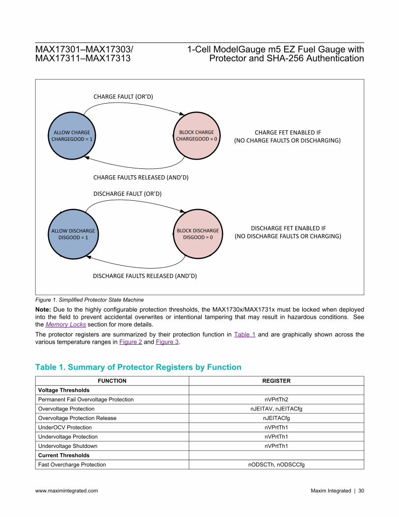
CHARGE FAULT (OR’D)
CHARGE FAULTS RELEASED (AND’D)
DISCHARGE FAULT (OR’D)
DISCHARGE FAULTS RELEASED (AND’D)
CHARGE FET ENABLED IF (NO CHARGE FAULTS OR DISCHARGING)
DISCHARGE FET ENABLED IF (NO DISCHARGE FAULTS OR CHARGING)
ALLOW CHARGECHARGEGOOD = 1
BLOCK CHARGECHARGEGOOD = 0
BLOCK DISCHARGEDISGOOD = 0
ALLOW DISCHARGEDISGOOD = 1
Figure 1. Simplified Protector State Machine
Note: Due to the highly configurable protection thresholds, the MAX1730x/MAX1731x must be locked when deployed into the field to prevent accidental overwrites or intentional tampering that may result in hazardous conditions. See the Memory Locks section for more details. The protector registers are summarized by their protection function in Table 1 and are graphically shown across the various temperature ranges in Figure 2 and Figure 3.
Table 1. Summary of Protector Registers by Function FUNCTION REGISTER
Voltage Thresholds Permanent Fail Overvoltage Protection nVPrtTh2 Overvoltage Protection nJEITAV, nJEITACfg Overvoltage Protection Release nJEITACfg UnderOCV Protection nVPrtTh1 Undervoltage Protection nVPrtTh1 Undervoltage Shutdown nVPrtTh1 Current Thresholds Fast Overcharge Protection nODSCTh, nODSCCfg
MAX17301–MAX17303/MAX17311–MAX17313
1-Cell ModelGauge m5 EZ Fuel Gauge withProtector and SHA-256 Authentication
www.maximintegrated.com Maxim Integrated | 30

Table 1. Summary of Protector Registers by Function (continued) Slow Overcharge Protection nIPrtTh1 Slow Overdischarge Protection nIPrtTh1 Fast Overdischarge Protection nODSCTh, nODSCCfg Short Circuit Protection nODSCTh, nODSCCfg Charging Detected nProtMiscTh Discharging Detected nProtMiscTh Temperature Thresholds nTPrtTh1, nTPrtTh2, nTPrtTh3, nProtMiscTh Fault Timers nDelayCfg Charging Prescription Charging Voltage nJEITAV Charging Current nJeitaC Precharge Current nJEITACfg Step Charging nStepChg Protection Status/Configuration nProtCfg, ProtStatus, nBattStatus
MAX17301–MAX17303/MAX17311–MAX17313
1-Cell ModelGauge m5 EZ Fuel Gauge withProtector and SHA-256 Authentication
www.maximintegrated.com Maxim Integrated | 31

TEMPERATURE
CEL
L VO
LTAG
E
T4 (T
OO
HO
T)
T3 (H
OT)
T2 (C
OLD
)
T1 (T
OO
CO
LD)
-10 10 45 60
PERM FAIL OVP
UV PROTECTION
4.4V
4.35V
2.8V
3.0VVEMPTY
JEITA CHARGE VOLTAGE
STEPV0
STEPV1
STEPV2
STEP
DV0
STEP
DV1
DESIGN VOLTAGE3.7V
MINIMUM OPERATING VOLTAGE
2.3VUV SHUTDOWN
ROOMCOLD HOTTOO COLD
2.7V
STEP-CHARGINGSTEP-CHARGING
80
TWA
RM
TOO
HO
T D
ISC
HA
RG
E
DIE
TEM
P H
OT
WARM TOO HOT
35 75
PER
M F
AIL
OTP
OVERVOLTAGE PROTECTION
OVP RELEASE
CHARGING VOLTAGE
4.25V
4.2V
70
2.9VUOCV PROTECTION
Figure 2. Programmable Voltage Thresholds
MAX17301–MAX17303/MAX17311–MAX17313
1-Cell ModelGauge m5 EZ Fuel Gauge withProtector and SHA-256 Authentication
www.maximintegrated.com Maxim Integrated | 32

3500mAFAST OVERCHARGE PROTECTION
TEMPERATURE
T4 (T
OO
HO
T)
T3 (H
OT)
T2 (C
OLD
)
T1 (T
OO
CO
LD)
-10 10 45 60
3000mASLOW OVERCHARGE
PROTECTION
ROOMCOLD HOT
STEP-CHARGINGSTEP-CHARGING
TOO
HO
T D
ISC
HA
RG
E
DIE
TEM
P H
OT
WARM TOO HOT
35
PER
M F
AIL
OTP
SHORT CIRCUIT PROTECTION-5000mA
-4000mAFAST OVERDISCHARGE PROTECTION
DIS
CH
ARG
ING
CU
RR
ENT
SLOW OVERDISCHARGE PROTECTION-3000mA
CH
ARG
ING
CU
RR
ENT
CHARGING CURRENT
STEPCURR1
STEPCURR2TOO COLD
2000mACHARGING CURRENT
100mAPRECHARGE
10mA CURRDET
70 75 80
TWA
RM
Figure 3. Programmable Current Thresholds
Protector Thresholds The MAX1730x/MAX1731x provides for a variety of programmable protector thresholds that are stored in nonvolatile memory. These thresholds include voltage, current, temperature, and timer delays.
Voltage Thresholds All voltage thresholds of the MAX1730x/MAX1731x are shown graphically in Figure 2 and in table form with details of which bits and registers create the various thresholds in Table 2. The description of each register provides additional guidance for selection of the register value.
MAX17301–MAX17303/MAX17311–MAX17313
1-Cell ModelGauge m5 EZ Fuel Gauge withProtector and SHA-256 Authentication
www.maximintegrated.com Maxim Integrated | 33

Table 2. Voltage Thresholds
NAME DESCRIPTION CONFIGURATION REGISTERS EXAMPLE
Permanent Fail Overvoltage nVPrtTh2.OVP_PermFail 4.4V
Overvoltage (with 4xJEITA)
Programmable overvoltage at each JEITA band. Programmable 10mV resolution from 3.9V to 4.88V. Programmable delay.
ChargeVoltage[temp] + nJEITACfg.dOVP
4.1V/4.20V/4.18/
4.15V +50mV
Overvoltage Release Programmable release hysteresis Overvoltage - JEITACfg.dOVPR
4.15V/4.25V/4.23V/4.2V
-10mV ChargeVoltage-Room ChargingVoltage() output nJEITAV.Room 4.20V ChargeVoltage-Hot ChargingVoltage() output nJEITAV.Hot 4.15V ChargeVoltage-Warm ChargingVoltage() output nJEITAV.Warm 4.18V ChargeVoltage-Cold ChargingVoltage() output nJEITAV.Cold 4.10V DesignVoltage Just for information, no action nDesignVolt 3.7V EmptyVoltage For fuel gauge only (not related to protection) nVEmpty 3.0V Undervoltage Release Charger applied Under OCV Protection (SmartEmpty)
Programmable under-OCV 40mV steps UVP to UVP + 1.28V. nVPrtTh1.UOCVP 3.2V
Undervoltage Protection Programmable undervoltage 20mV steps 2.2V to 3.4V. Gauging and communications work until undervoltage-shutdown
nVPrtTh1.UVP 2.7V
Undervoltage Shutdown Gauging and communications work until undervoltage-shutdown nVPrtTh1.UVShdn 2.5V
Hardware Startup 2.1V typ, 2.3V max
Low-Voltage Charging 1.8V Zero-Voltage Charging 0.0V
Ideal Diode Behavior The IC uses several methods to detect charge and discharge to provide the following "Ideal Diode" discharge control without forgetting a possible charge fault state such as OVP, OTP, or UTP (overcharge current is fully released during a discharge condition).
1. Fast On. When discharge is detected, the CHG FET quickly turns on regardless of any charge fault condition. This limits the heat and voltage drop associated with the 0.6V CHG FET body diode.
1. Current < -CurrDet. nProtMiscTh.CurrDet is normally configured to 2 to provide a clear threshold relative to ADC noise. With a 10mΩ sense resistor, this corresponding to 7.5mA, provides sufficient sensitivity for most active loads.
2. PCKP < BATT +0.1V (falling only). Additionally, a comparator detects charger removal to support better discharging detection even during small standby currents.
2. Fast Off. When discharge to charge transition is detected while a charge fault (such as OTP/OVP/UTP) remains latched, the CHG FET quickly turns off to prevent charging. Since the charge fault remains
MAX17301–MAX17303/MAX17311–MAX17313
1-Cell ModelGauge m5 EZ Fuel Gauge withProtector and SHA-256 Authentication
www.maximintegrated.com Maxim Integrated | 34

remembered (not released by the discharging), the response happens quickly without waiting for double-confirmation by the fault timer.
3. Slow On. Smaller standby currents require the sensitivity provided by the filter of the AvgCurrent register. 1. AvgCurrent < -AvgCurrDet. For default configuration and with 10mΩ, AvgCurrDet is sensitive to
1.4mA discharge. The AvgCurrDet threshold follows the filter configuration nFilterCfg.nCurr as well as the hibernate state and configuration according Table 3 when using default nProtMiscTh.CurrDet = 7.5mA.
Table 3. AvgCurrDet Threshold When Using 10mΩ and Default nProtMiscTh.CurrDet = 7.5mA AVGCURRENT FILTER CONFIGURATION (nFilterCfg.nCurr) 1 (0.7s) 2 (1.4s) 3 (2.8s) 4 (5.6s) 5 (11.25s) 6 (22.5s) 7 (45s) 8 (90s) Active (0.351s) 4.22mA 2.34mA 2.34mA 1.41mA 1.41mA 0.94mA 0.94mA 0.7mA Hibernate (1.4s) 7.5mA 4.2mA 4.2mA 2.3mA 2.3mA 1.4mA 1.4mA 0.94mA Hibernate (2.8s) 7.5mA 7.5mA 7.5mA 4.2mA 4.2mA 2.3mA 2.3mA 1.4mA
4. Slow Off. AvgCurrent > -0.3mA. While the Charge Fault remains, the CHG FET turns off whenever AvgCurrent fails to exceed the more sensitive -0.3mA discharge threshold.
The fast responses in Table 3 correspond with the 0.351s ADC update rate. The more accurate slow responses correspond with the AvgCurrent filter delay configuration.
Current Thresholds All of the current thresholds of the MAX1730x/MAX1731x are shown graphically in Figure 3 and in table form with details of each threshold in Table 4. The description of each register provides additional guidance for selection of the register value.
Table 4. Current Threshold Summary CURRENT ACTION RELEASE DETAILS
Overcharge Current (fast) CHG off
Discharging or charger removal detection
Threshold 5-bit, 1.25mV steps to 38.75mV. Delay programmable 4-bit, 1ms to 15ms in 0.9ms steps.
Overcharge Current (slow with 4xJEITA)
CHG off Programmable 0.4mV steps to 51.2mV. Delay programmable 351ms to 45s. Separate thresholds for 4 out of 6 JEITA segments.
Overdischarge Current (fast) DIS off
Charging or load removal detection
5-Bit, 2.5mV steps to 77.5mV. Delay programmable 4-bit, 1ms to 15ms in 0.9ms steps.
Overdischarge Current (slow) DIS off Programmable 0.4mV steps to 51.2mV. Delay programmable 351ms to
45s. Short-Circuit Current DIS off 5-Bit, 5mV steps to 155mV.
Delay programmable 4-bit, 70μs steps to 985μs. Charging Detected Normal Current > CurrDet or AvgCurrent > AvgCurrDet or PCKP > BATT +
0.15V to release overdischarge protection.
MAX17301–MAX17303/MAX17311–MAX17313
1-Cell ModelGauge m5 EZ Fuel Gauge withProtector and SHA-256 Authentication
www.maximintegrated.com Maxim Integrated | 35

Table 4. Current Threshold Summary (continued)
Discharging Detected Normal
Current < -CurrDet or AvgCurrent < -AvgCurrDet or PCKP < BATT + 0.15V (falling-edge) indicates discharging. When discharging is detected, overcharge current faults release. Other charge faults such as OVP, OTP, UTP remain set, however, the CHG FET turns on to prevent the heat and voltage drop associated with the 0.6V CHG FET body diode. See the Ideal Diode Behavior section for more details. An OVP fault remains remembered (unreleased) until voltage falls and discharging is also detected.
Overcurrent Protection The MAX1730x/MAX1731x provides three levels of protection for overdischarge current events: fast, medium, and slow as shown in Figure 4. The MAX1730x/MAX1731x also provides fast and slow levels of protection for overcharge current protection. The fast and medium levels of protection are provided by comparators and the slow levels are based on the ADC readings. The MAX1730x/MAX1731x maintains the protection until the source of the fault has been removed. Overcharge protection fault releases when pack voltage falls below BATT + 0.1V (edge, not level) while the IC tests charger removal by applying a 40kΩ pull down from PCKP to GND (during any charger fault). Overdischarge current (fast or slow) or short-circuit current protection faults release when PCKP rises above 1V, while the IC applies 30μA source current test to PCKP.
DEBOUNCE TIME
DIS
CH
AR
GE
CU
RR
ENT
OVERDISCHARGE THRESHOLDNODSCTH.ODTH (0-77.5mV)
OV
ERD
ISCH
AR
GE D
ELAY
NO
DSC
CFG
.OD
DLY (1
.05
ms - 1
4.6
6m
s)
MEDIUM(MILLISECONDS)
SLOW (SECONDS, WITH 1% ACCURACY)
ADC OVERDISCHARGE THRESHOLDNIPRTTH1.ODCP (0-51.2mV) A
DC
OV
ERC
UR
REN
T DELA
Y N
DELA
YCFG
.OV
ERC
UR
RTIM
ER(0
.35
1s to
22
.5s)
SHO
RT-C
IRC
UIT D
ELAY
NO
DSC
CFG
.SCD
LY (13
1µ
s TO 9
85
µs)
SHORT-CIRCUIT THRESHOLDNODSCTH.SCTH (0-155mV)
FAST(MICROSECONDS)
Figure 4. Fast, Medium, and Slow Overdischarge Protection
MAX17301–MAX17303/MAX17311–MAX17313
1-Cell ModelGauge m5 EZ Fuel Gauge withProtector and SHA-256 Authentication
www.maximintegrated.com Maxim Integrated | 36

Fast Overcurrent Comparators The MAX1730x/MAX1731x contains three programmable fast overcurrent comparators called Overdischarge (OD), Short-Circuit (SC), and Overcharge (OC) that allow control protection for overdischarge current, short-circuit current, and overcharge current. These comparators have programmable threshold levels and programmable debounced delays. See Figure 5. The OD comparator threshold can be programmed from 0mV to -77.5mV with 2.5mV resolution (0 to -7.75A with 0.25A resolution using 10mΩ sense resistor). The OC comparator threshold can be programmed from 0mV to 38.75mV with 1.25mV resolution (0 to 38.75A with 0.125A resolution using 10mΩ sense resistor). The OD and OC comparators have a programmable delay from 1.05ms to 14.6ms with 0.97ms resolution. The SC comparator threshold can be programmed from 0mV to -155mV with 5mV resolution (0 to -15.5A with 0.5A resolution using 10mΩ sense resistor), and has a programmable delay from 70μs to 985μs with a 61μs resolution. The nODSCTh register sets the threshold levels where each comparator trips. The nODSCCfg register enables each comparator and sets their debounce delays. The nODSCCfg register also maintains indicator flags of which comparator has been tripped. These register settings are maintained in nonvolatile memory if the nNVCfg1.enODSC bit is set.
Overcurrent Comparator Diagram
ODi
+
-
-
RSENSE
CSP CSN
ODTH
OCi+
-
OCTHOCDLY
OCDLY
ODSCCfg
SCi
+
-SCTHSCDLY
Figure 5. Overcurrent Comparator Diagram
Slow Overcurrent Protection The MAX1730x/MAX1731x provides programmable thresholds for the slow overdischarge current protection (ODCP) and overcharge current protection (OCCP). ODCP and OCCP can be configured to provide different levels of protection across the six temperature zones as shown in Figure 3.
Temperature Thresholds The six temperature zones shown in Figure 2 and Figure 3 can be configured in the nTPrtTh1, nTPrtTh2, and nTPrtTh3 registers.
MAX17301–MAX17303/MAX17311–MAX17313
1-Cell ModelGauge m5 EZ Fuel Gauge withProtector and SHA-256 Authentication
www.maximintegrated.com Maxim Integrated | 37

Other Thresholds
Table 5. Other Thresholds THRESHOLD ACTION CONDITIONS
Charge Suspend CHG off
FullDet Fault—if enabled (nProtCfg.FullEn) and charge termination criteria (see ICHGTerm and charge termination). ChgWDT Fault—if enabled (nProtCfg.ChgWDTEn) and communications timeout.
Charge-Suspend Release Normal
FullDet Release—Discharge or charger removal detected. ChgWDT Release—Communications or discharge or charger removal detected.
Charge FET Failure Blow fuse CHG off yet charge-current persists (programmable).
Discharge FET Failure Blow fuse DIS off yet discharge-current persists (programmable).
Charge Voltage/Current "Prescription" Six-zone JEITA (four charge currents and voltages).
Disabling FETs by Pin-Control or I2C Command The IC provides FET override control by either I2C command or pin-command to the ALRT pin. This functionality can be useful for various types of applications: Factory Testing. Disconnecting the battery is useful for testing with a controlled external power supply. Battery Selection. In a multiple battery system, one battery can be disconnected and another connected by
operating the FETs. When allowed by nonvolatile configuration, both FETs can be turned off by pin control or either FET can be individually turned off by I2C command. The control operates as follows: ALRT Pin Override. Set nProtCfg.OvrdEn = 1 and drive ALRT low to force both FETs into the off state. Releasing
the ALRT line recovers the FETs according to the protector's fault state machine. I2C Command Override. Set nProtCfg.CmOvrdEn = 1 and write CommStat.CHGOff or CommStat.DISOff to
independently disable either the charge or discharge FET. Clearing CHGOff and DISOff recovers the FETs according to the protector's fault state machine.
These features may be disabled and locked by nonvolatile memory to prevent malicious code from blocking the FETs. Although disabling FETs does not produce any safety issue, it can be a nuisance if malicious system-side software denies power to the system.
Charging Prescription The MAX1730x/MAX1731x can guide a charger with recommended charging voltage and charging current to safely charge the battery depending on the state of the battery and the temperature. The ChargingVoltage and ChargingCurrent registers provide the information according to the recommended charging based on knowledge that is installed in the battery under the principle that the battery maker knows the requirements best. This information can be stored in the MAX1730x/MAX1731x to provide the factory recommended charging current and voltage. This is useful when a system involves multiple battery vendors, swappable batteries, aftermarket batteries, or legacy system support. As the temperature of the battery changes significantly above and below room temperature, most cell manufacturers recommend to charge at reduced current and lower termination voltage to assure safety and improve lifespan. The MAX1730x/MAX1731x can be configured to change its guidance according to TooCold/Cold/Room/Warm/Hot/TooHot programmable temperature regions (see nTPrtTh1/2/3). Both charging current and voltage are updated at Cold/Warm/Hot (see nJEITAV and nJEITAC). See Figure 2 and Figure 3.
MAX17301–MAX17303/MAX17311–MAX17313
1-Cell ModelGauge m5 EZ Fuel Gauge withProtector and SHA-256 Authentication
www.maximintegrated.com Maxim Integrated | 38

Additionally, the IC provides step-charging to improve lifespan of the battery and charge speed by applying a step-charging profile (see the Step-Charging section) as shown in Figure 6.
Step Charging A step-charging profile sets three charge voltages, three corresponding charge currents, and manages a state-machine to trace through the stages as shown in Figure 6.
SOC
SOC
90%
VCELL
VCELL
50%
30%
TH1 = FULL VOLTAGE - STEPDV1
0 1 2VCELL > TH0 VCELL > TH1
NOT CHARGING/DISCHARGING
NOT CHARGING/DISCHARGING
FULL VOLTAGE
HIGHEST CURRENT, LOWEST VOLTAGE
MEDIUM CURRENT REDUCED CURRENT UNTIL FULL
TH0 = FULL VOLTAGE – STEPDV0
PROTTMRSTAT.CHARGESTEP
Figure 6. Step-Charging State Machine
This breaks charging into three regions: Region 0: Highest current, lowest voltage. ChargingCurrent comes from nJEITAC until VCell > StepVolt0. After VCell > StepVolt0, ChargingCurrent becomes defined by Region 1. Region 1: Medium current. ChargingCurrent comes from nJEITAC x (StepCurr1 + 1)/16, which is a ratio from 1/16 to 16/16 until VCell > StepVolt1. When VCell > StepVolt1, ChargingCurrent becomes defined by Region 2. Region 2: Reduced current until full. ChargingCurrent comes from nJEITAC x (StepCurr2 + 1)/16, which is a ratio from 1/16 to 16/16 until full. For example, a charge may start with a ChargingCurrent of 2000mA until the cell voltage reaches 4.12V. At that point, the ChargingCurrent is reduced to 1000mA until the cell voltage reaches 4.16V. Then, the ChargingCurrent is further reduced to 500mA where it remains until the current begins to taper off naturally to the termination current.
Zero-Volt Charging When in undervoltage protection, the MAX1730x/MAX1731x turns both FETs off and then enters a low quiescent state. After a long time in the undervoltage state, it is possible for the battery voltage to fall below the minimum 2.3V operating voltage, making it unable to wakeup by communications or pushbutton. In this situation, an external charge voltage must be applied to PCKP in order to wake up the IC. The IC supports two options to recover an overdischarged battery according to the ZVC pin voltage:
MAX17301–MAX17303/MAX17311–MAX17313
1-Cell ModelGauge m5 EZ Fuel Gauge withProtector and SHA-256 Authentication
www.maximintegrated.com Maxim Integrated | 39

1. Zero-Volt Charge Recovery. In this configuration (connect ZVC to GND), even a battery at zero volts can be charged by applying a charger at PCKP. If a secondary protector is used, zero-volt charge recovery must be enabled.
There are three phases for 0V recovery charge as shown in Figure 7. Phase 1. VBATT ≤ max(1.8V, VGS). Low battery recovery charge phase. CHG is shorted to PCKP. PCKP
voltage is clamped to VGS_CHG + VBATT. Phase 2. max(1.8V, VGS) ≤ VBATT. Charge pump recovery charge phase. CHG is powered by the charge
pump and CHG driver. This phase begins when VBATT exceeds the FET's Vt threshold. The IC detects that the pump voltage is sufficient to drive the gate.
Phase 3. VBATT > 2.1V. The IC wakes up, begins ADC readings, and resumes normal protection functionality.
0V
VtCHG
1.8V
2.3V
VPCKP
VBATT
PHASE 1 PHASE 2 PHASE 3
VPCKP = VBATT + VtCHG
BODY-DIODE DROP OF DIS FET
CHARGE PUMP ON NORMAL PROTECTOR OPERATION
Figure 7. Zero-Volt Recovery Charge
2. 1.8V Charge Recovery. In this configuration, a battery below 1.8V permanently rejects charge. This has some safety benefit for some Lithium batteries, since very low voltage can cause copper-deposition creating an unsafe state in the battery. If the cell is above 1.8V, then charge recovery begins in Phase 2 whenever a charger is applied at PCKP.
If the cell voltage is less than 1.8V, then the MAX1730x/MAX1731x connects PCKP to CHG as shown in Figure 8. VPCKP becomes VBATT + VTCHG. This connection persists until the CP charge pump is enabled at approximately 1.8V. VPCKP voltage varies based on the VGS of the external CHG FET. At this time, PCKP disconnects from CHG and the device resumes normal protection operation. Note: To ensure that a pack can be recovered from low voltage, the Vt of the CHG FET must be less than Charger's Voltage/2.
MAX17301–MAX17303/MAX17311–MAX17313
1-Cell ModelGauge m5 EZ Fuel Gauge withProtector and SHA-256 Authentication
www.maximintegrated.com Maxim Integrated | 40

MAX1730XMAX1731X
N N
CHG DIS PCKPZERO-VOLT CHARGE
CONNECTION
VDIODE
VGS
BATT
CP
PCKP
Figure 8. Zero-Volt Charging Diagram
ModelGauge m5 Algorithm Classical coulomb-counter-based fuel gauges have excellent linearity and short-term performance. However, they suffer from drift due to the accumulation of the offset error in the current-sense measurement. Although the offset error is often very small, it cannot be eliminated, causes the reported capacity error to increase over time, and requires periodic corrections. Corrections are usually performed at full or empty. Some other systems also use the relaxed battery voltage to perform corrections. These systems determine the true state-of-charge (SOC) based on the battery voltage after a long time of no current flow. Both have the same limitation; if the correction condition is not observed over time in the actual application, the error in the system is boundless. The performance of classic coulomb counters is dominated by the accuracy of such corrections. Voltage measurement based SOC estimation has accuracy limitations due to imperfect cell modeling, but does not accumulate offset error over time. The IC includes an advanced voltage fuel gauge (VFG), which estimates OCV, even during current flow, and simulates the nonlinear internal dynamics of a Li+ battery to determine the SOC with improved accuracy. The model considers the time effects of a battery caused by the chemical reactions and impedance in the battery to determine SOC. This SOC estimation does not accumulate offset error over time. The IC performs a smart empty compensation algorithm that automatically compensates for the effect of temperature condition and load condition to provide accurate state-of-charge information. The converge-to-empty function eliminates error toward empty state. The IC learns battery capacity over time automatically to improve long-term performance. The age information of the battery is available in the output registers. The ModelGauge m5 algorithm combines a high-accuracy coulomb counter with a VFG. See Figure 9. The complementary combined result eliminates the weaknesses of both the coulomb counter and the VFG while providing the strengths of both. A mixing algorithm weighs and combines the VFG capacity with the coulomb counter and weighs each result so that both are used optimally to determine the battery state. In this way, the VFG capacity result is used to continuously make small adjustments to the battery state, canceling the coulomb-counter drift.
MAX17301–MAX17303/MAX17311–MAX17313
1-Cell ModelGauge m5 EZ Fuel Gauge withProtector and SHA-256 Authentication
www.maximintegrated.com Maxim Integrated | 41

COULOMB COUNTER
CAPACITY
ΔQ
FULL, EMPTY, AND STANDBY STATE DETECTION
UNNECESSARY
MODELGAUGE
Δ% SOC
MICRO-CORRECTIONS
VERY SLOW INFLUENCE
Figure 9. Merger of Coulomb Counter and Voltage Based Fuel Gauge
The ModelGauge m5 algorithm uses this battery state information and accounts for temperature, battery current, age, and application parameters to determine the remaining capacity available to the system. As the battery approaches the critical region near empty, the ModelGauge m5 algorithm invokes a special error correction mechanism that eliminates any error. The ModelGauge m5 algorithm continually adapts to the cell and application through independent learning routines. As the cell ages, its change in capacity is monitored and updated and the voltage-fuel-gauge dynamics adapt based on cell-voltage behavior in the application.
MAX17301–MAX17303/MAX17311–MAX17313
1-Cell ModelGauge m5 EZ Fuel Gauge withProtector and SHA-256 Authentication
www.maximintegrated.com Maxim Integrated | 42

+- +
×
OCV CALCULATION
OCV OUTPUT
VOLTAGE
CAPACITY LEARNmAh PER PERCENT
RELAXED CELL
DETECTION
OCV TEMPERATURE
COMPENSATIONLEARN
OCV TABLE LOOKUP % REMAINING
OUTPUT
COULOMB COUNTER mAH OUTPUT
CURRENT
TIME
APPLICATION OUTPUTS:
REPSOC REGISTERREPCAP REGISTERAVSOC REGISTERAVCAP REGISTERTTE / AtTTE / TTF REGISTERSFULLCAP REGISTER
END OF CHARGE DETECTION
APPLICATON EMPTY
COMPENSATION BASED ON APPLICATION
TEMPERATURE AND DISCHARGE RATE
MIXING ALGORITHM mAH OUTPUT
MIXCAP REGISTERMIXSOC REGISTER
CELL CHEMISTRY OUTPUTS:
VFOCV REGISTERCYCLES REGISTERRFAST REGISTERFULLCAPNOM REGISTERAGE REGISTER
EMPTY DETECTION
EMPTY COMPENSATION
LEARNING
Figure 10. ModelGauge m5 Block Diagram
Wakeup/Shutdown
Modes of Operation The MAX1730x/MAX1731x supports six power modes (three active modes and three shutdown modes) as shown in Table 6 with descriptions of the features available in each mode, the typical current consumption of each mode, and the method to enter and exit each mode.
MAX17301–MAX17303/MAX17311–MAX17313
1-Cell ModelGauge m5 EZ Fuel Gauge withProtector and SHA-256 Authentication
www.maximintegrated.com Maxim Integrated | 43

Table 6. Modes of Operation
MODE CONSUMPTION (TYPICAL) (μA) DESCRIPTION
Active 24 Full Functionality. Protection FETs, charge pump, and ADC are on. Firmware tasks execute every 351ms.
Hibernate (optional) 18
FETs, charge pump, and ADC are on. Firmware tasks execute every 1.4s. If enabled, the device automatically enters and exits this mode depending on current measurements. Entering hibernate mode requires a low-enough current for a long-enough duration. Exiting requires just one high-enough current event. For specific details regarding the thresholds, see nHibCfg register definition.
Protect 10
ADC is on. FETs and charge pump are disabled due to a protection event, disconnecting the battery from the system. RAM is preserved and the gauge continues to monitor the battery until the fault is removed. Firmware remains awake and ready to communicate. Firmware tasks execute every 1.4s.
Ship*
10
Similar state as "Protected and Awake" except the firmware is responsive to wakeup events such as: charger-connection, communications-wakeup, or pushbutton wakeup (depending on which wakeups are enabled by configuration). Firmware tasks execute every 1.4s.
7
Similar state as "Protected and Awake" except the firmware is responsive to wakeup events such as: charger-connection, communications-wakeup, or pushbutton wakeup (depending on which wakeups are enabled by configuration). Firmware tasks execute every 5.625s.
DeepShip* 0.5
FETs, charge pumps, ADC, and firmware are all placed into a shutdown state. The only activity alive relates to analog circuits that monitor for wakeup conditions (charger-detection, communications, or pushbutton, depending on which are enabled).
Undervoltage Shutdown 0.1
FETs, charge pumps, ADC, firmware, and most wakeup circuits are powered down. Only the charger-detection wakeup circuit remains powered in this mode to best conserve the small remaining battery capacity and prevent deep discharge.
*On I2C shutdown command or when I2C SCL/SDA lines collapse (and depending on whether COMMSH is enabled), the MAX1730x/MAX1731x either enters Ship (if nProtCfg.DeepShpEn = 0) or DeepShip (if nProtCfg.DeepShpEn = 1). The MAX1730x/MAX1731x can be awoken with a variety of methods depending on the configuration. If pushbutton wakeup is enabled (nConfig.PBen = 1), then consistently pulling the ALRT/PIO pin low, either by pushbutton or system configuration will wakeup the device. A high to low transition on any of the communication lines will wake up the device. A consistent connection to a charger will wake up the device. The MAX1730x/MAX1731x prevents accidental wakeup when the system is boxed and shipped. When awoken by any source, it debounces all wakeup sources (button, communications, and charger-detection) to ensure that the wakeup is valid. If no valid wakeup is discovered, the device returns to Ship or DeepShip. The IQ in the active, hibernate, and ship modes are impacted by the configuration of the IC. Table 7 shows the recommended configuration settings for the nConfig register and the impact those settings have on the IQ of each mode. Note that when in hibernate mode, the protection for overtemperature and overvoltage are delayed by the nHibCfg.HibScalar value. It is not recommended to have hibernation enabled with the nHibCfg.HibScalar set to more than 1.4 seconds.
MAX17301–MAX17303/MAX17311–MAX17313
1-Cell ModelGauge m5 EZ Fuel Gauge withProtector and SHA-256 Authentication
www.maximintegrated.com Maxim Integrated | 44
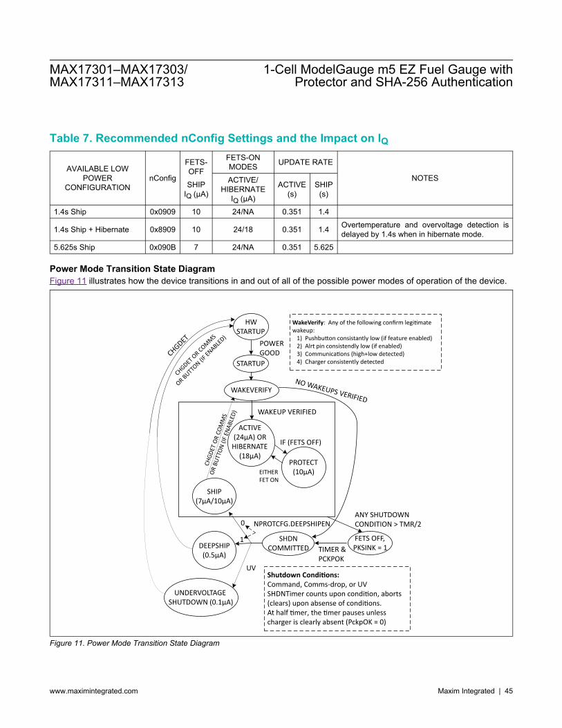
Table 7. Recommended nConfig Settings and the Impact on IQ
AVAILABLE LOW POWER
CONFIGURATION nConfig
FETS-OFF SHIP
IQ (μA)
FETS-ON MODES UPDATE RATE
NOTES ACTIVE/HIBERNATE
IQ (μA)
ACTIVE (s)
SHIP (s)
1.4s Ship 0x0909 10 24/NA 0.351 1.4
1.4s Ship + Hibernate 0x8909 10 24/18 0.351 1.4 Overtemperature and overvoltage detection is delayed by 1.4s when in hibernate mode.
5.625s Ship 0x090B 7 24/NA 0.351 5.625
Power Mode Transition State Diagram Figure 11 illustrates how the device transitions in and out of all of the possible power modes of operation of the device.
STARTUP
PROTECT (10µA)
SHIP (7µA/10µA)
DEEPSHIP (0.5µA)
HW STARTUP
NPROTCFG.DEEPSHIPEN
1
0
ACTIVE (24µA) OR
HIBERNATE (18µA)
UNDERVOLTAGE SHUTDOWN (0.1µA)
FETS OFF, PKSINK = 1
UV
ANY SHUTDOWN CONDITION > TMR/2
POWER GOOD
IF (FETS OFF)
EITHER FET ON
Shutdown Conditions: Command, Comms-drop, or UVSHDNTimer counts upon condition, aborts (clears) upon absense of conditions.At half timer, the timer pauses unless charger is clearly absent (PckpOK = 0)
TIMER & PCKPOK
CHGDET
CHGDET OR C
OMM
S
OR BUTTO
N (IF E
NABLED)
CH
GD
ET O
R C
OM
MS
OR
BU
TTO
N (I
F EN
AB
LED
)
WAKEVERIFY
SHDN COMMITTED
NO WAKEUPS VERIFIED
WakeVerify: Any of the following confirm legitimate wakeup: 1) Pushbutton consistantly low (if feature enabled) 2) Alrt pin consistendly low (if enabled) 3) Communications (high+low detected) 4) Charger consistently detected
WAKEUP VERIFIED
Figure 11. Power Mode Transition State Diagram
MAX17301–MAX17303/MAX17311–MAX17313
1-Cell ModelGauge m5 EZ Fuel Gauge withProtector and SHA-256 Authentication
www.maximintegrated.com Maxim Integrated | 45
Pushbutton Wakeup The ALRT/PIO pin can be used to wake up the device by enabling the pushbutton wakeup function by setting the nConfig.PBen. The pushbutton can be implemented in the system to wakeup the device and the system as shown in the Pushbutton Schematic.
Register Description Conventions The following sections define standard conventions used throughout the data sheet to describe register functions and device behavior. Any register that does not match one of the following data formats is described as a special register.
Standard Register Formats Unless otherwise stated during a given register's description, all IC registers follow the same format depending on the type of register. Refer to Table 8 for the resolution and range of any register described hereafter. Note that current and capacity values are displayed as a voltage and must be divided by the sense resistor to determine amps or amp-hours. It is strongly recommended to use the nRSense (1CFh) register to store the sense resistor value for use by host software.
Table 8. ModelGauge Register Standard Resolutions REGISTER
TYPE LSB SIZE MINIMUM VALUE
MAXIMUM VALUE NOTES
Capacity 5.0μVh/ RSENSE
0.0μVh 327.675mVh/ RSENSE
Equivalent to 0.5mAh with a 0.010Ω sense resistor.
Percentage 1/256% 0.0% 255.9961% 1% LSb when reading only the upper byte. Voltage 0.078125mV 0.0V 5.11992V
Current 1.5625μV/ RSENSE
-51.2mV/ RSENSE
51.1984mV/ RSENSE
Signed 2's complement format. Equivalent to 156.25μA with a 0.010Ω sense resistor.
Temperature 1/256°C -128.0°C 127.996°C Signed 2's complement format. 1°C LSb when reading only the upper byte.
Resistance 1/4096Ω 0.0Ω 15.99976Ω Time 5.625s 0.0s 102.3984hr Special Format details are included with the register description.
Device Reset Device reset refers to any condition that would cause the IC to recall nonvolatile memory into RAM locations and restart operation of the fuel gauge. Device reset refers to initial power up of the IC, temporary power loss, or reset through the software power-on-reset command.
Nonvolatile Backup and Initial Value All configuration register locations have nonvolatile memory backup that can be enabled with control bits in the nNVCfg0, nNVCfg1, and nNVCfg2 registers. If enabled, these registers are initialized to their corresponding nonvolatile register value after device reset. If nonvolatile backup is disabled, the register restores to an alternate initial value instead. See each register description for details.
MAX17301–MAX17303/MAX17311–MAX17313
1-Cell ModelGauge m5 EZ Fuel Gauge withProtector and SHA-256 Authentication
www.maximintegrated.com Maxim Integrated | 46

Register Naming Conventions Register addresses are described throughout the document as 9-bit internal values from 000h to 1FFh. These addresses must be translated to 16-bit external values for the MAX17301-MAX17303 (I2C) or 8-bit values for the MAX17311-MAX17313 (1-Wire). See the Memory section for details. Register names that start with a lower case 'n', such as nPackCfg for example, indicate the register is a nonvolatile memory location. Register names that start with a lower case 's' indicate the register is part of the SBS compliant register block.
Protection Registers
Voltage Protection Registers
nVPrtTh1 Register (1D0h) Register Type: Special The nVPrtTh1 register shown in Table 9 sets undervoltage protection, deep-discharge-state protection, and undervoltage-shutdown thresholds.
Table 9. nVPrtTh1 Register (1D0h) Format D15 D14 D13 D12 D11 D10 D9 D8 D7 D6 D5 D4 D3 D2 D1 D0
UVP UOCVP UVShdn
UVP: Undervoltage Protection Threshold. The MAX1730x/MAX1731x opens the discharge FET when VCell < UVP. UVP can be configured from 2.2V to 3.46V in 20mV steps. UVP is unsigned. UOCVP: Under Open Circuit Voltage Protection Threshold (also referred to as SmartEmpty). The MAX1730x/MAX1731x opens the discharge FET when VFOCV < UOCVP. UOCVP is relative to UVP and can be configured from UVP to UVP + 1.28V in 40mV steps. UVShdn: Undervoltage Shutdown Threshold. The MAX1730x/MAX1731x shutdowns when VCell < UVShdn. UVShdn is relative to UVP and can be configured from UVP - 0.32V to UVP + 0.28V in 40mV steps. Note that this is a signed value and UVShdn should be configured as a 2's compliment negative value so that UVShdn < UVP.
nVPrtTh2 Register (1D4h) Register Type: Special The nVPrtTh2 register shown in Table 10 sets permanent-failure-overvoltage-protection and prequalification voltage thresholds. Threshold limits are configurable with 20mV resolution over the full operating range of the VCell register.
Table 10. nVPrtTh2 Register (1D4h) Format D15 D14 D13 D12 D11 D10 D9 D8 D7 D6 D5 D4 D3 D2 D1 D0
OVP_PermFail Reserved
OVP_PermFail: Permanent Failure OVP (overvoltage protection) threshold. Permanent Failure Overvoltage protection occurs when VCell register reading exceeds this value.
nJEITAV Register (1D9h) nJEITAV Register, shown in Table 11, sets the JEITA charge voltage configuration for the MAX1730x/MAX1731x. The
MAX17301–MAX17303/MAX17311–MAX17313
1-Cell ModelGauge m5 EZ Fuel Gauge withProtector and SHA-256 Authentication
www.maximintegrated.com Maxim Integrated | 47

JEITA charge voltage can be read from a charger to set the appropriate charge voltage based on the temperature. Also, this value is used to determine the overvoltage-protection threshold. Each charge voltage register is a signed offset with 5 or 20mV resolution. The RoomChargeV offset is defined relative to a normal standard charge setting of 4.2V. The additional charge voltages are relative to RoomChargeV based on the temperature. To disable the temperature dependence and create a flat charging voltage across the temperature range, set dWarmChargeV, dColdChargeV, and dHotChargeV to a value of 0x00.
Table 11. nJEITAV Register (1D9h) Format D15 D14 D13 D12 D11 D10 D9 D8 D7 D6 D5 D4 D3 D2 D1 D0
RoomChargeV dWarmChargeV dColdChargeV dHotChargeV
RoomChargeV: RoomChargeV defines the charge voltage between temperatures T2 and T3, relative to a standard 4.2V setting, providing a range of 3.56V to 4.835V in 5mV steps. RoomChargeV is a signed configuration. Set to 0x00 to configure for standard 4.2V. dColdChargeV: ColdChargeV defines the delta charge voltage (relative to room) between temperatures T1 and T2, relative to the room setting, providing a range of RoomChargeV (RoomChargeV-140mV) in -20mV steps. dColdChargeV configuration is unsigned. dWarmChargeV: WarmChargeV defines the delta charge voltage (relative to room) between temperatures TWarm and T3, relative to the room setting, providing a range of RoomChargeV (RoomChargeV-60mV) in -20mV steps. dColdChargeV configuration is unsigned. dHotChargeV: HotChargeV defines the delta charge voltage (relative to room) between temperatures T3 and T4, relative to the room setting, providing a range of WarmChargeV (WarmChargeV-140mV) in -20mV steps. dHotChargeV configuration is unsigned.
nJEITACfg Register (1DAh) The nJEITACfg register shown in Table 12 sets precharging current, the overvoltage protection threshold, and the over-voltage protection release threshold. dOVP and dOVP are relative to the Charge Voltage that is set in the nJEITAV register and have a 10mV resolution.
Table 12. nJEITACfg Register (1DAh) Format D15 D14 D13 D12 D11 D10 D9 D8 D7 D6 D5 D4 D3 D2 D1 D0
PreChg dOVP dOVPR
PreChg: Sets the precharging current for the ChargingCurrent register. Precharge current is calculated as: PreChargeCurrent = nJEITAC.RoomChargingCurrent/(2 x PreChg) dOVP: Sets JEITA overvoltage protection relative to ChargeVoltage (see nJEITAV). This is a positive number with 10mV resolution and 150mV range. Overvoltage protection is calculated as: OVP = ChargeVoltage + dOVP x 10mV dOVPR: Sets overvoltage-protection release relative to the overvoltage protection setting. This is a positive number with 10mV resolution and is translated to a negative offset relative to OVP. Overvoltage-protection release is calculated as: OVPR = OVP - dOVPR x 10mV
Current Protection Registers
MAX17301–MAX17303/MAX17311–MAX17313
1-Cell ModelGauge m5 EZ Fuel Gauge withProtector and SHA-256 Authentication
www.maximintegrated.com Maxim Integrated | 48

nODSCTh Register (1DDh) Register Type: Special Nonvolatile Restore: Enabled if nNVCfg1.enODSC is set. The nODSCTh register sets the current thresholds for each overcurrent alert. The format of the registers is shown in Table 13.
Table 13. nODSCTh Register (1DDh) Format D15 D14 D13 D12 D11 D10 D9 D8 D7 D6 D5 D4 D3 D2 D1 D0
X OCTH SCTH ODTH
X: Don't Care. SCTH: Short-Circuit Threshold Setting. Sets the short-circuit threshold to a value between 0mV and -155mV with a step size of -5mV. The SCTH bits are stored such that 0x1F = 0mV and 0x00 = -155mV. Short-circuit threshold is calculated as -155mV + (SCTH x 5mV). ODTH: Overdischarge Threshold Setting. Sets the overdischarge threshold to a value between 0mV and -77.5mV with a step size of -2.5mV. The ODTH bits are stored such that 0x1F = 0mV and 0x00 = -77.5mV. Overdischarge threshold is calculated as -77.5mV + (ODTH x 2.5mV). OCTH: Overcharge Threshold Setting. Sets the overcharge threshold to a value between 0mV and 38.75mV with a step size of 1.25mV. The OCTH bits are stored such that 0x1F = 0mV and 0x00 = 38.75mV. Overcharge threshold is calculated as 38.75mV - (OCTH x 1.25mV). Table 14 shows sample values of calculated mV thresholds for OCTH, SCTh, and ODTH. Equivalent current thresholds are shown assuming a 0.010Ω sense resistor.
Table 14. OCTH, SCTh, and ODTH Sample Values OCTH SCTH ODTH
0x00 38.75mV 3.875A -155mV -15.50A -77.5mV -7.75A 0x01 37.50mV 3.750A -150mV -15.00A -75.0mV -7.50A 0x02 36.25mV 3.625A -145mV -14.50A -72.5mV -7.25A 0x04 33.75mV 3.375A -135mV -13.50A -67.5mV -6.75A 0x08 28.75mV 2.875A -115mV -11.50A -57.5mV -5.75A 0x10 18.75mV 1.875A -75mV -7.50A -37.5mV -3.75A 0x14 13.75mV 1.375A -55mV -5.50A -27.5mV -2.75A 0x18 8.75mV 0.875A -35mV -3.50A -17.5mV -1.75A 0x1E 1.25mV 0.125A -5mV -0.50A -2.5mV 0.25A 0x1F 0.00mV 0.000A 0mV 0.00A 0.0mV 0.00A
nODSCCfg Register (1DEh) Register Type: Special Nonvolatile Restore: Operates if nNVCfg1.enODSC is set. The nODSCCfg register configures the delay behavior for the short-circuit, over-discharge-current, and over-charge-current comparators. The format of the register is shown in Table 15.
MAX17301–MAX17303/MAX17311–MAX17313
1-Cell ModelGauge m5 EZ Fuel Gauge withProtector and SHA-256 Authentication
www.maximintegrated.com Maxim Integrated | 49

Table 15. nODSCCfg Register (1DEh) Format D15 D14 D13 D12 D11 D10 D9 D8 D7 D6 D5 D4 D3 D2 D1 D0
X 1 X X SCDLY X 1 X 1 OCDLY
X: Don't Care. SCDLY: Short-Circuit Delay. Configure from 0x0 to 0xF to set short circuit detection debouncing delay between 70μs and 985μs (70μs + 61μs x SCDLY). There may be up to 31μs of additional delay before the short-circuit's alert effects the discharge FET. OCDLY: Overdischarge and Overcharge Current Delay. Configure from 0x1 to 0xF to set overdischarge/overcharge detection debouncing delay between 70μs and 14.66ms (70μs + 977μs x OCDLY).
nIPrtTh1 Register (1D3h)—Overcurrent Protection Thresholds Register Type: Special The nIPrtTh1 register shown in Table 16 sets upper and lower limits overcurrent protection when current exceeds the configuration. The upper 8-bits set the overcharge current protection threshold and the lower 8-bits set the overdischarge current protection threshold. Protection threshold limits are configurable with 400μV resolution over the full operating range of the current register.
Table 16. nIPrtTh1 Register (1D3h) Format D15 D14 D13 D12 D11 D10 D9 D8 D7 D6 D5 D4 D3 D2 D1 D0
OCCP ODCP
OCCP: Overcharge current-protection threshold in room temperature. Overcharge current-protection occurs when current register reading exceeds this value. This field is signed 2's complement with 400μV LSb resolution to match the upper byte of the current register. HotCOEF, WarmCOEF, and ColdCOEF rescales nIPrtTh1.OCCP in hot, warm, and cold regions. For example, in warm regions, overcharge current protection threshold updates to OCCP x WarmCOEF. See nJEITAC register for HotCOEF, WarmCOEF, and ColdCOEF definition and nTPrtTh2 and nTPrtTh3 registers for temperature region definition. ODCP: Overdischarge current-protection threshold. Overdischarge current-protection occurs when current register reading exceeds this value. This field is signed 2's complement with 400μV LSb resolution to match the upper byte of the current register. The fault delay for OCCP and ODCP is configured in nDelayCfg.OverCurrTimer.
nJEITAC Register (1D8h) The nJEITAC register shown in Table 17 sets the nominal room temperature charging current and the coefficients to scale the charging current across the temperature zones shown in Figure 3. The WarmCOEF, ColdCOEF, and HotCOEF coefficients impact the charging current as well as OCCP and ODCP (See nIPrtTh1). To disable the temperature dependence and create a flat charging current across the temperature range, set the lower byte of nJEITAC to a value of 0xFF.
MAX17301–MAX17303/MAX17311–MAX17313
1-Cell ModelGauge m5 EZ Fuel Gauge withProtector and SHA-256 Authentication
www.maximintegrated.com Maxim Integrated | 50

Table 17. nJEITAC Register (1D8h) Format D15 D14 D13 D12 D11 D10 D9 D8 D7 D6 D5 D4 D3 D2 D1 D0
RoomChargingCurrent WarmCOEF ColdCOEF HotCOEF
RoomChargingCurrent: Sets the nominal room-temperature charging current. The LSB is 200μV. HotCOEF: Coefficient 12.5% to 100% relative to ChargingCurrent for controlling the charge current at hot. HotCOEF has a 12.5% LSB resolution. The resulting HotChargingCurrent is controlled by the following equation: HotChargingCurrent = RoomChargingCurrent (HotCOEF+1)/8 WarmCOEF: Coefficient 62.5% to 100% relative to ChargingCurrent for controlling the charge current at warm. WarmCOEF has a 12.5% LSB resolution. The resulting WarmChargingCurrent is controlled by the following equation: WarmChargingCurrent = RoomChargingCurrent x (WarmCOEF+5)/8 ColdCOEF: Coefficient 12.5% to 100% relative to ChargingCurrent for controlling the charge current at cold. ColdCOEF has a 12.5% LSB resolution. The resulting ColdChargingCurrent is controlled by the following equation: ColdChargingCurrent = RoomChargingCurrent x (ColdCOEF+1)/8 HotCOEF, WarmCOEF, and ColdCOEF also rescale nIPrtTh1.OCCP.
Temperature Protection Registers
nTPrtTh1 Register (1D1h) Register Type: Special The nTPrtTh1 register shown in Table 18 sets T1 "Too-Cold" and T4 "Too-Hot" thresholds which control JEITA and provide charging (Too-Hot or Too-Cold) protection. nProtMiscTh.TooHotDischarge provides discharging (Too-Hot only) protection. Threshold limits are configurable with 1°C resolution over the full operating range Temp register.
Table 18. nTPrtTh1 Register (1D1h) Format D15 D14 D13 D12 D11 D10 D9 D8 D7 D6 D5 D4 D3 D2 D1 D0
T4 ("Too-Hot") T1 ("Too-Cold")
T1-T4 follow JEITA's naming convention for temperature ranges. T1: JEITA "Too-Cold" temperature threshold. When Temp < T1, charging is considered unsafe and unhealthy, and the MAX1730x/MAX1731x blocks charging. T4: JEITA "Too-Hot" temperature threshold. When Temp > T4, charging is blocked by the MAX1730x/MAX1731x.
nTPrtTh2 Register (1D5h) Register Type: Special The nTPrtTh2 register shown in Table 19 sets T2 "Cold" and T3 "Hot" thresholds which control JEITA and modulate charging (Hot or Cold) guidance and protection. Threshold limits are configurable with 1°C resolution over the full operating range Temp register.
MAX17301–MAX17303/MAX17311–MAX17313
1-Cell ModelGauge m5 EZ Fuel Gauge withProtector and SHA-256 Authentication
www.maximintegrated.com Maxim Integrated | 51

Table 19. nTPrtTh2 (1D5h) Format D15 D14 D13 D12 D11 D10 D9 D8 D7 D6 D5 D4 D3 D2 D1 D0
T3 ("Hot") T2 ("Cold")
T1-T4 follow JEITA's naming convention for temperature ranges. T2: JEITA "Cold" temperature threshold. When Temp < T2, charging current/voltage should be reduced, and the charge-protection thresholds are adjusted accordingly. T3: JEITA "Hot" temperature threshold. When Temp > T3, charging current/voltage should be reduced and the charge-protection thresholds are adjusted accordingly.
nTPrtTh3 Register (1D2h) (beyond JEITA) Register Type: Special The nTPrtTh3 register shown in Table 20 sets Twarm and TpermFailHot thresholds which control JEITA and modulate charging (Warm) guidance and protection. Threshold limits are configurable with 1°C resolution over the full operating range Temp register.
Table 20. nTPrtTh3 Register (1D2h) Format D15 D14 D13 D12 D11 D10 D9 D8 D7 D6 D5 D4 D3 D2 D1 D0
TpermFailHot Twarm
nTPrtTh3 defines protection thresholds beyond standard JEITA definition. Twarm: Warm temperature threshold (between 'normal' and THot), giving an extra temperature region for changing charging current and charging voltage control. TpermFailHot: The MAX1730x/MAX1731x goes into permanent failure mode, and permanently disables the charge FET as well as trips the secondary protector (if installed) or blows the fuse (if installed).
Fault Timer Registers
nDelayCfg Register (1DCh) Set nDelayCfg to configure debounce timers for various protection faults. A fault state is concluded only if the condition persists throughout the duration of the timer.
Table 21. nDelayCfg (1DCh) Format D15 D14 D13 D12 D11 D10 D9 D8 D7 D6 D5 D4 D3 D2 D1 D0 CHGWDT FullTimer OVPTimer OverCurrTimer PermFailTimer TempTimer UVPTimer
UVPTimer: Set UVPTimer to configure the Undervoltage-Protection timer.
Table 22. UVPTimer Settings UVPTIMER SETTING 0 1 2 3
Configuration 0 to 351ms 351ms to 0.7s 0.7s to 1.4s 1.4s to 2.8s
MAX17301–MAX17303/MAX17311–MAX17313
1-Cell ModelGauge m5 EZ Fuel Gauge withProtector and SHA-256 Authentication
www.maximintegrated.com Maxim Integrated | 52

TempTimer: Set TempTimer to configure the fault-timing for the following faults: Too-Cold-Charging (TooColdC), Too-Hot-Charging (TooHotC), Die-Hot (DieHot), and Too-Hot-Discharging (TooHotD).
Table 23. TempTimer Setting TEMPTIMER SETTING 0 1 2 3
Configuration 0 to 351ms 351ms to 0.7s 0.7s to 1.4s 1.4s to 2.8s
The TempTimer setting also controls the temperature transition delay which means if the MAX1730x/MAX1731x detects a change in temperature region that results in the OVP level being reduced to a lower level due to the JEITA configuration, there is a delay equal to the TempTrans configuration before the new lower OVP threshold goes into effect.
Table 24. TempTrans Configuration Settings TEMPTIMER SETTING 0 1 2 3
TempTrans Configuration 3.151s to 4.55s 5.951s to 8.75s 11.55s to 17.15s 23.351s to 34.851
PermFailTimer: Set PermFailTimer to configure the fault timing for permanent failure detection. Generally, larger configurations are preferred to prevent permanent failure unless some severe condition persists.
Table 25. PermFailTimer Settings PERMFAILTIMER SETTING 0 (NOT RECOMMENDED) 1 2 3
Configuration 0 to 351ms 351ms to 0.7s 0.7s to 1.4s 1.4s to 2.8s
OverCurrTimer: Set OverCurrTimer to configure the slower overcurrent protection (the additional fast hardware protection thresholds are described in nODSCCfg and nODSCTh). OverCurrTimer configures the fault timing for the slow overcharge-current detection (OCCP) as well as overdischarge current detection (ODCP).
Table 26. OverCurrTimer Settings OVERCURRTIMER
SETTING 0 1 2 3 4 5 6 7
Configuration 0-351ms 0.351s to 0.7s
0.7s to 1.4s
1.4sto 2.8s
2.8s to 5.6s
5.6s to 11.25s
11.25s to 22.5s
22.5s to 45s
OVPTimer: Set OVPTimer to configure the fault timing for overvoltage protection.
Table 27. OVPTimer Settings OVPTIMER SETTING 0 1 2 3
Configuration 0 to 351ms 351ms to 0.7s 0.7s to 1.4s 1.4s to 2.8s
FullTimer: Set FullTimer to configure the timing for full detection. When charge-termination conditions are detected and after the timeout, the CHG FET turns off (if feature is enabled).
MAX17301–MAX17303/MAX17311–MAX17313
1-Cell ModelGauge m5 EZ Fuel Gauge withProtector and SHA-256 Authentication
www.maximintegrated.com Maxim Integrated | 53

Table 28. FullTimer Settings FULLTIMER
SETTING 0 1 2 3 4 5 6 7
Configuration 22s to 33s
45s to 67s
1.5min to 2.25min
3min to 4.5min
6min to 9min
12min to 18min
24min to 36min
72min to 1.6hr
CHGWDT: Set CHGWDT to configure the charger communication watchdog timer. If enabled, the MAX173xx charge-protects whenever the host has stopped communicating longer than this timeout.
Table 29. ChgWDT Settings CHGWDT SETTING 0 1 2 3
Configuration 11.2s to 22.5s 22.5s to 45s 45s to 90s 90s to 3min
Status/Configuration Protection Registers
nProtCfg Register (1D7h) The Protection Configuration register contains enable bits for various protection functions.
Table 30. nProtCfg Register (1D7h) Format D15 D14 D13 D12 D11 D10 D9 D8
ChgWDTEn FullEn SCTest CmOvrdEn ChgTestEn Reserved
D7 D6 D5 D4 D3 D2 D1 D0 Reserved PFEn DeepShpEn OvrdEn UVRdy FetPFEn Reserved Reserved
PFEn: PermFail Enable (MAX17301/MAX17311 only). Set PFEn = 1 to enable the detection of a permanent failure to permanently turn the FETs off. All types of permanent failures operate only if PFEn = 1 and are all disabled if PFEn = 0. FetPFEn: FET PermFail Enable (MAX17301/MAX17311 only). Set to 1 to enable Charge FET failure detection and Discharge FET failure detection, which registers a permanent failure and permanently turns the FETs off. UVRdy: Undervoltage Ready. In the undervoltage protected state (but higher than undervoltage shutdown), this bit chooses whether or not the CHG FET remains enabled. Configure UVRdy = 0 to keep the CHG FET and corresponding pumps powered during undervoltage protection. In this state, the pack is quickly responsive to charger connection, but the quiescent consumption remains at the full-active rate (see Table 6). Configure UVRdy = 1 to disable the CHG FET and corresponding charge pumps during undervoltage protection. In this state, the consumption drops to the protected and awake rate, but there is a hibernate latency (set by nHibCfg.HibScalar) between when the charger is applied and when the battery begins charging. OvrdEn: Override Enable. Set OvrdEn = 1 to enable the Alert pin to be an input to disable the protection FETs. DeepShpEn: Set DeepShpEn = 1 to associate shutdown actions (I2C shutdown command or communication removal) with 0.5μA shutdown. All registers power down in this mode. Set DeepShpEn = 0 to continue full calculations but with protector disabled (CHGEn = 0, DISEn = 0, pump off), operating at the ship mode consumption rate.
MAX17301–MAX17303/MAX17311–MAX17313
1-Cell ModelGauge m5 EZ Fuel Gauge withProtector and SHA-256 Authentication
www.maximintegrated.com Maxim Integrated | 54

ChgTestEn: Charge Test Enable. Set ChgTestEn = 1 to enable a 40μA pull down to help detect if a charger has been removed following a charge fault. CmOvrdEn: Comm Override Enable. This bit when set to 1 allows the ChgOff and DisOff bits in CommStat to be set by I2C/1-Wire communication to turn off the protection FETs. SCTest: Set SCTest = 01 to source 30μA from BATT to PCKP for testing the presence/removal of any overload/short-circuit at PCKP. SCTest is only used during special circumstances when DIS = off. Particularly if an overdischarge current fault has been tripped. Firmware sets SCTest to push 30μA into PCKP. If PCKP rises above the SCDet threshold, then the overload is considered "removed" and safe to reconnect the DIS FET. FullEn: Full Charge Protection Enable. If the full charge protection feature is enabled, the charge FET opens when the battery is fully charged (RepSOC reaches 100%). ChgWDEn: Charger WatchDog Enable. If the charger watchdog feature is enabled, the protector disallows charging unless communication has not been detected for more than the Charger WatchDog delay that is configured in nDelayCfg.ChgWdg.
nBattStatus Register (1A8h) Battery Status Nonvolatile Register The Battery Status register contains the permanent battery status information. If nProtCfg.PFen = 1, then a permanent fail results in permanently turning the FETs off to ensure the safety of the battery.
Table 31. nBattStatus Register (1A8h) Format D15 D14 D13 D12 D11 D10 D9 D8
PermFail OVPF OTPF CFETFs DFETFs FETFo X ChksumF
D7 D6 D5 D4 D3 D2 D1 D0 Reserved
PermFail: Permanent Failure. This bit is set if any permanent failure is detected. CFETFs: ChargeFET Failure-Short Detected. If the MAX1730x/MAX1731x detects that the charge FET is shorted and cannot be opened, it sets the CFETFs bit and the PermFail bit. This function is enabled with nProtCfg.FetPFEn. DFETFs: DischargeFET Failure-Short Detected. If the MAX1730x/MAX1731x detects that the discharge FET is shorted and cannot be opened, it sets the DFETFs and the PermFail bit. This function is enabled with nProtCfg.FetPFEn. FETFo: FET Failure Open. If the MAX1730x/MAX1731x detects an open FET failure, it sets FETFo. In this case, it is not possible to distinguish which FET is broken. This function is enabled with nProtCfg.FetPFEn. ChksumF: Checksum Failure. ChksumF protection related NVM configuration registers checksum failure. In the case of a checksum failure, the device sets the PermFail bit but does not write it to NVM in order to prevent using an additional NVM write. This allows the PermFail bit to be cleared by the host so that the INI file can be reloaded.
ProtStatus Register (0D9h) The Protection Status register contains the Fault States of the Protection State Machine.
MAX17301–MAX17303/MAX17311–MAX17313
1-Cell ModelGauge m5 EZ Fuel Gauge withProtector and SHA-256 Authentication
www.maximintegrated.com Maxim Integrated | 55

Table 32. ProtStatus Register (0D9h) Format D15 D14 D13 D12 D11 D10 D9 D8
ChgWDT TooHotC Full TooColdC OVP OCCP Qovflw 0
D7 D6 D5 D4 D3 D2 D1 D0 ResCFault PermFail DieHot TooHotD UVP ODCP ResDFault Shdn
Shdn: A flag to indicate the Shutdown Event status to Protector module for further action on Charging/Discharging FETs, Charge Pump and PkSink. PermFail: Permanent Failure Detected. See nBatteryStatus for details of the Permanent Failure. Discharging Faults:
ODCP—Overdischarge current protection UVP—Undervoltage Protection VPreQual—PreQual Voltage TooHotD—Overtemperature for Discharging DieHot—Overtemperature for die temperature
Charging Faults: TooHotC—Overtemperature for Charging OVP—Overvoltage OCCP—Overcharge Current Protection Qovrflw—Q Overflow TooColdC—Undertemperature Full—Full Detection ChgWDT—Charge Watch Dog Timer DieHot—Overtemperature for Die Temperature
HConfig2 Register (1F5h) Register Type: Special Nonvolatile Backup: None The status of the discharge FET and charge FET can be monitored in the HConfig2 register as shown in Table 33.
Table 33. HConfig2 (1F5h) Format D15 D14 D13 D12 D11 D10 D9 D8 D7 D6 D5 D4 D3 D2 D1 D0
x x x x x x x x DISs CHGs x x x x x x
DISs: Discharge FET Status. DISs = 1 indicates the discharge FET is on and allows discharge current. DISs = 0 indicates the discharge FET is off and blocks discharge current. CHGs: Charge FET Status. CHGs = 1 indicates the charge FET is on and allows charge current. CHGs = 0 indicates the charge FET is off and blocks charge current. X: Reserved.
MAX17301–MAX17303/MAX17311–MAX17313
1-Cell ModelGauge m5 EZ Fuel Gauge withProtector and SHA-256 Authentication
www.maximintegrated.com Maxim Integrated | 56

Other Protection Registers
nProtMiscTh Register (1D6h) Register Type: Special The nProtMiscTh register is shown in Table 34 and sets a few miscellaneous protection thresholds.
Table 34. nProtMiscTh Register (1D6h) Format D15 D14 D13 D12 D11 D10 D9 D8 D7 D6 D5 D4 D3 D2 D1 D0
QovflwTh TooHotDischarge CurrDet DieTempTh
DieTempTh: Sets the dietemp overtemperature protection threshold relative to 50°C and has an LSB of 5°C. DieTempTh defines the delta between 50°C and the dietemp protection threshold. The range is 50°C and 125°C. CurrDet: CurrDet is configurable from 25μV/RSENSE to 400μV/RSENSE in 25μV/RSENSE steps (equivalent to 2.5mA to 40mA in 2.5mA steps with a 0.010Ω sense resistor). It is a threshold to detect discharging and charging event from the device perspective. If (current > CurrDet) charging; if (current < -CurrDet) discharging. TooHotDischarge: Sets the over-temperature protection threshold associated with discharge. TooHotDischarge has 2°C LSB's and defines the delta between Over-Temp-Charge (nTPrtTh1.T4) and Over-Temp-Discharge. The range is nTPrtTh1.T4(TooHot) to nTPrtTh1.T4(TooHot) + 30°C. QovflwTh: QovflwTh sets the coefficient for the Qoverflow protection threshold. Qoverflow protection threshold = designCap x coefficient. The MAX1730x/MAX1731x monitors the delta Q between the Q at the start of charge and the current Q. If the delta Q exceeds the Qoverflow protection threshold, indicating that the charger has charged more than the expected capacity of the battery, then a ProtStatus.Qovrflw fault is generated. The coefficient is calculated as: coefficient = 1.0625 + (QovflwTh x 0.0625).
Charging Prescription Registers
ChargingCurrent Register (028h) Register Type: Current Nonvolatile Backup: None The ChargingCurrent register reports the prescribed charging current.
ChargingVoltage Register (02Ah) Register Type: Voltage Nonvolatile Backup: None The ChargingVoltage register reports the prescribed charging voltage.
nStepChg Register (1DBh) The nStepChg register defines the step-charging prescription as shown in Figure 6. Note: This only effects the ChargingCurrent output register which prescribes a charge current from the external charger. To disable step-charging, set nStepChg = 0xFF00.
Table 35. nStepChg Register (1DBh) Format D15 D14 D13 D12 D11 D10 D9 D8 D7 D6 D5 D4 D3 D2 D1 D0
StepCurr1 StepCurr2 StepdV0 StepdV1
StepCurr1 and StepCurr2: Both of these register bit-fields scale the JEITA charge current down by a 4-bit ratio from 1/
MAX17301–MAX17303/MAX17311–MAX17313
1-Cell ModelGauge m5 EZ Fuel Gauge withProtector and SHA-256 Authentication
www.maximintegrated.com Maxim Integrated | 57

16 to 16/16. StepdV0 and StepdV1: These register bit-fields configure StepVolt0 and StepVolt1 relative to the JEITA charge voltage. Both registers are negative offsets relative to JEITA ChargeVoltage, and both registers support 10mV LSB.
ModelGauge m5 Algorithm
ModelGauge m5 Registers For accurate results, ModelGauge m5 uses information about the cell and the application as well as the real-time information measured by the IC. Figure 12 shows inputs and outputs to the algorithm grouped by category. Analog input registers are the real-time measurements of voltage, temperature, and current performed by the IC. Application-specific registers are programmed by the customer to reflect the operation of the application. The Cell Characterization Information registers hold characterization data that models the behavior of the cell over the operating range of the application. The Algorithm Configuration registers allow the host to adjust performance of the IC for its application. The Learned Information registers allow an application to maintain accuracy of the fuel gauge as the cell ages. The register description sections describe each register function in detail.
Characterization TableCharacterization Table
VCELLCURRENT
TEMPERATURE
MODELGAUGE m5 ALGORITHM
NFLITERCFGNRELAXCFGNMISCCFG
AVGVCELLAVGCURRENT
AVGTEMPERATURE
CHARACTERIZATION TABLES
NDESIGNCAPNICHGTERM
NQRTABLES00,10,20,30
NFULLSOCTHRNRCOMP0
NFULLCAPNOMNVEMPTY
AN
ALO
G IN
PUTS
APP
LIC
ATI
ON
SPEC
IFIC
CEL
L C
HA
RA
CTE
RIZ
ATI
ON
IN
FOR
MA
TIO
N
LEA
RN
ED IN
FOR
MA
TIO
NM
OD
ELG
AU
GE
ALG
OR
ITH
M O
UTP
UTS
ALG
OR
ITH
M
CO
NFI
GU
RA
TIO
N
ATRATE
FULLCAPNOMCYCLESTIMERH
NQRTABLES00,10,20,30
NIAVGEMPTYRCOMP0TEMPCO
FULLCAPREP
VRIPPLE
AGE
TTE / TTF / AtTTEVFOCV / VFSOC
RSLOW
AGEFORECAST
MIXCAP / MIXSOCFULLCAP
FULLCAPREP
REPCAP / REPSOCAVCAP / AVSOC
FULLCAPNOM
NDESIGNVOLT
NLEARNCFG
CYCLES
NAGEFCCFC
NTEMPCO
NCVCFGNCONVGCFGNRIPPLECFG
NIAVGEMPTY
Figure 12. ModelGauge m5 Registers
MAX17301–MAX17303/MAX17311–MAX17313
1-Cell ModelGauge m5 EZ Fuel Gauge withProtector and SHA-256 Authentication
www.maximintegrated.com Maxim Integrated | 58

ModelGauge m5 Algorithm Output Registers The following registers are outputs from the ModelGauge m5 algorithm. The values in these registers become valid 480ms after the IC is reset.
RepCap Register (005h) Register Type: Capacity Nonvolatile Backup: None RepCap or Reported Capacity is a filtered version of the AvCap register that prevents large jumps in the reported value caused by changes in the application such as abrupt changes in temperature or load current. See the Fuel-Gauge Empty Compensation section for details.
RepSOC Register (006h) Register Type: Percentage Nonvolatile Backup: None RepSOC is a filtered version of the AvSOC register that prevents large jumps in the reported value caused by changes in the application such as abrupt changes in load current. RepSOC corresponds to RepCap and FullCapRep. RepSOC is intended to be the final state of charge percentage output for use by the application. See the Fuel-Gauge Empty Compensation section for details.
FullCapRep Register (010h) Register Type: Capacity Nonvolatile Backup and Restore: nFullCapRep (1A9h) or nFullCapNom (1A5h) This register reports the full capacity that goes with RepCap, generally used for reporting to the user. A new full-capacity value is calculated at the end of every charge cycle in the application.
TTE Register (011h) Register Type: Time Nonvolatile Backup: None The TTE register holds the estimated time-to-empty for the application under present temperature and load conditions. The TTE value is determined by dividing the AvCap register by the AvgCurrent register. The corresponding AvgCurrent filtering gives a delay in TTE empty, but provides more stable results.
TTF Register (020h) Register Type: Time Nonvolatile Backup: None The TTF register holds the estimated time to full for the application under present conditions. The TTF value is determined by learning the constant current and constant voltage portions of the charge cycle based on experience of prior charge cycles. Time-to-full is then estimated by comparing present charge current to the charge termination current. Operation of the TTF register assumes all charge profiles are consistent in the application. See the Typical Operating Characteristics for sample performance.
Age Register (007h) Register Type: Percentage Nonvolatile Backup: None The Age register contains a calculated percentage value of the application’s present cell capacity compared to its expected capacity. The result can be used by the host to gauge the battery pack health as compared to a new pack of
MAX17301–MAX17303/MAX17311–MAX17313
1-Cell ModelGauge m5 EZ Fuel Gauge withProtector and SHA-256 Authentication
www.maximintegrated.com Maxim Integrated | 59

the same type. The equation for the register output is: Age Register = 100% x (FullCapRep register/DesignCap register)
Cycles Register (017h) and nCycles (1A4h) Register Type: Special Nonvolatile Backup and Restore: nCycles (1A4h) The Cycles register maintains a total count of the number of charge/discharge cycles of the cell that have occurred. The result is stored as a percentage of a full cycle. For example, a full charge/discharge cycle results in the Cycles register incrementing by 100%. The Cycles register has a full range of 0 to 16383 cycles with a 25.0% LSb. Cycles is periodically saved to nCycles to provide a long term nonvolatile cycle count.
Table 36. Cycles Register (017h) Format D15 D14 D13 D12 D11 D10 D9 D8 D7 D6 D5 D4 D3 D2 D1 D0
CycleCount (LSb 25%)
Table 37. nCycles Register (1A4h) Format D15 D14 D13 D12 D11 D10 D9 D8 D7 D6 D5 D4 D3 D2 D1 D0
CycleCount (LSb 25%, 50%, 100%, or 200%) nFib
The LSb of Cycles register is 25%. The LSb of nCycles.CycleCount depends on the setting of nNVCfg2.fibScl as shown in Table 38. Configure nFib = 0 for any new pack. nFib is a reset counter which controls Fibonacci-saving reset accelleration (see 100 Record Life Logging section). Each reset followed by any nonvolatile save increases by 1. Maximum value is 7 without overflow.
Table 38. nNVCfg2.FibScl Setting Determines LSb of nNVCfg2.CyclesCount NNVCFG2.FIBSCL NCYCLES.CYCLECOUNT LSB
00b 25% 01b 50% 10b 100% 11b 200%
TimerH Register (0BEh) Register Type: Special Nonvolatile Backup and Restore: nTimerH (1AFh) if nNVCfg2.enT is set Alternate Initial Value: 0x0000 This register allows the IC to track the age of the cell. An LSb of 3.2 hours gives a full scale range for the register of up to 23.94 years. If enabled, this register is periodically backed up to nonvolatile memory as part of the learning function.
FullCap Register (010h) Register Type: Capacity Nonvolatile Restore: Derived from nFullCapNom (1A5h) This register holds the calculated full capacity of the cell based on all inputs from the ModelGauge m5 algorithm including
MAX17301–MAX17303/MAX17311–MAX17313
1-Cell ModelGauge m5 EZ Fuel Gauge withProtector and SHA-256 Authentication
www.maximintegrated.com Maxim Integrated | 60

empty compensation. A new full-capacity value is calculated continuously as application conditions change.
nFullCapNom Register (1A5h) Register Type: Capacity Nonvolatile Backup and Restore: FullCapNom (023h) This register holds the calculated full capacity of the cell, not including temperature and empty compensation. A new full-capacity nominal value is calculated each time a cell relaxation event is detected. This register is used to calculate other outputs of the ModelGauge m5 algorithm.
RCell Register (014h) Register Type: Resistance Nonvolatile Backup: None Initial Value: 0x0290 The RCell register displays the calculated internal resistance of the cell, or average internal resistance of each cell in the cell stack. RCell is determined by comparing open-circuit voltage (VFOCV) against measured voltage (VCell) over a long time period while under load current.
VRipple Register (0B2h) Register Type: Special Nonvolatile Backup: None Initial Value: 0x0000 The VRipple register holds the slow average RMS value of VCell register reading variation compared to the AvgVCell register. The default filter time is 22.5s. See nRippleCfg register description. VRipple has an LSb weight of 1.25mV/128.
nVoltTemp Register (1AAh) Register Type: Special Nonvolatile Backup: AvgVCell and AvgTA registers if nNVCfg2.enVT = 1 This register has dual functionality depending on configuration settings. If nNVCfg2.enVT = 1, this register provides nonvolatile back up of the AvgVCell and AvgTA registers as shown in Table 39.
Table 39. nVoltTemp Register (1AAh) Format when nNVCfg2.enVT = 1 D15 D14 D13 D12 D11 D10 D9 D8 D7 D6 D5 D4 D3 D2 D1 D0
AvgVCell Upper 9 Bits AvgTA Upper 7 Bits
Alternatively, if nNVCfg0.enAF = 1, this register stores an accumulated age slope value to be used with the Age Forecasting algorithm. Regardless of which option is enabled, this register is periodically saved to nonvolatile memory as part of the learning function. If neither option is enabled, this register can be used as general purpose user memory.
SOCHold Register (0D0h) Register Type: Special The SOCHold register configures operation of the hold before empty feature and also the enable bit for 99% hold during charge. The default value for SOCHold is 0x1002. Table 40 shows the SOCHold register format.
MAX17301–MAX17303/MAX17311–MAX17313
1-Cell ModelGauge m5 EZ Fuel Gauge withProtector and SHA-256 Authentication
www.maximintegrated.com Maxim Integrated | 61

Table 40. SOCHold (0D0h) Format D15 D14 D13 D12 D11 D10 D9 D8 D7 D6 D5 D4 D3 D2 D1 D0
0 0 0 99%HoldEn EmptyVoltHold EmptySocHold
EmptyVoltHold: The positive voltage offset that is added to VEmpty. At VCell = VEmpty + EmptyVoltHold point, the empty detection/learning is occured. EmptyVoltHold has an LSb of 10mV giving a range of 0 to 1270mV. EmptySocHold: It is the RepSOC at which RepSOC is held constant. After empty detection/learning occurs, RepSOC update continues as expected. EmptySocHold has an LSb of 0.5%, giving it a full range of 0 to 15.5%. 99%HoldEn: Enable bit for 99% hold feature during charging. When enabled, RepSOC holds a maximum value of 99% until Full Qualified is reached.
ModelGauge m5 EZ Performance ModelGauge m5 EZ performance provides plug-and-play operation of the IC. While the MAX17301–MAX17303/MAX17311–MAX17313 can be custom tuned to the applications battery through a characterization process for ideal performance, the IC has the ability to provide reasonable performance for most applications with no custom characterization required. While EZ performance provides reasonable performance for most cell types, some chemistries such as lithium-iron-phosphate (LiFePO4) and Panasonic NCR/NCA series cells require custom characterization for best performance. EZ performance targets 3.3V as the empty voltage for the application. Contact Maxim for details of the custom characterization procedure.
OCV Estimation and Coulomb Count Mixing The core of the ModelGauge m5 algorithm is a mixing algorithm that combines the OCV state estimation with the coulomb counter. After power-on reset of the IC, coulomb-count accuracy is unknown. The OCV state estimation is weighted heavily compared to the coulomb count output. As the cell progresses through cycles in the application, coulomb-counter accuracy improves and the mixing algorithm alters the weighting so that the coulomb-counter result is dominant. From this point forward, the IC switches to servo mixing. Servo mixing provides a fixed magnitude continuous error correction to the coulomb count, up or down, based on the direction of error from the OCV estimation. This allows differences between the coulomb count and OCV estimation to be corrected quickly. See Figure 13. The resulting output from the mixing algorithm does not suffer accumulation drift from current measurement offset error and is more stable than a stand-alone OCV estimation algorithm. See Figure 14. Initial accuracy depends on the relaxation state of the cell. The highest initial accuracy is achieved with a fully relaxed cell.
MAX17301–MAX17303/MAX17311–MAX17313
1-Cell ModelGauge m5 EZ Fuel Gauge withProtector and SHA-256 Authentication
www.maximintegrated.com Maxim Integrated | 62

0.50CELL CYCLES
0 1.00 1.50 2.00
OC
V A
ND
CO
ULO
MB
C
OU
NT
MIX
ING
RA
TIO
OCV INFLUENCE
COULOMB COUNT INFLUENCE
0%
100%
SERVO MIXING
Figure 13. Voltage and Coulomb Count Mixing
MAX17301–MAX17303/MAX17311–MAX17313
1-Cell ModelGauge m5 EZ Fuel Gauge withProtector and SHA-256 Authentication
www.maximintegrated.com Maxim Integrated | 63

TIME
STA
TE O
F C
HA
RG
E ER
RO
R (
%)
TYPICAL OCV ESTIMATION ERROR AS CELL IS CYCLED
MAXIMUM COULOMB COUNTER ERROR (±0.1% PER HOUR IN THIS EXAMPLE)
(SHADED AREA)MODELGAUGE OCV + COULOMB COUNT
MIXING MAXIMUM ERROR RANGE
Figure 14. ModelGauge m5 Typical Accuracy Example
Empty Compensation As the temperature and discharge rate of an application changes, the amount of charge available to the application also changes. The ModelGauge m5 algorithm distinguishes between remaining capacity of the cell, remaining capacity of the application, and reports both results to the user. The MixCap output register tracks the charge state of the cell. This is the theoretical mAh of charge that can be removed from the cell under ideal conditions—extremely low discharge current and independent of cell voltage. This result is not affected by application conditions such as cell impedance or minimum operating voltage of the application. ModelGauge m5 continually tracks the expected empty point of the application in mAh. This is the amount of charge that cannot be removed from the cell by the application because of minimum voltage requirements and internal losses of the cell. The IC subtracts the amount of charge not available to the application from the MixCap register and reports the result in the AvCap register. Since available remaining capacity is highly dependent on discharge rate, the AvCap register can be subject to large instantaneous changes as the application load current changes. The result can increase, even while discharging, if the load current suddenly drops. This result, although correct, can be very counter-intuitive to the host software or end user. The RepCap output register contains a filtered version of AvCap that removes any abrupt changes in remaining capacity. RepCap converges with AvCap over time to correctly predict the application empty point while discharging or the application full point while charging. Figure 15 shows the relationship of these registers.
MAX17301–MAX17303/MAX17311–MAX17313
1-Cell ModelGauge m5 EZ Fuel Gauge withProtector and SHA-256 Authentication
www.maximintegrated.com Maxim Integrated | 64

MIXCAP REGISTER ABSOLUTE mAh STATE OF BATTERY NOT
CONSIDERING TEMPERATURE AND DISCHARGE RATE
(I.E. CAPACITY AVAILABLE IF VERY LIGHT LOAD)
REPCAP RegisterREPORTED CAPCITY WITH NO SUDDENT
JUMPS AND CORRECT FORECAST OF EMPTY
TIME (h)
LOAD INCREASES
AVCAP REGISTERAVAILABLE CAPACITY OF THE
CELL UNDER PRESENT CONDITIONS
CA
PAC
ITY
(m
Ah
)
INCREASE IN AVAILABLE CAPACITY WHEN UNDER LOAD IS COUNTERINTUITIVE TO
USERS AND OPERATING SYSTEMS
EMPTY
Figure 15. Handling Changes in Empty Calculation
End-of-Charge Detection The IC detects the end of a charge cycle when the application current falls into the band set by the IChgTerm register value while the VFSOC value is above the FullSOCThr register value. By monitoring both the Current and AvgCurrent registers, the device can reject false end-of-charge events such as application load spikes or early charge-source removal. See the End-of-Charge Detection graph in the Typical Operating Characteristics and Figure 16. When a proper end-of-charge event is detected, the device learns a new FullCapRep register value based on the RepCap register output. If the old FullCapRep value was too high, it is adjusted on a downward slope near the end-of-charge as defined by the MiscCfg.FUS setting until it reaches RepCap. If the old FullCapRep was too low, it is adjusted upward to match RepCap. This prevents the calculated state-of-charge from ever reporting a value greater than 100%. See Figure 17. Charge termination is detected by the IC when the following conditions are met: • VFSOC register > FullSOCThr register • AND IChgTerm x 0.125 < Current register < IChgTerm x 1.25 • AND IChgTerm x 0.125 < AvgCurrent register < IChgTerm x 1.25
MAX17301–MAX17303/MAX17311–MAX17313
1-Cell ModelGauge m5 EZ Fuel Gauge withProtector and SHA-256 Authentication
www.maximintegrated.com Maxim Integrated | 65

1.25 x ICHGTERM
0.125 x ICHGTERM0mA
CH
ARG
ING
DIS
CH
ARG
ING
AVGCURRENTCURRENT
1.25 x ICHGTERM
0.125 x ICHGTERM0mA
CH
ARG
ING
DIS
CH
ARG
ING HIGH CURRENT LOAD SPIKES DO NOT GENERATE
END-OF-CHARGE DETECTION BECAUSE CURRENT AND AVERAGE CURRENT READINGS DO NOT FALL
INTO THE DETECTION AREA AT THE SAME TIME.
EARLY CHARGER REMOVAL DOES NOT GENERATE END-OF-CHARGE DETECTION BECAUSE CURRENT AND AVERAGE CURRENT READINGS DO NOT FALL
INTO THE DETECTION AREA AT THE SAME TIME.
AVGCURRENTCURRENT
Figure 16. False End-of-Charge Events
MAX17301–MAX17303/MAX17311–MAX17313
1-Cell ModelGauge m5 EZ Fuel Gauge withProtector and SHA-256 Authentication
www.maximintegrated.com Maxim Integrated | 66

AVGCURRENTCURRENT
1.25 x ICHGTERM
0.125 x ICHGTERM0mA
CH
ARG
ING
DIS
CH
ARG
ING
CORRECTEND-OF-CHARGE DETECTION AREA
REPCAP
CASE 1: OLD FULLCAPREP TOO HIGH
CASE 2: OLD FULLCAPREP TOO LOW
NEW FULLCAPREP
Figure 17. FullCapRep Learning at End-of-Charge
Fuel Gauge Learning The IC periodically makes internal adjustments to cell characterization and application information to remove initial error and maintain accuracy as the cell ages. These adjustments always occur as small under-corrections to prevent instability of the system and prevent any noticeable jumps in the fuel-gauge outputs. Learning occurs automatically without any input from the host. In addition to estimating the battery’s state-of-charge, the IC observes the battery’s relaxation response and adjusts the dynamics of the voltage fuel gauge. Registers used by the algorithm include: • Application Capacity (FullCapRep Register). This is the total capacity available to the application at full, set through the IChgTerm and FullSOCThr registers as described in the End-of-Charge Detection section. See the FullCapRep register description. • Cell Capacity (FullCapNom Register). This is the total cell capacity at full, according to the voltage fuel gauge. This includes some capacity that is not available to the application at high loads and/or low temperature. The IC periodically compares percent change based on an open circuit voltage measurement vs. coulomb-count change as the cell charges and discharges, maintaining an accurate estimation of the pack capacity in mAh as the pack ages. See Figure 18. • Voltage Fuel-Gauge Adaptation. The IC observes the battery’s relaxation response and adjusts the dynamics of the voltage fuel gauge. This adaptation adjusts the RComp0 register during qualified cell relaxation events. • Empty Compensation. The IC updates internal data whenever cell empty is detected (VCell < VEmpty) to account for cell age or other cell deviations from the characterization information.
MAX17301–MAX17303/MAX17311–MAX17313
1-Cell ModelGauge m5 EZ Fuel Gauge withProtector and SHA-256 Authentication
www.maximintegrated.com Maxim Integrated | 67

0%10%
30%
50%
70%
20%
40%
60%
80%90%
100%
VFSO
C (%
)
D%1
D%2
D%3
D%4
D%5
DQ1
DQ2
DQ3
DQ4
DQ5
0mAh100mAh
300mAh
500mAh
700mAh
200mAh
400mAh
600mAh
800mAh900mAh
1000mAh1100mAh1200mAh
OBSERVED SIZE OF BATTERY:
FULLCAPNOM = DQACCDPACC
x 100%
CO
ULO
MB
CO
UN
T (m
Ah)
RELAXATION EVENTS
WHERE:
DQACC=|DQ1|+|DQ2| +|DQ3| ...DPACC=|D%1|+|D%2| +|D%3| ...
Figure 18. FullCapNom Learning
Converge-To-Empty The MAX17301–MAX17303/MAX17311–MAX17313 includes a feature that guarantees the fuel gauge output converges to 0% as the cell voltage approaches the empty voltage. As the cell's voltage approaches the expected empty voltage (AvgVCell approaches VEmpty) the IC smoothly adjusts the rate of change of RepSOC so that the fuel gauge reports 0% at the exact time the cell's voltage reaches empty. This prevents minor over or under-shoots in the fuel gauge output. See Figure 19.
MAX17301–MAX17303/MAX17311–MAX17313
1-Cell ModelGauge m5 EZ Fuel Gauge withProtector and SHA-256 Authentication
www.maximintegrated.com Maxim Integrated | 68

0%
REP
SOC
VEMPTY
REPSOC ESTIMATION TOO HIGH
AVG
VCEL
L
REPSOC ESTIMATION TOO LOW
IDEAL REPSOC
RESOC RATE OF CHANGE ADJUSTED SO THAT IT REACHES 0%
AS THE CELL’S VOLTAGE REACHES
VEMPTY
Figure 19. Converge-To-Empty
Determining Fuel-Gauge Accuracy To determine the true accuracy of a fuel gauge, as experienced by end users, the battery should be exercised in a dynamic manner. The end-user accuracy cannot be understood with only simple cycles. To challenge a correction-based fuel gauge, such as a coulomb counter, test the battery with partial loading sessions. For example, a typical user may operate the device for 10 minutes and then stop use for an hour or more. A robust test method includes these kinds of sessions many times at various loads, temperatures, and duration. Refer to the Application Note 4799: Cell Characterization Procedure for a ModelGauge m3/ModelGauge m5 Fuel Gauge.
Initial Accuracy The IC uses the first voltage reading after power-up or after cell is connected to the IC to determine the starting output of the fuel gauge. It is assumed that the cell is fully relaxed prior to this reading; however, this is not always the case. If there is a load or charge current at this time, the initial reading is compensated using the characterized internal impedance of the cell (RFast register) to estimate the cell's relaxed voltage. If the cell was recently charged or discharged, the voltage measured by the IC may not represent the true state-of-charge of the cell, resulting in initial error in the fuel gauge outputs. In most cases, this error is minor and is quickly removed by the fuel gauge algorithm during the first hour of normal operation.
MAX17301–MAX17303/MAX17311–MAX17313
1-Cell ModelGauge m5 EZ Fuel Gauge withProtector and SHA-256 Authentication
www.maximintegrated.com Maxim Integrated | 69

Cycle+ Age Forecasting A special feature of the ModelGauge m5 algorithm is the ability to forecast the number of cycles a user is able to get out of the cell during its lifetime. This allows an application to adjust a cell's charge profile over time to meet the cycle life requirements of the cell. See Figure 20. The algorithm monitors the change in cell capacity over time and calculates the number of cycles it takes for the cell’s capacity to drop to a predefined threshold of 85% of original. Remaining cycles below 85% of the original capacity are unpredictable and not managed by age forecasting.
CAP
ACIT
Y
INITIAL DATA
CYCLES
100
CYC
LES
MIN
IMU
M C
YCLE
S R
EQU
IRED
BY
THE
APPL
ICAT
ION
MINIMUM CELL CAPACITY REQUIRED BY THE
APPLICATION
100%
Initial Age Forecast shows that application requirements
may not be met
ADDITIONAL DATA
NEW AGE FORECAST SHOWS THAT APPLICATION
REQUIREMENTS SHOULD BE MET
CHARGE PROFILE CHANGED
Figure 20. Benefits of Age Forecasting
nAgeFcCfg Register (1E2h) Register Type: Special Nonvolatile Restore: There is no associated restore location for this register. The nAgeFcCfg register is used to configure age forecasting functionality. Register data is nonvolatile and is typically configured only once during pack assembly. Table 41 shows the register format.
Table 41. nAgeFcCfg Register (1E2h) Format D15 D14 D13 D12 D11 D10 D9 D8 D7 D6 D5 D4 D3 D2 D1 D0
DeadTargetRatio CycleStart 0 0 0 1 1
DeadTargetRatio: Sets the remaining percentage of initial cell capacity where the cell is considered fully aged.
MAX17301–MAX17303/MAX17311–MAX17313
1-Cell ModelGauge m5 EZ Fuel Gauge withProtector and SHA-256 Authentication
www.maximintegrated.com Maxim Integrated | 70

DeadTargetRatio can be adjusted between 75% and 86.72% with an LSb of 0.7813%. For example, if age forecasting was configured to estimate the number of cycles until the cell’s capacity dropped to 85.1574% of when it was new, DeadTargetRatio should be programmed to 1101b. CycleStart: Sets the number of cell cycles before age forecasting calculations begin. CycleStart has a range of 0.00 to 81.92 cycles with an LSb of 0.64 cycles. Since age forecasting estimation becomes more accurate over time, most applications use a default value of 30 cycles. 0: Always write this location 0. 1: Always write this location 1.
AgeForecast Register (0B9h) Register Type: Special Nonvolatile Backup: None The AgeForecast register displays the estimated cycle life of the application cell. The AgeForecast value should be compared against the Cycles (017h) register to determine the estimated number of remaining cell cycles. This is accomplished by accumulating the capacity loss per cycle as the cell ages. The result becomes more accurate with each cycle measured. The AgeForecast register has a full range of 0 cycles to 16383 cycles with a 25% LSb. This register is recalculated from learned information at power-up.
Age Forecasting Requirements There are several requirements for proper operation of the age forecasting feature as follows: 1. There is a minimum and maximum cell size that the age forecasting algorithm can handle. Table 42 shows the allowable range of cell sizes that can be accurately age forecasted depending on the size of the sense resistor used in the application. Note this range is different from the current and capacity measurement range for a given sense resistor. See the Current Measurement section for details. 2. Age forecasting requires a minimum of 100 cycles before achieving reasonable predictions. Ignore the age forecasting output until then. 3. Age forecasting requires a custom characterized battery model to be used by the IC. Age forecasting is not valid when using the default model.
Table 42. Minimum and Maximum Cell Sizes for Age Forecasting SENSE RESISTOR
(Ω) MINIMUM CELL SIZE FOR FORECASTING
(mAh) MAXIMUM CELL SIZE FOR FORECASTING
(mAh) 0.005 1600 5000 0.010 800 2500 0.020 400 1250
Enabling Age Forecasting The following steps are required to enable the Age Forecasting feature: 1. Set nNVCfg2.enVT = 0. This function conflicts with age forecasting and must be disabled. 2. Set nFullCapFlt to the value of nFullCapNom. 3. Set nVoltTemp to 0x0001. 4. Set nNVCfg0.enAF = 1 to begin operation.
MAX17301–MAX17303/MAX17311–MAX17313
1-Cell ModelGauge m5 EZ Fuel Gauge withProtector and SHA-256 Authentication
www.maximintegrated.com Maxim Integrated | 71

Battery Life Logging The MAX17301–MAX17303/MAX17311–MAX17313 has the ability to log learned battery information providing the host with a history of conditions experienced by the cell pack over its life time. The IC can store up to 100 snapshots of page 1Ah in nonvolatile memory. Individual registers from page 1Ah are summarized in Table 43. Their nonvolatile backup must be enabled in order for logging to occur. See each register's detailed description in other sections of this data sheet. The logging rate follows the "Fibonacci Saving" interval to provide recurring log-saving according to the expected battery lifespan and is configured by nNVCFG2.FibMax and nNVCFG2.FibScl. See the 100 Record Life Logging section for more details.
Table 43. Life Logging Register Summary REGISTER ADDRESS
REGISTER NAME FUNCTION
1A0h nQRTable00
Learned characterization information used to determine when the cell pack is empty under application conditions.
1A1h nQRTable10 1A2h nQRTable20 1A3h nQRTable30 1A4h nCycles Total number of equivalent full cycles seen by the cell since assembly. 1A5h nFullCapNom Calculated capacity of the cell independent of application conditions. 1A6h nRComp0
Learned characterization information related to the voltage fuel gauge. 1A7h nTempCo 1A8h nBattStatus Contains the permanent battery status information. 1A9h nFullCapRep Calculated capacity of the cell under present application conditions.
1AAh nVoltTemp The average voltage and temperature seen by the IC at the instance of learned data backup. If Age Forecasting is enabled, this register contains different information.
1ABh nMaxMinCurr Maximum and minimum current, voltage, and temperature seen by the IC during this logging window. 1ACh nMaxMinVolt
1ADh nMaxMinTemp 1AEh nFullCapFlt If Age Forecasting is enabled, this register contains a highly filtered nFullCapNom. 1AFh nTimerH Total elapsed time since cell pack assembly not including time spent in shutdown mode.
Life Logging Data Example Figure 21 shows a graphical representation of sample history data read from an IC. Analysis of this data can provide information of cell performance over its lifetime as well as detect any application anomalies that may have affected performance.
MAX17301–MAX17303/MAX17311–MAX17313
1-Cell ModelGauge m5 EZ Fuel Gauge withProtector and SHA-256 Authentication
www.maximintegrated.com Maxim Integrated | 72

CYCLES
MAXIMUM / MINUMUM TEMPERATURE AND CURRENT CAN INDICATE IF THE CELL HAS BEEN ABUSED
TIM
E
TIME VS. CYCLES AND MAXIMUM / MINIUMUM VOLTAGE GIVES AN INDICATION OF THE USAGE PROFILE
VO
LTA
GE
6m
0
4.2V
3.0V
TEM
PER
ATU
RE
85C
-40C
CU
RR
ENT
2.0A
-5.0A
CA
PAC
ITY
100%
0%
FULLCAPREP
FULLCAPNOM
QRESIDUAL
Figure 21. Sample Life Logging Data
Determining Number of Valid Logging Entries While logging data, the IC begins on history page 1 and continues until all history memory has been used at page 100. Prior to reading history information out of the IC, the host must determine which history pages has been written and which, if any, had write errors and should be ignored. Each page of history information has two associated write flags that indicate if the page has been written and two associated valid flags which indicate if the write was successful. The HISTORY RECALL command [0xE2XX] is used to load the history flags into page 1Fh of IC memory where the host can then read their state. Table 44 shows which command and which page 1Fh address has the flag information for a given history page. For example, to see the write flag information of history pages 1-8, send the 0xE29C command then read
MAX17301–MAX17303/MAX17311–MAX17313
1-Cell ModelGauge m5 EZ Fuel Gauge withProtector and SHA-256 Authentication
www.maximintegrated.com Maxim Integrated | 73

address 1F2h. To see the valid flag information of pages 1-8, send the 0xE29C command and then read address 1FFh.
Table 44. Reading History Page Flags ASSOCIATED
HISTORY PAGES COMMAND TO RECALL
WRITE FLAGS WRITE FLAG
ADDRESS COMMAND TO RECALL
VALID FLAGS VALID FLAG
ADDRESS 1-8
0xE29C
1F2h 0xE29C 1FFh 9-16 1F3h
0xE29D
1F0h 17-24 1F4h 1F1h 25-32 1F5h 1F2h
33-40 1F6h 1F3h
41-48 1F7h 1F4h 49-56 1F8h 1F5h 57-64 1F9h 1F6h 65-72 1FAh 1F7h 73-80 1FBh 1F8h 81-88 1FCh 1F9h 89-96 1FDh 1FAh
97-100 1FEh 1FBh
Once the write flag and valid flag information is read from the IC, it must be decoded. Each register holds two flags for a given history page. Figure 22 shows the register format. The flags for a given history page are always spaced 8-bits apart from one another. For example, history page 1 flags are always located at bit positions D0 and D8, history page 84 flags are at locations D3 and D11, etc. Note that the last flag register contains information for only 3 pages, in this case the upper 5-bits of each byte should be ignored.
MAX17301–MAX17303/MAX17311–MAX17313
1-Cell ModelGauge m5 EZ Fuel Gauge withProtector and SHA-256 Authentication
www.maximintegrated.com Maxim Integrated | 74

D15 D14 D13 D12 D11 D10 D9 D8 D7 D6 D5 D4 D3 D2 D1 D0
WRITE FLAG REGISTER FORMAT
HISTORY PAGE N+7WRITE INDICATOR 2
HISTORY PAGE N+1WRITE INDICATOR 2
HISTORY PAGE NWRITE INDICATOR 2
HISTORY PAGE N+7WRITE INDICATOR 1
HISTORY PAGE N+1WRITE INDICATOR 1
HISTORY PAGE NWRITE INDICATOR 1
D15 D14 D13 D12 D11 D10 D9 D8 D7 D6 D5 D4 D3 D2 D1 D0
VALID FLAG REGISTER FORMAT
HISTORY PAGE N+7VALID INDICATOR 2
HISTORY PAGE N+1VALID INDICATOR 2
HISTORY PAGE NVALID INDICATOR 2
HISTORY PAGE N+7VALID INDICATOR 1
HISTORY PAGE N+1VALID INDICATOR 1
HISTORY PAGE NVALID INDICATOR 1
Figure 22. Write Flag Register and Valid Flag Register Formats
Once all four flags for a given history page are known, the host can determine if the history page contains valid data. If either write flag is set then data has been written to that page by the IC. If both write flags are clear, the page has not yet been written. Due to application conditions, the write may not have been successful. Next check the valid flags. If either valid flag is set, the data should be considered good. If both valid flags are clear then the data should be considered bad and the host should ignore it. Table 45 shows how to decode the flags.
Table 45. Decoding History Page Flags WRITE INDICATOR
1 WRITE INDICATOR
2 VALID INDICATOR
1 VALID INDICATOR
2 PAGE STATUS
0 0 X X Page empty.
1 X 0 0 Write failure. Page has invalid data. 1 X
Write success. Page has valid data. X 1
X 1 0 0 Write failure. Page has invalid data. 1 X
Write success. Page has valid data. X 1
MAX17301–MAX17303/MAX17311–MAX17313
1-Cell ModelGauge m5 EZ Fuel Gauge withProtector and SHA-256 Authentication
www.maximintegrated.com Maxim Integrated | 75

Reading History Data Once all pages of valid history data have been identified, they can be read from the IC using the HISTORY RECALL command. Table 46 shows the command and history page relationship. After sending the command, wait tRECALL, then read the history data from IC page 1Fh. Each page of history data has the same format as page 1Ah. For example, nCycles is found at address 1A4h and nCycles history are at 1F4h, nTimerH is located at address 1AFh and nTimerH history is located at address 1FFh, etc.
Table 46. Reading History Data COMMAND HISTORY PAGE RECALLED TO PAGE 1EH
0xE22E Page 1 0xE22F Page 2
... ... 0xE291 Page 100
History Data Reading Example The host would like to read the life logging data from a given IC. The host must first determine how many history pages have been written and if there are any errors. To start checking history page 1, the host sends 0xE29C to the command register, wait tRECALL, then read location 1F2h. If either the D0 or the D8 bit in the read data word is a logic 1, the host knows that history page 1 contains history data. The host can then check page 2 (bits D1 and D9) up to page 7 (bits D7 and D15). The host continues on to pages 8 to 16 by reading location 1F3h, and then repeating individual bit testing. This process is repeated for each command and address listed in Table 44 until the host finds a history page where both write flags read logic 0. This is the first unwritten page. All previous pages contain data, all following pages are empty. The host must now determine which, if any, of the history pages have bad data and must be ignored. The above process is repeated for every location looking at the valid flags instead of the write flags. Any history page where both valid flags read logic 0 is considered bad due to a write failure and that page should be ignored. Once the host has a complete list of valid written history pages, commands 0xE22E to 0xE291 can be used to read the history information from page 1Fh for processing. Note that this example was simplified in order to describe the procedure. A more efficient method would be for the host to send a history command once and then read all associated registers. For example, the host could send the 0xE29C command once and then read the entire memory space of 1F0h to 1FFh which would contain all write flags for pages 1 to 100 (1F2h to 1FEh) and all valid flags for pages 1 to 8 (1FFh). This applies for all 0xE2XX history commands. See Appendix A: Reading History Data Pseudo-Code Example section for a psuedo-code example of reading history data.
ModelGauge m5 Algorithm Input Registers The following registers are inputs to the ModelGauge algorithm and store characterization information for the application cells as well as important application specific specifications. They are described only briefly here. Contact Maxim for information regarding cell characterization.
nXTable0 (180h) to nXTable11 (18Bh) Registers Register Type: Special Nonvolatile Restore: There are no associated restore locations for these registers. Cell characterization information used by the ModelGauge algorithm to determine capacity versus operating conditions. This table comes from battery characterization data. These are nonvolatile memory locations.
MAX17301–MAX17303/MAX17311–MAX17313
1-Cell ModelGauge m5 EZ Fuel Gauge withProtector and SHA-256 Authentication
www.maximintegrated.com Maxim Integrated | 76

nOCVTable0 (190h) to nOCVTable11 (19Bh) Registers Register Type: Special Nonvolatile Restore: There are no associated restore locations for these registers. Cell characterization information used by the ModelGauge algorithm to determine capacity versus operating conditions. This table comes from battery characterization data. These are nonvolatile memory locations.
nQRTable00 (1A0h) to nQRTable30 (1A3h) Registers Register Type: Special Nonvolatile Backup and Restore: QRTable00 to QRTable30 (012h, 022h, 032h, 042h) The nQRTable00 to nQRTable30 register locations contain characterization information regarding cell capacity that is not available under certain application conditions.
nFullSOCThr Register (1C6h) Register Type: Percentage Nonvolatile Restore: FullSOCThr (013h) if nNVCfg0.enFT is set. Alternate Initial Value: 95% The nFullSOCThr register gates detection of end-of-charge. VFSOC must be larger than the nFullSOCThr value before nIChgTerm is compared to the AvgCurrent register value. The recommended nFullSOCThr register setting for most custom characterized applications is 95% . For EZ performance applications, the recommendation is 80% (0x5005). See the nIChgTerm register description and End-of-Charge Detection section for details. Table 47 shows the register format.
Table 47. nFullSOCThr (1C6h)/FullSOCThr (013h) Register Format D15 D14 D13 D12 D11 D10 D9 D8 D7 D6 D5 D4 D3 D2 D1 D0
nFullSOCThr 1 0 1
nVEmpty Register (19Eh) Register Type: Special Nonvolatile Restore: VEmpty (03Ah) if nNVCfg0.enVE is set Alternate Initial Value: 0xA561 The nVempty register sets thresholds related to empty detection during operation. Table 48 shows the register format.
Table 48. VEmpty (03Ah)/nVEmpty (19Eh) Register Format D15 D14 D13 D12 D11 D10 D9 D8 D7 D6 D5 D4 D3 D2 D1 D0
VE VR
VE: Empty Voltage. Sets the voltage level for detecting empty. A 10mV resolution gives a 0 to 5.11V range. This value is written to 3.3V after reset if nonvolatile backup is disabled. VR: Recovery Voltage. Sets the voltage level for clearing empty detection. Once the cell voltage rises above this point, empty voltage detection is re-enabled. A 40mV resolution gives a 0 to 5.08V range. This value is written to 3.88V after reset if nonvolatile backup is disabled.
MAX17301–MAX17303/MAX17311–MAX17313
1-Cell ModelGauge m5 EZ Fuel Gauge withProtector and SHA-256 Authentication
www.maximintegrated.com Maxim Integrated | 77

nDesignCap Register(1B3h) Register Type: Capacity Nonvolatile Restore: DesignCap (018h) if nNVCfg0.enDC is set Alternate Initial Value: FullCapRep register value The nDesignCap register holds the expected capacity of the cell. This value is used to determine age and health of the cell by comparing against the measured present cell capacity.
nRFast Register (1E5h) Register Type: Special Nonvolatile Restore: RFast (015h) if nNVCfg1.enRF is set Alternate Initial Value: RFast defaults 0x0500 (312mΩ) When enabled, the nRFast register is used to configure the initial values for the RFast register. If nNVCfg1.enRF is clear, nRFast can be used for general purpose data storage. Table 49 shows the format.
Table 49. nRFast Register (1E5h) Format D15 D14 D13 D12 D11 D10 D9 D8 D7 D6 D5 D4 D3 D2 D1 D0
nRFast
nRFast: Restores to the RFast register using the following equation: RFast = (nRFast AND 0xFF00) >> 4 The RFast register value is used by the ModelGauge m5 algorithm to compensate an initial open-circuit voltage starting point if the IC is powered up or reset while the cell stack is under load and not relaxed. RFast is a unit-less scalar with an LSb of (100 x RSENSE)/4096 . The initial value of 0x0500 gives a default RFast value of 312.5mΩ with a 10mΩ sense resistor.
nIChgTerm Register (19Ch) Register Type: Current Nonvolatile Restore: IChgTerm (01Eh) if nNVCfg0.enICT is set Alternate Initial Value: 1/3rd the value of the nFullCapNom register (corresponds to C/9.6) The nIChgTerm register allows the device to detect when a charge cycle of the cell has completed. nIChgTerm should be programmed to the exact charge termination current used in the application.The device detects end-of-charge if all the following conditions are met: • VFSOC Register > FullSOCThr Register • AND IChgTerm x 0.125 < Current Register < IChgTerm x 1.25 • AND IChgTerm x 0.125 < AvgCurrent Register < IChgTerm x 1.25 See the End-of-Charge Detection section for more details.
nRComp0 Register (1A6h) Register Type: Special Nonvolatile Restore: RComp0 (038h) The nRComp0 register holds characterization information critical to computing the open circuit voltage of a cell under loaded conditions. nRComp0 on MAX1730x/MAX1731x is redimensioned and not directly compatible with values from previous
MAX17301–MAX17303/MAX17311–MAX17313
1-Cell ModelGauge m5 EZ Fuel Gauge withProtector and SHA-256 Authentication
www.maximintegrated.com Maxim Integrated | 78

ModelGauge m5 ICs (MAX17201-15, MAX17055, MAX17260-3). Please consult Maxim for translation of any prior characterizations.
nTempCo Register (1A7h) Register Type: Special Nonvolatile Restore: TempCo (039h) The nTempCo register holds temperature compensation information for the nRComp0 register value.
nIAvgEmpty Register (1A8h) Register Type: Current Nonvolatile Backup and Restore: IAvgEmpty (036h) if nNVCfg2.enIAvg is set. Alternate Initial Value: 0x0100 This register stores the typical current experienced by the fuel gauge when empty has occurred. If enabled, this register is periodically backed up to nonvolatile memory as part of the learning function.
ModelGauge m5 Algorithm Configuration Registers The following registers allow operation of the ModelGauge m5 algorithm to be adjusted for the application. It is recommended that the default values for these registers be used.
nFilterCfg Register (19Dh) Register Type: Special Nonvolatile Restore: FilterCfg (029h) if nNVCfg0.enFCfg is set. Alternate Initial Value: 0x0EA4 The nFilterCfg register sets the averaging time period for all A/D readings, for mixing OCV results, and coulomb count results. It is recommended that these values are not changed unless absolutely required by the application. Table 50 shows the nFilterCfg register format.
Table 50. FilterCfg (029h)/nFilterCfg (19Dh) Register Format D15 D14 D13 D12 D11 D10 D9 D8 D7 D6 D5 D4 D3 D2 D1 D0
0 0 TEMP MIX VOLT CURR
CURR: Sets the time constant for the AvgCurrent register. The default POR value of 0100b gives a time constant of 5.625s. The equation setting the period is: AvgCurrent time constant = 45s x 2(CURR-7)
VOLT: Sets the time constant for the AvgVCell register. The default POR value of 010b gives a time constant of 45.0s. The equation setting the period is: AvgVCell time constant = 45s x 2(VOLT-2)
MIX: Sets the time constant for the mixing algorithm. The default POR value of 1101b gives a time constant of 12.8 hours. The equation setting the period is: Mixing Period = 45s x 2(MIX-3)
TEMP: Sets the time constant for the AvgTA register. The default POR value of 0001b gives a time constant of 1.5 minutes. The equation setting the period is:
MAX17301–MAX17303/MAX17311–MAX17313
1-Cell ModelGauge m5 EZ Fuel Gauge withProtector and SHA-256 Authentication
www.maximintegrated.com Maxim Integrated | 79

AvgTA time constant = 45s x 2TEMP
0: Write these bits to 0.
nRelaxCfg Register (1B6h) Register Type: Special Nonvolatile Restore: RelaxCfg (0A0h) if nNVCfg0.enRCfg is set. Alternate Initial Value: 0x2039 The nRelaxCfg register defines how the IC detects if the cell is in a relaxed state. See Figure 23. For a cell to be considered relaxed, current flow through the cell must be kept at a minimum while the change in the cell’s voltage over time, dV/dt, shows little or no change. If AvgCurrent remains below the LOAD threshold while VCell changes less than the dV threshold over two consecutive periods of dt, the cell is considered relaxed. Table 51 shows the nRelaxCfg register format.
Table 51. RelaxCfg (0A0h)/nRelaxCfg (1B6h) Register Format D15 D14 D13 D12 D11 D10 D9 D8 D7 D6 D5 D4 D3 D2 D1 D0
LOAD dV dt
LOAD: Sets the threshold, which the AvgCurrent register is compared against. The AvgCurrent register must remain below this threshold value for the cell to be considered unloaded. Load is an unsigned 7-bit value where 1 LSb = 50μV. The default value is 800μV. dV: Sets the threshold, which VCell is compared against. If the cell’s voltage changes by less than dV over two consecutive periods set by dt, the cell is considered relaxed; dV has a range of 0 to 40mV where 1 LSb = 1.25mV. The default value is 3.75mV. dt: Sets the time period over which change in VCell is compared against dV. If the cell’s voltage changes by less than dV over two consecutive periods set by dt, the cell is considered relaxed. The default value is 1.5 minutes. The comparison period is calculated as: Relaxation period = 2(dt-8) x 45s
MAX17301–MAX17303/MAX17311–MAX17313
1-Cell ModelGauge m5 EZ Fuel Gauge withProtector and SHA-256 Authentication
www.maximintegrated.com Maxim Integrated | 80

CURRENT
DISCHARGING
dt 1 dt 2 dt 3 dt 4 dt 5 dt 6
48-96 MINUTES
dV 2dV 3
dV 4 dV 5 dV 6
CELL VOLTAGE
CELL UNLOADED(RELAXATION BEGINS)
RELAXATION LOAD THRESHOLD
CEL
L IS
REL
AXED
FSTA
T.R
ELD
T BI
T SE
TFIR
ST READIN
G BELOW
dV/dt
THRESHOLD
SECOND READIN
G BELOW
dV/dT
THRESHOLD
LON
G
REL
AXAT
ION
FSTA
T.R
ELD
T2 B
IT S
ET
0
Figure 23. Cell Relaxation Detection
nTTFCfg Register (1C7h)/CV_MixCap (0B6h) and CV_HalfTime (0B7h) Registers Register Type: Special Nonvolatile Restore: There is no associated restore location for this register. Alternate Initial Value: CV_HalfTime = 0xA00 (30 minutes) and CV_MixCap = 75% x FullCapNom. The nTTFCfg register configures parameters related to the time-to-full (TTF) calculation. There is no associated RAM register location that this register is recalled into after device reset. These parameters can be tuned for best TTF performance during characterization by Maxim. Table 52 shows the register format.
Table 52. nTTFCfg Register (1C7h) Format D15 D14 D13 D12 D11 D10 D9 D8 D7 D6 D5 D4 D3 D2 D1 D0
nCV_HalfTime nCV_MixCapRatio
nCV_HalfTime: Sets the HalfTime value with an LSb of 45 seconds giving a full scale range of 0 seconds to 192 minutes. nCV_MixCapRatio: Sets the MixCapRatio with an LSb of 1/256 giving a full scale range of 0 to 0.9961.
nConvgCfg Register (1B7h) Register Type: Special Nonvolatile Restore: There is no associated restore location for this register. The nConvgCfg register configures operation of the converge-to-empty feature. The recommended value for nConvgCfg is 0x2241. Table 53 shows the nConvgCfg register format. The nNVCfg1.CTE bit must be set to enable converge-to-
MAX17301–MAX17303/MAX17311–MAX17313
1-Cell ModelGauge m5 EZ Fuel Gauge withProtector and SHA-256 Authentication
www.maximintegrated.com Maxim Integrated | 81

empty functionality. If nNVCfg1.CTE is clear this register can be used as general purpose data storage.
Table 53. nConvgCfg Register (1B7h) Format D15 D14 D13 D12 D11 D10 D9 D8 D7 D6 D5 D4 D3 D2 D1 D0
RepLow VoltLowOff MinSlopeX RepL_per_stage
RepL_per_stage: Adjusts the RepLow threshold setting depending on the present learn stage using the following equation. This allows the RepLow threshold to be at higher levels for earlier learn states. RepL_per_stage has an LSb of 1% giving a range of 0% to 7%. RepLow Threshold = RepLow Field Setting + RemainingStages x RepL_per_stage MinSlopeX: Sets the amount of slope-shallowing which occurs when RepSOC falls below RepLow. MinSlopeX LSb corresponds to a ratio of 1/16 giving a full range of 0 to 15/16. VoltLowOff: When the AvgVCell register value drops below the VoltLow threshold, RepCap begins to bend downwards by a ratio defined by the following equation. VoltLowOff has an LSb of 20mV giving a range of 0 to 620mV. (AvgVCell - VEmpty)/VoltLowOff RepLow: Sets the threshold below which RepCap begins to bend upwards. The RepLow field LSb is 2% giving a full scale range from 0% to 30%.
nRippleCfg Register (1B1h) Register Type: Special Nonvolatile Restore: There is no associated restore location for this register. The nRippleCfg register configures ripple measurement and ripple compensation. The recommended value for this register is 0x0204. Table 54 shows the register format.
Table 54. nRippleCfg Register (1B1h) Format D15 D14 D13 D12 D11 D10 D9 D8 D7 D6 D5 D4 D3 D2 D1 D0
kDV NR
NR: Sets the filter magnitude for ripple observation as defined by the following equation giving a range of 1.4 seconds to 180 seconds. Ripple Time Range = 1.4 seconds x 2NR
kDV: Sets the corresponding amount of capacity to compensate proportional to the ripple.
ModelGauge m5 Algorithm Additional Registers The following registers contain intermediate ModelGauge m5 data which may be useful for debugging or performance analysis. The values in these registers become value 480ms after the IC is reset.
Timer Register (03Eh) Register Type: Special Nonvolatile Backup: None Initial Value: 0x0000 This register holds timing information for the fuel gauge. It is available to the user for debug purposes. The Timer register LSb is equal to 175.8ms giving a full scale range of 0 to 3.2 hours.
MAX17301–MAX17303/MAX17311–MAX17313
1-Cell ModelGauge m5 EZ Fuel Gauge withProtector and SHA-256 Authentication
www.maximintegrated.com Maxim Integrated | 82

dQAcc Register (045h) Register Type: Capacity (2mAh/LSB) Nonvolatile Backup: Translated from nFullCapNom Alternate Initial Value: 0x0017 (368mAh) This register tracks change in battery charge between relaxation points. It is available to the user for debug purposes.
dPAcc Register (046h) Register Type: Percentage (1/16% per LSB) Nonvolatile Backup: None Initial Value: 0x0190 (25%) This register tracks change in battery state-of-charge between relaxation points. It is available to the user for debug purposes.
QResidual Register (00Ch) Register Type: Capacity Nonvolatile Backup: None The QResidual register displays the calculated amount of charge in mAh that is presently inside of, but cannot be removed from the cell under present application conditions. This value is subtracted from the MixCap value to determine capacity available to the user under present conditions (AvCap).
VFSOC Register (0FFh) Register Type: Percentage Nonvolatile Backup: None The VFSOC register holds the calculated present state-of-charge of the battery according to the voltage fuel gauge.
VFOCV Register (0FBh) Register Type: Voltage Nonvolatile Backup: None The VFOCV register contains the calculated open-circuit voltage of the cell as determined by the voltage fuel gauge. This value is used in other internal calculations.
QH Register (4Dh) Register Type: Capacity Nonvolatile Backup: None Alternate Initial Value: 0x0000 The QH register displays the raw coulomb count generated by the device. This register is used internally as an input to the mixing algorithm. Monitoring changes in QH over time can be useful for debugging device operation.
AvCap Register (01Fh) Register Type: Capacity Nonvolatile Backup: None The AvCap register holds the calculated available capacity of the cell pack based on all inputs from the ModelGauge m5 algorithm including empty compensation. The register value is an unfiltered calculation. Jumps in the reported value can be caused by changes in the application such as abrupt changes in load current or temperature. See the Fuel-Gauge
MAX17301–MAX17303/MAX17311–MAX17313
1-Cell ModelGauge m5 EZ Fuel Gauge withProtector and SHA-256 Authentication
www.maximintegrated.com Maxim Integrated | 83

Empty Compensation section for details.
AvSOC Register (00Eh) Register Type: Percentage Nonvolatile Backup: None The AvSOC register holds the calculated available state of charge of the cell based on all inputs from the ModelGauge m5 algorithm including empty compensation. The AvSOC percentage corresponds with AvCap and FullCapNom. The AvSOC register value is an unfiltered calculation. Jumps in the reported value can be caused by changes in the application such as abrupt changes in load current or temperature. See the Fuel-Gauge Empty Compensation section for details.
MixSOC Register (00Dh) Register Type: Percentage Nonvolatile Backup: None The MixSOC register holds the calculated present state-of-charge of the cell before any empty compensation adjustments are performed. MixSOC corresponds with MixCap and FullCapNom. See the Fuel-Gauge Empty Compensation section for details.
MixCap Register (02Bh) Register Type: Capacity Nonvolatile Backup: None The MixCap register holds the calculated remaining capacity of the cell before any empty compensation adjustments are performed. See the Fuel-Gauge Empty Compensation section for details.
VFRemCap Register (04Ah) Register Type: Capacity Nonvolatile Backup: None The VFRemCap register holds the remaining capacity of the cell as determined by the voltage fuel gauge before any empty compensation adjustments are performed. See the Fuel-Gauge Empty Compensation section for details.
FStat Register (03Dh) Register Type: Special Nonvolatile Backup: None The FStat register is a read-only register that monitors the status of the ModelGauge algorithm. Do not write to this register location. Table 55 is the FStat register format.
Table 55. FStat Register (03Dh) Format D15 D14 D13 D12 D11 D10 D9 D8 D7 D6 D5 D4 D3 D2 D1 D0
X X X X X X RelDt EDet FQ RelDt2 X X X X X DNR
DNR: Data Not Ready. This bit is set to 1 at cell insertion and remains set until the output registers have been updated. Afterwards, the IC clears this bit indicating the fuel gauge calculations are now up to date. This takes between 445ms and 1.845s depending on whether the IC was in a powered state prior to the cell-insertion event. RelDt2: Long Relaxation. This bit is set to 1 whenever the ModelGauge m5 algorithm detects that the cell has been relaxed for a period of 48 to 96 minutes or longer. This bit is cleared to 0 whenever the cell is no longer in a relaxed state. See Figure 26.
MAX17301–MAX17303/MAX17311–MAX17313
1-Cell ModelGauge m5 EZ Fuel Gauge withProtector and SHA-256 Authentication
www.maximintegrated.com Maxim Integrated | 84

FQ: Full Qualified. This bit is set when all charge termination conditions have been met. See the End-of-Charge Detection section for details. EDet: Empty Detection. This bit is set to 1 when the IC detects that the cell empty point has been reached. This bit is reset to 0 when the cell voltage rises above the recovery threshold. See the VEmpty register for details. RelDt: Relaxed cell detection. This bit is set to a 1 whenever the ModelGauge m5 algorithm detects that the cell is in a fully relaxed state. This bit is cleared to 0 whenever a current greater than the load threshold is detected. See Figure 26. X: Don’t Care. This bit is undefined and can be logic 0 or 1.
Memory The memory space of the MAX17301–MAX17303/MAX17311–MAX17313 is divided into 32 pages each containing 16 registers where each register is 16-bits wide. Registers are addressed using an internal 9-bit range of 000h to 1FFh. Externally, registers are accessed with an 8-bit address for 2-wire communication or 16-bit address for 1-wire communication. Registers are grouped by functional block. See the functional descriptions for details of each register's functionality. Certain memory blocks can be permanently locked to prevent accidental overwrite. See the Locking Memory Blocks section for details. Table 56 shows the full memory map of the IC. Note that some individual user registers are located on RESERVED memory pages. These locations can be accessed normally while the remainder of the page is considered RESERVED. Memory locations listed as RESERVED should never be written to. Data read from RESERVED locations is not defined.
Table 56. Top Level Memory Map
REGISTER PAGE LOCK DESCRIPTION
MAX1730x MAX1731x
2-WIRE SLAVE
ADDRESS 2-WIRE
PROTOCOL
2-WIRE EXTERNAL ADDRESS
RANGE
1-WIRE EXTERNAL ADDRESS
RANGE 00h
MODELGAUGE m5 DATA BLOCK 6Ch I2C 00h-4Fh 0000h-004Fh 01h-04h LOCK2 05h-0Ah RESERVED
0Bh LOCK2 MODELGAUGE m5 DATA BLOCK (continued) 6Ch I2C B0h-BFh 00B0h-00BFh
0Ch SHA SHA MEMORY 6Ch I2C C0h-CFh 00C0h-00CFh
0Dh LOCK2 MODELGAUGE m5 DATA BLOCK (continued) 6Ch I2C D0h-DFh 00D0h-00DFh
0Eh-0Fh RESERVED 10h-17h SBS DATA BLOCK 16h SBS 00h-7Fh
18h-19h LOCK3 MODELGAUGE m5 NONVOLATILE MEMORY BLOCK
16h
I2C 80h-EFh 0180h-01EFh
1Ah-1Bh LOCK1 LIFE LOGGING and CONFIGURATION NONVOLATILE MEMORY BLOCK
1Ch LOCK4 CONFIGURATION NONVOLATILE MEMORY BLOCK
1Dh LOCK5 PROTECTION NONVOLATILE MEMORY BLOCK
1Eh LOCK1 USER and SBS NONVOLATILE MEMORY BLOCK
MAX17301–MAX17303/MAX17311–MAX17313
1-Cell ModelGauge m5 EZ Fuel Gauge withProtector and SHA-256 Authentication
www.maximintegrated.com Maxim Integrated | 85

Table 56. Top Level Memory Map (continued) 1Fh NONVOLATILE HISTORY 16h I2C F0h-FFh 01F0h-01FFh
Table 57. Individual Registers
REGISTER ADDRESS LOCK DESCRIPTION
MAX1730x MAX1731x 2-WIRE SLAVE
ADDRESS 2-WIRE
PROTOCOL 2-WIRE EXTERNAL ADDRESS RANGE
1-WIRE EXTERNAL ADDRESS RANGE
060h Command REGISTER 6Ch I2C 60h 0060h
061h CommStat REGISTER 6Ch I2C 61h 0061h
07Fh Lock REGISTER 6Ch I2C 7Fh 007Fh
ModelGauge m5 Memory Space Registers that relate to functionality of the ModelGauge m5 fuel gauge are located on pages 00h-04h and are continued on pages 0Bh and 0Dh. See the ModelGauge m5 Algorithm section for details of specific register operation. These locations (other than page 00h) can be permanently locked by setting LOCK2. Register locations shown in gray are reserved locations and should not be written to. See Table 58.
Table 58. ModelGauge m5 Register Memory Map
PAGE/ WORD
00xH 01xH 02xH 03xH 04xH 0AxH 0BxH 0DxH
0h Status FullCapRep TTF Reserved AvgDieTemp RelaxCfg Status2 SOCHold 1h VAlrtTh TTE DevName Reserved Reserved LearnCfg Power Reserved 2h TAlrtTh QRTable00 QRTable10 QRTable20 QRTable30 Reserved VRipple Reserved 3h SAlrtTh FullSocThr FullCapNom Reserved Reserved Reserved AvgPower Reserved
4h AtRate RCell Reserved DieTemp Reserved MaxPeakPower Reserved AvgCell1
5h RepCap RFast Reserved FullCap dQAcc SusPeakPower TTFCfg Reserved 6h RepSOC AvgTA Reserved IAvgEmpty dPAcc PackResistance CVMixCap nVPrtTh1Bak 7h Age Cycles AIN0 Reserved Reserved SysResistance CVHalfTime Reserved
8h MaxMinVolt DesignCap Charging Current Reserved Reserved MinSysVoltage CGTempCo Cell1
9h MaxMinTemp AvgVCell FilterCfg FStat2 ProtTmrStat MPPCurrent AgeForecast ProtStatus
Ah MaxMinCurr VCell Charging Voltage VEmpty VFRemCap SPPCurrent Reserved Batt
Bh Config Temp MixCap Reserved Reserved Config2 FStat3 ModelCfg
Ch QResidual Current Reserved Reserved Reserved IAlrtTh Reserved AtQResidual Dh MixSOC AvgCurrent Reserved FStat QH MinVolt Reserved AtTTE Eh AvSOC IChgTerm Reserved Timer Reserved MinCurr TimerH AtAvSOC Fh MiscCfg AvCap Reserved ShdnTimer Reserved Reserved Reserved AtAvCap
MAX17301–MAX17303/MAX17311–MAX17313
1-Cell ModelGauge m5 EZ Fuel Gauge withProtector and SHA-256 Authentication
www.maximintegrated.com Maxim Integrated | 86

Nonvolatile Memory
Nonvolatile Memory Map Certain ModelGauge m5 and device configuration values are stored in nonvolatile memory to prevent data loss if the IC loses power. The MAX17301–MAX17303/MAX17311–MAX17313 internally updates page 1Ah values over time based on actual performance of the ModelGauge m5 algorithm. The host system does not need to access this memory space during operation. Nonvolatile data from other accessible register locations is internally mirrored into the nonvolatile memory block automatically. Note that non-volatile memory has a limited number of writes. User accessible configuration memory is limited to 7 writes. Internal and external updates to page 1Ah as the fuel gauge algorithm learns are limited to 100 writes. Do not exceed these write limits. Table 59 shows the nonvolatile memory register map.
Table 59. Nonvolatile Register Memory Map (Slave address 0x16)
PAGE/ WORD
18xH 19xH 1AxH1 1BxH 1CxH 1DxH 1ExH
0h nXTable0 nOCVTable0 nQRTable00 nConfig nPReserved0 nVPrtTh1 nDPLimit 1h nXTable1 nOCVTable1 nQRTable10 nRippleCfg nPReserved1 nTPrtTh1 nScOcvLim 2h nXTable2 nOCVTable2 nQRTable20 nMiscCfg nPReserved2 nTPrtTh3 nAgeFcCfg 3h nXTable3 nOCVTable3 nQRTable30 nDesignCap nPReserved3 nIPrtTh1 nDesignVoltage 4h nXTable4 nOCVTable4 nCycles nSBSCfg nRGain nVPrtTh2 Reserved 5h nXTable5 nOCVTable5 nFullCapNom nPackCfg nPackResistance nTPrtTh2 nRFast 6h nXTable6 nOCVTable6 nRComp0 nRelaxCfg nFullSOCThr nProtMiscTh nManfctrDate 7h nXTable7 nOCVTable7 nTempCo nConvgCfg nTTFCfg nProtCfg nFirstUsed 8h nXTable8 nOCVTable8 nBattStatus nNVCfg0 nCGain nJEITAC nSerialNumber0 9h nXTable9 nOCVTable9 nFullCapRep nNVCfg1 nTCurve/ nCGTempCo nJEITAV nSerialNumber1 Ah nXTable10 nOCVTable10 nVoltTemp nNVCfg2 nTGain nJEITACfg nSerialNumber2 Bh nXTable11 nOCVTable11 nMaxMinCurr nHibCfg nTOff nStepChg nDeviceName0
Ch nVAlrtTh nIChgTerm nMaxMinVolt nROMID02 nManfctrName0 nDelayCfg nDeviceName1
Dh nTAlrtTh nFilterCfg nMaxMinTemp nROMID12 nManfctrName1 nODSCTh nDeviceName2
Eh nIAlrtTh nVEmpty nFullCapFlt nROMID22 nManfctrName2 nODSCCfg nDeviceName3 Fh nSAlrtTh nLearnCfg nTimerH nROMID32 nRSense nCheckSum nDeviceName4
1. Locations 1A0h to 1AFh are updated automatically by the IC each time it learns. 2. The ROM ID is unique to each IC and cannot be changed by the user.
100 Record Life Logging Addresses 0x1A0 to 0x1AF support 100 burn entries of learned battery characteristic and other life logging. The save interval is managed automatically using a Fibonacci algorithm which provides the following benefits:
1. Lifespan autopsy/debug data to support analysis of any aged or returned battery. a. Battery Characteristic Learning/Adaptation. FullCap (nFullCapRep, nFullCapNom), empty-
compensation (nQRTable00-30), resistance (nRComp0 and nTempCo) b. Permanent Failure Information (nBattStatus)
MAX17301–MAX17303/MAX17311–MAX17313
1-Cell ModelGauge m5 EZ Fuel Gauge withProtector and SHA-256 Authentication
www.maximintegrated.com Maxim Integrated | 87
c. Battery Charge/Discharge Fractional Cycle Counter (nCycles) d. 23 year Timer (nTimerH) e. Log-Interval Max/Min Voltage/Current/Temperature (nMaxMinCurr, nMaxMinVolt, nMaxMinTemp) f. Voltage/Temperature at logging moment (nVoltTemp)
2. Intelligently managed save-intervals: a. Frequent When New. When the battery is new the updates occur more frequently, since early
information learned about the battery, such as full-capacity, is more critical for overall performance. b. Slower With Age. As the battery matures the update interval slows down, since changes in learned
information also progresses slower. c. Faster Updates Following Power-Loss. This limits the loss of information associated with power-
loss. Each time the power is lost and this learned information is restored, the rate of the next save is accelerated as shown in Table 62. This is limited to seven reset accelerations. The reset counter is also recorded (see also nCycles register). Most battery applications can proceed for longer than 1 year without interruption in power.
d. Limitation on Slowest Interval. Beyond a certain cycle life, the update interval remains constant.
Configure this behavior according to your expected battery lifespan using the FibMax and FibScl parameters in nNVCfg2 as follows:
Table 60. Fibonacci Configuration Settings FIBONACCI SCALAR—NNVCFG2.FIBSCL Setting 00 01 10 11 1st and 2nd Interval 0.25 0.5 1 2
Battery Cycles Record Limit
FibMax = 0 193 386 772 1544 FibMax = 1 310.5 621 1242 2484 FibMax = 2 496.5 993 1986 3972 FibMax = 3 795.5 1591 3182 6364 FibMax = 4 1273.25 2546.5 5093 10186 FibMax = 5 2038.75 4077.5 8155 16310 FibMax = 6 3262 6524 13048 26096 FibMax = 7 5220 10440 20880 41760
The bold settings in Table 60 are the generally recommended choices, depending on preference for update interval, slowest update rates, and lifespan. Table 61 shows the slowest update intervals associated with each configuration.
Table 61. Eventual Matured Update Interval (in battery cycles) FIBONACCI SCALAR—NNVCFG2.FIBSCL
Setting 00 01 10 11 1st and 2nd Interval 0.25 0.5 1 2
Slowest Update Interval
FibMax = 0 2 4 8 16 FibMax = 1 3.25 6.5 13 26 FibMax = 2 5.25 10.5 21 42 FibMax = 3 8.5 17 34 68 FibMax = 4 13.75 27.5 55 110
MAX17301–MAX17303/MAX17311–MAX17313
1-Cell ModelGauge m5 EZ Fuel Gauge withProtector and SHA-256 Authentication
www.maximintegrated.com Maxim Integrated | 88

Table 61. Eventual Matured Update Interval (in battery cycles) (continued) FibMax = 5 22.25 44.5 89 178 FibMax = 6 36 72 144 288 FibMax = 7 58.25 116.5 233 466
Table 62 illustrates the saving schedule with the most preferred configurations.
Table 62. Saving Schedule Example With the Most Preferred Configurations
EXAMPLE CYCLE LIFE
FIB MAX
FIB SCL
SLOWEST UPDATE 1ST 2ND 3RD 4TH 5TH 6TH 7TH 8TH 9TH 10TH 11TH
1 310.5 1 0 3.25 0.25 0.25 0.5 0.75 1.25 2 3.25 3.25 3.25 — — 2 386 0 1 4 0.5 0.5 1 1.5 2.5 4 4 4 — — — 3 496.5 2 0 5.25 0.25 0.25 0.5 0.75 1.25 2 3.25 5.25 5.25 5.25 — 4 621 1 1 6.5 0.5 0.5 1 1.5 2.5 4 6.5 6.5 6.5 — — 5 772 0 2 8 1 1 2 3 5 8 8 8 — — — 6 795.5 3 0 8.5 0.25 0.25 0.5 0.75 1.25 2 3.25 5.25 8.5 8.5 — 7 993 2 1 10.5 0.5 0.5 1 1.5 2.5 4 6.5 10.5 10.5 10.5 — 8 1242 1 2 13 1 1 2 3 5 8 13 13 13 — — 9 1273.25 4 0 13.75 0.25 0.25 0.5 0.75 1.25 2 3.25 5.25 8.5 13.75 13.75
As an example for all subsequent startups, for the configuration of example 9 from Table 62: 1st startup [0.25, 0.25, 0.5, 0.75, 1.25, 2, 3.25, 5.25, 8.5, 13.75, ...] 2nd startup [0.25, 0.5, 0.75, 1.25, 2, 3.25, 5.25, 8.5, 13.75, ...] 3rd startup [0.5, 0.75, 1.25, 2, 3.25, 5.25, 8.5, 13.75, ...] 4th startup [0.75, 1.25, 2, 3.25, 5.25, 8.5, 13.75, ...] 5th startup [1.25, 2, 3.25, 5.25, 8.5, 13.75, ...] 6th startup [2, 3.25, 5.25, 8.5, 13.75, ...] 7th startup [3.25, 5.25, 8.5, 13.75, ...] 8th startup [5.25, 8.5, 13.75, ...]
nNVCfg0 Register (1B8h) Register Type: Special Nonvolatile Restore: There is no associated restore location for this register. The nNVCfg0 register manages nonvolatile memory backup of device and fuel gauge register RAM locations. Each bit of the nNVCfg0 register, when set, enables a given register location to be restored from a corresponding nonvolatile memory location after reset of the IC. If nonvolatile restore of a given register is not enabled, that location initializes to a default value after reset instead. See the individual register descriptions for details. The factory default value for nNVCfg0 register is 0x0702. Table 63 shows the nNVCfg0 register format.
Table 63. nNVCfg0 Register (1B8h) Format D15 D14 D13 D12 D11 D10 D9 D8
enOCV enX enSHA enETM enCfg enFCfg enRCfg enLCfg
MAX17301–MAX17303/MAX17311–MAX17313
1-Cell ModelGauge m5 EZ Fuel Gauge withProtector and SHA-256 Authentication
www.maximintegrated.com Maxim Integrated | 89

Table 63. nNVCfg0 Register (1B8h) Format (continued) D7 D6 D5 D4 D3 D2 D1 D0
enICT enDP enVE enDC enMC enAF — enSBS
enSBS: Enable SBS. This bit enables SBS functions of the IC. When set, all registers accessed with the SBS 2-Wire address is regularly updated. When this bit is clear, all SBS related nonvolatile configuration register locations can be used as general purpose user memory. enAF: Enable Age Forecasting. Set this bit to enable Age Forecasting functionality. When this bit is clear, nAgeFcCfg can be used for general purpose data storage. When set, nVoltTemp becomes repurposed for Age Forecasting data. When enAF is set to 1, nNVCfg2.enVT must be 0 for proper operation. enMC: Enable MiscCfg restore. Set this bit to enable MiscCfg register to be restored after reset by the nMiscCfg register. When this bit is clear, MiscCfg restores with its alternate initialization value and nMiscCfg can be used for general purpose data storage. enDC: Enable DesignCap restore. Set this bit to enable DesignCap register to be restored after reset by the nDesignCap register. When this bit is clear, DesignCap restores with its alternate initialization value and nDesignCap can be used for general purpose data storage. enVE: Enable VEmpty restore. Set this bit to enable VEmpty register to be restored after reset by the nVEmpty register. When this bit is clear, VEmpty restores with its alternate initialization value and nVEmpty can be used for general purpose data storage. enDP: Enable Dynamic Power. Set this bit to enable Dynamic Power calculations. When this bit is set to 0, Dynamic Power calculations are disabled and registers MaxPeakPower/SusPeakPower/MPPCurrent/SPPCurrent can be used as general purpose memory. If enDP is set, enVE also needs to be set, and nVEmpty value needs to be valid. enICT: Enable IChgTerm restore. Set this bit to enable IChgTerm register to be restored after reset by the nIChgTerm register. When this bit is clear, IChgTerm restores to a value of 1/3rd of the nFullCapNom register and nIChgTerm can be used for general purpose data storage. enFCfg: Enable FilterCfg restore. Set this bit to enable FilterCfg register to be restored after reset by the nFilterCfg register. When this bit is clear, FilterCfg restores with its alternate initialization value and nFilterCfg can be used for general purpose data storage enCfg: Enable Config and Config2 restore. Set this bit to enable Config and Config2 registers to be restored after reset by the nConfig register. When this bit is clear, Config and Config2 restores with their alternate initialization values and nConfig can be used for general purpose data storage. enX: Enable XTable restore. Set this bit to enable nXTable register locations to be used for cell characterization data. When this bit is clear, the IC uses the default cell model and all nXTable register locations can be used as general purpose user memory. enOCV: Enable OCVTable restore. Set this bit to enable nOCVTable register locations to be used for cell characterization data. When this bit is clear, the IC uses the default cell model and all nOCVTable register locations can be used as general purpose user memory. enLCfg: Enable LearnCfg restore. Set this bit to enable LearnCfg register to be restored after reset by the nLearnCfg register. When this bit is clear, LearnCfg restores with its alternate initialization value and nLearnCfg can be used for general purpose data storage. enRCfg: Enable RelaxCfg restore. Set this bit to enable RelaxCfg register to be restored after reset by the nRelaxCfg register. When this bit is clear, RelaxCfg restores with its alternate initialization value and nRelaxCfg can be used for general purpose data storage. enETM: Set to 1 to copy RAM ETM to hardware ETM. Set to 0 to clear hardware ETM to zero. enSHA: Set to 1 to configure the MTP at address 0x1DC to 0x1DF as SHA space. Set to 0 to configure address 0x1DC to 0x1DF as user MTP.
MAX17301–MAX17303/MAX17311–MAX17313
1-Cell ModelGauge m5 EZ Fuel Gauge withProtector and SHA-256 Authentication
www.maximintegrated.com Maxim Integrated | 90
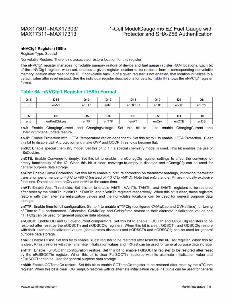
nNVCfg1 Register (1B9h) Register Type: Special Nonvolatile Restore: There is no associated restore location for this register. The nNVCfg1 register manages nonvolatile memory restore of device and fuel gauge register RAM locations. Each bit of the nNVCfg1 register, when set, enables a given register location to be restored from a corresponding nonvolatile memory location after reset of the IC. If nonvolatile backup of a given register is not enabled, that location initializes to a default value after reset instead. See the individual register descriptions for details. Table 64 shows the nNVCfg1 register format.
Table 64. nNVCfg1 Register (1B9h) Format D15 D14 D13 D12 D11 D10 D9 D8
0 enMtl enFTh enRF enODSC enJP enSC enProt
D7 D6 D5 D4 D3 D2 D1 D0 enJ enProtChksm enTP enTTF enAT enCrv enCTE enDS
enJ: Enable ChargingCurrent and ChargingVoltage. Set this bit to 1 to enable ChargingCurrent and ChargingVoltage update feature. enJP: Enable Protection with JIETA (temperature region dependent). Set this bit to 1 to enable JIETA Protection. Clear this bit to disable JEITA protection and make OVP and OCCP thresholds become flat. enSC: Enable special chemistry model. Set this bit to 1 if a special chemistry model is used. This bit enables the use of nScOcvLim. enCTE: Enable Converge-to-Empty. Set this bit to enable the nConvgCfg register settings to affect the converge-to-empty functionality of the IC. When this bit is clear, converge-to-empty is disabled and nConvgCfg can be used for general purpose data storage. enCrv: Enable Curve Correction. Set this bit to enable curvature correction on thermistor readings, improving thermistor translation performance to -40°C to +80°C (instead of -10°C to +50°C). Note that enCrv and enMtl are mutually exclusive functions. Do not set both enCrv and enMtl at the same time. enAT: Enable Alert Thresholds. Set this bit to enable IAlrtTh, VAlrtTh, TAlrtTh, and SAlrtTh registers to be restored after reset by the nIAlrtTh, nVAlrtTh, nTAlrtTh, and nSAlrtTh registers respectively. When this bit is clear, these registers restore with their alternate initialization values and the nonvolatile locations can be used for general purpose data storage. enTTF: Enable time-to-full configuration. Set to 1 to enable nTTFCfg (configures CVMixCap and CVHalftime) for tuning of Time-to-Full performance. Otherwise, CVMixCap and CVHalftime restore to their alternate initialization values and nTTFCfg can be used for general purpose data storage. enODSC: Enable OD and SC over-current comparators. Set this bit to enable ODSCTh and ODSCCfg registers to be restored after reset by the nODSCTh and nODSCCfg registers. When this bit is clear, ODSCTh and ODSCCfg restore with their alternate initialization values (comparators disabled) and nODSCTh and nODSCCfg can be used for general purpose data storage. enRF: Enable RFast. Set this bit to enable RFast register to be restored after reset by the nRFast register. When this bit is clear, RFast restores with their alternate initialization values and nRFast can be used for general purpose data storage. enFTh: Enable FullSOCThr configuration restore. Set this bit to enable FullSOCThr register to be restored after reset by the nFullSOCThr register. When this bit is clear, FullSOCThr restores with its alternate initialization value and nFullSOCThr can be used for general purpose data storage. enMtl: Enable CGTempCo restore. Set this bit to enable CGTempCo register to be restored after reset by the nTCurve register. When this bit is clear, CGTempCo restores with its alternate initialization value. nTCurve can be used for general
MAX17301–MAX17303/MAX17311–MAX17313
1-Cell ModelGauge m5 EZ Fuel Gauge withProtector and SHA-256 Authentication
www.maximintegrated.com Maxim Integrated | 91

purpose data storage if both enCrv and enMtl are clear. Do not set both enCrv and enMtl at the same time. enTP: Set to 1 to associate the TaskPeriod register with nTaskPeriod MTP. Otherwise, TaskPeriod restores with the POR value and the register’s address configures nRippleCfg instead of nTaskPeriod. enDS: Set to 0. Don't set to 1. enProt: Enable Protector. Set this bit to enable the protector. When this bit is clear, protector is disabled. enProtChksm: Enable protector checksum function. Set this bit to enable the protector checksum function. When this bit is clear, the checksum protection is disabled. 0: This location must remain 0. Do not write this location to 1.
nNVCfg2 Register (1BAh) Register Type: Special Nonvolatile Restore: There is no associated restore location for this register. The nNVCfg2 register manages nonvolatile memory backup and restore of device and fuel gauge register RAM locations. Each bit of the nNVCfg2 register, when set, enables a given register location to be restored from or backed up to a corresponding nonvolatile memory location after reset of the IC. If nonvolatile backup of a given register is not enabled, that location initializes to a default value after reset instead. See the individual register descriptions for details. Table 65 shows the nNVCfg2 register format.
Table 65. nNVCfg2 Register (1BAh) Format D15 D14 D13 D12 D11 D10 D9 D8 D7 D6 D5 D4 D3 D2 D1 D0 enT 0 enMMT enMMV enMMC enVT enFC enMet FibMax FibScl
FibMax/FibScl. Set the FibMax and FibScl "Fibonacci Saving" interval to provide recurring log-saving according to the expected battery lifespan. See the 100 Record Life Logging section for more details. enMet: Enable metal current sensing. Setting this bit to 1 enables temperature compensation of current readings for allowing copper trace current sensing. This also forces the PackCfg.TdEn bit to 1 after reset of the IC to guarantee internal temperature measurements occurs. See nNVCfg1.enMtl, which enables nTCurve register operation for adjustment of the current sensing temperature coefficient. enFC: Enable FullCap and FullCapRep backup and restore. Set this bit to enable FullCap and FullCapRep registers to be restored after reset by the nFullCapRep register and FullCapRep to backup to nFullCapRep. When this bit is clear, FullCap and FullCapRep registers restore from the nFullCapNom register. nFullCapRep can then be used as general purpose user memory. enVT: Enable Voltage and Temperature backup. Set this bit to enable storage of AvgVCell and AvgTA register information into the nVoltTemp register during save operations. There is no corresponding restore option. When this bit and nNVCfg0.enAF are clear, nVoltTemp can be used as general purpose memory. Note that enVT should not be set simultaneously with nNVCfg0.enAF (AgeForecasting). enMMC: Enable MinMaxCurr Backup. Set this bit to enable storage of MinMaxCurr register information into the nMinMaxCurr register during save operations. There is no corresponding restore option. When this bit is clear, nMinMaxCurr can be used as general purpose memory. enMMV: Enable MinMaxVolt Backup. Set this bit to enable storage of MinMaxVolt register information into the nMinMaxVolt register during save operations. There is no corresponding restore option. When this bit is clear, nMinMaxVolt can be used as general purpose memory. enMMT: Enable MinMaxTemp Backup. Set this bit to enable storage of MinMaxTemp register information into the nMinMaxTemp register during save operations. There is no corresponding restore option. When this bit is clear, nMinMaxTemp can be used as general purpose memory.
MAX17301–MAX17303/MAX17311–MAX17313
1-Cell ModelGauge m5 EZ Fuel Gauge withProtector and SHA-256 Authentication
www.maximintegrated.com Maxim Integrated | 92

enT: Enable TimerH backup and restore. Set this bit to enable TimerH register to be backed up and restored by the nTimerH register. When this bit is clear, TimerH restores with its alternate initialization value and nTimerH can be used as general purpose memory.
Enabling and Freeing Nonvolatile vs. Defaults There are seven nonvolatile memory words labeled nUser that are dedicated to general purpose user data storage. Most other nonvolatile memory locations can also be used as general purpose storage if their normal function is disabled. The nNVCfg0, nNVCfg1, and nNVCfg2 registers control which nonvolatile memory functions are enabled and disabled. Table 66 shows how to free up the specific registers for user data storage. Table 67 shows which nNVCfg bits control different IC functions and the effects when the bit is set or cleared. See the nNVCfg register descriptions for complete details. Do not convert a nonvolatile register to general purpose memory space if that register's function is used by the application. Below is a summary of how many bytes can be made available for user memory and the functional trade off to free up those bytes. 156 bytes maximum freeable: The cost is to sacrifice any optional features/configuration, including no custom OCV
table and protector disabled. 74 bytes reasonably freeable: Made available without reverting halfway to EZ or disabling protector. 62 bytes freeable: Made available by using half of miscellaneous configurability. 42 bytes easily freeable 34 bytes always free: If SBS mode is not enabled. 4 bytes always free: If SBS enabled is enabled.
Table 66. Making Nonvolatile Memory Available for User Data RELATED
FEATURE FREE BY: BYTES REGISTERS ADDRESS COMMENTS
MAJOR FEATURE CHOICES
Always Free Always 1 word 2 bytes “Reserved” 0x1E4
SBS NVM
Disable SBS and DS2438 features nNVCfg0.enSBS = 0 nNVCfg1.enDS = 0
15 words 30 bytes
nSBSCfg nManfctrName[0:2] nDesignVoltage nManfctrDate nFirstUsed nSerialNumber[0:2] nDeviceName[0:4]
0x1B4, 0x1CC-0x1CE, 0x1E3, 0x1E8-0x1EF
Generally freeable
Time-to-Full Configurability
nNVCfg1.enTTF = 0
1 word 2 bytes nTTFCfg 0x1C7
Free if default nTTFCfg is acceptable.
Dynamic Power nNVCfg0.enDP = 0 1 word
2 bytes nDPLimit 0x1E0 Free if feature is not used.
Age Forecasting nNVCfg0.enAF = 0 1 word
2 bytes nAgeFcCfg 0x1E2
Free if feature is not used. Has additional implications with nVoltTemp.
LiFePO4 nNVCfg1.enSC 1 word 2 bytes nScOcvLim 0x1E1 Free if feature is not
used.
JEITA Charge Voltage/Current vs. Temp
nNVCfg0.enJ = 0 nNVCfg0.enJP = 0
2 words 4 bytes
nJEITAC nStepChg
0x1D8 0x1DB
Free if feature is not used. Note that nJEITAV and nJEITACfg are still required for protector
MAX17301–MAX17303/MAX17311–MAX17313
1-Cell ModelGauge m5 EZ Fuel Gauge withProtector and SHA-256 Authentication
www.maximintegrated.com Maxim Integrated | 93
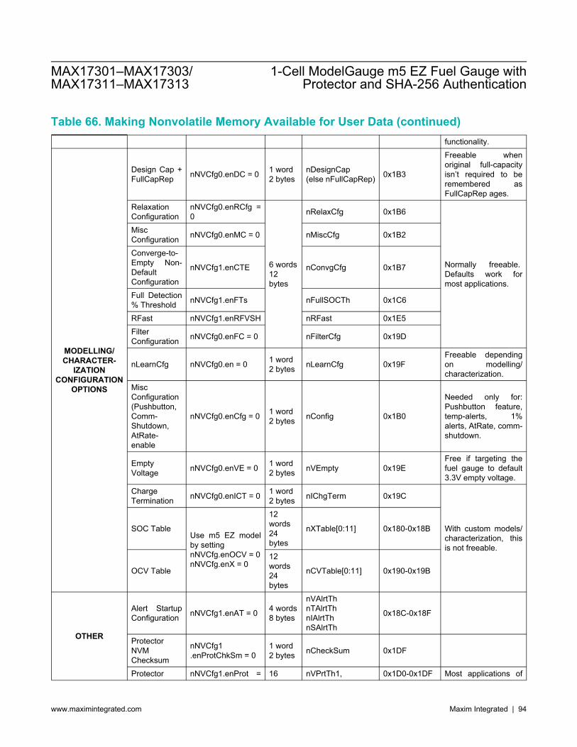
Table 66. Making Nonvolatile Memory Available for User Data (continued) functionality.
MODELLING/ CHARACTER-
IZATION CONFIGURATION
OPTIONS
Design Cap + FullCapRep nNVCfg0.enDC = 0 1 word
2 bytes nDesignCap (else nFullCapRep) 0x1B3
Freeable when original full-capacity isn’t required to be remembered as FullCapRep ages.
Relaxation Configuration
nNVCfg0.enRCfg = 0
6 words 12 bytes
nRelaxCfg 0x1B6
Normally freeable. Defaults work for most applications.
Misc Configuration nNVCfg0.enMC = 0 nMiscCfg 0x1B2
Converge-to-Empty Non-Default Configuration
nNVCfg1.enCTE nConvgCfg 0x1B7
Full Detection % Threshold nNVCfg1.enFTs nFullSOCTh 0x1C6
RFast nNVCfg1.enRFVSH nRFast 0x1E5 Filter Configuration nNVCfg0.enFC = 0 nFilterCfg 0x19D
nLearnCfg nNVCfg0.en = 0 1 word 2 bytes nLearnCfg 0x19F
Freeable depending on modelling/characterization.
Misc Configuration (Pushbutton, Comm-Shutdown, AtRate-enable
nNVCfg0.enCfg = 0 1 word 2 bytes nConfig 0x1B0
Needed only for: Pushbutton feature, temp-alerts, 1% alerts, AtRate, comm-shutdown.
Empty Voltage nNVCfg0.enVE = 0 1 word
2 bytes nVEmpty 0x19E Free if targeting the fuel gauge to default 3.3V empty voltage.
Charge Termination nNVCfg0.enICT = 0 1 word
2 bytes nIChgTerm 0x19C
With custom models/characterization, this is not freeable.
SOC Table Use m5 EZ model by setting nNVCfg.enOCV = 0 nNVCfg.enX = 0
12 words 24 bytes
nXTable[0:11] 0x180-0x18B
OCV Table
12 words 24 bytes
nCVTable[0:11] 0x190-0x19B
OTHER
Alert Startup Configuration nNVCfg1.enAT = 0 4 words
8 bytes
nVAlrtTh nTAlrtTh nIAlrtTh nSAlrtTh
0x18C-0x18F
Protector NVM Checksum
nNVCfg1 .enProtChkSm = 0
1 word 2 bytes nCheckSum 0x1DF
Protector nNVCfg1.enProt = 16 nVPrtTh1, 0x1D0-0x1DF Most applications of
MAX17301–MAX17303/MAX17311–MAX17313
1-Cell ModelGauge m5 EZ Fuel Gauge withProtector and SHA-256 Authentication
www.maximintegrated.com Maxim Integrated | 94

Table 66. Making Nonvolatile Memory Available for User Data (continued)
0 nNVCfg1.enJP = 0
words 32 bytes
nTPrtTh1 nTPrtTh3, nIPrtTh1 nVPrtTh2, nTPrtTh2 nProtMisTh nProtCfg, nJEITAV nJEITACfg, nDelayCfg nODSCTh, nODSCCfg nCheckSum (below if JEITA also off) nJEITAC, nStepChg
MAX1730x/MAX1731x use protector. However, if the protector is entirely disabled, these 32 bytes become free NVM. FET drivers and protection do not execute in this configuration.
Table 67. Nonvolatile Memory Configuration Options
ADDRESS REGISTER NAME
FACTORY DEFAULT
CONTROL BIT(S)
FUNCTION WHEN CONTROL BIT IS SET
FUNCTION WHEN CONTROL BIT(S)
CLEARED
180h - 18Bh
nXTable0 through
nXTable12 All 0x0000 nNVCfg0.enX 180h-18Bh Hold Custom
Cell Model Information
Becomes Free1, IC Uses Default EZ
Cell Model 18Ch nVAlrtTh 0x0000
nNVCfg1.enAT
VAlrtTh, TAlrtTh, IAlrtTh, SAlrtTh
initialize from nVAlrtTh, nTAlrtTh, nIAlrtTh,
nSAlrtTh
Becomes Free1, VAlrtTh, TAlrtTh, IAlrtTh, SAlrtTh
→ Disabled Threshold Values
18Dh nTAlrtTh 0x0000 18Eh nIAlrtTh 0x0000 18Fh nSAlrtTh 0x0000
190h - 19Bh
nOCVTable0 through
nOCVTable12 All 0x0000 nNVCfg0.enOCV 190h-19Bh Hold Custom
Cell Model Information
Becomes Free1, IC Uses Default EZ
Cell Model
19Ch nIChgTerm 0x0000 nNVCfg0.enICT nIChgTerm→ IChgTerm Becomes Free1,
IChgTerm = FullCapRep/3
19Dh nFilterCfg 0x0000 nNVCfg0.enFCfg nFilterCfg→ FilterCfg Becomes Free1, FilterCfg = 0x0EA4
19Eh nVEmpty 0x0000 nNVCfg0.enVE nVEmpty→ VEmpty Becomes Free1, VEmpty = 0xA561
19Fh nLearnCfg 0x0000 nNVCfg0.enLCfg nLearnCfg → LearnCfg Becomes Free1, LearnCfg = 0x2687
1A0h nQRTable00 0x1080
N/A
Always QRTable Information nQRTable00→ QRTable00 nQRTable10→ QRTable10 nQRTable20→ QRTable20
1A1h nQRTable10 0x2043
1A2h nQRTable20 0x078C 1A3h nQRTable30 0x0880
MAX17301–MAX17303/MAX17311–MAX17313
1-Cell ModelGauge m5 EZ Fuel Gauge withProtector and SHA-256 Authentication
www.maximintegrated.com Maxim Integrated | 95

Table 67. Nonvolatile Memory Configuration Options (continued)
ADDRESS REGISTER NAME
FACTORY DEFAULT
CONTROL BIT(S)
FUNCTION WHEN CONTROL BIT IS SET
FUNCTION WHEN CONTROL BIT(S)
CLEARED
nQRTable30→ QRTable30
1A4h nCycles 0x0000 Always nCycles→ Cycles 1A5h nFullCapNom 0x0BB8 Always nFullCapNom→ FullCapNom 1A6h nRComp0 0x08CC Always nRComp0→ RComp0 1A7h nTempCo 0x223E Always nTempCo→ TempCo
1A8h nBattStatus 0x0000 nNVCfg1.enProt nProtCfg.PFen
Logs/Saves Permanent Failure Status Becomes Free1
1A9h nFullCapRep 0x1A90 nNVCfg2.enFC nFullCapRep→ FullCapRep
Becomes Free1
nFullCapNom→ FullCapRep
1AAh nVoltTemp 0x0000
nNVCfg2.enVT (nNVCfg0.enAF
= 0)
AvgVCell→ nVoltTemp and AvgTA→ nVoltTemp
at each backup event
Becomes Free1, Voltage, Temperature
Logging Disabled
nNVCfg0.enAF (nNVCfg2.enVT
= 0)
nVoltTemp stores Age Forecasting Information
Becomes Free1, Age Forecasting
Disabled
1ABh nMaxMinCurr 0x807F nNVCfg2.enMMC MaxMinCurr→
nMaxMinCurr at each backup event
Becomes Free1
1ACh nMaxMinVolt 0x00FF nNVCfg2.enMMV MaxMinVolt→
nMaxMinVolt at each backup event
Becomes Free1,
1ADh nMaxMinTemp 0x807F nNVCfg2.enMMT MaxMinTemp→
nMaxMinTemp at each backup event
Becomes Free1,
1AEh nFullCapFlt 0x0000 nNVCfg0.enAF nFullCapFlt stores Age
Forecasting backup information
Becomes Free1, Age Forecasting
Disabled
1AFh nTimerH 0x0000 nNVCfg2.enT TimerH→ nTimerH at each backup event Becomes Free1,
1B0h nConfig 0x0000 nNVCfg0.enCfg nConfig→ Config
nConfig→ Config2
Becomes Free1, Config =
0x2214, Config2 = 0x2058
1B1h nRippleCfg 0x0204 N/A Always nRippleCfg→ RippleCfg
1B2h nMiscCfg 0x0000 nNVCfg0.enMC nMiscCfg→ MiscCfg Becomes Free1,
MAX17301–MAX17303/MAX17311–MAX17313
1-Cell ModelGauge m5 EZ Fuel Gauge withProtector and SHA-256 Authentication
www.maximintegrated.com Maxim Integrated | 96
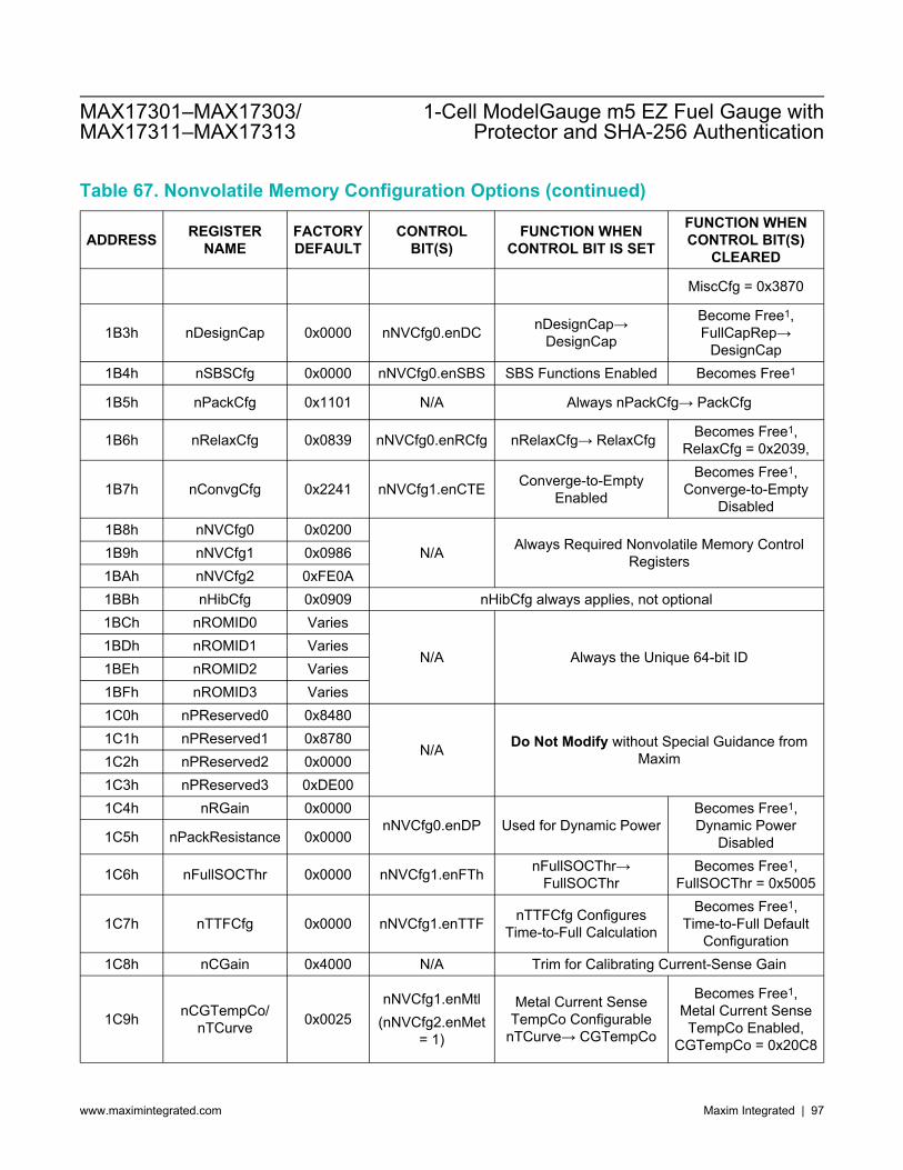
Table 67. Nonvolatile Memory Configuration Options (continued)
ADDRESS REGISTER NAME
FACTORY DEFAULT
CONTROL BIT(S)
FUNCTION WHEN CONTROL BIT IS SET
FUNCTION WHEN CONTROL BIT(S)
CLEARED
MiscCfg = 0x3870
1B3h nDesignCap 0x0000 nNVCfg0.enDC nDesignCap→ DesignCap
Become Free1, FullCapRep→
DesignCap 1B4h nSBSCfg 0x0000 nNVCfg0.enSBS SBS Functions Enabled Becomes Free1
1B5h nPackCfg 0x1101 N/A Always nPackCfg→ PackCfg
1B6h nRelaxCfg 0x0839 nNVCfg0.enRCfg nRelaxCfg→ RelaxCfg Becomes Free1, RelaxCfg = 0x2039,
1B7h nConvgCfg 0x2241 nNVCfg1.enCTE Converge-to-Empty Enabled
Becomes Free1, Converge-to-Empty
Disabled 1B8h nNVCfg0 0x0200
N/A Always Required Nonvolatile Memory Control Registers 1B9h nNVCfg1 0x0986
1BAh nNVCfg2 0xFE0A 1BBh nHibCfg 0x0909 nHibCfg always applies, not optional 1BCh nROMID0 Varies
N/A Always the Unique 64-bit ID 1BDh nROMID1 Varies 1BEh nROMID2 Varies 1BFh nROMID3 Varies 1C0h nPReserved0 0x8480
N/A Do Not Modify without Special Guidance from Maxim
1C1h nPReserved1 0x8780 1C2h nPReserved2 0x0000 1C3h nPReserved3 0xDE00 1C4h nRGain 0x0000
nNVCfg0.enDP Used for Dynamic Power Becomes Free1, Dynamic Power
Disabled 1C5h nPackResistance 0x0000
1C6h nFullSOCThr 0x0000 nNVCfg1.enFTh nFullSOCThr→ FullSOCThr
Becomes Free1, FullSOCThr = 0x5005
1C7h nTTFCfg 0x0000 nNVCfg1.enTTF nTTFCfg Configures Time-to-Full Calculation
Becomes Free1, Time-to-Full Default
Configuration 1C8h nCGain 0x4000 N/A Trim for Calibrating Current-Sense Gain
1C9h nCGTempCo/ nTCurve 0x0025
nNVCfg1.enMtl (nNVCfg2.enMet
= 1)
Metal Current Sense TempCo Configurable
nTCurve→ CGTempCo
Becomes Free1, Metal Current Sense
TempCo Enabled, CGTempCo = 0x20C8
MAX17301–MAX17303/MAX17311–MAX17313
1-Cell ModelGauge m5 EZ Fuel Gauge withProtector and SHA-256 Authentication
www.maximintegrated.com Maxim Integrated | 97

Table 67. Nonvolatile Memory Configuration Options (continued)
ADDRESS REGISTER NAME
FACTORY DEFAULT
CONTROL BIT(S)
FUNCTION WHEN CONTROL BIT IS SET
FUNCTION WHEN CONTROL BIT(S)
CLEARED
(nNVCfg1.enCrv = 0)
nNVCfg1.enCrv (nNVCfg2.enMet
= 0) (default)
Thermistor Curvature Controlled by nTCurve
Becomes Free1, Thermistor Curvature
Disabled
1CAh nTGain 0xEE56 N/A Configuration for Translating Thermistor to ºC
1CBh nTOff 0x1DA4 1CCh nManfctrName0 0x0000
nNVCfg0.enSBS nManfctrName[2:0]→ sManfctrName Becomes Free1 1CDh nManfctrName1 0x0000
1CEh nManfctrName2 0x0000
1CFh nRSense 0x03E8 N/A Sense Resistor Value—Helps Host Translate Currents and Capacities
1D0h nVPrtTh1 0x508C
nNVCfg1.enProt Configures Protection Thresholds
Becomes Free1
Protector Disabled
1D1h nTPrtTh1 0x3700 1D2h nTPrtTh3 0x5528 1D3h nIPrtTh1 0x4BB5 1D4h nVPrtTh2 0xDC00 1D5h nTPrtTh2 0x2D0A 1D6h nProtMiscTh 0x7A28 1D7h nProtCfg 0x0A00 1D8h nJEITAC 0x644B 1D9h nJEITAV 0x0059 1DAh nJeitaCfg 0x5054 1DBh nStepChg 0xC884 1DCh nDelayCfg 0xAB3D 1DDh nODSCTh 0x0EAF 1DEh nODSCCfg 0x4345
1DFh nCheckSum 0x0017 nNVCfg1.
enProtChkSm and enProt
Holds CheckSum Value of 0x1A0-0x1AE for Validating NVM at
Startup
Becomes Free1
1E0h nDPLimit 0x0000 nNVCfg0.enDP Configures Dynamic Power
Becomes Free1
Dynamic Power Disabled
MAX17301–MAX17303/MAX17311–MAX17313
1-Cell ModelGauge m5 EZ Fuel Gauge withProtector and SHA-256 Authentication
www.maximintegrated.com Maxim Integrated | 98

Table 67. Nonvolatile Memory Configuration Options (continued)
ADDRESS REGISTER NAME
FACTORY DEFAULT
CONTROL BIT(S)
FUNCTION WHEN CONTROL BIT IS SET
FUNCTION WHEN CONTROL BIT(S)
CLEARED
1E1h nScOcvLim 0x0000 nNVCfg1.enSC Used for LiFePO4 Gauging
Becomes Free1
LiFePO4 Disabled 1E2h nAgeFcCfg 0x0000 nNVCfg0.enAF Configures Age Forecast Becomes Free1
1E3h nDesignVoltage 0x0000 nNVCfg0.enSBS nDesignVoltage→ sDesignVolt Becomes Free1
1E4h Reserved 0x0000 N/A Reserved
1E5h nRFast 0x0000 nNVCfg1.enRF nRFast→ RFast Becomes Free1,
RFast = 0x0500
1E6h nManfctrDate 0x0000
nNVCfg0.enSBS
nManfctrDate→ sManfctrDate Becomes Free1
1E7h nFirstUsed 0x0000 nFirstUsed→ sFirstUsed Becomes Free1
1E8h nSerialNumber0 0x0000 nSerialNumber[2:0]→
sSerialNumber Becomes Free1 1E9h nSerialNumber1 0x0000 1EAh nSerialNumber2 0x0000 1EBh nDeviceName0 0x0000
nDeviceName[4:0]→ sDeviceName Becomes Free1
1ECh nDeviceName1 0x0000 1EDh nDeviceName2 0x0000 1EEh nDeviceName3 0x0000 1EFh nDeviceName4 0x0000
Note 1: "Free" indicates the address is unused and available as general user nonvolatile.
Shadow RAM Nonvolatile memory is never written to or read from directly by the communication interface. Instead, data is written to or read from shadow RAM memory located at the same address. Copy and recall commands are used to transfer data between the nonvolatile memory and the shadow RAM. Figure 24 describes this relationship. Nonvolatile memory recall occurs automatically at IC power-up and software POR.
MAX17301–MAX17303/MAX17311–MAX17313
1-Cell ModelGauge m5 EZ Fuel Gauge withProtector and SHA-256 Authentication
www.maximintegrated.com Maxim Integrated | 99

Shadow RAM and Nonvolatile Memory Relationship
0180h
SHADOW RAM
0180h
NON-VOLATILE MEMORY
DATA WRITE
DATA READ
CO
MM
UN
ICAT
ION
INTE
RFA
CE
COPY NV BLOCK
NV RECALL
01EFh 01EFh
Figure 24. Shadow RAM and Nonvolatile Memory Relationship
Nonvolatile Memory Commands The following commands are used to copy or recall data from the nonvolatile memory. All commands are written to the Command register at memory address 060h to perform the desired operation. The CommStat register can be used to track the status of the request.
COPY NV BLOCK [E904h] This command copies the entire block from shadow RAM to nonvolatile memory addresses 180h to 1DFh excluding the unique ID locations of 1BCh to 1BFh. After issuing this command, the host must wait tBLOCK for the operation to complete. The configuration memory can be copied a maximum of seven times. Note that the supply voltage must be above VNVM for the operation to complete successfully.
NV RECALL [E001h] This command recalls the entire block from nonvolatile memory to Shadow RAM addresses 180h to 1DFh. This is a low power operation that takes up to tRECALL to complete. Note that the supply voltage must be above VNVM for the operation to complete successfully.
HISTORY RECALL [E2XXh] This command copies history data into page 1Fh of memory. After issuing this command, the host must wait tRECALL for the operation to complete before reading page 1Fh. Table 68 shows what history information can be recalled. See SHA-256, Battery Life Logging, and Determining Number of Remaining Updates sections for details on how to decode this information.
Table 68. History Recall Command Functions COMMAND FUNCTION
0xE29D Recall indicator flags to determine remaining SHA-256 secret updates or clears 0xE29B Recall indicator flags to determine remaining configuration memory writes
MAX17301–MAX17303/MAX17311–MAX17313
1-Cell ModelGauge m5 EZ Fuel Gauge withProtector and SHA-256 Authentication
www.maximintegrated.com Maxim Integrated | 100

Table 68. History Recall Command Functions (continued) COMMAND FUNCTION
0xE29C Recall indicator flags to determine remaining Battery Life Logging updates 0xE29C, 0xE29D Recall indicator flags to determine Battery Life Logging update errors 0xE22E to 0xE291 Recall Battery Life Logging information
Nonvolatile Block Programming The host must program all nonvolatile memory locations at the same time by using the Copy NV Block command. The host first writes all desired nonvolatile memory Shadow RAM locations to their desired values, then sends the Copy NV Block command, and then waits tBLOCK for the copy to complete. Afterwards, the host should send the power-on-reset sequence to reset the IC and have the new nonvolatile settings take effect. The CommStat.NVError bit should be read to determine if the copy command executed successfully. Note that configuration memory is limited to nBLOCK total write attempts. The recommended full sequence is: 1. Write desired memory locations to new values. 2. Clear CommStat.NVError bit. 3. Write 0xE904 to the Command register 0x060 to initiate a block copy. 4. Wait tBLOCK for the copy to complete. 5. Check the CommStat.NVError bit. If set, repeat the process. If clear, continue. 6. Write 0x000F to the Command register 0x060 to POR the IC. 7. Wait 10ms for the IC to reset. 8. Write 0x8000 to Config2 register 0x0AB to reset firmware. 9. Wait for POR_CMD bit (bit 15) of the Config2 register to be cleared to indicated POR sequence is complete.
Determining Number of Remaining Updates The configuration memory can only be updated seven times by the user (first update occurs during manufacturing test). The number of remaining updates can be calculated using the following procedure: 1. Write 0xE29B to the Command register (060h). 2. Wait tRECALL. 3. Read memory address 1FDh. 4. Decode address 1FDh data as shown in Table 69. Each block write has redundant indicator flags for reliability. Logically OR the upper and lower bytes together then count the number of 1s determine how many updates have already been used. The first update occurs in manufacturing test prior to shipping to the user.
Table 69. Number of Remaining Config Memory Updates ADDRESS 1FDH
DATA LOGICAL OR OF UPPER AND LOWER
BYTES NUMBER OF UPDATES
USED NUMBER OF UPDATES
REMAINING
0000000x00000001b or 000000010000000xb
00000001b 1 7
000000xx0000001xb 00000011b 2 6
MAX17301–MAX17303/MAX17311–MAX17313
1-Cell ModelGauge m5 EZ Fuel Gauge withProtector and SHA-256 Authentication
www.maximintegrated.com Maxim Integrated | 101

Table 69. Number of Remaining Config Memory Updates (continued) ADDRESS 1FDH
DATA LOGICAL OR OF UPPER AND LOWER
BYTES NUMBER OF UPDATES
USED NUMBER OF UPDATES
REMAINING
or 0000001x000000xxb
00000xxx000001xxb or 000001xx00000xxxb
00000111b 3 5
0000xxxx00001xxxb or 00001xxx0000xxxxb
00001111b 4 4
000xxxxx0001xxxxb or 0001xxxx000xxxxxb
00011111b 5 3
00xxxxxx001xxxxxb or 001xxxxx00xxxxxxb
00111111b 6 2
0xxxxxxx01xxxxxxb or 01xxxxxx0xxxxxxxb
01111111b 7 1
xxxxxxxx1xxxxxxxb or 1xxxxxxxxxxxxxxxb
11111111b 8 0
nLearnCfg Register (19Fh) Register Type: Special Nonvolatile Restore: LearnCfg (0A1h) if nNVCfg0.enLCfg is set. Alternate Initial Value: 0x2687 The nLearnCfg register controls all functions relating to adaptation during operation. Table 70 shows the register format.
Table 70. LearnCfg (0A1h)/nLearnCfg (19Fh) Register Format D15 D14 D13 D12 D11 D10 D9 D8 D7 D6 D5 D4 D3 D2 D1 D0
0 1 0 0 0 1 1 0 1 LS 0 1 1 1
0: Bit must be written 0. Do not write 1. 1: Bit must be written 1. Do not write 0. LS: Learn Stage. The Learn Stage value controls the influence of the voltage fuel gauge on the mixing algorithm. Learn Stage defaults to 0h, making the voltage fuel gauge dominate. Learn Stage then advances to 7h over the course of two
MAX17301–MAX17303/MAX17311–MAX17313
1-Cell ModelGauge m5 EZ Fuel Gauge withProtector and SHA-256 Authentication
www.maximintegrated.com Maxim Integrated | 102

full cell cycles to make the coulomb counter dominate. Host software can write the Learn Stage value to 7h to advance to the final stage at any time. Writing any value between 1h and 6h is ignored.
nMiscCfg Register (1B2h) Register Type: Special Nonvolatile Restore: MiscCfg (00Fh) if nNVCfg0.enMC is set. Alternate Initial Value: 0x3070 The nMiscCfg control register enables various other functions of the device. The nMiscCfg register default values should not be changed unless specifically required by the application. Table 71 shows the register format.
Table 71. MiscCfg (00Fh)/nMiscCfg (1B2h) Register Format D15 D14 D13 D12 D11 D10 D9 D8 D7 D6 D5 D4 D3 D2 D1 D0
FUS 0 0 MR 1 0 0 SACFG
0: Bit must be written 0. Do not write 1. 1: Bit must be written 1. Do not write 0. SACFG: SOC Alert Config. SOC Alerts can be generated by monitoring any of the SOC registers as follows. SACFG defaults to 00 at power-up: 0 0 SOC Alerts are generated based on the RepSOC register. 0 1 SOC Alerts are generated based on the AvSOC register. 1 0 SOC Alerts are generated based on the MixSOC register. 1 1 SOC Alerts are generated based on the VFSOC register. MR: Mixing Rate. This value sets the strength of the servo mixing rate after the final mixing state has been reached (> 2.08 complete cycles). The units are MR0 = 6.25μV, giving a range up to 19.375mA with a standard 0.010Ω sense resistor. Setting this value to 00000b disables servo mixing and the IC continues with time-constant mixing indefinitely. The default setting is 18.75μV or 1.875mA with a standard sense resistor. FUS: Full Update Slope. This field prevents jumps in the RepSOC and FullCapRep registers by setting the rate of adjustment of FullCapRep near the end of a charge cycle. The update slope adjustment range is from 2% per 15 minutes (0000b) to a maximum of 32% per 15 minutes (1111b).
nConfig Register (1B0h) Register Type: Special Nonvolatile Restore: Config (00Bh) and Config2 (0ABh) if nNVCfg0.enCfg is set. Alternate Initial Value: 0x2214 for Config, 0x0050 for Config2 The nConfig register holds all shutdown enable, alert enable, and temperature enable control bits. Writing a bit location enables the corresponding function within one task period. Table 72, Table 73, and Table 74 show the register formats.
Table 72. nConfig Register (1B0h) Format D15 D14 D13 D12 D11 D10 D9 D8 D7 D6 D5 D4 D3 D2 D1 D0
0 SS TS VS 0 PBen 1 0 AtRateEn COMMSH FastADCen 1 FTHRM Aen dSOCen TAlrtEn
MAX17301–MAX17303/MAX17311–MAX17313
1-Cell ModelGauge m5 EZ Fuel Gauge withProtector and SHA-256 Authentication
www.maximintegrated.com Maxim Integrated | 103

Table 73. Config Register (00Bh) Format D15 D14 D13 D12 D11 D10 D9 D8 D7 D6 D5 D4 D3 D2 D1 D0
0 SS TS VS 0 PBen 1 0 SHDN COMMSH FastADCen ETHRM FTHRM Aen Bei Ber
Table 74. Config2 Register (0ABh) Format D15 D14 D13 D12 D11 D10 D9 D8 D7 D6 D5 D4 D3 D2 D1 D0
POR_CMD 0 AtRtEn 0 0 0 0 0 dSOCen TAlrtEn 0 1 DRCfg CPMode 0
0: Bit must be written 0. Do not write 1. 1: Bit must be written 1. Do not write 0. PBEn: PushButton enable. Set PBEn = 1 to enable wakeup by pushbutton. This application allows a gadget to be completely sealed with battery disconnected until a shared system button is pressed. Ber: Enable alert on battery removal when the IC is mounted host side. When Ber = 1, a battery-removal condition, as detected by the TH pin voltage, triggers an alert. Note that if this bit is set to 1, the ALSH bit should be set to 0 to prevent an alert condition from causing the device to enter shutdown mode. Bei: Enable alert on battery insertion when the IC is mounted host side. When Bei = 1, a battery-insertion condition, as detected by the TH pin voltage, triggers an alert. Note that if this bit is set to 1, the ALSH bit should be set to 0 to prevent an alert condition from causing the device to enter shutdown mode. Aen: Enable alert on fuel-gauge outputs. When Aen = 1, violation of any of the alert threshold register values by temperature, voltage, or SOC triggers an alert. This bit affects the ALRT1 pin operation only. The Smx, Smn, Tmx, Tmn, Vmx, Vmn, Imx, and Imn bits of the Status register (000h) are not disabled. Note that if this bit is set to 1, the ALSH bit should be set to 0 to prevent an alert condition from causing the device to enter shutdown mode. FTHRM: Force Thermistor Bias Switch. This allows the host to control the bias of the thermistor switch or enable fast detection of battery removal. Set FTHRM = 1 to always enable the thermistor bias switch. With a standard 10kΩ thermistor, this adds an additional ~200μA to the current drain of the circuit. ETHRM: Enable Thermistor. Set to logic 1 to enable the automatic TH output bias and TH measurement. FastADCen: Enable FastADC. Set to logic 1 to enable the FastADC feature. COMMSH: Communication Shutdown. Set to logic 1 to force the device to enter shutdown mode if both SDA and SCL are held low (MAX17301-MAX17303) or DQ is held low (MAX17311-MAX17313) for more than timeout of the ShdnTimer register. This also configures the device to wake up on a rising edge of any communication. Note that if COMMSH and AINSH are both set to 0, the device wakes up an edge of any of the DQ/SDA or OD/SCL pins. See Table 6. SHDN: Shutdown. Write this bit to logic 1 to force a shutdown of the device after timeout of the ShdnTimer register (default 45s delay). SHDN is reset to 0 at power-up and upon exiting shutdown mode. In order to command shutdown within 45 seconds, first write HibCFG = 0x0000 to enter active mode. VS: Voltage ALRT1 Sticky. When VS = 1, voltage alerts can only be cleared through software. When VS = 0, voltage alerts are cleared automatically when the threshold is no longer exceeded. TS: Temperature ALRT1 Sticky. When TS = 1, temperature alerts can only be cleared through software. When TS = 0, temperature alerts are cleared automatically when the threshold is no longer exceeded. SS: SOC ALRT1 Sticky. When SS = 1, SOC alerts can only be cleared through software. When SS = 0, SOC alerts are cleared automatically when the threshold is no longer exceeded. POR_CMD: Firmware Restart. Set this bit to 1 to restart IC firmware operation without performing a recall of nonvolatile memory into RAM. This allows different IC configurations to be tested without changing nonvolatile memory settings. This
MAX17301–MAX17303/MAX17311–MAX17313
1-Cell ModelGauge m5 EZ Fuel Gauge withProtector and SHA-256 Authentication
www.maximintegrated.com Maxim Integrated | 104

bit is set to 0 at power-up and automatically clears itself after firmware restart. TAlrten: Temperature Alert Enable. Set this bit to 1 to enable temperature based alerts. Write this bit to 0 to disable temperature alerts. This bit is set to 1 at power-up. dSOCen: SOC Change Alert Enable. Set this bit to 1 to enable the Status.dSOCi bit function. Write this bit to 0 to disable the Status.dSOCi bit. This bit is set to 0 at power-up. CPMode: Constant-power mode. Set to 1 to enable constant-power mode. DRCfg: Deep Relax Time Configuration. 00 for 0.8 to 1.6 hours, 01 for 1.6 to 3.2 hours, 10 for 3.2 to 6.4 hours and 11 for 6.4 to 12.8 hours.
nPackCfg Register(1B5h) Register Type: Special The nPackCfg register configures the voltage and temperature inputs to the A/D and also to the fuel gauge. The default factory setting for nPackCfg is 0x1101 for the MAX17301–MAX17303/MAX17311–MAX17313. Table 75 shows the register format.
Table 75. nPackCfg Register (1B5h) Format D15 D14 D13 D12 D11 D10 D9 D8 D7 D6 D5 D4 D3 D2 D1 D0
0 0 0 A1En R100 001 000 0 0001
R100: If using 100kΩ NTC, set R100 = 1; if using 10kΩ NTC, set R100 = 0. A1En: AIN1 Channel Enable. Set to 1 to enable temperature measurements on the AIN1 pin. All other bits are reserved for future usage. 0: Bit must be written 0. Do not write 1. 1: Bit must be written 1. Do not write 0.
nDesignVoltage Register (1E3h) Register Type: Special Nonvolatile Restore: There is no associated restore location for this register.
Table 76. nDesignVoltage Register (1E3h) Format D15 D14 D13 D12 D11 D10 D9 D8 D7 D6 D5 D4 D3 D2 D1 D0
Vminsys Vdesign
Vminsys: (unsigned byte) = 'Minimum system voltage' specification for the design. Generates MinSysVoltage value. Vdesign: (unsigned byte) = 'Design voltage' specification for the design. Each byte has an lsb = 20mV (resolution) giving a full scale range = 0V to 5.12V. These values are used in SBS calculations only when enSBS = 1. Vminsys 'translates' to sMinSysVoltage word, while Vdesign 'translates' to sDesignVolt word, where the lsb = 1mV. MinSysVoltage = (0xFF00 and nDesignVoltage) sMinSysVoltage = [(0xFF00 and nDesignVoltage) >> 8] x 20 (mV) sDesignVolt = (0x00FF and nDesignVoltage) x 20 (mV)
Memory Locks ModelGauge m5 RAM registers and all non-volatile memory locations can be permanently locked to prevent accidental
MAX17301–MAX17303/MAX17311–MAX17313
1-Cell ModelGauge m5 EZ Fuel Gauge withProtector and SHA-256 Authentication
www.maximintegrated.com Maxim Integrated | 105

data loss in the application. Locking a memory block only prevents future writes to the locations. Reading locked locations is still allowed. Note that locking a memory location is permanent so carefully choose all desired locks before sending the NV LOCK command. The SHA secret is stored in separate secure nonreadable memory. There is a different command for locking the SHA secret and its state is not displayed in the Lock register. See the SHA_Authentication section for details. Once a lock bit is set it can never be cleared. Table 56 shows which lock bits correspond to which memory blocks of the IC.
NV LOCK [6AXXh] This command permanently locks a block or blocks of memory. To set a lock, send 6AXXh to the Command register where the lower 5 bits of the command determine which locks are set. Table 77 shows a detailed format of the NV LOCK command. Set each individual LOCK bit to 1 to LOCK the corresponding register block. Set the LOCK bit to 0 to do nothing at this time. For example, writing 6A02h to the Command register sets LOCK2. Writing 6A1Fh sets all five locks. Writing 6A00h sets no locks.
Table 77. Format of LOCK Command D15 D14 D13 D12 D11 D10 D9 D8 D7 D6 D5 D4 D3 D2 D1 D0
0 1 1 0 1 0 1 0 0 0 0 LOCK
5 LOCK
4 LOCK
3 LOCK
2 LOCK
1
LOCK1: Locks register pages 1A, 1B, 1E LOCK2: Locks register pages 01, 02, 03, 04, 0B, 0D LOCK3: Locks register pages 18, 19 LOCK4: Locks register pages 1C LOCK5: Locks register pages 1D
Locking Memory Blocks Prior to sending the lock command, the CommStat.NVError bit should be cleared. After the command is sent, the CommStat.NVError bit should be read to determine if the lock command executed successfully. Note that locking memory blocks is a permanent operation. The recommended full sequence is: 1. Clear CommStat.NVError bit. 2. Write 0x6AXX to the Command register 0x060 to lock desired blocks. 3. Wait tUPDATE for the copy to complete. 4. Check the CommStat.NVError bit. If set, repeat the process.
Reading Lock State The Lock register at address 07Fh reports the state of each lock. See Table 78 for the format of the Lock register. If a LOCK bit is set, the corresponding memory block is locked. If the LOCK bit is cleared, the corresponding memory block is unlocked. Note that the SHA-256 Secret lock state cannot be read through this register.
Table 78. Format of Lock Register (07Fh) D15 D14 D13 D12 D11 D10 D9 D8 D7 D6 D5 D4 D3 D2 D1 D0
X X X X X X X X X X X LOCK
5 LOCK
4 LOCK
3 LOCK
2 LOCK
1
MAX17301–MAX17303/MAX17311–MAX17313
1-Cell ModelGauge m5 EZ Fuel Gauge withProtector and SHA-256 Authentication
www.maximintegrated.com Maxim Integrated | 106

X: Don't Care 1: LOCK is set 0: LOCK is clear
Analog Measurements The MAX17301–MAX17303/MAX17311–MAX17313 monitors cell pack voltage, cell pack current, cell pack temperature, and the voltage of the cell. This information is provided to the fuel-gauge algorithm to predict cell capacity, trigger protection FETs in case of fault conditions, and also made available to the user. Note that ADC related register information is not maintained while the IC is in shutdown mode. The following register information is invalid until the first measurement cycle after the IC returns to active mode of operation.
Voltage Measurement The MAX17301–MAX17303/MAX17311–MAX17313 monitors the voltage at the BATT pin.
VCell Register (01Ah) Register Type: Voltage Nonvolatile Backup: None Each update cycle, the lowest reading from all cell voltage measurements is placed in the VCell register. VCell is used as the voltage input to the fuel-gauge algorithm and trigger protection FETs in case of fault conditions.
AvgVCell Register (019h) Register Type: Voltage Nonvolatile Backup: None The AvgVCell register reports an average of the VCell register readings. The time period for averaging is configurable from a 12 second to 24 minute time period. See the FilterCfg register description for details on setting the time filter. The first VCell register reading after power up or exiting shutdown mode sets the starting point of the AvgVCell register. Note that when a cell relaxation event is detected, the averaging period changes to the period defined by the RelaxCfg.dt setting. The register reverts back to its normal averaging period when a charge or discharge current is detected.
MaxMinVolt Register (0008h) Register Type: Special Nonvolatile Backup: Saves to nMaxMinVolt (1ACh) if nNVCfg2.enMMV is set (does not restore from nonvolatile). Initial Value: 0x00FF The MaxMinVolt register maintains the maximum and minimum of VCell register values since device reset. Each time the voltage registers update, they are compared against these values. If the new reading is larger than the maximum or less than the minimum, the corresponding value is replaced with the new reading. At power-up, the maximum voltage value is set to 00h (the minimum) and the minimum voltage value is set to FFh (the maximum). Therefore, both values are changed to the voltage register reading after the first update. Host software can reset this register by writing it to its power-up value of 0x00FF. The maximum and minimum voltages are each stored as 8-bit values with a 20mV resolution. Table 79 shows the register format.
Table 79. MaxMinVolt (008h)/nMaxMinVolt (1ACh) Register Format D15 D14 D13 D12 D11 D10 D9 D8 D7 D6 D5 D4 D3 D2 D1 D0
MaxVCELL MinVCELL
MaxVCELL: Maximum VCell register reading (20mV resolution).
MAX17301–MAX17303/MAX17311–MAX17313
1-Cell ModelGauge m5 EZ Fuel Gauge withProtector and SHA-256 Authentication
www.maximintegrated.com Maxim Integrated | 107

MinVCELL: Minimum VCell register reading (20mV resolution). MaxMinVolt is not cumulative across the entire battery lifetime. After each periodic nonvolatile-memory save, MaxMinVolt resets to 0x00FF to find the next max/min volt across the next segment of battery life. This behavior helps provide a useful log across the battery lifetime where each log segment shows the maximum and minimum voltage experienced across only that segment.
MinVolt Register (0ADh) Register Type: Voltage Nonvolatile Backup: None MinVolt is doing the same job as with MaxMinVolt's minimum voltage but with a finer resolution. It is used for Intel dynamic power tests. The MinVolt register maintains the minimum BATT register value within a 45 second period or until cleared by host software. Each time the BATT register updates, it is compared against its value. If the reading is less than the minimum, the corresponding value is replaced with the new reading. At power-up, MinVolt value is set to 0xFFFF. Therefore, value is changed to the BATT register reading after the first update. Host software can reset this register by writing it to its power-up value of 0xFFFF. LSB is 1.25mV.
Cell1 Register (0D8h) Register Type: Voltage Nonvolatile Backup: None In the MAX17301–MAX17303/MAX17311–MAX17313 the Cell1 register duplicates the voltage from the VCell register (measured at the BATT pin). This register is only provided for cross-compatibility with multicell chips where a set of cell voltages is provided.
AvgCell1 Register (0D4h) Register Type: Voltage Nonvolatile Backup: None The AvgCell1 register reports an 8-sample filtered average of the corresponding Cell1 register readings.
Batt Register (0D7h) Register Type: Special Nonvolatile Backup: None The Batt register reports the VCell voltage on a 81.92V scale for cross-compatibility with other Maxim gauges that provide multicell functionality. This allows a generalized driver to interact both with single-cell and multicell chips.
Current Measurement The MAX17301–MAX17303/MAX17311–MAX17313 is able to monitor the current flow through the cell pack by measuring the voltage between the CSN and CSP pins over a ±51.2mV range. While in active mode, updates occur in intervals of 351.5ms. In hibernate mode, the update interval is set by the nHibCfg register. All ICs are calibrated for current-measurement accuracy at the factory. However, if the application requires, Current register readings can be adjusted by changing the nCGain register setting. If the application uses a sense resistor with a large temperature coefficient such as a copper metal board trace, current readings can be adjusted based on the temperature measured by the IC. The CGTempCo register stores a percentage per ºC value that are applied to current readings if the nNVCfg2.enMet bit is set. If nNVCfg1.enMtl = 0, the default temperature coefficient of copper is used for temperature adjustments. If enMt = 1, the CGTempCo register value is used for temperature adjustments. Additionally, the IC maintains a record of the minimum and maximum current measured by the IC and an average current
MAX17301–MAX17303/MAX17311–MAX17313
1-Cell ModelGauge m5 EZ Fuel Gauge withProtector and SHA-256 Authentication
www.maximintegrated.com Maxim Integrated | 108

over a time period defined by the host. Contents of the Current and AvgCurrent registers are indeterminate for the first conversion cycle time period after IC power-up.
Current Measurement Timing Current measurements are always enabled regardless of nPackCfg settings. Table 80 shows the timing for current measurements made by the IC. All times in this table are considered typical.
Table 80. Current Measurement Timing
APPLICATION NPACKCFG SETTING REGISTER FIRST UPDATE
AFTER RESET1 UPDATE RATE IN
ACTIVE MODE UPDATE RATE IN
HIBERNATE MODE2
Any Any Current 150ms 351ms 1.4s
AvgCurrent 150ms 351ms 1.4s
1. AvgCurrent register is initialized using a single reading instead of an average. 2. Hibernate mode update times assume the recommended nHibCfg.HibScalar setting of 4 task periods.
Current Register (01Ch) Register Type: Current Nonvolatile Backup: None The IC measures the voltage between the CSP and CSN pins and the result is stored as a two’s complement value in the Current register. Voltages outside the minimum and maximum register values are reported as the minimum or maximum value. The register value should be divided by the sense resistance to convert to amps. The value of the sense resistor determines the resolution and the full-scale range of the current readings. Table 81 shows range and resolution values for typical sense resistances.
Table 81. Current Measurement Range and Resolution versus Sense Resistor Value SENSE RESISTOR (Ω) CURRENT REGISTER RESOLUTION (μA) CURRENT REGISTER RANGE (A)
0.001 1562.5 ±51.2 0.002 781.25 ±25.6
0.005 312.5 ±10.24
0.010 156.25 ±5.12 0.020 78.125 ±2.56
AvgCurrent Register (01Dh) Register Type: Current Nonvolatile Backup: None The AvgCurrent register reports an average of Current register readings over a configurable 0.7 second to 6.4 hour time period. See the FilterCfg register description for details on setting the time filter. The first Current register reading after returning to active mode sets the starting point of the AvgCurrent filter.
MaxMinCurr Register (00Ah) Register Type: Special Nonvolatile Backup: periodically saves to nMaxMinCurr (1ABh) if nNVCfg2.enMMC is set, but does not restore from nonvolatile memory.
MAX17301–MAX17303/MAX17311–MAX17313
1-Cell ModelGauge m5 EZ Fuel Gauge withProtector and SHA-256 Authentication
www.maximintegrated.com Maxim Integrated | 109

Alternate Initial Value: 0x807F The MaxMinCurr register maintains the maximum and minimum Current register values since the last IC reset or until cleared by host software. Each time the Current register updates, it is compared against these values. If the reading is larger than the maximum or less than the minimum, the corresponding value is replaced with the new reading. At power-up, the maximum current value is set to 80h (the minimum) and the minimum current value is set to 7Fh (the maximum). Therefore, both values are changed to the Current register reading after the first update. Host software can reset this register by writing it to its power-up value of 0x807F. The maximum and minimum voltages are each stored as two’s complement 8-bit values with 0.4mV/RSENSE resolution. Table 82 shows the register format.
Table 82. MaxMinCurr (00Ah)/nMaxMinCurr (1ABh) Register Format D15 D14 D13 D12 D11 D10 D9 D8 D7 D6 D5 D4 D3 D2 D1 D0
MaxCurrent MinCurrent
MaxCurrent: Maximum Current register reading (0.40mV resolution) MinCurrent: Minimum Current register reading (0.40mV resolution) MaxMinCurr is not cumulative across the entire battery lifetime. After each periodic nonvolatile-memory save, MaxMinCurr resets to 0x807F to find the next maximum and minimum current across the next segment of battery life. This behavior helps provide a useful log across the battery lifetime where each log segment shows the maximum and minimum current experienced across only that segment.
MinCurr Register (0AEh) Register Type: Current Nonvolatile Backup: None MinCurr is doing the same job as with MaxMinCurr's minimum current but with a finer resolution. It is used for Intel dynamic power tests. The MinCurr register maintains the minimum discharge Current register value within a 45 seconds period or until cleared by host software. Each time the Current register updates, it is compared against its value. If the reading is less than the minimum, the corresponding value is replaced with the new reading. At power-up, MinCurr value is set to 0 (maximum discharge current). Therefore, value is changed to the Current register reading after the first update during discharge. Host software can reset this register by writing it to its power-up value of 0. LSB is 0.0015625mV/RSense.
nCGain Register (1C8h) Register Type: Special The nCGain register adjusts the gain and offset of the current measurement result. The current measurement A/D is factory trimmed to data sheet accuracy without the need for the user to make further adjustments. The recommended default for the nCGain register is 0x4000 which applies no adjustments to the Current register reading. For specific application requirements, the CGain and COff values can be used to adjust readings as follows: Current register = (current A/D reading × (CGain / 256)) + COff CGain and COff are combined into a single register formatted as shown in Table 83.
Table 83. nCGain Register (1C8h) Format D15 D14 D13 D12 D11 D10 D9 D8 D7 D6 D5 D4 D3 D2 D1 D0
CGain COff
MAX17301–MAX17303/MAX17311–MAX17313
1-Cell ModelGauge m5 EZ Fuel Gauge withProtector and SHA-256 Authentication
www.maximintegrated.com Maxim Integrated | 110

COff: COff has a range of -32 to +31 LSbs. However, It is normally not recommended to calibrate COff. COff = 0 is recommended for most applications. CGain: The recommended default value of CGain = 0x100 corresponds to a gain of 1. CGain can be calculated as follows: CGain = ((MeasuredCurrent/ReportedCurrent) x 0x0100). CGain is a signed value and can be negative.
CGTempCo (0B8h)/nCGTempCo (0x1C9) Register Register Type: Special Alternate Initial Value: 0x20C8 If nNVCfg1.enCrv = 0 and nNVCfg2.enMet = 1, then CGTempCo is used to adjust current measurements for temperature. CGTempCo has a range of 0% to 3.1224% per °C with a step size of 3.1224/0x10000 percent per °C. If the nNVCfg1.enMtl bit is clear, CGTempCo defaults to a value of 0x20C8 or 0.4% per °C which is the approximate temperature coefficient of a copper trace. If the nNVCfg1.enMtl bit is set, CGTempCo restores from nCGTempCo (1C9h) after IC reset allowing a custom sense resistor temperature coefficient to be used. Note that nNVCfg1.enCrv and nNVCfg2.enMet cannot be enabled simultaneously.
Copper Trace Current Sensing The MAX17301–MAX17303/MAX17311–MAX17313 has the ability to measure current using a copper board trace instead of a traditional sense resistor. The main difference being the ability to adjust to the change in sense resistance over temperature. To enable copper trace current sensing, set the following configuration bits: nNVCfg1.enCrv = 0 and nNVCfg2.enMet = 1. The IC's default temperature adjustment is 0.4% per °C, but can be adjusted using the nTCurve register if nNVCfg1.enMtl = 1. Note that copper trace current sensing cannot be enabled at the same time as thermistor curve adjustment. For 1-ounce copper, a length to width ratio of 6:1 creates a 0.0035Ω sense resistor which is suitable for most applications. Table 84 summarizes the IC setting for copper trace sensing.
Table 84. Copper Trace Sensing PARAMETER SETTING RESULT
nNVCfg1.enCRV 0 Thermistor curve compensation disabled. nNVCfg1.enMet 1 Sense resistor temperature compensation enabled. nNVCfg2.enMlt 0 Sense resistor temperature compensation set to default of 0.4% per °C (typical copper).
nRense 0x012C Sense resistor indicator to host software set to 0.0035Ω. RSENSE Size 6:1 A 6:1 length to width ratio of 1oz copper gives a resistance of 0.0035Ω.
Temperature Measurement The IC can be configured to measure its own internal die temperature and an external NTC thermistor. See the nPackCfg register for details. Every 1.4s the IC biases the external thermistor with an internal trimmed pullup. After the pullup is enabled, the IC waits for a settling period of tPRE prior to making measurements on the TH pin. Measurement results are converted to a ratiometric value from 0 to 100%. The active pullup is disabled when temperature measurements are complete. This feature limits the time the external resistor-divider network is active and lowers the total amount of energy used by the system. The ratiometric results are converted to temperature using the temperature gain (TGain), temperature offset (TOff), and temperature curve (nTCurve) register values each time the TH pin is measured. Internal die temperature measurements are factory calibrated and are not affected by TGain, TOff, and nTCurve register settings. Proper nTCurve configuration is needed to achieve thermistor accuracy from -40ºC to +85ºC. For accuracy from -10ºC to +60ºC, nTCurve is not needed. Additionally, the IC maintains a record of the minimum and maximum temperature measured, and an average temperature over a time period defined by the host.
MAX17301–MAX17303/MAX17311–MAX17313
1-Cell ModelGauge m5 EZ Fuel Gauge withProtector and SHA-256 Authentication
www.maximintegrated.com Maxim Integrated | 111

Temperature Measurement Timing Temperature measurement channels are individually enabled using the nPackCfg register. A/D measurement order and firmware post processing determine when a valid reading becomes available to the user. In addition, not all channels are measured each time through the firmware task loop. Selection options for enabled channels create a large number of possible timing options. Table 85 shows the timing for all temperature measurements made by the IC for some typical pack configurations. All times in this table are considered typical.
Table 85. Temperature Measurement Timing
APPLICATION NPACKCFG SETTING REGISTER FIRST UPDATE
AFTER RESET UPDATE RATE IN ACTIVE MODE1
UPDATE RATE IN HIBERNATE MODE2
Die Temperature Only
nPackCfg.A1En = 0
Temp, IntTemp, AvgIntTemp 550ms
351ms 1.4s
AvgTA 351ms
Die Temperature and Thermistor
nPackCfg.A1En = 1
IntTemp, Temp1, Temp, AvgIntTemp, AvgTemp1
550ms 1406ms 5.625s
AvgTA 351ms 1.4s
1. Not all registers update at the same time. Updates are staggered to one channel per task period. Update order is IntTemp and Temp. 2. Hibernate mode update times assume the recommended nHibCfg.HibScalar setting of 4 task periods.
Temp Register (01Bh) Register Type: Temperature Nonvolatile Backup: None The Temp register is the input to the fuel gauge algorithm. The Temp register reflects the thermistor temperature if enabled, and the die-temperature if the thermistor is disabled.
AvgTA Register (016h) Register Type: Temperature Nonvolatile Backup: None The AvgTA register reports an average of the readings from the Temp register. Averaging period is configurable from 6 minutes up to 12 hours as set by the FilterCfg register. The first Temp register reading after returning to active mode sets the starting point of the averaging filters.
MaxMinTemp Register (009h) Register Type: Special Nonvolatile Backup: Periodically saves to nMaxMinTemp (1ADh) if nNVCfg2.enMMT is set, but does not restore from nonvolatile memory. Alternate Initial Value: 0x807F The MaxMinTemp register maintains the maximum and minimum Temp register (008h) values since the last fuel-gauge reset or until cleared by host software. Each time the Temp register updates, it is compared against these values. If the reading is larger than the maximum or less than the minimum, the corresponding values are replaced with the new
MAX17301–MAX17303/MAX17311–MAX17313
1-Cell ModelGauge m5 EZ Fuel Gauge withProtector and SHA-256 Authentication
www.maximintegrated.com Maxim Integrated | 112

reading. At power-up, the maximum value is set to 80h (minimum) and the minimum value is set to 7Fh (maximum). Therefore, both values are changed to the Temp register reading after the first update. Host software can reset this register by writing it to its power-up value of 0x807F. The maximum and minimum temperatures are each stored as two’s complement 8-bit values with 1°C resolution. Table 86 shows the format of the register.
Table 86. MaxMinTemp (009h)/nMaxMinTemp (1ADh) Register Format D15 D14 D13 D12 D11 D10 D9 D8 D7 D6 D5 D4 D3 D2 D1 D0
MaxTemperature MinTemperature
MaxTemperature: Maximum Temp register reading (1ºC resolution) MinTemperature: Minimum Temp register reading (1ºC resolution) MaxMinTemp is not cumulative across the entire battery lifetime. After each periodic nonvolatile memory save, MaxMinTemp resets to 0x807F to find the next maximum and minimum temperatures across the next segment of battery life. This behavior helps provide a useful log across the battery lifetime where each log segment shows the maximum and minimum temperature experienced across only that segment.
nTCurve Register (1C9h) Register Type: Special Nonvolatile Restore: There is no associated restore location for this register If nNVCfg1.enCrv = 1 and nNVCfg2.enMet = 0, then nTCurve applies thermistor measurement curvature correction to allow thermistor measurements to be accurate over a wider temperature range. A ±3°C accuracy can be achieved over a -40°C to +85°C operating range. See Table 87 for recommended nTCurve values. If nNVCfg1.enCrv = 0 and nNVCfg2.enMet = 0, then this location can be used as general purpose data storage.
nTGain (1CAh) Register/nTOff (1CBh) Register Register Type: Special External NTC thermistors generate a temperature related voltage measured at the TH pin. The nTGain, nTOff, and nTCurve registers are used to calculate temperature with an accuracy of ±3°C over a range of -40°C to +85°C. Table 87 lists the recommended nTGain, nTOff, and nTCurve register values for common NTC thermistors.
Table 87. Register Settings for Common Thermistor Types
THERMISTOR R25C (kΩ) BETA RECOMMENDED
NTGAIN RECOMMENDED
NTOFF RECOMMENDED
NTCURVE
Semitec 103AT-2, Murata NCP15XH103F03RC
10 3435 0xEE56 0x1DA4 0x0025
Fenwal 197-103LAG-A01 10 3974 0xF49A 0x16A1 0x0064 TDK Type F 10 4550 0xF284 0x18E8 0x0035 Murata NCU15WF104F6SRC 100 4250 0xEEF6 0x1BC6 0x0022 TDK NTCG064EF104FTBX 100 4225 0xEF99 0x1C31 0x001C
DieTemp (034h) Register Register Type: Temperature Nonvolatile Backup: None This register displays temperature in degrees Celsius, ±128ºC, or 1ºC in the high-byte or 1/256ºC LSB.
MAX17301–MAX17303/MAX17311–MAX17313
1-Cell ModelGauge m5 EZ Fuel Gauge withProtector and SHA-256 Authentication
www.maximintegrated.com Maxim Integrated | 113

AvgDieTemp (040h) Register Register Type: Temperature Nonvolatile Backup: None The AvgDieTemp register reports a 4-sample filtered average of the DieTemp register.
Power Power Register (0B1h) Instant power calculation from immediate current and voltage. LSB is 0.8mW. AvgPower Register (0B3h) Filtered Average Power from the power register. LSB is 0.8mW with a 10mΩ sense resistor. Filter bits locate in Config2.POWR. POWR: Sets the time constant for the AvgPower register. The default POR value of 0110b gives a time constant of 45s. The equation setting the period is: AvgPower time constant = 45s x 2(POWR-6)
Status and Configuration Registers The following registers control IC operation not related to the fuel gauge such as power-saving modes, nonvolatile backup, and ALRT pin functionality.
DevName Register (021h) Register Type: Special Nonvolatile Backup: None The DevName register holds device type and firmware revision information. This allows host software to easily identify the type of IC being communicated to. Table 88 shows the DevName register format.
Table 88. DevName Register (021h) Format D15 D14 D13 D12 D11 D10 D9 D8 D7 D6 D5 D4 D3 D2 D1 D0
Revision Device
The DevName for each part number is listed in Table 89.
Table 89. DevName For Each Part Number PART NUMBER DevName
MAX17301/MAX17311 0x4065 MAX17302/MAX17312 0x4066 MAX17303/MAX17313 0x4067
nROMID0 (1BCh)/nROMID1 (1BDh)/nROMID2 (1BEh)/nROMID3 (1BFh) Registers Register Type: Special Nonvolatile Restore: There are no associated restore locations for these registers. Each MAX17301–MAX17303/MAX17311–MAX17313 IC contains a unique 64 bit identification value that is contained in the nROMID registers. Note this is the same ID that can be read using the 1-Wire ROM ID commands. The unique ID
MAX17301–MAX17303/MAX17311–MAX17313
1-Cell ModelGauge m5 EZ Fuel Gauge withProtector and SHA-256 Authentication
www.maximintegrated.com Maxim Integrated | 114

can be reconstructed from the nROMID registers as shown in Table 90.
Table 90. nROMID Registers (1BCh to 1BFh) Format NROMID3[15:0] NROMID2[15:0] NROMID1[15:0] NROMID0[15:0] ROM ID [63:48] ROM ID [47:32] ROM ID [31:16] ROM ID [15:0]
nRSense Register (1CFh) Register Type: Special Nonvolatile Restore: There is no associated restore location for this register. The nRSense register is the designated location to store the sense resistor value used by the application. This value is not used by the IC as all current and capacity information is reported in terms of μV and μVh. Host software can use the nRSense register value to convert current and capacity information into mA and mAh. It is recommended that the sense resistor value be stored with an LSb weight of 10μΩ giving a range of 10μΩ to 655.35mΩ. Table 91 shows recommended register settings based on common sense resistor values.
Table 91. Recommended nRSense Register Values for Common Sense Resistors SENSE RESISTOR (Ω) NRSENSE REGISTER
0.005 0x01F4 0.010 0x03E8 0.020 0x07D0
Status Register (000h) Register Type: Special Nonvolatile Backup: None Initial Value: 0x0002 The Status register maintains all flags related to alert thresholds. Table 92 shows the Status register format.
Table 92. Status Register (000h) Format D15 D14 D13 D12 D11 D10 D9 D8 D7 D6 D5 D4 D3 D2 D1 D0
X Smx Tmx Vmx X Smn Tmn Vmn dSOCi Imx X X Bst Imn POR X
POR: Power-On Reset. This bit is set to 1 when the device detects that a software or hardware POR event has occurred. This bit must be cleared by system software to detect the next POR event. POR is set to 1 at power-up. Imn: Minimum Current Alert Threshold Exceeded. This bit is set to a 1 whenever a Current register reading is below the minimum IAlrtTh value. This bit is cleared automatically when Current rises above minimum IAlrtTh value. Imn is set to 0 at power-up. Bst: Battery Status. Useful when the IC is used in a host side application. This bit is set to 0 when a battery is present in the system and set to 1 when the battery is absent. Bst is set to 0 at power-up. Imx: Maximum Current Alert Threshold Exceeded. This bit is set to 1 whenever a Current register reading is above the maximum IAlrtTh value. This bit is cleared automatically when Current falls below maximum IAlrtTh value. Imx is set to 0 at power-up. dSOCi: State of Charge 1% Change Alert. This is set to 1 whenever the RepSOC register crosses an integer percentage boundary such as 50.0%, 51.0%, etc. Must be cleared by host software. dSOCi is set to 0 at power-up.
MAX17301–MAX17303/MAX17311–MAX17313
1-Cell ModelGauge m5 EZ Fuel Gauge withProtector and SHA-256 Authentication
www.maximintegrated.com Maxim Integrated | 115

Vmn: Minimum Voltage Alert Threshold Exceeded. This bit is set to 1 whenever a VCell register reading is below the minimum VAlrtTh value. This bit may or may not need to be cleared by system software to detect the next event. See Config.VS bit description. Vmn is set to 0 at power-up. Tmn: Minimum Temperature Alert Threshold Exceeded. This bit is set to 1 whenever a Temperature register reading is below the minimum TAlrtTh value. This bit may or may not need to be cleared by system software to detect the next event. See Config.TS bit description. Tmn is set to 0 at power-up. Smn: Minimum SOC Alert Threshold Exceeded. This bit is set to 1 whenever SOC falls below the minimum SAlrtTh value. This bit may or may not need to be cleared by system software to detect the next event. See Config.SS and MiscCFG.SACFG bit descriptions. Smn is set to 0 at power-up. Vmx: Maximum Voltage Alert Threshold Exceeded. This bit is set to 1 whenever a VCell register reading is above the maximum VAlrtTh value. This bit may or may not need to be cleared by system software to detect the next event. See Config.VS bit description. Vmx is set to 0 at power-up. Tmx: Maximum Temperature Alert Threshold Exceeded. This bit is set to 1 whenever a Temperature register reading is above the maximum TAlrtTh value. This bit may or may not need to be cleared by system software to detect the next event. See Config.TS bit description. Tmx is set to 0 at power-up. Smx: Maximum SOC Alert Threshold Exceeded. This bit is set to 1 whenever SOC rises above the maximum SAlrtTh value. This bit may or may not need to be cleared by system software to detect the next event. See Config.SS and MiscCFG.SACFG bit descriptions. Smx is set to 0 at power-up. X: Don’t Care. This bit is undefined and can be logic 0 or 1.
Status2 Register (0B0h) Register Type: Special Nonvolatile Backup: None Initial Value: 0x0000 The Status2 register maintains status of hibernate mode. Table 93 shows the Status register format.
Table 93. Status2 Register (0B0h) Format D15 D14 D13 D12 D11 D10 D9 D8 D7 D6 D5 D4 D3 D2 D1 D0
X X X X X X X X X X X X X X Hib x
Hib: Hibernate Status. This bit is set to 1 when the device is in hibernate mode or 0 when the device is in active mode. Hib is set to 0 at power-up. X: Don’t Care. This bit is undefined and can be logic 0 or 1.
nHibCfg Register (1BBh) Register Type: Special Nonvolatile Restore: None The nHibCfg register controls hibernate mode functionality. The IC enters hibernate mode, if the measured system current falls below the HibThreshold setting for longer than the HibEnterTime delay. While in hibernate mode the IC reduces its operating current by slowing down its task period as defined by the HibScalar setting. The IC automatically returns to active mode of operation if current readings go above the HibThreshold setting for longer than the HibExitTime delay. Table 94 shows the register format.
Table 94. nHibCfg Register (1BBh) Format D15 D14 D13 D12 D11 D10 D9 D8 D7 D6 D5 D4 D3 D2 D1 D0
MAX17301–MAX17303/MAX17311–MAX17313
1-Cell ModelGauge m5 EZ Fuel Gauge withProtector and SHA-256 Authentication
www.maximintegrated.com Maxim Integrated | 116

Table 94. nHibCfg Register (1BBh) Format (continued) EnHib HibEnterTime HibThreshold 0 0 0 HibExitTime HibScalar
0: Bit must be written 0. Do not write 1. HibScalar: Sets the task period while in hibernate mode based on the following equation: Hibernate Mode Task Period(s) = 702ms x 2(HibScalar)
HibExitTime: Sets the required time period of consecutive current readings above the HibThreshold value before the IC exits hibernate and returns to active mode of operation. Hibernate Mode Exit Time(s) = (HibExitTime + 1) x 702ms x 2(HibScalar)
HibThreshold: Sets the threshold level for entering or exiting hibernate mode. The threshold is calculated as a fraction of the full capacity of the cell using the following equation: Hibernate Mode Threshold(mA) = ( FullCap(mAh)/0.8 hours )/2(HibThreshold)
HibEnterTime: Sets the time period that consecutive current readings must remain below the HibThreshold value before the IC enters hibernate mode as defined by the following equation. The default HibEnterTime value of 000b causes the IC to enter hibernate mode if all current readings are below the HibThreshold for a period of 5.625 seconds, but the IC could enter hibernate mode as quickly as 2.812 seconds. 2.812s x 2(HibEnterTime) < Hibernate Mode Entry Time < 2.812s x 2(HibEnterTime + 1)
EnHib: Enable Hibernate Mode. When set to 1, the IC enters hibernate mode if conditions are met. When set to 0, the IC always remains in active mode of operation.
CommStat Register (061h) Register Type: Special Nonvolatile Backup: None The CommStat register tracks the progress and error state of any command sent to the Command register. Table 95 shows the register format.
Table 95. CommStat Register (061h) Format D15 D14 D13 D12 D11 D10 D9 D8 D7 D6 D5 D4 D3 D2 D1 D0
X X X X X X DISOff CHGOff X X X X X NVError NVBusy X
X: Don’t Care. This bit is undefined and can be logic 0 or 1. DISOff: Set this bit '1' to forcefully turn off DIS FET ignoring all other conditions if nProtCfg.CmOvrdEn is enabled. DIS FET remains off as long as this bit stays to '1'. Clear to '0' for normal operation. CHGOff: Set this bit '1' to forcefully turn off CHG FET ignoring all other conditions if nProtCfg.CmOvrdEn is enabled. CHG FET remains off as long as this bit stays set to '1'. Clear to '0' for normal operation. NVBusy: This read only bit tracks if nonvolatile memory is busy or idle. NVBusy defaults to 0 after reset indicating nonvolatile memory is idle. This bit sets after a nonvolatile related command is sent to the command register, and clears automatically after the operation completes. NVError: This bit indicates the results of the previous SHA-256 or nonvolatile memory related command sent to the command register. This bit sets if there was an error executing the command. Once set, the bit must be cleared by system software in order to detect the next error.
At-Rate Functionality The AtRate function allows host software to see theoretical remaining time or capacity for any given load current. AtRate can be used for power management by limiting system loads depending on present conditions of the cell
MAX17301–MAX17303/MAX17311–MAX17313
1-Cell ModelGauge m5 EZ Fuel Gauge withProtector and SHA-256 Authentication
www.maximintegrated.com Maxim Integrated | 117

pack. Whenever the AtRate register is programmed to a negative value indicating a hypothetical discharge current, the AtQResidual, AtTTE, AtAvSOC, and AtAvCap registers display theoretical residual capacity, time-to-empty, state-of-charge, and available capacity respectively. Host software should wait two full task periods (703ms minimum in active mode) after writing the AtRate register before reading any of the result registers.
AtRate Register (004h) Register Type: Current Nonvolatile Backup: None Host software should write the AtRate register with a negative two’s-complement 16-bit value of a theoretical load current prior to reading any of the at-rate output registers.
AtQResidual Register (0DCh) Register Type: Capacity Nonvolatile Backup: None The AtQResidual register displays the residual charge held by the cell at the theoretical load current level entered into the AtRate register.
AtTTE Register (0DDh) Register Type: Time Nonvolatile Backup: None The AtTTE register can be used to estimate time-to-empty for any theoretical current load entered into the AtRate register. The AtTTE register displays the estimated time to empty for the application by dividing AtAvCap by the AtRate register value.
AtAvSOC Register (0CEh) Register Type: Percentage Nonvolatile Backup: None The AtAvSOC register holds the theoretical state of charge of the cell based on the theoretical current load of the AtRate register. The register value is stored as a percentage with a resolution of 0.0039% per LSB. If a 1% resolution state-of-charge value is desired, the host can read only the upper byte of the register instead.
AtAvCap Register (0DFh) Register Type: Capacity Nonvolatile Backup: None The AtAvCap register holds the estimated remaining capacity of the cell based on the theoretical load current value of the AtRate register. The value is stored in terms of µVh and must be divided by the application sense-resistor value to determine the remaining capacity in mAh.
Alert Function The Alert Threshold registers allow interrupts to be generated by detecting a high or low voltage, current, temperature, or state-of-charge. Interrupts are generated on the ALRT pin open-drain output driver. An external pullup is required to generate a logic-high signal. Note that if the pin is configured to be logic-low when inactive, the external pullup increases current drain. The ALRTp bit in the Config register sets the polarity of the ALRT pin output. Alerts can be triggered by any of the following conditions: • Over/undervoltage—VAlrtTr register threshold violation (upper or lower) and alerts enabled (Aen = 1). • Over/undertemperature—TAlrtTr register threshold violation (upper or lower) and alerts enabled (Aen = 1).
MAX17301–MAX17303/MAX17311–MAX17313
1-Cell ModelGauge m5 EZ Fuel Gauge withProtector and SHA-256 Authentication
www.maximintegrated.com Maxim Integrated | 118

• Over/undercurrent—IAlrtTr register threshold violation (upper or lower) and alerts enabled (Aen = 1). • Over/under SOC—SAlrtTr register threshold violation (upper or lower) and alerts enabled (Aen = 1). To prevent false interrupts, the threshold registers should be initialized before setting the Aen bit. Alerts generated by battery insertion or removal can only be reset by clearing the corresponding bit in the Status (000h) register. Alerts generated by a threshold-level violation can be configured to be cleared only by software, or cleared automatically when the threshold level is no longer violated. See the Config (01Dh) register description for details of the alert function configuration.
nVAlrtTh Register (18Ch) Register Type: Special Nonvolatile Restore: VAlrtTh (001h) if nNVCfg1.enAT is set. Alternate Initial Value: 0xFF00 (Disabled) The nVAlrtTh register shown in Table 96 sets upper and lower limits that generate an ALRT1 pin interrupt if exceeded by the VCell register value. The upper 8 bits set the maximum value and the lower 8 bits set the minimum value. Interrupt threshold limits are selectable with 20mV resolution over the full operating range of the VCell register. At power-up, the thresholds default to their maximum settings unless they are configured to be restored from nonvolatile memory instead by setting the nNVCfg1.enAT bit.
Table 96. VAlrtTh (001h)/nVAlrtTh (18Ch) Register Format D15 D14 D13 D12 D11 D10 D9 D8 D7 D6 D5 D4 D3 D2 D1 D0
VMAX VMIN
VMAX: Maximum voltage reading. An alert is generated if the VCell register reading exceeds this value. This field has 20mV LSb resolution. VMIN: Minimum voltage reading. An alert is generated if the VCell register reading falls below this value. This field has 20mV LSb resolution.
nTAlrtTh Register (18Dh) Register Type: Special Nonvolatile Restore: TAlrtTh (002h) if nNVCfg1.enAT is set. Alternate Initial Value: 0x7F80 (Disabled) The nTAlrtTh register shown in Table 97 sets upper and lower limits that generate an ALRT1 pin interrupt if exceeded by the Temp register value. The upper 8 bits set the maximum value and the lower 8 bits set the minimum value. Interrupt threshold limits are stored in 2’s-complement format with 1ºC resolution over the full operating range of the Temp register. At power-up, the thresholds default to their maximum settings unless they are configured to be restored from nonvolatile memory instead by setting the nNVCfg1.enAT bit.
Table 97. TAlrtTh (002h)/nTAlrtTh (18Dh) Register Format D15 D14 D13 D12 D11 D10 D9 D8 D7 D6 D5 D4 D3 D2 D1 D0
TMAX TMIN
TMAX: Maximum temperature reading. An alert is generated if the Temp register reading exceeds this value. This field is signed 2's complement format with 1ºC LSb resolution. TMIN: Minimum temperature reading. An alert is generated if the Temp register reading falls below this value. This field is signed 2's complement format with 1ºC LSb resolution.
MAX17301–MAX17303/MAX17311–MAX17313
1-Cell ModelGauge m5 EZ Fuel Gauge withProtector and SHA-256 Authentication
www.maximintegrated.com Maxim Integrated | 119
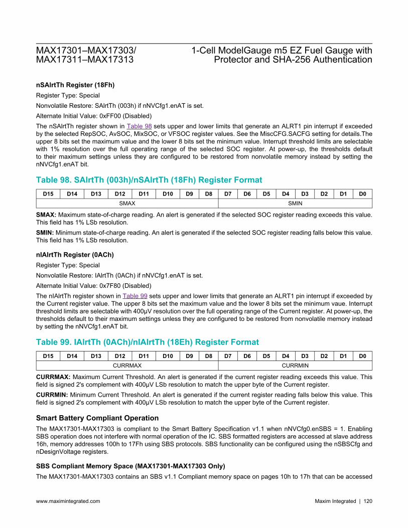
nSAlrtTh Register (18Fh) Register Type: Special Nonvolatile Restore: SAlrtTh (003h) if nNVCfg1.enAT is set. Alternate Initial Value: 0xFF00 (Disabled) The nSAlrtTh register shown in Table 98 sets upper and lower limits that generate an ALRT1 pin interrupt if exceeded by the selected RepSOC, AvSOC, MixSOC, or VFSOC register values. See the MiscCFG.SACFG setting for details.The upper 8 bits set the maximum value and the lower 8 bits set the minimum value. Interrupt threshold limits are selectable with 1% resolution over the full operating range of the selected SOC register. At power-up, the thresholds default to their maximum settings unless they are configured to be restored from nonvolatile memory instead by setting the nNVCfg1.enAT bit.
Table 98. SAlrtTh (003h)/nSAlrtTh (18Fh) Register Format D15 D14 D13 D12 D11 D10 D9 D8 D7 D6 D5 D4 D3 D2 D1 D0
SMAX SMIN
SMAX: Maximum state-of-charge reading. An alert is generated if the selected SOC register reading exceeds this value. This field has 1% LSb resolution. SMIN: Minimum state-of-charge reading. An alert is generated if the selected SOC register reading falls below this value. This field has 1% LSb resolution.
nIAlrtTh Register (0ACh) Register Type: Special Nonvolatile Restore: IAlrtTh (0ACh) if nNVCfg1.enAT is set. Alternate Initial Value: 0x7F80 (Disabled) The nIAlrtTh register shown in Table 99 sets upper and lower limits that generate an ALRT1 pin interrupt if exceeded by the Current register value. The upper 8 bits set the maximum value and the lower 8 bits set the minimum vaue. Interrupt threshold limits are selectable with 400μV resolution over the full operating range of the Current register. At power-up, the thresholds default to their maximum settings unless they are configured to be restored from nonvolatile memory instead by setting the nNVCfg1.enAT bit.
Table 99. IAlrtTh (0ACh)/nIAlrtTh (18Eh) Register Format D15 D14 D13 D12 D11 D10 D9 D8 D7 D6 D5 D4 D3 D2 D1 D0
CURRMAX CURRMIN
CURRMAX: Maximum Current Threshold. An alert is generated if the current register reading exceeds this value. This field is signed 2's complement with 400μV LSb resolution to match the upper byte of the Current register. CURRMIN: Minimum Current Threshold. An alert is generated if the current register reading falls below this value. This field is signed 2's complement with 400μV LSb resolution to match the upper byte of the Current register.
Smart Battery Compliant Operation The MAX17301-MAX17303 is compliant to the Smart Battery Specification v1.1 when nNVCfg0.enSBS = 1. Enabling SBS operation does not interfere with normal operation of the IC. SBS formatted registers are accessed at slave address 16h, memory addresses 100h to 17Fh using SBS protocols. SBS functionality can be configured using the nSBSCfg and nDesignVoltage registers.
SBS Compliant Memory Space (MAX17301-MAX17303 Only) The MAX17301-MAX17303 contains an SBS v1.1 Compliant memory space on pages 10h to 17h that can be accessed
MAX17301–MAX17303/MAX17311–MAX17313
1-Cell ModelGauge m5 EZ Fuel Gauge withProtector and SHA-256 Authentication
www.maximintegrated.com Maxim Integrated | 120

using the Read Word, Write Word, and Read Block commands at 2-Wire slave address 16h. Table 100 lists the SBS compliant registers. Refer to the SBS 1.1 Specification for details of registers at addresses 100h to 12Fh. Registers marked with Note 3 in the table are shared between SBS and normal IC functions and are always readable regardless of IC settings. Their format is described in the Analog Measurements section of the data sheet. All other registers on pages 13h to 17h are described in this section. Greyed locations are reserved and should not be written to.
Table 100. SBS Register Space Memory Map
PAGE/ WORD
10xH 11xH 12xH 13xH 14xH 15xH 16xH 17xH
0h sManfctAccess sFullCap sManfctrName1 — — — — sManfctInfo2
1h sRemCapAlarm sRunTTE sDeviceName1 — — — — — 2h sRemTimeAlarm sAvgTTE sDevChemistry1 — — — — — 3h sBatteryMode sAvgTTF sManfctData2 — — — — — 4h sAtRate sChargingCurrent — Temp13 — — — — 5h — sChargingVoltage — IntTemp3 — — — — 6h sAtTTE sBatteryStatus — sFirstUsed — — — — 7h sAtRateOK sCycles — AvgTemp13 — — sAvCap — 8h sTemperature sDesignCap — AvgIntTemp3 — — sMixCap — 9h sPackVoltage sDesignVolt — — — — — —
Ah sCurrent sSpecInfo — — — — — —
Bh sAvgCurrent sManfctDate — — — — — — Ch sMaxError sSerialNumber2 — — — — — — Dh sRelSOC — — — — — CGTempCo3 — Eh sAbsSOC — — — — — — — Fh sRemCap — — sCell1 sAvgCell1 — — —
1. Location is read as ASCII data using the Read Block command. 2. Location is read as Hexadecimal data using the Read Block command. 3. Location is shared between SBS and normal IC functions and is always readable regardless of IC settings.
sRemCapAlarm/sRemTimeAlarm Registers (101h/102h) Register Type: Capacity/Time Nonvolatile Restore: None sRemCapAlarm: sRemCapAlarm defaults to DesignCap/10 at startup. sRemTimeAlarm: sRemTimeAlarm defaults to 10min at startup.
At-Rate Functionality
sAtRate Register (104h) Register Type: Current Nonvolatile Backup: None Host software should write the sAtRate register with a negative two’s-complement 16-bit value of a theoretical load
MAX17301–MAX17303/MAX17311–MAX17313
1-Cell ModelGauge m5 EZ Fuel Gauge withProtector and SHA-256 Authentication
www.maximintegrated.com Maxim Integrated | 121

current prior to reading any of the at-rate output registers. AtRate calculations are performed using sAtRate (0x104) if enSBS = 1, or AtRate(0x004) if enSBS = 0.
sAtTTF Register (105h) Register Type: Time Nonvolatile Backup: None The sAtTTF register can be used to estimate time to full for any theoretical current load entered into the sAtRate register. AtRate calculations are performed using either sAtRate (0x104) if enSBS = 1, or AtRate(0x004) if enSBS = 0.
sAtTTE Register (105h) Register Type: Time Nonvolatile Backup: None The sAtTTE register can be used to estimate time-to-empty for any theoretical current load entered into the sAtRate register. The AtTTE register displays the estimated time-to-empty for the application by dividing AtAvCap by the sAtRate register value. sAtTTE is translated from AtTTE for conversion into minutes. AtRate calculations are performed using either sAtRate (0x104) if enSBS = 1, or AtRate(0x004) if enSBS = 0.
sAtRateOK Register (107h) Register Type: Special Nonvolatile Restore: None From SBS spec AtRateOK: Description: Returns a Boolean value that indicates whether or not the battery can deliver the previously written AtRate value of additional energy for 10 seconds (Boolean). If the AtRate value is zero or positive, the AtRateOK function ALWAYS returns true. Result may depend on the setting of CAPACITY_MODE bit. Purpose: The AtRateOK function is part of a two-function call-set used by power management systems to determine if the battery can safely supply enough energy for an additional load. It is used immediately after the SMBus host sets the AtRate value. Refer to AtRate for additional usage information.
sTemperature Register (108h) Register Type: Temperature Nonvolatile Restore: None Temperature is translated from AvgTA register.
sPackVoltage Register (109h) Register Type: Voltage Nonvolatile Restore: None Voltage is translated from sCELL1.
sChargingCurrent Register (114h) Register Type: Current Nonvolatile Restore: None As for the SBS, this register returns the smart battery's desired charging rate in mA.
MAX17301–MAX17303/MAX17311–MAX17313
1-Cell ModelGauge m5 EZ Fuel Gauge withProtector and SHA-256 Authentication
www.maximintegrated.com Maxim Integrated | 122

sDesignVolt Register (119h) Register Type: Voltage Nonvolatile Restore: None sDesignVolt is represented per cell.
sSpecInfo Register (11Ah) Register Type: Special Nonvolatile Backup: None
Table 101. SpecInfo (11Ah) Format D15 D14 D13 D12 D11 D10 D9 D8 D7 D6 D5 D4 D3 D2 D1 D0
0 0 0 0 0 0 0 0 0 0 1 1 (PEC) 0 0 0 1
PEC: PEC indicates whether the pack is configured to support SMBus PEC correction. PEC is always enabled on the MAX17301-MAX17303 in SBS Mode.
sSerialNumber Register (11Ch to 11Eh) Register Type: Special Nonvolatile Restore: None SerialNumber indicates the 16-bit serial number as stored in nSerialNumber MTP. SerialNumber2 and 3 provide extended data for the serial number as stored in nSerialNumber2 and nSerialNumber3. By using 6-bytes total, a serial number can provide a very unique ID for 281 trillion devices. A 4-byte serial number can support 4.3 billion devices. Some of the bits can be fixed to indicate platform or other information.
sManfctrName Register (120h) Register Type: Special Nonvolatile Restore: nManfctrName A block SMBus/I2C read of 0x20 on I2C slave 0x16 (SBS) reports RAM addresses 0x120 sequenced with 0x146-0x14A, for a total of 6-words of data. The first byte indicates the byte length and the following bytes are ASCII characters representing the brand name of the pack. This data is taken from nManfctrName MTP, except that the byte count is set by firmware instead of saved in MTP.
sDeviceName Register (121h) Register Type: Special Nonvolatile Restore: nDeviceName A block SMBus/I2C read of 0x21 on I2C slave 0x16 (SBS) reports RAM addresses 0x121 sequenced with 0x140 to 0x143, for a total of 5-words of data. The first byte indicates the byte length and the following bytes are ASCII characters representing the device name. This data is taken from nDeviceName MTP, except that the byte-count is set by firmware instead of saved in MTP.
sDevChemistry Register (122h) Register Type: Special Nonvolatile Restore: None A block SMBus/I2C read of 0x22 on I2C slave 0x16 (SBS) reports RAM addresses 0x122 sequenced with 0x156 to 0x158, for a total of 4-words of data. The first byte indicates the byte length and the following bytes are ASCII characters representing the device chemistry. For the MAX1730x/MAX1731x this string is always “LION”, which is standard for all SBS packs.
MAX17301–MAX17303/MAX17311–MAX17313
1-Cell ModelGauge m5 EZ Fuel Gauge withProtector and SHA-256 Authentication
www.maximintegrated.com Maxim Integrated | 123

sManfctData Registers (123h to 12Fh) Register Type: Various Nonvolatile Restore: None The bytes of this read-block command are defined as follows: Byte 0: Cell count. Copy from NCELLS information. Byte 1: High-Byte of eep_MEM_VER Byte 2: Low-byte of eep_MEM_VER Byte 3: High-Byte of Version Byte 4: Low-Byte of Version Byte 5: HCONFIG Byte 6: HCONFIG2 Byte 7: Q Byte 8: QH
sFirstUsed Register (136h) This register contains a mirror of the value stored in nonvolatile memory address 1D7h.
sCell1 Register (13Fh) This register contains the same cell voltage information displayed in Cell1 (0D8h) respectively with SBS compliant formatting. 1 LSb = 1mV giving a full scale range of 0.0V to 65.535V.
sAvgCell1 Register (14Fh) This register contains the same average cell voltage information displayed in AvgCell1 (0D4h) with SBS compliant formatting. 1 LSb = 1mV giving a full scale range of 0.0V to 65.535V.
sAvCap Register (167h) This register contains the same information as the AvCap (01Fh) register. It is formatted for SBS compliance where 1 LSb = 1.0mAh giving a full scale range of 0.0mAh to 65535mAh.
sMixCap Register (168h) This register contains the same information as the MixCap (00Fh) register. It is formatted for SBS compliance where 1 LSb = 1.0mAh giving a full scale range of 0.0mAh to 65535mAh.
sManfctInfo Register (170h) The sManfctInfo register is accessed using the SBS protocol read block command. This register function is not supported in the MAX1730x/MAX1731x.
Nonvolatile SBS Register Back-Up When SBS mode operation is enabled by setting nNVCfg0.enSBS = 1, data from several nonvolatile memory locations is translated into SBS memory space. Table 102 lists these translations. Note that when performing an SBS Read Block command, the IC automatically generates the size data byte by counting the number of sequential non-zero data bytes stored in the corresponding nonvolatile memory locations. The nonvolatile memory only needs to store the actual data to be read by an SBS Read Block command. If SBS mode of operation is disabled, these locations become available for general purpose nonvolatile data storage.
MAX17301–MAX17303/MAX17311–MAX17313
1-Cell ModelGauge m5 EZ Fuel Gauge withProtector and SHA-256 Authentication
www.maximintegrated.com Maxim Integrated | 124

Table 102. SBS to Nonvolatile Memory Mapping NONVOLATILE MEMORY
ADDRESS NONVOLATILE MEMORY REGISTER
NAME SBS MEMORY
ADDRESS S REGISTER
NAME 1D6h nManfctrDate 1Bh sManfctrDate 1D7h nFirstUsed 36h sFirstUsed
1CCh-1CEh nManfctrName[2:0] 20h
(Read Block Command) sManfctrName
1D8h-1DAh nSerialNumber[2:0] 1Ch
(Read Block Command) sSerialNumber
1DBh-1DFh nDeviceName[4:0] 21h
(Read Block Command) sDeviceName
nSBSCfg Register (1B4h) Register Type: Special Nonvolatile Restore: There is no associated restore location for this register. The nSBSCfg register manages settings for SBS mode operation of the IC. If nNVCfg0.enSBS = 0 and SBS mode is not used, this register can be used as general purpose data storage. Table 103 shows the register format.
Table 103. nSBSCfg Register (1B4h) Format D15 D14 D13 D12 D11 D10 D9 D8 D7 D6 D5 D4 D3 D2 D1 D0
CapMd X X X X X X X X X X X X MECfg X
X: Don’t Care. This bit is undefined and can be logic 0 or 1. MECfg: Configures sMaxError register output when operating in SBS mode. 00: Always report 0% error 01: Always report 1% error 10: Report actual experienced error 11: Always report 3% error CapMd: Selects sBatteryMode.CapMd bit default setting when operating in SBS mode. CapMd resets to 0 every time a pack removal occurs as detected by floating communication lines.
nCGain and Sense Resistor Relationship To meet SBS compliance, current and capacity registers in the SBS memory space must have an LSb bit weight of 1.0mA or 1.0mAh. The current gain must be adjusted based on the application sense resistor value to set the proper bit weight. Table 104 shows the proper nCGain value to use for the most common sense resistor values. This is the default register value only. It does not include any offset trim or custom gain adjustment. Note that changing the nCGain register affects the gain reported by the standard ModelGauge current and capacity registers.
MAX17301–MAX17303/MAX17311–MAX17313
1-Cell ModelGauge m5 EZ Fuel Gauge withProtector and SHA-256 Authentication
www.maximintegrated.com Maxim Integrated | 125

Table 104. nCGain Register Settings to Meet SBS Compliance SENSE RESISTOR VALUE (Ω) NCGAIN REGISTER VALUE CORRESPONDING CGAIN REGISTER VALUE
0.0025 0x4000 0x0400 0.005 0x2000 0x0200 0.010 0x1000 0x0100
Dynamic Battery Power Technology (DBPT) Registers Many mobile systems with high-performance CPUs, GPUs, motors, radios, etc., require the battery to deliver short pulses of high power without the battery voltage falling below critical system undervoltage levels. Managing these pulse loads optimally without sacrificing performance is quite challenging without appropriate battery capability information being available to the system. To achieve better run-time and to help the system run at optimal performance, Maxim has developed Dynamic Battery Power Technology (DBPT). MAX17301–MAX17303/MAX17311–MAX17313 supports this DBPT feature, which provides the on-demand battery capability to be used for managing pulse-loads. To support these high pulses without the battery voltage falling below critical system under-voltage levels, the MAX1730x/MAX1731x indicates the instantaneous peak and sustained power levels that can be extracted safely from the battery. The system can use this information to set its maximum current in accordance with battery power capability. For example, in many 1-cell applications, the system requires at least 3.3V to operate correctly. By configuring the MAX1730x/MAX1731x for DBPT, the system's loads can be controlled or limited to stay within the battery's capability and ensure that a minimum system voltage (MinSysVolt) is not crossed until the battery is a very low state. The implementation of DBPT in the MAX1730x/MAX1731x hews closely to Intel's Dynamic Battery Power Technology v2.0 standard and relies on specific functions and corresponding registers. This section defines those functions. The implementation in the MAX1730x/MAX1731x includes all the same registers as the Intel spec. However, the MAX1730x/MAX1731x register set uses different LSBs and addresses from the Intel standard. The following registers are used for DBPT. The units of the DBPT registers are not SBS compatible. The MAX1730x/MAX1731x uses an LSB of 1mV for voltage, 1mA for current, 10mW for power, and 1mΩ for resistance. Additionally, although SMBus is used as the underlying physical layer for these new functions, the functions are available with the Maxim 1-Wire or 2-Wire (I2C) Interface.
MaxPeakPower Register (0A4h) Specification Description: The fuel gauge computes and return the maximum instantaneous peak output power of the battery pack in cW, which is available for up to 10ms, given the external resistance and required minimum voltage of the voltage regulator. The MaxPeakPower value is expected to be negative and has to be updated at least once every second. MaxPeakPower is initialized to the present value of MaxPeakPower on reset or power-up. Internal configuration of the fuel gauge should allow the maximum value of this parameter to be configured which account for various system limitations, such as limiting the cell discharge current to the 4C rate, and allowing for the safe operating area specifications for devices in the power path, such as MOSFETs. It is suggested that these parameters be user definable. LSB is 10mW. Actual Calculation: MaxPeakPower = MPPCurrent x AvgVCell
SusPeakPower Register (0A5h) Specification Description:
MAX17301–MAX17303/MAX17311–MAX17313
1-Cell ModelGauge m5 EZ Fuel Gauge withProtector and SHA-256 Authentication
www.maximintegrated.com Maxim Integrated | 126

The fuel gauge computes and returns the sustained peak output power of the battery pack in cW, which is available for up to 10s, given the external resistance and required minimum voltage of the voltage regulator. The SusPeakPower value is expected to be negative and has to be updated at least once every second. SusPeakPower is initialized to the present value of SusPeakPower on reset or power-up. Internal configuration of the fuel gauge should allow the maximum value of this parameter to be configured which accounts for various system limitations, such as limiting the cell discharge current to the 2C rate, and allowing for the safe operating area specifications for devices in the power path, such as MOSFETs. It is suggested that these parameters be user definable. LSB is 10mW. Actual Calculation: SusPeakPower = SPPCurrent x AvgVCell
sPackResistance (0A6h) and nPackResistance (1C5h) Specification Description: This function reports the total noncell pack resistance value to account for the resistances due to cell interconnect, sense resistor, FET, fuse, connector, and other impedances between the cells and output of the battery pack. The cell internal resistance should NOT be included. PackResistance is set at time of pack manufacture. Writes to this value has no change to the value during normal operation. This value is usually determined by the battery pack manufacturer and set at time of pack manufacture. The pack-maker can configure PackResistance by programming the nonvolatile nPackResistance during production. LSB of 1mΩ per LSB.
SysResistance (0A7h) Specification Description: This function is to write the total resistance value into fuel gauge to account for the resistances due to the resistance of power/ground metal, sense resistor, FET, and other parasitic resistance on the system main board. SysResistance is initialized to a default value upon removal or insertion of a battery pack. Writes with this function overwrites the default value. The system designer is expected to overwrite the default value with the value from the system in question. This allows a single pack to be used in multiple systems which may have various values for SysResistance. 1mΩ per LSB.
sMPPCurrent (0A9h) Specification Description: The fuel gauge computes and returns the maximum instantaneous peak current of the battery pack in mA, which is available for up to 10ms, given the external resistance and required minimum voltage of the voltage regulator. The MPPCurrent value is expected to be negative and has to be updated at least once every second. MPPCurrent is initialized to the present value of MPPCurrent on reset or power-up. Actual Calculation: MPPCurrent = (AvgVCell - MinSySVoltage)/[(PackResistance + SysResistance) x Rgain1]
SPPCurrent (0AAh) Specification Description: The fuel gauge computes and returns the sustained peak current of the battery pack in mA, which is available for up to 10s, given the external resistance and required minimum voltage of the voltage regulator. The SPPCurrent value is expected to be negative and has to be updated at least once every second. SPPCurrent is initialized to the present value of SPPCurrent on reset or power-up. Actual Calculation:
MAX17301–MAX17303/MAX17311–MAX17313
1-Cell ModelGauge m5 EZ Fuel Gauge withProtector and SHA-256 Authentication
www.maximintegrated.com Maxim Integrated | 127

SPPCurrent = (AvgVCell - MinSySVoltage)/(RCell x Rgain2)
nDPLimit Register (1E0h) Register Type: Special Initial Value: 0x8040 The nDPLimit register sets the safety limits for Dynamic Power Max-Peak Power and Max-Sustained Power. Table 105 shows the register format.
Table 105. nDPLimit (1E0h) Format D15 D14 D13 D12 D11 D10 D9 D8 D7 D6 D5 D4 D3 D2 D1 D0
MPPLimit SPPLimit
Both MPPLimit and SPPLimit are expressed as positive unsigned numbers, although they're used to limit negative discharge currents. MPPLimit: MPPCurrent C-Rate Limit. 0x20 is the setting for 1C current limit. The LSB is C/32 for a range from 0C to 7.97C. SPPLimit: SPPCurrent C-Rate Limit. 0x40 is the setting for 1C current limit. The LSB is C/64 for a range from 0C to 3.98C. Be sure to set MPPLimit and SPPLimit to be under the ADC range for current measurements.
SHA-256 Authentication The MAX17301/MAX17302/MAX17311/MAX17312 supports authentication which is performed using a FIPS 180-4 compliant SHA-256 one-way hash algorithm on a 512-bit message block. The message block consists of a 160-bit secret, a 160-bit challenge, and 192 bits of constant data. Optionally, the 64-bit ROM ID replaces 64 of the 192 bits of constant data used in the hash operation. Contact Maxim for details of the message block organization. The host and the IC both calculate the result based on the mutually known secret. The result of the hash operation is known as the message authentication code (MAC) or message digest. The MAC is returned by the IC for comparison to the host’s MAC. Note that the secret is never transmitted on the bus and thus cannot be captured by observing bus traffic. Each authentication attempt is initiated by the host system by writing a 160-bit random challenge into the SHA memory address space 0C0h to 0C9h. The host then issues the compute MAC or compute MAC with ROM ID command. The MAC is computed per FIPS 180-4 and stored in address space 0C0h to 0CFh overwriting the challenge value. The MAX17301/MAX17302/MAX17311/MAX17312 introduces the new MAC key derivation function (MKDF), a 2-stage authentication scheme that utilizes an intermediate secret for an added layer of security. Note that the results of the authentication attempt are determined by host verification. Operation of the IC is not affected by authentication success or failure.
Authentication Procedure Figure 25 shows how a host system verifies the authenticity of a connected battery. The host first generates a random 160-bit challenge value and writes the challenge to IC memory space 0C0h to 0C9h. The host then sends the Compute MAC with ROM ID (3500h) or Compute MAC without ROM ID (3600h) to the Command register 060h and wait tSHA for computation to complete. Finally, the host reads the MAC from memory space 0C0h to 0CFh to verify the result. This procedure requires the secret to be maintained on the host side as well as in the battery. The host must perform the same calculations in parallel to verify the battery is authentic.
MAX17301–MAX17303/MAX17311–MAX17313
1-Cell ModelGauge m5 EZ Fuel Gauge withProtector and SHA-256 Authentication
www.maximintegrated.com Maxim Integrated | 128

Procedure to Verify a Battery
MACs MATCHACCEPT
BATTERY
MACs DO NOT MATCH
REJECT BATTERY
RANDOM CHALLENGE GENERATION
SECRETSECRET
MAC COMPUTATIONPARALLEL
COMPUTATION
VERIFICATION BATTERY
HOST
Figure 25. Procedure to Verify a Battery
Alternate Authentication Procedure Figure 26 shows an alternative method of battery authentication which does not require the host to know the secret. In this method, each host device knows a challenge and MAC pair that matches the secret stored in an authentic battery, but each host device uses a different pair. This eliminates the need for special hardware on the host side to protect the secret from hardware intrusion. A battery could be cloned for a single host device, but creating a clone battery that works with any host would not be possible without knowing the secret. The authentication process for this method is less complex. The host simply writes the challenge to IC memory space 0C0h to 0C9h. The host then sends the Compute MAC without ROM ID (3600h) to the Command register 060h. Note that Compute MAC with ROM ID Command is not valid for this authentication method. The host then waits tSHA for computation to complete and reads the MAC from memory space 0C0h to 0CFh to verify the result.
MAX17301–MAX17303/MAX17311–MAX17313
1-Cell ModelGauge m5 EZ Fuel Gauge withProtector and SHA-256 Authentication
www.maximintegrated.com Maxim Integrated | 129

Battery Authentication without a Host Side Secret
SECRETMAC 1
VERIFICATION
HOST 1
MAC COMPUTATION
CHALLENGE 1
PASS FAIL
VALID BATTERY
SECRETMAC 2
VERIFICATION
HOST 2
MAC COMPUTATION
CHALLENGE 2
PASS FAIL
VALID BATTERY
SECRETMAC N
VERIFICATION
HOST N
MAC COMPUTATION
CHALLENGE N
PASS FAIL
VALID BATTERY
Figure 26. Battery Authentication without a Host Side Secret
Secret Management The secret value must be programmed to a known value prior to performing authentication in the application. The secret cannot be written directly. Instead, the user must generate a new internal secret by performing a SHA computation with the old internal secret and a seed value sent as a challenge. To prevent any one entity from knowing the complete secret value, the process can be repeated multiple times by sending additional challenge seeds and performing additional computations.
MAX17301–MAX17303/MAX17311–MAX17313
1-Cell ModelGauge m5 EZ Fuel Gauge withProtector and SHA-256 Authentication
www.maximintegrated.com Maxim Integrated | 130

Note that secret memory can only be changed a maximum of nSECRET times including erase operations and nonvolatile memory updates are not guaranteed. See the nSECRET write limit in the Electrical Characteristics table. Any secret update operation that fails does not change the secret value stored in the IC, but consumes one of the available limited updates. Be careful not to use up all secret memory during the generation process. Maxim strongly recommends permanently locking the secret after it has been generated.
Single Step Secret Generation The single step secret generation procedure should be used in production environments where the challenge seed value can be kept confidential, for example, when there are no OEM manufacturing steps or situations where an outside individual or organization would need to know the challenge seed. Use the following sequence to program the IC. Since the secret cannot be read from the IC, a parallel computation must be performed externally in order to calculate the stored secret. Figure 27 shows an example single step secret generation operation. Note that new units have their secret value already cleared to all 0s.
1. Clear the CommStat.NVError bit. 2. Write a challenge seed value to the SHA memory space 0C0h to 0C9h. 3. Write Compute Next Secret with ROM ID 3300h or Compute Next Secret without ROM ID 3000h to the
Command register 060h. 4. Wait tSHA + tUPDATE for computation to complete and new secret to be stored. 5. If CommStat.NVError is set, return to step 1, otherwise, continue. 6. Verify the secret has been generated correctly with a test challenge at this time. If verification fails, return to
step 1. See the Determining Number of Remaining Updates section to verify enough nonvolatile memory writes remain in order to repeat the process.
7. Write Lock Secret 6000h to the Command register 060h. Note this operation cannot be reversed. 8. Wait tUPDATE for secret to lock permanently.
Single Step Secret Generation Example
BATTERY
COMPUTE NEXT
FINAL SECRET
STARTING SECRET CLEARED
TO ALL 0s
FINAL SECRET
SEED
PARALLEL COMPUTATION
Figure 27. Single Step Secret Generation Example
MAX17301–MAX17303/MAX17311–MAX17313
1-Cell ModelGauge m5 EZ Fuel Gauge withProtector and SHA-256 Authentication
www.maximintegrated.com Maxim Integrated | 131

Multistep Secret Generation Procedure The multistep secret generation procedure should be used in environments where an outside individual or organization would need to know the challenge seed such as OEM manufacturing. The multistep procedure is more complicated but allows a secret to be stored inside the IC without providing any information to an OEM manufacturer that could jeopardize secret integrity. Figure 28 shows an example where three OEM manufacturers are each provided with a seed value for a Compute Next operation. The final secret value stored inside the IC are known only to the top level manager who knows all seed values and has performed the computation separately. Use the following procedures when generating a multi-step secret. Note that the secret can only be updated or cleared nSECRET times total. New units have their secret value already cleared to all 0s. All OEMs:
1. Clear the CommStat.NVError bit. 2. Write challenge seed value to the SHA memory space 0C0h to 0C9h. 3. Write Compute Next Secret with ROM ID 3300h or Compute Next Secret without ROM ID 3000h to the
Command register 060h. 4. Wait tSHA + tUPDATE for computation to complete and new secret to be stored. 5. If CommStat.NVError is set, return to step 1, otherwise, continue. 6. Verify the secret has been generated correctly with a test challenge at this time. If verification fails, return to
step 1. See the Determining Number of Remaining Updates section to verify enough nonvolatile memory writes remain in order to repeat the process.
Last OEM:
1. Follow the procedure above for the final secret update. 2. Write Lock Secret 6000h to the Command register 060h. Note this operation cannot be reversed. 3. Wait tUPDATE for secret to lock permanently.
Top Level:
1. Generate all seed values to provide to OEMs. 2. Perform SHA calculations seperately to determine what the final secret is after all manufacturing steps. 3. Keep final secret value secure.
MAX17301–MAX17303/MAX17311–MAX17313
1-Cell ModelGauge m5 EZ Fuel Gauge withProtector and SHA-256 Authentication
www.maximintegrated.com Maxim Integrated | 132

Multistep Secret Generation Example
SEED 1
BATTERY
COMPUTE NEXT
MIDDLE SECRET 1
STARTING SECRET CLEARED TO ALL
0s
CHALLENGE 1 AND MAC 1 FOR
VERIFICATION
OEM 1
SEED 2
BATTERY
COMPUTE NEXT
MIDDLE SECRET 2
MIDDLE SECRET 1
CHALLENGE 2 AND MAC 2 FOR
VERIFICATION
OEM 2
SEED 3
BATTERY
COMPUTE NEXT
FINAL SECRET
MIDDLE SECRET 2
CHALLENGE 3 AND MAC 3 FOR
VERIFICATION
OEM 3
SEED 1 GENERATION
SEED 3 GENERATION
FINAL SECRET
MIDDLE SECRET 1 COMPUTATION
MIDDLE SECRET 2 COMPUTATION
SEED 3 GENERATION
TOP
LEV
EL P
RO
JEC
T M
AN
AG
ER
Figure 28. Multistep Secret Generation Example
2-Stage MKDF Authentication Scheme The MAX17301/MAX17302/MAX17311/MAX17312 introduces the new 2-stage MKDF authentication scheme that utilizes an intermediate secret for an added layer of security. Figure 29 illustrates how to create a unique intermediate secret that can be stored in the host at the factory. Figure 30 outlines the procedure to complete the 2-stage authentication. The following procedure implements the MKDF authentication scheme:
1. Write Copy Intermediate Secret from NVM command 3800h to the Command register 060h. 2. Write unique challenge seed value to the SHA memory space 0C0h to 0C9h to be used to compute the next
intermediate secret. 3. Write Compute Next Intermediate Secret with ROM ID 3900h or Compute Next Intermediate Secret without
ROM ID 3A00h to the Command register 060h.
MAX17301–MAX17303/MAX17311–MAX17313
1-Cell ModelGauge m5 EZ Fuel Gauge withProtector and SHA-256 Authentication
www.maximintegrated.com Maxim Integrated | 133

4. Wait tSHA for computation to complete. 5. Write challenge seed value to the SHA memory space 0C0h to 0C9h to be used to compute MAC using the
intermediate secret. 6. Write Compute MAC From Intermediate Secret with ROM ID 3D00h or Compute MAC From Intermediate
Secret without ROM ID 3C00h to the Command register 060h. 7. Wait tSHA for computation to complete. 8. Read the MAC from SHA memory space 0C0h to 0CFh to verify the result.
Because the intermediate secret is stored in the same RAM location used for SHA calculation, executing some commands overwrites the intermediate secret. The functional impact is summarized as follows: Compute MAC and Compute Next Secret commands overwrites the intermediate secret. Copy intermediate secret from NVM overwrites the intermediate secret (as expected). Compute MAC from intermediate secret also overwrites the intermediate secret. If an intermediate secret is used for
multiple MAC calculations, the intermediate secret needs to be reconstructed after each MAC computation.
Create a Unique Intermediate Secret
UNIQUE INTERMEDIATE SECRET
SECRET
COMPUTE NEXT SECRET
UNIQUE CHALLENGE
FACTORY (ONCE PER HOST)
Figure 29. Create a Unique Intermediate Secret
MAX17301–MAX17303/MAX17311–MAX17313
1-Cell ModelGauge m5 EZ Fuel Gauge withProtector and SHA-256 Authentication
www.maximintegrated.com Maxim Integrated | 134

Procedure for 2-Stage MKDF Authentication
MACs MATCHACCEPT
BATTERY
MACs DO NOT MATCH
REJECT BATTERY
RANDOM CHALLENGE GENERATION
UNIQUE INTERMEDIATE SECRET
MAC COMPUTATION FROM INTERMEDIATE SECRET
PARALLEL COMPUTATION
VERIFICATION BATTERY
HOST
SECRETUNIQUE CHALLENGE STEP 1
STEP 2
STEP 3
UNIQUE INTERMEDIATE SECRET
COMPUTE NEXT INTERMEDIATE
SECRET
Figure 30. Procedure for 2-Stage MKDF Authentication
Determining Number of Remaining Updates The internal secret can only be updated or cleared nSECRET times total. The number of remaining updates can be calculated using the following procedure: 1. Write 0xE29D to the Command register (060h). 2. Wait tRECALL. 3. Read memory address 1FDh. 4. Decode address 1FDh data as shown in Table 106. Each secret update has redundant indicator flags for reliability.
MAX17301–MAX17303/MAX17311–MAX17313
1-Cell ModelGauge m5 EZ Fuel Gauge withProtector and SHA-256 Authentication
www.maximintegrated.com Maxim Integrated | 135

Logically OR the upper and lower bytes together then count the number of 1s to determine how many updates have already been used. The first update occurs in manufacturing test to clear the secret memory prior to shipping to the user.
Table 106. Number of Remaining Secret Updates ADDRESS 0E6H
DATA LOGICAL OR OF UPPER AND LOWER
BYTES NUMBER OF UPDATES
USED NUMBER OF UPDATES
REMAINING
0000000x00000001b or 000000010000000xb
00000001b 1 5
000000xx0000001xb or 0000001x000000xxb
00000011b 2 4
00000xxx000001xxb or 000001xx00000xxxb
00000111b 3 3
0000xxxx00001xxxb or 00001xxx0000xxxxb
00001111b 4 2
000xxxxx0001xxxxb or 0001xxxx000xxxxxb
00011111b 5 1
00xxxxxx001xxxxxb or 001xxxxx00xxxxxxb
00111111b 6 0
Authentication Commands All SHA authentication commands are written to memory address 060h to perform the desired operation. Writing the Challenge or reading the MAC is handled by accessing the SHA memory space on page 0Ch through direct write and read operations.
COMPUTE MAC WITHOUT ROM ID [3600h] The challenge value must be written to the SHA memory space prior to performing a Compute MAC. This command initiates a SHA-256 computation without including the ROM ID in the message block. Instead, the ROM ID portion of the message block is replaced with a value of all 1s. Since the ROM ID is not used, this command allows the use of a master secret and MAC response independent of the ROM ID. The IC computes the MAC in tSHA after receiving the last bit of this command. After the MAC computation is complete, the host can read the MAC from the SHA memory space.
COMPUTE MAC WITH ROM ID [3500h] The challenge value must be written to the SHA memory space prior to performing a Compute MAC. This command is structured the same as the compute MAC without ROM ID, except that the ROM ID is included in the message block. With the unique ROM ID included in the MAC computation, the MAC is unique to each unit. After the MAC computation
MAX17301–MAX17303/MAX17311–MAX17313
1-Cell ModelGauge m5 EZ Fuel Gauge withProtector and SHA-256 Authentication
www.maximintegrated.com Maxim Integrated | 136

is complete, the host can read the MAC from the SHA memory space.
COMPUTE NEXT SECRET WITHOUT ROM ID [3000h] This command initiates a SHA-256 computation and uses the resulting MAC as the next or new secret. The hash operation is performed with the current 160-bit secret and the new 160-bit challenge. Logical 1s are loaded in place of the ROM ID. The last 160 bits of the MAC are used as the new secret value. The host must allow tSHA after issuing this command for the SHA calculation to complete, then wait tUPDATE for the new secret value to be stored in nonvolatile memory. During this operation, the SHA memory space is not updated. Note that the old secret value must be known prior to executing this command in order to calculate what the new secret value is.
COMPUTE NEXT SECRET WITH ROM ID [3300h] This command initiates a SHA-256 computation and uses the resulting MAC as the next or new secret. The hash operation is performed with the current 160-bit secret, the 64-bit ROM ID, and the new 160-bit challenge. The last 160 bits of the output MAC are used as the new secret value. The host must allow tSHA after issuing this command for the SHA calculation to complete, then wait tUPDATE for the new secret value to be stored in nonvolatile memory. During this operation, the SHA memory space is not updated. Note that the old secret value must be known prior to executing this command in order to calculate what the new secret value is.
CLEAR SECRET [5A00h] This command sets the 160-bit secret to all 0s. The host must wait tUPDATE for the IC to write the new secret value to nonvolatile memory. This command uses up one of the secret write cycles.
LOCK SECRET [6000h] This command write protects the secret to prevent accidental or malicious overwrite of the secret value. The secret value stored in nonvolatile memory becomes permanent. The host must wait tUPDATE for the lock operation to complete. SHA-256 Lock state is not shown in the Lock register. Lock state can be verified by reading nonvolatile memory history using the following sequence: 1. Send 0xE29B to the Command register (060h). 2. Wait for tRECALL. 3. Read memory address 1FCh. If address 1FCh is 0x0000, then the secret is not locked. If address 1FCh is anything other than 0x0000, then the secret is permanently locked.
COPY INTERMEDIATE SECRET FROM NVM [3800] This command copies the secret from NVM and places it in RAM to allow the secret to be used by the other commands.
COMPUTE NEXT INTERMEDIATE SECRET WITH ROMID [3900] This command is similar to COMPUTE NEXT SECRET WITH ROMID except the secret used in the computation comes from the previously executed COPY INTERMEDIATE SECRET FROM NVM or COMPUTE NEXT INTERMEDIATE SECRET WITH/WITHOUT ROMID and the next secret is placed in RAM so it can be used in subsequent commands.
COMPUTE NEXT INTERMEDIATE SECRET WITHOUT ROMID [3A00] This command is similar to COMPUTE NEXT SECRET WITHOUT ROMID except the secret used in the computation comes from the previously executed COPY INTERMEDIATE SECRET FROM NVM or COMPUTE NEXT INTERMEDIATE SECRET WITH/WITHOUT ROMID and the next secret is placed in RAM so it can be used in subsequent commands.
COMPUTE MAC FROM INTERMEDIATE SECRET WITHOUT ROMID [3C00] This command is the same as COMPUTE MAC WITHOUT ROMID except the secret used in the computation comes
MAX17301–MAX17303/MAX17311–MAX17313
1-Cell ModelGauge m5 EZ Fuel Gauge withProtector and SHA-256 Authentication
www.maximintegrated.com Maxim Integrated | 137
from the previously executed COPY INTERMEDIATE SECRET FROM NVM or COMPUTE NEXT INTERMEDIATE SECRET WITH/WITHOUT ROMID.
COMPUTE MAC FROM INTERMEDIATE SECRET WITH ROMID [3D00] This command is the same as COMPUTE MAC WITH ROMID except the secret used in the computation comes from the previously executed COPY INTERMEDIATE SECRET FROM NVM or COMPUTE NEXT INTERMEDIATE SECRET WITH/WITHOUT ROMID.
Device Reset There are two different levels of reset for the IC. A full reset restores the IC to its power-up state the same as if power had been cycled. A fuel-gauge reset resets only the fuel gauge operation without resetting IC hardware. This is useful for testing different configurations without writing nonvolatile memory. Use the following sequences to reset the IC. FULL RESET 1. Reset IC hardware by writing 000Fh to the Command register at 060h. 2. Wait 10mS. 3. Reset IC fuel gauge operation by writing 8000h to the Config2 register at 0ABh. This command does not disturb the state of the protection FETs. 4. Wait for POR_CMD bit (bit 15) of the Config2 register to be cleared to indicate POR sequence is complete. FUEL-GAUGE RESET 1. Reset IC fuel gauge operation by writing 8000h to the Config2 register at 0ABh. This command does not disturb the state of the protection FETs. 2. Wait for POR_CMD bit (bit 15) of the Config2 register to be cleared to indicate POR sequence is complete.
Reset Commands There are two commands that can be used to reset either the entire IC or just the operation of the fuel gauge. Note that the reset fuel gauge command is written to Config2 instead of the Command register.
HARDWARE RESET [000Fh to address 060h] Send the hardware reset command to the Command register to recall all nonvolatile memory into shadow RAM and reset all hardware based operations of the IC. This command should always be followed by the reset fuel gauge command to fully reset operation of the IC.
FUEL GAUGE RESET [8000h to address 0ABh] The fuel-gauge reset command resets operation of the IC without restoring nonvolatile memory values into shadow RAM. This command allows different configurations to be tested without using one of the limited number of nonvolatile memory writes. This command does not disturb the state of the protection FETs.
Communication This section covers communication protocols and summarizes all special commands used by the IC. The MAX17301-MAX17303 communicates over a 2-Wire interface using either I2C or SBS protocols depending on memory address selected by the host. The MAX17311-MAX17313 communicates using the Maxim 1-Wire interface.
2-Wire Bus System The MAX17301-MAX17303 uses a 2-Wire bus system to communicate by both standard I2C protocol or by SBS smart battery protocol. The slave address used by the host to access the IC determines which protocol is used and what memory locations are available to read or write. The following description applies to both protocols. See the I2C and SBS Bus System descriptions for specifc protocol details.
MAX17301–MAX17303/MAX17311–MAX17313
1-Cell ModelGauge m5 EZ Fuel Gauge withProtector and SHA-256 Authentication
www.maximintegrated.com Maxim Integrated | 138

Hardware Configuration The 2-Wire bus system supports operation as a slave-only device in a single or multi-slave, and single or multi-master system. Up to 128 slave devices may share the bus using 7-bit slave addresses. The 2-Wire interface consists of a serial data line (SDA) and serial clock line (SCL). SDA and SCL provide bidirectional communication between the IC and a master device at speeds up to 400kHz. The ICs SDA pin operates bidirectionally. When the IC receives data, SDA operates as an input. When the IC returns data, SDA operates as an open-drain output with the host system providing a resistive pullup. See Figure 31. The IC always operates as a slave device, receiving and transmitting data under the control of a master device. The master initiates all transactions on the bus and generates the SCL signal, as well as the START and STOP bits which begin and end each transaction.
2-Wire Bus Interface Circuitry
VPULLUP
Rx DATA
Tx DATA
Rx DATA
Tx DATARx = RECEIVETx = TRANSMIT
WEAK PULLDOWN
BUS MASTER DEVICE 2-WIRE PORTRPULLUP
DQ/SDA
OD/SCL
Tx CLOCK Rx CLOCK
WEAK PULLDOWN
Figure 31. 2-Wire Bus Interface Circuitry
I/O Signaling The following individual signals are used to build byte level 2-Wire communication sequences.
Bit Transfer One data bit is transferred during each SCL clock cycle, with the cycle defined by SCL transitioning low to high and then high to low. The SDA logic level must remain stable during the high period of the SCL clock pulse. Any change in SDA when SCL is high is interpreted as a START or STOP control signal.
Bus Idle The bus is defined to be idle, or not busy, when no master device has control. Both SDA and SCL remain high when the bus is idle. The STOP condition is the proper method to return the bus to the idle state.
START and STOP Conditions The master initiates transactions with a START condition by forcing a high-to-low transition on SDA while SCL is high. The master terminates a transaction with a STOP condition by a low-to-high transition on SDA while SCL is high. A Repeated START condition can be used in place of a STOP then START sequence to terminate one transaction and begin another without returning the bus to the idle state. In multi-master systems, a Repeated START allows the master to retain control of the bus. The START and STOP conditions are the only bus activities in which the SDA transitions
MAX17301–MAX17303/MAX17311–MAX17313
1-Cell ModelGauge m5 EZ Fuel Gauge withProtector and SHA-256 Authentication
www.maximintegrated.com Maxim Integrated | 139

when SCL is high.
Acknowledge Bits Each byte of a data transfer is acknowledged with an Acknowledge bit (ACK) or a No Acknowledge bit (NACK). Both the master and the IC slave generate acknowledge bits. To generate an Acknowledge, the receiving device must pull SDA low before the rising edge of the acknowledge-related clock pulse (ninth pulse) and keep it low until SCL returns low. To generate a No Acknowledge, the receiver releases SDA before the rising edge of the acknowledge-related clock pulse and leaves SDA high until SCL returns low. Monitoring the acknowledge bits allows for detection of unsuccessful data transfers. An unsuccessful data transfer can occur if a receiving device is busy or if a system fault has occurred. In the event of an unsuccessful data transfer, the bus master should reattempt communication. If a transaction is aborted mid-byte, the master should send additional clock pulses to force the slave IC to free the bus prior to restarting communication.
Data Order With 2-Wire communication, a byte of data consists of 8 bits ordered most significant bit (MSb) first. The least significant bit (LSb) of each byte is followed by the Acknowledge bit. IC registers composed of multibyte values are ordered least significant byte (LSB) first.
Slave Address A bus master initiates communication with a slave device by issuing a START condition followed by a Slave Address and the read/write (R/W) bit. When the bus is idle, the IC continuously monitors for a START condition followed by its slave address. When the IC receives a slave address that matches its Slave Address, it responds with an Acknowledge bit during the clock period following the R/W bit. The MAX17301-MAX17303 supports the slave addresses shown in Table 107.
Table 107. 2-Wire Slave Addresses SLAVE ADDRESS PROTOCOL ADDRESS BYTE RANGE INTERNAL MEMORY RANGE ACCESSED
6Ch I2C 00h-FFh 000h-0FFh
16h SMBUS 00h-7Fh 100h-17Fh
I2C 80h-FFh 180h-1FFh
Read/Write Bit The R/W bit following the slave address determines the data direction of subsequent bytes in the transfer. R/W = 0 selects a write transaction, with the following bytes being written by the master to the slave. R/W = 1 selects a read transaction, with the following bytes being read from the slave by the master.
Bus Timing The IC is compatible with any bus timing up to 400kHz. See the Electrical Characteristics table for timing details. No special configuration is required to operate at any speed. Figure 32 shows an example of standard 2-Wire bus timing.
MAX17301–MAX17303/MAX17311–MAX17313
1-Cell ModelGauge m5 EZ Fuel Gauge withProtector and SHA-256 Authentication
www.maximintegrated.com Maxim Integrated | 140

2-Wire Bus Timing Diagram
SDA
SCL
tF
tRtSU;DAT
tLOW
S
tHD;STAtHD;DAT
tF
tSU;STA
tHD;STA
tSU;STO
tR tBUFtSP
SR P S
Figure 32. 2-Wire Bus Timing Diagram
I2C Protocols The following 2-Wire communication protocols must be used by the bus master to access MAX17301-MAX17303 memory locations 000h to 1FFh. Addresses 000h to 0FFh and from 180h to 1FFh can be read continuously. Addresses 100h to 17Fh must be read one word at a time. These protocols follow the standard I2C specification for communication.
I2C Write Data Protocol The Write Data protocol is used to transmit data to the IC at memory addresses from 000h to 1FFh. Addresses 000h to 0FFh and 180h and 1FFh can be written as a block. Addesses 100h to 17Fh must be written one word at a time. The memory address is sent by the bus master as a single byte value immediately after the slave address. The MSB of the data to be stored is written immediately after the memory address byte is acknowledged. Because the address is automatically incremented after the least significant bit (LSb) of each word received by the IC, the MSB of the data at the next memory address can be written immediately after the acknowledgment of the LSB of data at the previous address. The master indicates the end of a write transaction by sending a STOP or Repeated START after receiving the last acknowledge bit. If the bus master continues an auto-incremented write transaction beyond address 0FFh or 1FFh, the IC ignores the data. Data is also ignored on writes to read-only addresses but not reserved addresses. Do not write to reserved address locations. See Figure 33 for an example Write Data communication sequence.
MAX17301–MAX17303/MAX17311–MAX17313
1-Cell ModelGauge m5 EZ Fuel Gauge withProtector and SHA-256 Authentication
www.maximintegrated.com Maxim Integrated | 141

WRITE DATA COMMUNICATION PROTOCOL
STAR
T SLAVE ADDRESS W
/R =
0
ACK MEMORY
ADDRESS ACK DATA0
LSB ACK DATA0
MSB ACK DATA1
LSB ACK DATA N
MSB ACK
STO
P
EXAMPLE WORD WRITE TO I2C COMMAND REGISTER ADDRESS 060h
STAR
T 6Ch(SLAVE ADDRESS) AC
K
ACK COMMAND
LSB ACK COMMAND
MSB ACK
STO
P60h(MEMORY ADDRESS)
= SLAVE TRANSMISSION = HOST TRANSMISSION
Figure 33. Example I2C Write Data Communication Sequence
I2C Read Data Protocol The Read Data protocol is used to transmit data from IC memory locations 000h to 1FFh. Addresses 000h to 0FFh and 180h to 1FFh can be read as a block. Addresses 100h to 17Fh must be read as individual words. The memory address is sent by the bus master as a single byte value immediately after the slave address. Immediately following the memory address, the bus master issues a REPEATED START followed by the slave address. The MAX17301-MAX17303 ACKs the address and begin transmitting data. A word of data is read as two separate bytes that the master must ACK. Because the address is automatically incremented after the least significant bit (LSb) of each word received by the IC, the MSB of the data at the next memory address can be read immediately after the acknowledgment of the LSB of data at the previous address. The master indicates the end of a read transaction by sending a NACK followed by a STOP. If the bus master continues an auto-incremented read transaction beyond memory address 0FFh or 1FFh, the IC transmits all 1s until a NACK or STOP is received. Data from reserved address locations is undefined. See Figure 34 for an example Read Data communication sequence.
I2C READ DATA COMMUNICATION PROTOCOL
STAR
T SLAVE ADDRESS W
/R =
0
ACK MEMORY
ADDRESS ACK DATA0LSB ACK DATA0
MSB ACK DATA1
LSB ACK DATA N
MSB NAC
K
STO
P
EXAMPLE READ DATA OF CURRENT AND AVGCURRENT REGISTERS ADDRESS 01Ch-01Dh
= SLAVE TRANSMISSION = HOST TRANSMISSION
STAR
T(R
EPEA
TED
) SLAVE ADDRESS W
/R =
1
ACK
1Ch(MEMORY ADDRESS)ST
ART
ACK
ACK Current
LSB ACK Current
MSB ACK
STO
P
STAR
T(R
EPEA
TED
)
ACK6Ch
(SLAVE WRITE ADDRESS)
6Dh(SLAVE READ
ADDRESS)
AvgCurrentLSB AC
K AvgCurrentMSB N
ACK
EXAMPLE READ DATA OF INTTEMP REGISTER ADDRESS 135h
35h(MEMORY ADDRESS)ST
ART
ACK
ACK IntTemp
LSB ACK IntTemp
MSB STO
P
STAR
T(R
EPEA
TED
)
ACK16h
(SLAVE WRITE ADDRESS)
17h(SLAVE READ
ADDRESS) NAC
K
Figure 34. Example I2C Read Data Communication Sequence
SBS Protocols The following 2-Wire communication protocols must be used by the bus master to access MAX17301-MAX17303 memory locations 100h to 17Fh. These protocols follow the smart battery specification for communication.
MAX17301–MAX17303/MAX17311–MAX17313
1-Cell ModelGauge m5 EZ Fuel Gauge withProtector and SHA-256 Authentication
www.maximintegrated.com Maxim Integrated | 142

SBS Write Word Protocol The Write Word protocol is used to transmit data to IC memory addresses between 100h and 17Fh that do not require the Write Block protocol. The memory address is sent by the bus master as a single byte LSB value immediately after the slave address, the MSb of the address is omitted. The LSB of the data to be stored is written immediately after the memory address byte is acknowledged, followed by the MSB. A PEC byte may follow the data word, but the data word is written without checking the validity of the PEC. The master indicates the end of a write transaction by sending a STOP or Repeated START after receiving the last acknowledge bit. Data is ignored on writes to read-only addresses but not reserved addresses. Do not write to reserved address locations. The Write Word protocol should not be used to write to addresses supported by the Write Block protocol, use Write Block at these locations instead. See Figure 35 for an example Write Word communication sequence.
Example SBS Write Word Communication Sequence
SBS WRITE WORD COMMUNICATION PROTOCOL
STAR
T SLAVE ADDRESS W
/R =
1
ACK MEMORY
ADDRESS ACK DATA
LSB ACK DATA
MSB ACK PEC
(OPTIONAL) ACK
STO
P
= SLAVE TRANSMISSION = HOST TRANSMISSION
EXAMPLE WORD WRITE TO SBS ATRATE REGISTER AT REGISTER ADDRESS 104h
STAR
T 16h(SLAVE ADDRESS) AC
K
ACK DATA
LSB ACK DATA
MSB04h
(MEMORY ADDRESS) ACK
STO
P
ACKPEC
(OPTIONAL)
Figure 35. Example SBS Write Word Communication Sequence
SBS Read Word Protocol The Read Word protocol is used to read data from the IC at memory addresses between 100h and 17Fh. The memory address is sent by the bus master as a single byte LSB value immediately after the slave address, the MSb of the address is ignored. The LSB of the data is read immediately after the memory address byte is acknowledged, followed by the MSB. A PEC byte follows the data word. The master indicates the end of a write transaction by sending a STOP or Repeated START after not acknowledging the last received byte. Data from reserved address locations is undefined. The Read Word protocol should not be used to read from addresses supported by the Read Block protocol, use Read Block at these locations instead. See Figure 36 for an example Read Word communication sequence.
MAX17301–MAX17303/MAX17311–MAX17313
1-Cell ModelGauge m5 EZ Fuel Gauge withProtector and SHA-256 Authentication
www.maximintegrated.com Maxim Integrated | 143

Example SBS Read Word Communication Sequence
SBS READ WORD COMMUNICATION PROTOCOL
STAR
T SLAVE ADDRESS W
/R =
1
ACK MEMORY
ADDRESS ACK DATA
LSB ACK DATA
MSB NAC
K
STO
P
= SLAVE TRANSMISSION = HOST TRANSMISSION
STAR
T(R
EPEA
TED
) SLAVE ADDRESS W
/R =
0
ACK
ACK PEC
(OPTIONAL)
EXAMPLE READ WORD OF SBS sTEMPERATURE REGISTER ADDRESS 108h
08h(MEMORY ADDRESS)ST
ART
ACK
ACK sTEMPERATURE
LSB ACK sTEMPERATURE
LSBSTAR
T(R
EPEA
TED
)
ACK16h
(SLAVE WRITE ADDRESS)
17h(SLAVE READ
ADDRESS) NAC
K
STO
P
ACK PEC
(OPTIONAL)
Figure 36. Example SBS Read Word Communication Sequence
SBS Write Block Protocol The SBS Write Block protocol is not supported by the MAX17301-MAX17303. Use the Write Data command sequence to the corresponding nonvolatile memory locations to update Write/Read Block register locations. See Table 100.
SBS Read Block Protocol The Read Block protocol is similar to the Read Word protocol except the master reads multiple words of data at once. A data size byte is transmitted by the IC immediately after the memory address byte and before the first byte of data to be read. The Read Block protocol is only supported at the register locations shown in Table 108. PEC error checking is provided by the Read Block protocol if nNVCfg0.enSBS = 1. Figure 37 shows an example Read Block communication sequence.
Example SBS Read Block Communication Sequence
SBS READ BLOCK COMMUNICATION PROTOCOL
STAR
T SLAVE ADDRESS W
/R =
1
ACK MEMORY
ADDRESS ACK DATA0 ACK DATA (size-2)
NAC
K
STO
PExample Block Read of SBS DevChemistry Register Address 122h
22h(MEMORY ADDRESS)
= SLAVE TRANSMISSION = HOST TRANSMISSION
STAR
T(R
EPEA
TED
) SLAVE ADDRESS W
/R =
0
ACK
STAR
T
ACK
ACK
ACK DATA0
STAR
T(R
EPEA
TED
)
ACK16h
(SLAVE WRITE ADDRESS)
17h(SLAVE READ
ADDRESS)
ACK PEC
(Optional)SIZE AC
K
05h(Size) AC
K DATA3
NAC
K
STO
P
ACK PEC
(Optional)
Figure 37. Example SBS Read Block Communication Sequence
Valid SBS Read Block Registers
Table 108. Valid SBS Read Block Registers ADDRESS REGISTER SIZE BYTE MAX VALUE FORMAT
0120h sManfctName 0Ah ASCII String 0121h sDeviceName 0Ch ASCII String
MAX17301–MAX17303/MAX17311–MAX17313
1-Cell ModelGauge m5 EZ Fuel Gauge withProtector and SHA-256 Authentication
www.maximintegrated.com Maxim Integrated | 144

Table 108. Valid SBS Read Block Registers (continued) ADDRESS REGISTER SIZE BYTE MAX VALUE FORMAT
0122h sDevChemistry 05h ASCII String 0123h sManfctData 1Ah Hexadecimal 011Ch sSerialNumber 08h Hexadecimal 0170h sManfctInfo 18h Hexadecimal
Packet Error Checking SBS read functions support packet error checking (PEC) if nNVCfg0.enSBS is enabled. The host system is responsible for verifying the CRC value it receives and taking action as a result. SBS write functions accept a PEC byte but complete the write function regardless of the value of the PEC. The CRC can be generated by the host using a circuit consisting of a shift register and XOR gates as shown in Figure 38, or it can be generated in software using the polynomial X8 + X2 + X1 + 1. Refer to the Smart Battery Data Specification for more information.
PEC CRC Generation Block Diagram
MSb XOR XOR LSb XOR
INPUT
Figure 38. PEC CRC Generation Block Diagram
1-Wire Bus System (MAX17311-MAX17313 Only) The MAX17311-MAX17313 communicates to a host through a Maxim 1-Wire interface. The 1-Wire bus is a system that has a single bus master and one or more slaves. A multi-drop bus is a 1-Wire bus with multiple slaves, while a single-drop bus has only one slave device. In all instances, this IC is a slave device. The bus master is typically a microprocessor in the host system. The discussion of this bus system consists of five topics: 64-bit net address, CRC generation, hardware configuration, transaction sequence, and 1-Wire signaling.
Hardware Configuration Because the 1-Wire bus has only a single line, it is important that each device on the bus be able to drive it at the appropriate time. To facilitate this, each device attached to the 1-Wire bus must connect to the bus with open-drain or tri-state output drivers. The MAX17311-MAX17313 uses an open-drain output driver as part of the bidirectional interface circuitry shown in Figure 39. If a bidirectional pin is not available on the bus master, separate output and input pins can be connected together. Communication speed is controlled by the OD/SCL pin. Connect OD/SCL to PACK- to enable communication at standard speed. Connect OD/SCL to the REG3 pin to enable communication at overdrive speed. The 1-Wire bus must have a pullup resistor on the host side of the bus. A value between 2kΩ and 5kΩ is recommended for most applications. The idle state for the 1-Wire bus is logic high. If, for any reason, a bus transaction must be suspended, the bus must be left in the idle state to properly resume the transaction later. Note that if the bus is left low for more than tLOW0, slave devices on the bus begin to interpret the low period as a reset pulse, effectively terminating the transaction.
MAX17301–MAX17303/MAX17311–MAX17313
1-Cell ModelGauge m5 EZ Fuel Gauge withProtector and SHA-256 Authentication
www.maximintegrated.com Maxim Integrated | 145

1-Wire Bus Interface Circuitry
VPULLUP
Rx
Tx
Rx
TxRx = RECEIVETx = TRANSMIT
WEAK PULLDOWN
BUS MASTER DEVICE 1-WIRE PORTRPULLUP
DQ/SDA
OVERDRIVE TIMING
0.47µF
OD/SCL
VPULLUP
Rx
Tx
Rx
TxWEAK
PULLDOWN
BUS MASTER DEVICE 1-WIRE PORTRPULLUP
DQ/SDA
STANDARD TIMING
OD/SCL
REG3
Rx = RECEIVETx = TRANSMIT
Figure 39. 1-Wire Bus Interface Circuitry
64-Bit Net Address (ROM ID) The 1-Wire net address is 64 bits in length. The term net address is synonymous with the ROM ID or ROM code terms used in other 1-Wire documentation. The value of the net address is stored in nonvolatile memory and cannot be changed. In a 1-Wire standard net address, the first eight bits of the net address are the 1-Wire family code. This value is the same for all ICs of the same type. The next 48 bits are a unique serial number. The last eight bits are a cyclic redundancy check (CRC) of the first 56 bits. Table 109 details the Net Address data format. The 64-bit net address and the 1-Wire I/O circuitry built into the device enable the MAX1731x to communicate through the 1-Wire protocol detailed in this data sheet.
Table 109. 1-Wire Net Address Format
MSb: 8-Bit CRC 48-Bit Serial Number LSb: 8-Bit Family Code (26h)
I/O Signaling The 1-Wire bus requires strict signaling protocols to ensure data integrity. The four protocols used by the MAX17311-MAX17313 are as follows: the initialization sequence (reset pulse followed by presence pulse), write 0, write 1, and read data. The bus master initiates all signaling except for the presence pulse.
Reset Time Slot The initialization sequence required to begin any communication with the MAX17311-MAX17313 is shown in Figure 40. The bus master transmits (Tx) a reset pulse for tRSTL. The bus master then releases the line and goes into Receive
MAX17301–MAX17303/MAX17311–MAX17313
1-Cell ModelGauge m5 EZ Fuel Gauge withProtector and SHA-256 Authentication
www.maximintegrated.com Maxim Integrated | 146

mode (Rx). The 1-Wire bus line is then pulled high by the pullup resistor. After detecting the rising edge on the DQ pin, the MAX17311-MAX17313 waits for tPDH and then transmits the presence pulse for tPDL. A presence pulse following a reset pulse indicates that the MAX17311-MAX17313 is ready to accept a net address command.
1-Wire Initialization Sequence
tRSTL tRSTH
tPDHVPULLUP
GND
LINE TYPE LEGEND:
BUS MASTER ACTIVE LOW SLAVE IC ACTIVE LOW
BOTH BUS MASTER AND SLAVE IC RESISTOR PULLUPACTIVE LOW
tPDL
Figure 40. 1-Wire Initialization Sequence
Write Time Slots A write-time slot is initiated when the bus master pulls the 1-Wire bus from a logic-high (inactive) level to a logic-low level. There are two types of write-time slots: write 1 and write 0. All write-time slots must be tSLOT in duration with a 1μs minimum recovery time, tREC, between cycles. The MAX17311-MAX17313 samples the 1-Wire bus line between tLOW1_MAX and tLOW0_MIN after the line falls. If the line is high when sampled, a write 1 occurs. If the line is low when sampled, a write 0 occurs. The sample window is illustrated in Figure 41. For the bus master to generate a write-1 time slot, the bus line must be pulled low and then released, allowing the line to be pulled high less than tRDV after the start of the write time slot. For the host to generate a write 0 time slot, the bus line must be pulled low and held low for the duration of the write-time slot.
Read Time Slots A read-time slot is initiated when the bus master pulls the 1-Wire bus line from a logic-high level to a logic-low level. The bus master must keep the bus line low for at least 1μs and then release it to allow the MAX17311-MAX17313 to present valid data. The bus master can then sample the data tRDV from the start of the read-time slot. By the end of the read-time slot, the MAX17311-MAX17313 releases the bus line and allows it to be pulled high by the external pullup resistor. All read-time slots must be tSLOT in duration with a 1μs minimum recovery time, tREC, between cycles. See Figure 41 and the timing specifications in the Electrical Characteristics table for more information.
MAX17301–MAX17303/MAX17311–MAX17313
1-Cell ModelGauge m5 EZ Fuel Gauge withProtector and SHA-256 Authentication
www.maximintegrated.com Maxim Integrated | 147

1-Wire Write and Read Time Slots
LINE TYPE LEGEND:
BUS MASTER ACTIVE LOW SLAVE IC ACTIVE LOW
BOTH BUS MASTER AND SLAVE IC RESISTOR PULLUPACTIVE LOW
MASTER SAMPLE WINDOW
WRITE 0 SLOT WRITE 1 SLOT
tSLOT
tLOW0
tSLOT
tREC
tLOW1
VPULLUP
GND
DEVICE SAMPLE WINDOWMIN TYP MAX
15s
2s
15s 30s
1s 3s
DEVICE SAMPLE WINDOWMIN TYP MAX
15s
2s
15s 30s
1s 3sOVERDRIVE
STANDARD
MODE
>1s
READ DATA SLOT
DATA = 0
tSLOT
15s
tSLOT tREC
VPULLUP
GND
tRDV
15s
MASTER SAMPLE WINDOW
>1s
DATA = 1
OVERDRIVE
STANDARD
MODE
2s 2s
tRDV
Figure 41. 1-Wire Write and Read Time Slots
Transaction Sequence The protocol for accessing the MAX17311-MAX17313 through the 1-Wire port is as follows: Initialization Net Address Command Function Command(s) Data Transfer (not all commands have data transfer)
MAX17301–MAX17303/MAX17311–MAX17313
1-Cell ModelGauge m5 EZ Fuel Gauge withProtector and SHA-256 Authentication
www.maximintegrated.com Maxim Integrated | 148

Net Address Commands Once the bus master has detected the presence of one or more slaves, it can issue one of the net address commands described in the following paragraphs. The name of each net address command (ROM command) is followed by the 8-bit op code for that command in square brackets.
Read Net Address [33h] This command allows the bus master to read the MAX17311-MAX17313’s 1-Wire net address. This command can only be used if there is a single slave on the bus. If more than one slave is present, a data collision occurs when all slaves try to transmit at the same time (open-drain produces a wired-AND result).
Match Net Address [55h] This command allows the bus master to specifically address one MAX17311-MAX17313 on the 1-Wire bus. Only the addressed MAX17311-MAX17313 responds to any subsequent function command. All other slave devices ignore the function command and wait for a reset pulse. This command can be used with one or more slave devices on the bus.
Skip Net Address [CCh] This command saves time when there is only one MAX17311-MAX17313 on the bus by allowing the bus master to issue a function command without specifying the address of the slave. If more than one slave device is present on the bus, a subsequent function command can cause a data collision when all slaves transmit data at the same time.
Search Net Address [F0h] This command allows the bus master to use a process of elimination to identify the 1-Wire net addresses of all slave devices on the bus. The search process involves the repetition of a simple three-step routine: read a bit, read the complement of the bit, then write the desired value of that bit. The bus master performs this simple three-step routine on each bit location of the net address. After one complete pass through all 64 bits, the bus master knows the address of one device. The remaining devices can then be identified on additional iterations of the process. Refer to Chapter 5 of the Book of iButton® Standards for a comprehensive discussion of a net address search, including an actual example (www.maximintegrated.com/iButtonBook). iButton is a registered trademark of Maxim Integrated Products, Inc.
1-Wire Functions After successfully completing one of the net address commands, the bus master can access the features of the MAX17311-MAX17313 with either a Read Data or Write Data function command described in the following paragraphs. Any other IC operation such as a Compute MAC operation is accomplished by writing to the COMMAND register. See the Nonvolatile Memory Commands section for details.
Read Data [69h, LL, HH] This command reads data from the MAX17311-MAX17313 starting at memory address HHLL. Any memory address from 0000h to 01FFh is a valid starting address. The LSb of the data in address HHLL is available to be read immediately after the MSb of the address has been entered. Because the address is automatically incremented after the MSb of each byte is received, the LSb of the data at address HHLL+ 1 is available to be read immediately after the MSb of the data at address HHLL. If the bus master continues to read beyond address 01FFh, data is undefined. Addresses labeled “Reserved” in the memory map contain undefined data values. The Read Data command can be terminated by the bus master with a reset pulse at any bit boundary. Reads from nonvolatile memory addresses return the data in the shadow RAM. A Recall Data command is required to transfer data from nonvolatile memory to the shadow RAM. See the Nonvolatile Memory Commands section for more details. See Figure 42 for an example Read Data communication sequence.
Write Data [6Ch, LL, HH] This command writes data to the MAX17311-MAX17313 starting at memory address HHLL. Any memory address from 0000h to 01FFh is a valid starting address. The LSb of the data to be stored at address HHLL can be written immediately
MAX17301–MAX17303/MAX17311–MAX17313
1-Cell ModelGauge m5 EZ Fuel Gauge withProtector and SHA-256 Authentication
www.maximintegrated.com Maxim Integrated | 149

after the MSb of address has been entered. Because the address is automatically incremented after the MSb of each byte is written, the LSb to be stored at address HHLL + 1 can be written immediately after the MSb to be stored at address HHLL. If the bus master continues to write beyond address 01FFh, the data is ignored by the IC. Writes to read-only addresses and locked memory blocks are ignored. Do not write to RESERVED address locations. Incomplete bytes are not written. Writes to unlocked nonvolatile memory addresses modify the shadow RAM. A Copy NV Block command is required to transfer data from the shadow RAM to nonvolatile memory. See the Nonvolatile Memory Commands section for more details. See Figure 42 for an example Write Data communication sequence.
Example 1-Wire Communication Sequences
EXAMPLE READ OF TEMP AND VCELL REGISTERS ADDRESS 0008h-0009h
= SLAVE TRANSMISSION = HOST TRANSMISSION
RESET
Pres
ence
Pu
lse CCh
(SKIP NET ADDRESS)
69h(READ DATA COMMAND)
08h(ADDRESS LSB)
00h(ADDRESS MSB)
TEMP LSB TEMP MSB VCELL LSB VCELL MSB
1-WIRE WRITE DATA PROTOCOL
RESET
Pres
ence
Pu
lse CCh
(OR OTHER NET ADDRESS COMMAND)
EXAMPLE WRITE OF ATRATE REGISTER ADDRESS 0004h
6Ch(WRITE DATA COMMAND)
MEMORY ADDRESS LSB
MEMORY ADDRESS MSB DATA0 LSB DATA0 MSB DATA1 LSB DATA N MSB
RESET
Pres
ence
Pu
lse CCh
(SKIP NET ADDRESS)
6Ch(WRITE DATA COMMAND)
04h(ADDRESS LSB)
00h(ADDRESS MSB)
ATRATE LSB ATRATE MSB
1-WIRE READ DATA PROTOCOL
RESET
Pres
ence
Pu
lse CCh
(OR OTHER NET ADDRESS COMMAND)
69h(READ DATA COMMAND)
MEMORY ADDRESS LSB
MEMORY ADDRESS MSB DATA0 LSB DATA0 MSB DATA1 LSB DATA N MSB
EXAMPLE OF READ NET ADDRESS
RESET
Pres
ence
Pu
lse 33h
(READ NET ADDRESS)
NET ADDRESS LSB
(Family Code)
NET ADDRESS1
NET ADDRESS2
NET ADDRESS3
NET ADDRESS4
NET ADDRESS5
NET ADDRESS6
NET ADDRESS MSB(CRC)
Figure 42. Example 1-Wire Communication Sequences
Summary of Commands Any operation other than writing or reading a memory location is executed by writing the appropriate command to the Command or Config2 registers. Table 110 lists all function commands understood by the MAX17301–MAX17303/MAX17311–MAX17313. For both 1-Wire and 2-Wire communication, the function command must be written to the Command (060h) or Config2 (0ABh) registers. Device commands are described in detail in the Authentication, Nonvolatile Memory, Reset, and Power Up sections of the data sheet.
Table 110. All Function Commands COMMAND TYPE REGISTER HEX DESCRIPTION
Compute MAC Without ROM ID SHA 060h 3600h Computes hash operation of the message block with logical 1s in place of
the ROM ID. Compute MAC With SHA 060h 3500h Computes hash operation of the message block including the ROM ID.
MAX17301–MAX17303/MAX17311–MAX17313
1-Cell ModelGauge m5 EZ Fuel Gauge withProtector and SHA-256 Authentication
www.maximintegrated.com Maxim Integrated | 150
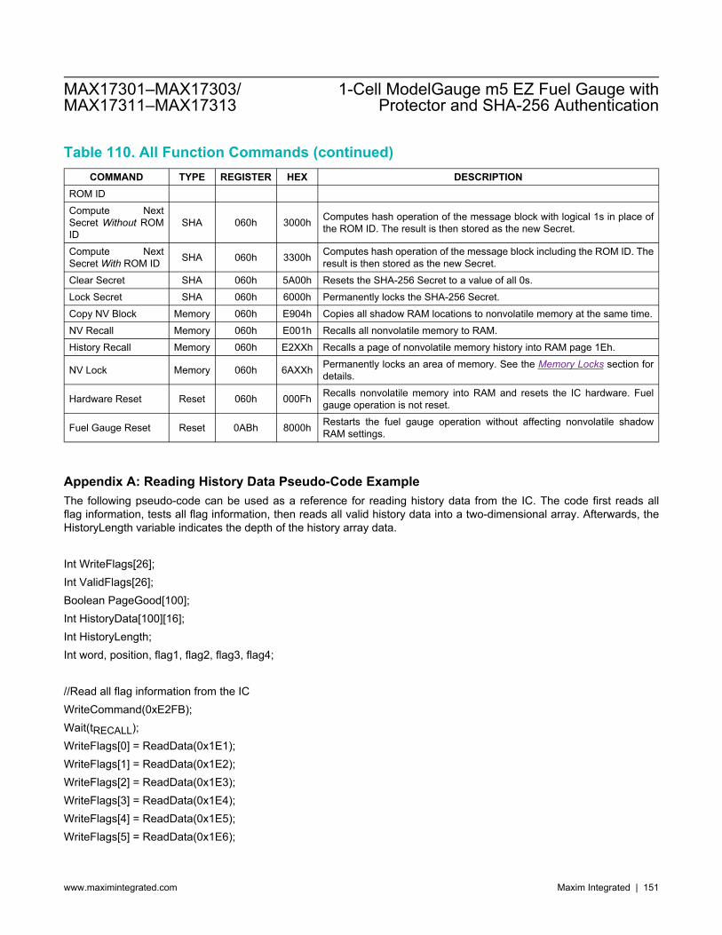
Table 110. All Function Commands (continued) COMMAND TYPE REGISTER HEX DESCRIPTION
ROM ID Compute Next Secret Without ROM ID
SHA 060h 3000h Computes hash operation of the message block with logical 1s in place of the ROM ID. The result is then stored as the new Secret.
Compute Next Secret With ROM ID SHA 060h 3300h Computes hash operation of the message block including the ROM ID. The
result is then stored as the new Secret. Clear Secret SHA 060h 5A00h Resets the SHA-256 Secret to a value of all 0s. Lock Secret SHA 060h 6000h Permanently locks the SHA-256 Secret. Copy NV Block Memory 060h E904h Copies all shadow RAM locations to nonvolatile memory at the same time. NV Recall Memory 060h E001h Recalls all nonvolatile memory to RAM. History Recall Memory 060h E2XXh Recalls a page of nonvolatile memory history into RAM page 1Eh.
NV Lock Memory 060h 6AXXh Permanently locks an area of memory. See the Memory Locks section for details.
Hardware Reset Reset 060h 000Fh Recalls nonvolatile memory into RAM and resets the IC hardware. Fuel gauge operation is not reset.
Fuel Gauge Reset Reset 0ABh 8000h Restarts the fuel gauge operation without affecting nonvolatile shadow RAM settings.
Appendix A: Reading History Data Pseudo-Code Example The following pseudo-code can be used as a reference for reading history data from the IC. The code first reads all flag information, tests all flag information, then reads all valid history data into a two-dimensional array. Afterwards, the HistoryLength variable indicates the depth of the history array data. Int WriteFlags[26]; Int ValidFlags[26]; Boolean PageGood[100]; Int HistoryData[100][16]; Int HistoryLength; Int word, position, flag1, flag2, flag3, flag4; //Read all flag information from the IC WriteCommand(0xE2FB); Wait(tRECALL); WriteFlags[0] = ReadData(0x1E1); WriteFlags[1] = ReadData(0x1E2); WriteFlags[2] = ReadData(0x1E3); WriteFlags[3] = ReadData(0x1E4); WriteFlags[4] = ReadData(0x1E5); WriteFlags[5] = ReadData(0x1E6);
MAX17301–MAX17303/MAX17311–MAX17313
1-Cell ModelGauge m5 EZ Fuel Gauge withProtector and SHA-256 Authentication
www.maximintegrated.com Maxim Integrated | 151

WriteFlags[6] = ReadData(0x1E7); WriteFlags[7] = ReadData(0x1E8); WriteFlags[8] = ReadData(0x1E9); WriteFlags[9] = ReadData(0x1EA); WriteFlags[10] = ReadData(0x1EB); WriteFlags[11] = ReadData(0x1EC); WriteFlags[12] = ReadData(0x1ED); WriteFlags[13] = ReadData(0x1EE); WriteFlags[14] = ReadData(0x1EF); WriteCommand(0xE2FC); Wait(tRECALL); WriteFlags[15] = ReadData(0x0E0); WriteFlags[16] = ReadData(0x0E1); WriteFlags[17] = ReadData(0x0E2); WriteFlags[18] = ReadData(0x0E3); WriteFlags[19] = ReadData(0x0E4); WriteFlags[20] = ReadData(0x0E5); WriteFlags[21] = ReadData(0x0E6); WriteFlags[22] = ReadData(0x0E7); WriteFlags[23] = ReadData(0x0E8); WriteFlags[24] = ReadData(0x0E9); WriteFlags[25] = ReadData(0x0EA); ValidFlags[0] = ReadData(0x0EB); ValidFlags[1] = ReadData(0x0EC); ValidFlags[2] = ReadData(0x0ED); ValidFlags[3] = ReadData(0x0EE); ValidFlags[4] = ReadData(0x0EF); WriteCommand(0xE2FD); Wait(tRECALL); ValidFlags[5] = ReadData(0x1E0); ValidFlags[6] = ReadData(0x1E1); ValidFlags[7] = ReadData(0x1E2); ValidFlags[8] = ReadData(0x1E3); ValidFlags[9] = ReadData(0x1E4); ValidFlags[10] = ReadData(0x1E5); ValidFlags[11] = ReadData(0x1E6); ValidFlags[12] = ReadData(0x1E7);
MAX17301–MAX17303/MAX17311–MAX17313
1-Cell ModelGauge m5 EZ Fuel Gauge withProtector and SHA-256 Authentication
www.maximintegrated.com Maxim Integrated | 152

ValidFlags[13] = ReadData(0x1E8); ValidFlags[14] = ReadData(0x1E9); ValidFlags[15] = ReadData(0x1EA); ValidFlags[16] = ReadData(0x1EB); ValidFlags[17] = ReadData(0x1EC); ValidFlags[18] = ReadData(0x1ED); ValidFlags[19] = ReadData(0x1EE); ValidFlags[20] = ReadData(0x1EF); WriteCommand(0xE2FE); Wait(tRECALL); ValidFlags[21] = ReadData(0x1E0); ValidFlags[22] = ReadData(0x1E1); ValidFlags[23] = ReadData(0x1E2); ValidFlags[24] = ReadData(0x1E3); ValidFlags[25] = ReadData(0x1E4); //Determine which history pages contain valid data For loop = 0 to 99 word = (int)( loop / 8 ); position = loop % 8 ; //remainder flag1 = (WriteFlags[word] >> position) & 0x0001; flag2 = (WriteFlags[word] >> (position+8)) & 0x0001; flag3 = (ValidFlags[word] >> position) & 0x0001; flag4 = (ValidFlags[word] >> (position+8)) & 0x0001; if (flag1 || flag2) && (flag3 || flag4) PageGood[loop] = True; else PageGood[loop] = False; //Read all the history data from the IC HistoryLength = 0; For loop = 0 to 99 if(PageGood[loop]) == TRUE
MAX17301–MAX17303/MAX17311–MAX17313
1-Cell ModelGauge m5 EZ Fuel Gauge withProtector and SHA-256 Authentication
www.maximintegrated.com Maxim Integrated | 153

SendCommand(0xE226 + loop); Wait(tRECALL); HistoryData[HistoryLength][0] = ReadData(0x1E0); ... HistoryData[HistoryLength][15] = ReadData(0x0EF); HistoryLength++;
MAX17301–MAX17303/MAX17311–MAX17313
1-Cell ModelGauge m5 EZ Fuel Gauge withProtector and SHA-256 Authentication
www.maximintegrated.com Maxim Integrated | 154

Typical Application Circuits
Typical Application Schematic
REG
CSNCSP
SENSERESISTOR
PK+
MAX1730xMAX1730xMAXMAX1731x1731x
SDA/DQSCL/OD
ALRT/PIO HOSTµP
BATTERY PACK SYSTEM
PK-
BATT0.1µF
N N0.1µF
CP CHG DIS
OPTIONALNTC THERMISTOR
0.47µF
ZVC
PCKP
TH
PFAIL (MAX173x1 ONLY)
Secondary Protector
10Ω
1kΩ
(TDFN)EP
OPTIONAL
(WLP)GND
0.1µF
MAX17301–MAX17303/MAX17311–MAX17313
1-Cell ModelGauge m5 EZ Fuel Gauge withProtector and SHA-256 Authentication
www.maximintegrated.com Maxim Integrated | 155

Typical Application Circuits (continued)
Typical Application with a Secondary Protector
REG
CSNCSP
SENSE RESISTOR
PK+
MAX1730xMAX1730xMAXMAX1731x1731x
SDA\DQSCL\OD
ALRT\PIO HOSTµP
BATTERY PACK SYSTEM
PK-
BATT
0.1µF
N
N
0.1µFCP
CHG DIS
OPTIONALNTC THERMISTOR
0.47µF
PCKP
TH
PFAIL
N
N
N N
VMDO COVSS
VDDCTL
0.1µF
0.1µF
R>1
MΩ
5R
33
0Ω
2kΩ
10kΩ
S-8230A
10Ω
0.1µF
1kΩ
ZVC
(WLP)GND
(TDFN)EP
When using the MAX1730x/MAX1731x with a secondary protector, there are a few instances that must be carefully considered so that the two protectors can work well together. In the event that the secondary protector trips first when there is an over charge protection event, the MAX1730x/MAX1731x is cut off from the battery voltage and it sees the charger voltage at the BATT pin which introduces error into the fuel gauge.
In the event of an over-discharge current or short-circuit current is detected by the secondary protector, it cuts off power to the MAX1730x/MAX1731x and cause the fuel gauge to reset and requires a charger to wake it back up. A good option would be to have a latch on the secondary protector to also require a charger to wake it up as well to allow both protectors to wake up at the same time.
MAX17301–MAX17303/MAX17311–MAX17313
1-Cell ModelGauge m5 EZ Fuel Gauge withProtector and SHA-256 Authentication
www.maximintegrated.com Maxim Integrated | 156

Typical Application Circuits (continued)
Typical Application with a Fuse
REG
CSNCSP
SENSE RESISTOR
PK+
MAX1730xMAX1730xMAXMAX1731x1731x
SDA\DQSCL\OD
ALRT\PIO HOSTµP
BATTERY PACK SYSTEM
PK-
BATT
0.1µF
N
N
0.1µFCP
CHG DIS
OPTIONALNTC THERMISTOR
0.47µF
PCKP
TH
PFAIL
3 TERMINAL FUSE
N
N
VM
CO
VSS
VDD0.1µF
33
0Ω
S-8206A
10Ω
0.1µF
1kΩ
ZVC
(WLP)GND
(TDFN)EP
The MAX1730x/MAX1731x can permanently open a three terminal fuse with the PFAIL pin when a permanent failure is detected.
Pushbutton Schematic
MAX1730xMAX1730xMAXMAX1731x1731x
SYSTEM INTERFACE
PMIC
N
SYSTEM AP
N N
CHG DIS
BATT
BUTTON
1.8V (VIO)
ALRT/PIO
OPTIONAL PULLUP
PUSH BUTTON
A pushbutton can be shared by the MAX1730x/MAX1731x and the system to wake up the system and the MAX1730x/MAX1731x.
MAX17301–MAX17303/MAX17311–MAX17313
1-Cell ModelGauge m5 EZ Fuel Gauge withProtector and SHA-256 Authentication
www.maximintegrated.com Maxim Integrated | 157

Typical Application Circuits (continued) The diode on the system interface PMIC blocks the pulldown when there is no supply. This prevents the wakeup for the MAX1730x/MAX1731x when the system interface PMIC loses power in ship mode. The diode on the ALRT/PIO pin prevents the alert pulldown from triggering a button action on the PMIC. This prevents accidental shutdown in the event of a alert uncleared for > 10 seconds. The FET between MAX1730x/MAX1731x and System AP is to block the System AP pulldown from triggering the wakeup when the AP doesn’t have power. The FET acts as a level shifter and passes the pulldown alert signal in both directions when the 1.8V voltage is present.
MAX17301–MAX17303/MAX17311–MAX17313
1-Cell ModelGauge m5 EZ Fuel Gauge withProtector and SHA-256 Authentication
www.maximintegrated.com Maxim Integrated | 158

Ordering Information
PART FUEL GAUGE PROTECTOR AUTHENTICATION INTERFACE PIN-PACKAGE
MAX17301 G+* 1-Cell Fuel Gauge with ModelGauge m5 EZ 2-Level SHA-256 I2 C 14 TDFN-
EP
MAX17301G+T* 1-Cell Fuel Gauge with ModelGauge m5 EZ 2-Level SHA-256 I 2 C 14 TDFN-
EP
MAX17301X+ 1-Cell Fuel Gauge with ModelGauge m5 EZ 2-Level SHA-256 I 2 C 15 WLP
MAX17301X+T 1-Cell Fuel Gauge with ModelGauge m5 EZ 2-Level SHA-256 I 2 C 15 WLP
MAX17311 G+* 1-Cell Fuel Gauge with ModelGauge m5 EZ 2-Level SHA-256 1-Wire 14 TDFN-
EP
MAX17311G+T* 1-Cell Fuel Gauge with ModelGauge m5 EZ 2-Level SHA-256 1-Wire 14 TDFN-
EP
MAX17311X+ 1-Cell Fuel Gauge with ModelGauge m5 EZ 2-Level SHA-256 1-Wire 15 WLP
MAX17311X+T 1-Cell Fuel Gauge with ModelGauge m5 EZ 2-Level SHA-256 1-Wire 15 WLP
MAX17302 G+* 1-Cell Fuel Gauge with ModelGauge m5 EZ 1-Level SHA-256 I 2 C 14 TDFN-
EP
MAX17302G+T* 1-Cell Fuel Gauge with ModelGauge m5 EZ 1-Level SHA-256 I 2 C 14 TDFN-
EP
MAX17302X+ 1-Cell Fuel Gauge with ModelGauge m5 EZ 1-Level SHA-256 I 2 C 15 WLP
MAX17302X+T 1-Cell Fuel Gauge with ModelGauge m5 EZ 1-Level SHA-256 I 2 C 15 WLP
MAX17312 G+* 1-Cell Fuel Gauge with ModelGauge m5 EZ 1-Level SHA-256 1-Wire 14 TDFN-
EP
MAX17312G+T* 1-Cell Fuel Gauge with ModelGauge m5 EZ 1-Level SHA-256 1-Wire 14 TDFN-
EP
MAX17312X+ 1-Cell Fuel Gauge with ModelGauge m5 EZ 1-Level SHA-256 1-Wire 15 WLP
MAX17312X+T 1-Cell Fuel Gauge with ModelGauge m5 EZ 1-Level SHA-256 1-Wire 15 WLP
MAX17303 G+* 1-Cell Fuel Gauge with ModelGauge m5 EZ 1-Level I 2 C 14 TDFN-
EP
MAX17303G+T* 1-Cell Fuel Gauge with ModelGauge m5 EZ 1-Level I 2 C 14 TDFN-
EP
MAX17303X+ 1-Cell Fuel Gauge with ModelGauge m5 EZ 1-Level I 2 C 15 WLP
MAX17303X+T 1-Cell Fuel Gauge with ModelGauge m5 EZ 1-Level I 2 C 15 WLP
MAX17313 G+* 1-Cell Fuel Gauge with ModelGauge m5 EZ 1-Level 1-Wire 14 TDFN-
EP
MAX17313G+T* 1-Cell Fuel Gauge with ModelGauge m5 EZ 1-Level 1-Wire 14 TDFN-
EP
MAX17313X+ 1-Cell Fuel Gauge with ModelGauge m5 1-Level 1-Wire 15 WLP
MAX17301–MAX17303/MAX17311–MAX17313
1-Cell ModelGauge m5 EZ Fuel Gauge withProtector and SHA-256 Authentication
www.maximintegrated.com Maxim Integrated | 159

PART FUEL GAUGE PROTECTOR AUTHENTICATION INTERFACE PIN-PACKAGE
EZ
MAX17313X+T 1-Cell Fuel Gauge with ModelGauge m5 EZ 1-Level 1-Wire 15 WLP
+Denotes a lead(Pb)-free/RoHS-compliant package. T = Tape and reel. *Future product—contact factory for availability.
MAX17301–MAX17303/MAX17311–MAX17313
1-Cell ModelGauge m5 EZ Fuel Gauge withProtector and SHA-256 Authentication
www.maximintegrated.com Maxim Integrated | 160

Revision History REVISION NUMBER
REVISION DATE DESCRIPTION PAGES
CHANGED 0 1/19 Initial release — 1 3/19 Updated the Ordering Information table 1, 157
2 4/19
Updated Typical Operating Characteristics, General Description, Protector, Modes of Operation, Power Mode Transition State Diagram, Cycles and nCycles Register, AgeForecast Register, Battery Life Logging, Determining Number of Valid Logging Entries, Nonvolatile Block Programming, nConfig Register, nPackCfg Register, Register Settings for Common Thermistor Types, Device Reset, and Appendix A: Reading History Data Pseudo-Code Example section; added 2-Stage MKDF Authentication Scheme and SOCHold Register section; updated Typical Application Circuits
1, 22, 23, 26–28, 32, 33,
41, 44, 45, 60–62, 70–160
3 5/19 Updated the Ordering Information table 1, 159, 160
For pricing, delivery, and ordering information, please visit Maxim Integrated’s online storefront at https://www.maximintegrated.com/en/storefront/storefront.html.
Maxim Integrated cannot assume responsibility for use of any circuitry other than circuitry entirely embodied in a Maxim Integrated product. No circuit patent licenses are implied. Maxim Integrated reserves the right to change the circuitry and specifications without notice at any time. The parametric values (min and max limits) shown in the Electrical Characteristics table are guaranteed. Other parametric values quoted in this data sheet are provided for guidance.
MAX17301–MAX17303/MAX17311–MAX17313
1-Cell ModelGauge m5 EZ Fuel Gauge withProtector and SHA-256 Authentication
Maxim Integrated and the Maxim Integrated logo are trademarks of Maxim Integrated Products, Inc. © 2019 Maxim Integrated Products, Inc.