heterojunction diodes including zno thin films thesis work consists of the characterization of two...
TRANSCRIPT

1
Heterojunction diodes including ZnO thin films
Ângelo Miguel Alfaia de Andrade Castelinho Department of Physics of IST, Lisbon (Portugal)
(Dated: April 2013)
Abstract
This thesis work consists of the characterization of two semiconductor materials and the junction as a diode. These materials are Zinc Oxide (ZnO) and Gallium Nitride (GaN). The n-type ZnO films are produced in our laboratory by Pulsed Laser Deposition (PLD). On the other hand, GaN is given to us by research groups from EPFL, Switzerland, and RPI, USA. A series of ZnO films was deposited to study their optical and physical properties by varying the oxygen pressure. For p-type GaN we studied two metal contacts, which are: Aluminum and Nickel/Gold. Rapid thermal annealing (RTA) was needed to activate the Mg dopants.
The characterization of these materials consists of the following methods: I-V measurement to study their resistivity and carrier density; X-Ray Diffraction to study the structure of the material and to compare results with literature; SEM images to compare the surface of each sample; Optical Transmittance to study their optical properties and their band gaps.
The metal contacts for I-V characterization were done by Thermal Evaporation. For GaN again RTA was used to avoid formation of Schottky barrier contacts. Different metals are chosen for good ohmic contacts on ZnO and GaN.
Finally, diodes are made by deposition of n-type ZnO on top of p-type GaN by PLD. To analyze the diodes we performed I-V measurements and analyzed their ideality factor, leakage current and series resistance.
Keywords: Diode, ZnO, GaN, PLD, Resistivity, Electronic Density, Schottky Barrier, Ohmic Contact.
1. Introduction
Contemporary day life relies heavily on
modern technology, such as semiconductor-based electronics. An example of this fact is the use of LEDs, light-emitting devices, in various applications. Recently, in this type of equipment, the color range could effectively be extended to the blue and violet spectrum with the availability of high-quality wide-band-gap semiconductors like GaN. Accordingly, the present work is based on the preparation and characterization of a heterojunction diode with GaN and ZnO. Various characterization methods on the micrometer and nanometer scale are employed to study the morphology and the electronic properties of GaN and ZnO thin films. The latter were prepared during the course of this work by pulsed laser deposition system.
The characteristic of a ZnO-on-GaN heterostructure has already been studied by various research groups. In our case, we have use pulsed laser deposition (PLD) for the production of the ZnO thin film, whereas most of the GaN layers were grown by MOCVD at EPFL, Lausanne. Such heterojunctions will be important for the development of optoelectronic device such as blue and ultraviolet LEDs.
This project consists of 6 chapters, including this introduction. In Chapter 2, “Literature Review”, we introduce the theoretical part of my work, subdivided into the topics on isolated semiconductors, "pn" junctions, metallic contacts and the materials that we used in this work. In Chapter 3 we present the techniques used to deposit materials and to improve them. Details are given for Pulsed Laser Deposition (PLD), Thermal Evaporation and Metal-organic Chemical Vapor Deposition (MOCVD), which are relevant deposition techniques for our samples. To improve the conductivity of the p-type GaN layers, the used technique was Rapid Thermal Annealing (RTA). Chapter 4 introduces the methods that characterize the morphological, optical, and electrical properties of the materials we employed. In Chapter 5 we present the results and discuss them according to both literature reports and theoretical aspects from previous chapters. Firstly we will study the materials individually, ZnO and GaN, and after that we compare the different aspects concerning the metal contact, like the Schottky barrier type or ohmic contacts. Finally, we will discuss the I-V characteristics of the diodes we produced. Chapter 6 closes the report with a summary and suggestions for future work.
2
2. Literature Review
2.1 Semiconductors Layers In this section we present a summary about
Semiconductor layers and junctions. To do the summary we used five Ref. [1-5].
There are two bands that are separated by regions of energy that the electrons in the solid cannot possess, in what is called a forbidden gap. The highest energy band that is completely filled by electrons at 0K is called the “valence band”. The next higher energy band, separated from the valence band by the forbidden gap, is called the “conduction band”.
The electron density in the conduction band is “ ”, and the hole density in the valence band is “ ”.
The type of material depends on the density of donpants . The atoms that tend to have free electron after forming covalent bands are “donors”. On the other hand, the atoms that need an electron valence band left a free hole are “acceptors”. The donors form an n-type and acceptors form a p-type.
The resistivity, ρn, for n-type is defined by:
(1),
Where, is the electron charge, electron
mobility. For p-type the definition is the same, but
instead of we have . The mobility is for holes and
not for electron. For a uniform conductor with length L, width
W, and thickness t (Figure 1), its resistance R is given by:
(2), So, the resistivity can be also
(3)
Figure 1 Dimensions t, W, L
Its sheet resistance (Ω/sq) is calculated by:
(4) so the resistance as a function of sheet
resistance is: (5).
2.2 p-n Junction A diode is basically a p-n junction, it consists
of p-type semiconductor material brought into close contact with n-type semiconductor. There are two types of structures. Homostructures, which n-type
and p-type are the same material but the doping is different. On the other hand there are also heterostructures, where n-type and p-type layers are made of different materials.
In general, the positive pole of the power supply is connected to a p-side of the junction. When V=0 we are in thermal equilibrium, but when V>0 we are in forward bias, and on the other hand V<0 means reverse bias. The diffusion current in forward bias is higher than in thermal equilibrium because the barrier is lower and more electrons from the n-type layer can diffuse to the p-type side. Similarly, more holes in p-type diffuse from the "p" to the "n" side. On the other hand, for reverse bias, the barrier is obviously higher, so diffusion is usually negligible. The drift current is relatively insensitive to the height of the potential barrier.
An applied forward bias increases the probability that a carrier can diffuse across the junction by the factor exp(qVf/kT). The same occurs in reverse bias, since the equilibrium current is equal to “I0”. Accordingly, the total current is given by the Shockley equation:
(6),
where is the ideality factor. It varies
between 1 and 2, depending on the presence of carrier generation via defects in the junction region.
2.3 Metal-Semiconductor Junctions To study the properties of semiconductors,
like I-V curves, or to measure the conductivity, we put metal in contact above the thin film. When a barrier is formed this way it is called Schottky Barrier, but if there is no barrier we have an ohmic contact. When a semiconductor with work function energy is brought in contact with a metal,
charge transfer occurs until the Fermi levels are aligned at equilibrium. A Schottky Barrier forms when , for a n-type semiconductor. On the
other hand for p-type material a barrier appears when . An ideal metal-semiconductor
contact is called ohmic contact, when we have a linear I-V characteristic in both bias directions. It occurs when for n-type and for p-
type. 2.4 Heterojunctions A heterojunction is a junction between two
different semiconductors with dissimilar Eg. When we bring two semiconductors with different Eg, work functions and electron affinities into contact, we expect a discontinuity in the energy bands in the

3
thermal equilibrium. The difference between valence bands is ∆Ev, and ∆Ec for conduction bands. In an ideal case, ∆Ec would be the difference between electron affinities q(χ2-χ1) and ∆Ev the difference ∆Eg-∆Ec.
2.5 Materials Used The principal materials used in this work were
n-ZnO and p-GaN. The n-ZnO was produced in our laboratory by Pulsed Laser Deposition (PLD). The GaN films were supplied by the group of Nicolas Grandjean and Jean-Francois Carlin from EPFL in Lausanne. They used MOCVD for the deposition of Mg-doped GaN films on sapphire substrates.
Nowadays, however, ZnO is seen by the scientific community as a “future material” [6]. The ZnO crystallizes in two main structures, which can be a cubic zinc-blende or hexagonal wurtzite. The structure of ZnO deposited by PLD is wurtzite. ZnO is a n-type semiconductor with a direct band gap of 3.3 eV [7-9]. The electron concentration with the resistivity calculated for each sample. The electron mobility varies with electron density, in our work we used, [6].
Gallium nitride belongs to the group of III-V. GaN can have 2 structures, wurtzite or zinc-blende, as ZnO. It has a direct band gap of a 3.4 eV at room temperature [10-12]. We calculated the electron concentration from its resistivity. The mobility used in this calculation was [13].
2.6 Diode n-ZnO/p-GaN The diode p-GaN/n-ZnO was been studied by
many research groups [12,14]. They did two types of diode: pn junction and a pin junction. The pin heterostructures are usually realized to study LEDs. In our work we studied the I-V characteristic of this type of diode.
3. Deposition and Process Techniques
3.1 Pulsed Laser Deposition (PLD) In general, the idea of PLD is simple. A
pulsed laser beam is focused onto the surface of a solid target and the strong absorption of the electromagnetic radiation leads to rapid evaporation of the target materials. This evaporated material consists of excited and ionized species, which form a plasma plume on the surface of the target and deposit on a substrate as a thin film (Figure 2).
In our project, the laser used was a Nd:YAG which could be operated at three wavelengths, one of 266 nm (UV), one of 532nm (visible) and another of 1064nm (IR). For the purpose of this project, we
used the UV wavelength due to the smaller diameter of the deposited particles.
Figure 2 PLD Chamber
There are four different steps in the process of the PLD:
• Laser radiation interacts with the target; • Laser ablation and creation of plasma
plume; • Deposition of the material on substrate; • Nucleation and growth of thin film on the
substrate surface; The main advantages to use PLD are: • The deposition can be realized at low
temperature [7]; • There is a wide range of material that PLD
can deposit, like oxides, metals, semiconductors, and even polymers [7];
• The deposition is cleaner and is cheaper compared to Chemical Vapor Deposition [7].
The main disadvantages are: • The plasma plume cross section is small, so
it creates a limitation in the size of the sample [7].
• There is an intrinsic “splashing” due to the laser ablation, which produces big particles from the target material in the sample [7].
• 3.2 Thermal Evaporation This process is very simple: we put a metal in
a basket (or boat) near to the substrate. The metal heats up until it evaporates and finally condenses on the substrate. Evaporation is made in vacuum.
3.3 Metal Organic Chemical Vapor
Deposition (MOCVD) This technique was used by J.F. Carlin to
deposit GaN onto sapphire wafers. However, this process is very complex to grow crystalline layers. As the method's name states, this is a chemical process that consists in a source of gas mixture needed for growth, and if necessary for doping, which is passed over a heated substrate. This

4
passage then leaves the atoms on the surface and these crystallized atoms create a new crystalline layer. MOCVD can deposit a few microns per hour. Additionally, the quality of the produced layers is very good and it can work at high temperatures. However, this is an expensive method and demands the handling of toxic gases.
3.4 Rapid Thermal Anneal (RTA) Rapid thermal annealing is a process used in
the fabrication of semiconductor devices which consists in heating a sample at the temperature we want. The variation of the temperature can be controlled. This rapid variation affects the electrical and structural properties of the sample. To accomplish this, the process was done at the ITN infrastructure with the collaboration of Dr. Eduardo Alves and Dr. Norberto Catarino.
4. Characterization Techniques
4.1 X-Ray Diffraction (XRD) X-ray diffraction (XRD) is a versatile non-
destructive technique, that reveals detailed information about the chemical composition and crystallographic structure. The source of X-ray beam focuses the sample using an X-ray tube. This sweeps all θ, and the reflected beams are collected by a detector that converts this received beam in counts. The wavelength of X-ray is 1.54 Å.
4.2 Scanning Electron Microscopic (SEM) This technique uses a focused beam of high-
energy electrons to generate a variety of signals at the surface that we want to study. This signal gives us information about the sample including external morphology, chemical composition, and crystalline structure.
4.3 Transmittance Optical Transmittance is a technique used to
measure the energy gap of semiconductor. It consists of measuring the absorption of the incident photons by the material. The photons with energies greater than Eg of the semiconductor are absorbed, while photons with energies lower than the band gap are transmitted. The intensity of the incident beam (I0) after crossing the sample divides itself in three intensities, which are; transmitted (IT), absorbed (IA) and reflected (IR) [7]. So:
(7)
The intensity of transmitted light through the sample is given by Beer’s equation: (8),
where α is the absorption coefficient (cm-1) and t the thickness of the sample.
The Energy gap is calculated by the α depending on the photon energy. . We traced a straight line from middle height of the abrupt increase until x-axis. This value of x-axis is the energy gap. [1]
The Tauc plot is another method to determine the energy gap of a sample. The square root of the product between absorption coefficient and photon energy is plotted, depending on the photon
energy. To measure the Band gap, we trace a line which is the slope of the abrupt increase onto the x-axis. This value is the band gap [15].
4.4 I-V Characterization I-V characterization consists basically on
applying a voltage between two probes on the sample and measuring the current that flows through the sample (Figure 3). To do the characterization we used a computer program which applies a voltage sweep up to maximum desired voltage.
Figure 3 Circuit schematic of I-V measurement.
This characterization was essential in our work, because it enabled us to study the resistivity of each sample that we used. It also allowed the characterization of each diode that we produced.
5. Results and Discussion
5.1 ZnO We used PLD to deposit the n-ZnO on a BK7
substrate to find the best depostion parameters for a diode. In a series of depositions we changed the oxygen pressure. The target used was ZnO powder, which was dense and compac. We needed a good conductive thin film with high density of electrons. According to the literature on the subject [16], resistivity increases with deposition temperature. The temperature that we chose was 350ºC because we wanted a low resistivity. We could have used room temperature, but the resistivity would have been too low and the ZnO would almost be a conductor material. The parameters of deposition were: Temperature was 350ºC; time of deposition was 120 minutes; the laser wavelength λ of the laser was 266 nm; the laser frequency was 10Hz; the focus length

5
was 22 cm. We deposited six samples, the oxygen pressure was: 0.00mbar (ZnO127), 0.02mbar (ZnO123), 0.04mbar (ZnO124), 0.06mbar (ZnO125), 0.08mbar (ZnO126) and 0.10 mbar (ZnO128). XRD gave us the structure of ZnO. The expected peak of XRD was 34.50, which corresponds to the (002) plane of wurtzite structure [17-18]. The FWHM gives us the quality of the film, which means that the lower the FWHM the better the quality of the sample (Figure 4).
Figure 4 XRD for ZnO samples
The peak positions of our samples were close to the literature values [32]. The FWHM was quite large, the worst thin film was ZnO 124. We can correlate this result later on SEM images.
The transmittance allows the study of the band gap for the ZnO. The next plot shows the transmittance for ZnO 126 (Figure 5).
Figure 5 Transmittance curve for ZnO 126
The Tauc plot gave us the band gap of ZnO 126 (Figure 6), which was 3.27 eV.
Figure 6 Tauc plot of each Sample
We did this analysis for all samples. Their band gaps are shown in next plot (Figure 7).
Figure 7 Band Gap of each Sample of ZnO.
The surface of samples was analyzed by SEM. To see the surface in detail we show the picture with 50000x amplification (Figure 8).
Figure 8 a) ZnO 127 at 50000x, b) ZnO 124 at 50000x
The size of particles in a) was the same (30 nm). When oxygen was introduced in the chamber, their size decreased (to 20 nm), but there were other particles with bigger size (50 nm to 70 nm). In b) we could see “islands”, so, as we said previously on XRD, the quality of the ZnO 124 was worse than the others.
We expected that physical properties like resistivity and electron density changed with the variation of oxygen pressure, because this element was the one that controlled the doping. First we measured the resistance of each sample by means of I-V characterization. The metal used for the contacts was Al. The thickness of the samples was
6
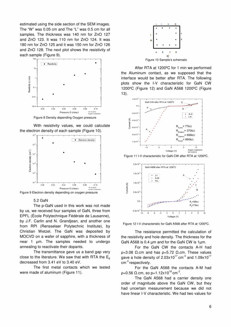
estimated using the side section of the SEM images. The “W” was 0.05 cm and The “L” was 0.5 cm for all samples. The thickness was 140 nm for ZnO 127 and ZnO 123. It was 110 nm for ZnO 124. It was 180 nm for ZnO 125 and it was 150 nm for ZnO 126 and ZnO 128. The next plot shows the resistivity of each sample (Figure 9).
Figure 8 Density depending Oxygen pressure
With resistivity values, we could calculate the electron density of each sample (Figure 10).
Figure 9 Electron density depending on oxygen pressure
5.2 GaN The p-GaN used in this work was not made
by us, we received four samples of GaN, three from EPFL (École Polytechnique Fédérale de Lausanne), by J.F. Carlin and N. Grandjean, and another one from RPI (Rensselaer Polytechnic Institute), by Christian Wetzel. The GaN was deposited by MOCVD on a wafer of sapphire, with a thickness of near 1 µm. The samples needed to undergo annealing to reactivate their dopants.
The transmittance gave us a band gap very close to the literature. We saw that with RTA the Eg decreased from 3.41 eV to 3.40 eV.
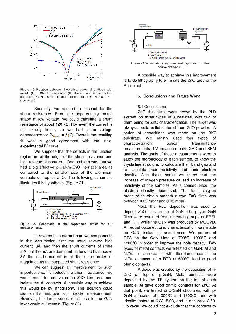
The first metal contacts which we tested were made of aluminum (Figure 11).
Figure 10 Sample’s schematic
After RTA at 1200ºC for 1 min we performed the Aluminum contact, as we supposed that the interface would be better after RTA. The following plots show the I-V characteristic for GaN CW 1200ºC (Figure 12) and GaN A568 1200ºC (Figure 13).
Figure 11 I-V characteristic for GaN CW after RTA at 1200ºC.
Figure 12 I-V characteristic for GaN A568 after RTA at 1200ºC.
The resistance permitted the calculation of the resistivity and hole density. The thickness for the GaN A568 is 0.4 µm and for the GaN CW is 1µm.
For the GaN CW the contacts A-H had ρ=3.08 Ω.cm and has ρ=5.72 Ω.cm. These values gave a hole density of 2.03x1017 cm-3 and 1.09x1017 cm-3 respectively.
For the GaN A568 the contacts A-M had ρ=0.56 Ω.cm, so p=1.12x1018 cm-3.
The GaN A568 had a carrier density one order of magnitude above the GaN CW, but they had uncertain measurement because we did not have linear I-V characteristic. We had two values for

7
resistance in the same I-V characteristic because of this uncertainty.
The treatment of the next samples was different from these last two. They had Ni/Au contacts which were perfectly ohmic [19-20]. They suffered two RTAs: one at 700ºC for 5 minutes to reactivate the Mg dopants, and a second one at 600ºC for 5 minutes to reduce the unintentional barrier at the interface [21].
The next plot shows the I-V characteristic for GaN c007 and GaN c013 (Figure 14).
Figure 13 I-V characteristic of GaN c007b-2a
For these samples we had linear I-V characteristics, so the Ni/Au was a very good contact for GaN. The resulting carrier density of GaN c007b was ρ=0.96 Ω.cm, so p=6.49x1017 cm-3. For the GaN c013b was ρ=2.01 Ω.cm, so p=3.11x1017 cm-3.
With respect to XRD data, according to the literature [22-24], the gallium nitride had a peak at 34.5º, which corresponds to a (002) plane of wurtzite, like ZnO, and Sapphire had a peak at 42º that corresponds to a (006) plane.
Figure 14 XRD for GaN C-013b with and without RTA.
Before RTA we had a peak at 53.1º, which disappeared after the process. However, another peak appeared at 31.2º after the heating (Figure 15). The point at 53.1º was probably an impurity,
which after RTA disappeared. The 31.2º peak was believed to be another orientation of the GaN, like (100) plane, as Zervos et al. and R. Flauta et al.[23-24] showed in their work.
To see the difference between the layers of GaN c013 before and after RTA we used SEM. We used the amplification at 100000x. There were not any differences between layers.
5.3 Diode p-GaN/n-ZnO In this paragraph we analyzed the I-V
characteristic and we calculated its ideality factor, .
As the current in a diode is exponential, the analysis of I-V characteristic on a semi-log scale give a straight line, and the slope “ ” of this line
is , so the ideality factot .
The diode was p-GaN CW(1200º)/n-ZnO (Figure 16). For the characterization of n-ZnO 132 alone, deposition was done simultaneously on a Corning 7059 glass substrate. The analysis gave us Eg= 3.27 eV, ρ = 0.041 Ωcm and electron density was 7.62x1017cm3.
Figure 15 Semi-log I-V characteristic for p-GaN CW/n-ZnO B-2
contacts
The plot only showed a straight line at small voltage. The reason for this behavior is that for high voltage the protecting series resistance and the resistance of each surface. The ideality factor for this diode was .
The following plot shows the semi-log I-V characteristic for p-GaN A568(1200º)/n-ZnO (Figure 17).

8
Figure 16 Semi-log I-V for diode p-GaN A568(1200ºC)/n-ZnO, was
done abs for current to see forward and reserve current.
The n-ZnO 133 deposited had a Eg= 3.27 eV, ρ = 0.042 Ωcm and electron density was 7.25x1017cm3. This semi-log I-V characteristic appeared to be better than the first one, as the slope of the straight line gave us an ideality factor of . This
value was definitely a good value. We could not forget that the contact for the GaN was not ohmic. So this characteristic could be a rectifying contact from one of the metal-semiconductor interfaces, that might form a Schottky barrier. Such Schottky barrier contacts obey the same I-V equation as a pn junction, eq 6.
The following diode was procuded on top of p-GaN c007b-2a that had Ni/Au ohmic contacts. Here we performed pin diode. The n-ZnO 135 deposited had Eg= 3.26 eV, ρ = 0.045 Ωcm, so
6.94x1017cm3.
The following plot shows the semi-log I-V for this diode.
Figure 17 Semi-log I-V for diode M-1 (p-GaN c007b-2a/i-ZnO/n-
ZnO), was done abs for current to see forward and reserve current.
We needed to correct the IV curves for the series resistance, due to both the series resistance of the GaN film and the protecting 1kΩ resistor. The
potential drop in each resistance was considerable. The IV curves seem to be deformed with respect to ideal IV curves due to the presence of leakage currents. Those might originate from the impurity of the interface. The calculation of the ideality factor gave us a value of 30 for GaN c007b-2a M-1.
This value was much higher than 1. After that we executed another deposition
without an additional intrinsic layer on top of p-GaN c007b-1a. The n-ZnO 136 deposited had a Eg= 3.27 eV. ρ = 0.657 Ωcm, 4.76x1016cm3. As we could
see the electron density was one order of magnitude above the n-ZnO 135.
Next plot shows the semi-log I-V characteristic (Figure 19).
Figure 18 Semi-log I-V for diode B-1 (p-GaN c007b-1a/n-ZnO), was done abs for current to see forward and reserve current.
The ideality factor for this diode was 44, which was much higher than 1 or 2 as in an
ideal diode. The ratio between forward current and reverse current at the highest voltage levels was 10. However, we measured similar current levels for low voltages, for example between -3V and 3V. This strongly suggests that we need to consider a shunt resistance parallel to the p-n junction. A possibility for this to have happened was that, in the beginning of the deposition, the pressure oxygen was lower than ZnO135, so the particles in the plasma plume had more energy. These arriving particles might have damaged the GaN layer, creating interdiffusion of Ga, Zn or gas atoms like N or O within the interface region.
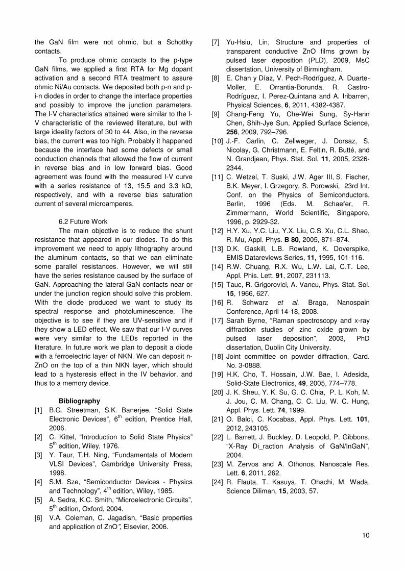
Firstly, we used a numerical fit for the diode IV characteristic to analyze the effect of the series resistance of approximately 13 kΩ (Figure 20).
9
Figure 19 Relation between theoretical curve of a diode with m=44 (Fit), Shunt resistance (R shunt), our diode before correction (GaN c007a b-1) and after correction (GaN c007a B-1 Corrected)
Secondly, we needed to account for the shunt resistance. From the apparent symmetric shape at low voltage, we could calculate a shunt resistance of about 120 kΩ. However, the current is not exactly linear, so we had some voltage dependence for . Overall, the resulting
fit was in good agreement with the initial experimental IV curve.
We suppose that the defects in the junction region are at the origin of the shunt resistance and high reverse bias current. One problem was that we had a big effective p-GaN/n-ZnO interface area as compared to the smaller size of the aluminum contacts on top of ZnO. The following schematic illustrates this hypothesis (Figure 21).
Figure 20 Schematic of the hypothesis circuit for our measurements.
In reverse bias current has two components in this assumption, first the usual reverse bias current, µA, and then the shunt currents of some mA, but the mA are dominant. In forward bias above 3V the diode current is of the same order of magnitude as the supposed shunt resistance.
We can suggest an improvement for such imperfections: To reduce the shunt resistance, we would need to remove some ZnO film area and isolate the Al contacts. A possible way to achieve this would be by lithography. This solution could significantly improve our diode measurement. However, the large series resistance in the GaN layer would still remain (Figure 22).
Figure 21 Schematic of improvement hypothesis for the
equivalent circuit.
A possible way to achieve this improvement is to do lithography to eliminate the ZnO around the Al contact.
6. Conclusions and Future Work
6.1 Conclusions ZnO thin films were grown by the PLD
system on three types of substrates, with two of them being for ZnO characterization. The target was always a solid pellet sintered from ZnO powder. A series of depositions was made on the BK7 substrate. We mainly used four types of characterization: optical transmittance measurements, I-V measurements, XRD and SEM analysis. The goals of these measurements were to study the morphology of each sample, to know the crystalline structure, to calculate their band gap and to calculate their resistivity and their electron density. With these series we found that the increase of oxygen pressure caused an increase of resistivity of the samples. As a consequence, the electron density decreased. The ideal oxygen pressure to obtain smooth n-type ZnO films was between 0.02 mbar and 0.03 mbar.
Next, the PLD deposition was used to deposit ZnO films on top of GaN. The p-type GaN films were obtained from research groups at EPFL and RPI, while the GaN was produced by MOCVD. An equal optoelectronic characterization was made for GaN, including transmittance. We performed RTA on the GaN films at 700ºC, 1000ºC and 1200ºC in order to improve the hole density. Two types of metal contacts were tested on GaN: Al and Ni/Au. In accordance with literature reports, the Ni/Au contacts, after RTA at 600ºC, lead to good ohmic contacts.
A diode was created by the deposition of n-ZnO on top of p-GaN. Metal contacts were deposited by the TE system on the top of each sample. Al gave good ohmic contacts for ZnO. At that point, we tested ZnO/GaN structures, with p-GaN annealed at 1000ºC and 1200ºC, and with ideality factors of 6.23, 5.98, and in one case 2.50. However, we could not exclude that the contacts to
10
the GaN film were not ohmic, but a Schottky contacts.
To produce ohmic contacts to the p-type GaN films, we applied a first RTA for Mg dopant activation and a second RTA treatment to assure ohmic Ni/Au contacts. We deposited both p-n and p-i-n diodes in order to change the interface properties and possibly to improve the junction parameters. The I-V characteristics attained were similar to the I-V characteristic of the reviewed literature, but with large ideality factors of 30 to 44. Also, in the reverse bias, the current was too high. Probably it happened because the interface had some defects or small conduction channels that allowed the flow of current in reverse bias and in low forward bias. Good agreement was found with the measured I-V curve with a series resistance of 13, 15.5 and 3.3 kΩ, respectively, and with a reverse bias saturation current of several microamperes.
6.2 Future Work The main objective is to reduce the shunt
resistance that appeared in our diodes. To do this improvement we need to apply lithography around the aluminum contacts, so that we can eliminate some parallel resistances. However, we will still have the series resistance caused by the surface of GaN. Approaching the lateral GaN contacts near or under the junction region should solve this problem. With the diode produced we want to study its spectral response and photoluminescence. The objective is to see if they are UV-sensitive and if they show a LED effect. We saw that our I-V curves were very similar to the LEDs reported in the literature. In future work we plan to deposit a diode with a ferroelectric layer of NKN. We can deposit n-ZnO on the top of a thin NKN layer, which should lead to a hysteresis effect in the IV behavior, and thus to a memory device.
Bibliography
[1] B.G. Streetman, S.K. Banerjee, “Solid State Electronic Devices”, 6th edition, Prentice Hall, 2006.
[2] C. Kittel, “Introduction to Solid State Physics” 5th edition, Wiley, 1976.
[3] Y. Taur, T.H. Ning, “Fundamentals of Modern VLSI Devices”, Cambridge University Press, 1998.
[4] S.M. Sze, “Semiconductor Devices - Physics and Technology”, 4th edition, Wiley, 1985.
[5] A. Sedra, K.C. Smith, “Microelectronic Circuits”, 5th edition, Oxford, 2004.
[6] V.A. Coleman, C. Jagadish, “Basic properties and application of ZnO”, Elsevier, 2006.
[7] Yu‐Hsiu, Lin, Structure and properties of transparent conductive ZnO films grown by pulsed laser deposition (PLD), 2009, MsC dissertation, University of Birmingham.
[8] E. Chan y Díaz, V. Pech-Rodríguez, A. Duarte-
Moller, E. Orrantia-Borunda, R. Castro- Rodríguez, I. Perez-Quintana and A. Iribarren, Physical Sciences, 6, 2011, 4382-4387.
[9] Chang-Feng Yu, Che-Wei Sung, Sy-Hann Chen, Shih-Jye Sun, Applied Surface Science, 256, 2009, 792–796.
[10] J.-F. Carlin, C. Zellweger, J. Dorsaz, S. Nicolay, G. Christmann, E. Feltin, R. Butté, and N. Grandjean, Phys. Stat. Sol, 11, 2005, 2326-2344.
[11] C. Wetzel, T. Suski, J.W. Ager III, S. Fischer, B.K. Meyer, I. Grzegory, S. Porowski, 23rd Int. Conf. on the Physics of Semiconductors, Berlin, 1996 (Eds. M. Schaefer, R. Zimmermann, World Scientific, Singapore, 1996, p. 2929-32.
[12] H.Y. Xu, Y.C. Liu, Y.X. Liu, C.S. Xu, C.L. Shao, R. Mu, Appl. Phys. B 80, 2005, 871–874.
[13] D.K. Gaskill, L.B. Rowland, K. Doverspike, EMIS Datareviews Series, 11, 1995, 101-116.
[14] R.W. Chuang, R.X. Wu, L.W. Lai, C.T. Lee, Appl. Phis. Lett. 91, 2007, 231113.
[15] Tauc, R. Grigorovici, A. Vancu, Phys. Stat. Sol. 15, 1966, 627.
[16] R. Schwarz et al. Braga, Nanospain Conference, April 14-18, 2008.
[17] Sarah Byrne, “Raman spectroscopy and x-ray diffraction studies of zinc oxide grown by pulsed laser deposition”, 2003, PhD dissertation, Dublin City University.
[18] Joint committee on powder diffraction, Card. No. 3-0888.
[19] H.K. Cho, T. Hossain, J.W. Bae, I. Adesida, Solid-State Electronics, 49, 2005, 774–778.
[20] J. K. Sheu, Y. K. Su, G. C. Chia, P. L. Koh, M. J. Jou, C. M. Chang, C. C. Liu, W. C. Hung, Appl. Phys. Lett. 74, 1999.
[21] O. Balci, C. Kocabas, Appl. Phys. Lett. 101, 2012, 243105.
[22] L. Barrett, J. Buckley, D. Leopold, P. Gibbons, “X-Ray Di_raction Analysis of GaN/InGaN”, 2004.
[23] M. Zervos and A. Othonos, Nanoscale Res. Lett. 6, 2011, 262.
[24] R. Flauta, T. Kasuya, T. Ohachi, M. Wada, Science Diliman, 15, 2003, 57.