high current connectors for board-to-fpc/for board-to
TRANSCRIPT

ACCTB112E 202110Panasonic Corporation 2021
FEATURESCapable of MAX. 5 A for power Rated current 1 A/pin (for power) 0.5 A/pin (for signal), Total: Max. 12 AAny terminal can be applied for power terminalLow contact resistance: Max. 40 mΩHigh speed transmission of 10 Gbps is available
Realized space savings for power line, and increased design flexibilityP4SP (0.4 mm pitch)
High Current Connectors For board-to-FPC/For board-to-board
TYPICAL APPLICATIONSDSC, mobile devices and industrial equipment
3.6mm 2.35mm HeaderSocket
DETAILS FEATURES
Reduce the number of pins for power line Increased design freedomAny pin contact can be used as a power contact. Any layout is possible for the power supply line.
Sample pin layout Total power: Max. 5 A (1 A/pin × 10 pins)
ORDERING INFORMATION (PART NO.)
Rated current value 1 A/pinFor power terminal For signal terminal
1 A/pin x 10 pins 0.5 A/pinTotal: Max. 12 A
5A
5A
Max. 0.3A/pin
Max. 0.3A/pinMax. 0.5A/pin
Max. 0.5A/pin
5A
5A
Spacereduction
Previousproduct
P4SP
Power line (5A): 0.3A × 34 pins
Power line (5A): 1A × 10 pins
24 pinsreduced24 pinsreduced
5A 2A
1A1A 1A 1A
1A 1A 2A
5A
Number of pins (2 digits)
Mated height(Socket)1: 1.5 mm2: 2.5 and 3.0mm(Header)1: 1.5 and 2.5mm3: 3.0mm
AXF 1 2
5G: Socket6G: Header
industrial.panasonic.com/ac/e/2021.10 ー 1 ー

High Current Connectors P4SP (0.4 mm pitch)
Panasonic Corporation Electromechanical Control Business Divisionindustrial.panasonic.com/ac/e/ ACCTB112E 202110Panasonic Corporation 2021
PRODUCT TYPES
Mated height Number of pins
Part No. Standard packingSocket Header Inner carton (1-reel) Outer carton
1.5 mm
10 AXF5G1012 AXF6G1012
3,000 pcs. 6,000 pcs.
16 AXF5G1612 AXF6G161220 AXF5G2012 AXF6G201224 AXF5G2412 AXF6G241226 AXF5G2612 AXF6G261230 AXF5G3012 AXF6G301234 AXF5G3412 AXF6G341238 AXF5G3812 AXF6G381240 AXF5G4012 AXF6G401250 AXF5G5012 AXF6G501260 AXF5G6012 AXF6G601270 AXF5G7012 AXF6G701280 AXF5G8012 AXF6G801290 AXF5G9012 AXF6G9012
100 AXF5G0012 AXF6G0012
2.5 mm
20 AXF5G2022 AXF6G201230 AXF5G3022 AXF6G301240 AXF5G4022 AXF6G401260 AXF5G6022 AXF6G601280 AXF5G8022 AXF6G8012
100 AXF5G0022 AXF6G0012
3.0 mm
20 AXF5G2022 AXF6G203230 AXF5G3022 AXF6G303260 AXF5G6022 AXF6G603280 AXF5G8022 AXF6G8032
100 AXF5G0022 AXF6G0032Notes: 1. Order unit: For volume production: 1-inner carton (1-reel) units. For samples, please contact our sales representative.
2. Please contact our sales representative for connectors having a number of pins other than those listed above.
ー 2 ー

High Current Connectors P4SP (0.4 mm pitch)
Panasonic Corporation Electromechanical Control Business Divisionindustrial.panasonic.com/ac/e/ ACCTB112E 202110Panasonic Corporation 2021
CharacteristicsItem Specifications Conditions
Electrical characteristics
Rated current
Power contact —
Signal contactAs power contact: 1.0 A/pin contact × 10 pins As signal contact: 0.5 A/pin contact(Max. 12 A at total pin contacts)
Rated voltage 30 V AC/DC
Dielectric strength 150 V AC for 1 min.No short-circuiting or damage at a detection current of 1 mA when the specified voltage is applied for one minute.
Insulation resistance Min. 1,000 MΩ (initial) Using 250 V DC megger (applied for 1 min.)
Contact resistance Max. 40 mΩ Based on the contact resistance measurement method specified by JIS C 5402.
Mechanical characteristics
Composite insertion force Max. 0.981 N/pin contact × pin contacts (initial)Composite removal force Min. 0.0588 N/pin contact × pin contacts
Environmental characteristics
Ambient temperature –55 to +85°C Include the calorification from the connector. No icing. No condensation.
Soldering heat resistance The initial specification must be satisfied electrically and mechanically.
Reflow soldering:Peak temperature: 260°C or less(on the surface of the PC board around the connector terminals)Soldering iron: 300°C within 5 sec. 350°C within 3 sec.
Storage temperature –55 to +85°C (product only)–40 to +50°C (emboss packing) No icing. No condensation.
Thermal shock resistance (header and socket mated)
5 cycles,insulation resistance Min. 100 MΩ, contact resistance Max. 40 mΩ
Temperature (℃)Order Time (minutes)1234
30Max. 5
30Max. 5
Conformed to MIL-STD-202F, method 107G
+30
ー55 ~
85~
ー55
0ー3
0ー3
Humidity resistance (header and socket mated)
120 hours,insulation resistance Min. 100 MΩ, contact resistance Max. 40 mΩ
Conformed to IEC60068-2-78Temperature 40±2°C, humidity 90 to 95% RH
Saltwater spray resistance (header and socket mated)
24 hours,insulation resistance Min. 100 MΩ,contact resistance Max. 40 mΩ
Conformed to IEC60068-2-11Temperature 35±2°C, saltwater concentration 5±1%
H2S resistance(header and socket mated)
48 hours,contact resistance Max. 40 mΩ
Temperature 40±2°C, gas concentration 3±1 ppm, humidity 75 to 80% RH
Lifetime characteristics Insertion and removal life 50 times Repeated insertion and removal speed of Max. 200
times/hour
Unit weight 20 pins Socket: 0.04 g20 pins Header: 0.02 g
SPECIFICATIONS
Material and surface treatmentPart name Material Surface treatment
Molded portion LCP resin (UL94V-0) —
Contact and Post Copper alloy
Contact portion: Base: Ni plating, Surface: Au platingTerminal portion: Base: Ni plating, Surface: Au plating (except the terminal tips)
The socket terminals close to the portion to be soldered have nickel barriers (exposed nickel portions).
Soldering terminals Copper alloy
Sockets: Base: Ni plating, Surface: Pd + Au flash plating (except the terminal tips) Headers: Base: Ni plating, Surface: Au plating (except the terminal tips)
ー 3 ー

High Current Connectors P4SP (0.4 mm pitch)
Panasonic Corporation Electromechanical Control Business Divisionindustrial.panasonic.com/ac/e/ ACCTB112E 202110Panasonic Corporation 2021
1.24
(Post and soldering terminals)
Terminal coplanarity
0.080.40±0.05
A
0.15±0.03
0.15±0.03 0.84
2 .35
1 .49
B±0.1
(0.3
3 )
C±0.1
1.45
X
X
Soldering terminals
(Sol
derin
g te
rmin
als-
part
)
R0.20
R0.25
R0.20
0.54
(S
uctio
n fa
ce)
General tolerance: ±0.2
Note: The soldering terminal dimentions of headers with mated heights of 1.5 mm/2.5mm and 3.0mm are different.
X
X C0.2
3.00
A
C±0.1
(0.66)
0 .55
B±0.1
0.30±0.03
0.15±0.03
3.60
(0.9
0)1 .
80
0.40±0.05D
(Contact and soldering terminals)
Terminal coplanarity
0.08
Note) Z
Note) Y
0.70
(S
uctio
n fa
ce)
General tolerance: ±0.2
Note: Because the soldering terminal Y and Z are the unified structure, they are connected electrically.
CAD External dimensions
DIMENSIONS CAD The CAD data of the products with a “CAD” mark can be downloaded from our Website. Unit: mm
Socket (Mated height: 1.5 mm, 2.5 mm, 3.0 mm)
CADHeader (Mated height: 1.5 mm, 2.5 mm)
External dimensions
Dimension tableDimensions
Number of pins
A B C
10 4.70 1.60 3.5016 5.90 2.80 4.7020 6.70 3.60 5.5024 7.50 4.40 6.3026 7.90 4.80 6.7030 8.70 5.60 7.5034 9.50 6.40 8.3038 10.30 7.20 9.1040 10.70 7.60 9.5050 12.70 9.60 11.5060 14.70 11.60 13.5070 16.70 13.60 15.5080 18.70 15.60 17.5090 20.70 17.60 19.50
100 22.70 19.60 21.50
DimensionsMated height
D
1.5 mm 1.452.5 mm 2.453.0 mm 2.45
Dimension tableDimensions
Number of pins
A B C
10 3.90 1.60 3.2016 5.10 2.80 4.4020 5.90 3.60 5.2024 6.70 4.40 6.0026 7.10 4.80 6.4030 7.90 5.60 7.2034 8.70 6.40 8.0038 9.50 7.20 8.8040 9.90 7.60 9.2050 11.90 9.60 11.2060 13.90 11.60 13.2070 15.90 13.60 15.2080 17.90 15.60 17.2090 19.90 17.60 19.20
100 21.90 19.60 21.20
ー 4 ー

High Current Connectors P4SP (0.4 mm pitch)
Panasonic Corporation Electromechanical Control Business Divisionindustrial.panasonic.com/ac/e/ ACCTB112E 202110Panasonic Corporation 2021
(Post and soldering terminals)
Terminal coplanarity
0.54
(S
uctio
n fa
ce)
Soldering terminals
0.84
2 .35
(0.7
6 )
0.15±0.03C±0.1
2.35
2.24
R0.25
0.15±0.030.40±0.05
R0.20
R0.20
1.45
AB±0.1
0.08
(0.4
5)
Note: The soldering terminal dimentions of headers with mated heights of 1.5 mm/2.5mm and 3.0mm are different.
General tolerance: ±0.2
Socket and Header are mated
CAD External dimensions
Header (Mated height 3.0 mm)
Dimension tableDimensions
Number of pins
A B C
20 5.90 3.60 5.2030 7.90 5.60 7.2060 13.90 11.60 13.2080 17.90 15.60 17.20
100 21.90 19.60 21.20
SocketHeader
1.50±
0 .15
3 .00±
0 .15
2 .50±
0 .15
HeaderHeader
SocketSocket
ー 5 ー

High Current Connectors P4SP (0.4 mm pitch)
Panasonic Corporation Electromechanical Control Business Divisionindustrial.panasonic.com/ac/e/ ACCTB112E 202110Panasonic Corporation 2021
Dimension tableType/Mated height Number of pins Type of taping A B C D Quantity per reel
Common for sockets and headers
1.5 mm, 2.5 mm, 3.0 mm
10 to 24 Tape I 16.0 — 7.5 17.4 3,00026 to 70 Tape I 24.0 — 11.5 25.4 3,000
80 to 100 Tape II 32.0 28.4 14.2 33.4 3,000
Connector orientation with respect to embossed tape feeding directionThere is no indication on this product regarding top-bottom or left-right orientation.
TypeDirection of tape progress
Common for P4SPSocket Header
Specifications for tapingIn accordance with JIS C 0806:1990. However, not applied to the mounting-hole pitch of some connectors.
Specifications for the plastic reelIn accordance with EIAJ ET-7200B.
EMBOSSED TAPE DIMENSIONS Unit: mm
Embossed carrier tape
Taping reel
Top cover tape
D±1 Label
φ38
0
Embossed mounting-hole
(A±0.3)(C)
(2 .
0)(
4 .0)
(8 .
0)
(2 .
0)(
4 .0)
(8 .
0)
(1.75)
Lead
ing
dire
ctio
n af
ter p
acka
ging
φ1.5 φ1.5
Tape I(A±0.3)
(C)(B)
(1.75)
Lead
ing
dire
ctio
n af
ter p
acka
ging
Tape II
+0.1 0 +0.1
0
ー 6 ー

High Current Connectors P4SP (0.4 mm pitch)
Panasonic Corporation Electromechanical Control Business Divisionindustrial.panasonic.com/ac/e/ ACCTB112E 202110Panasonic Corporation 2021
NOTES Unit: mm
Design of PC board patternsConduct the recommended foot pattern design, in order to preserve the mechanical strength of terminal solder areas.Recommended PC board and metal mask patternsConnectors are mounted with high pitch density, intervals of 0.35 mm, 0.4 mm or 0.5 mm. In order to reduce solder and flux rise, solder bridges and other issues make sure the proper levels of solder is used.
The figures are recommended patterns. Please use them as a reference.
Socket (Mated height 1.5 mm, 2.5 mm, 3.0 mm)Recommended PC board pattern (TOP VIEW)
Recommended metal mask pattern Metal mask thickness: When 150 μm(Terminal opening ratio: 48%)(Metal-part opening ratio: 100%)
Recommended metal mask pattern Metal mask thickness: When 120 μm(Terminal opening ratio: 60%)(Metal-part opening ratio: 100%)
0.95±0.03
4.20±
0 .03
2 .60±
0 .03
(0.8
0)
0.40±0.030.23±0.03
(1.2
0)1 .
80±
0 .03
0.70±0.03
0.95±0.01
(0.4
4)3 .
12±
0 .01
0.20±0.01
4.00±
0 .01
0.70±0.01
0.40±0.01(1.2
0)1 .
80±
0 .01
4 .20±
0 .01
0.95±0.01
4.00±
0 .01
2 .90±
0 .01
(0.5
5)
0.40±0.010.20±0.01
4.20±
0 .01
1 .80±
0 .01
(1.2
0)
0.70±0.01
ー 7 ー

High Current Connectors P4SP (0.4 mm pitch)
Panasonic Corporation Electromechanical Control Business Divisionindustrial.panasonic.com/ac/e/ ACCTB112E 202110Panasonic Corporation 2021
Please refer to "the latest product specifications"when designing your product.•Requests to customers:https://industrial.panasonic.com/ac/e/salespolicies/
Header (Mated height 1.5 mm, 2.5 mm)Recommended PC board pattern (TOP VIEW)
Header (Mated height 3.0 mm)Recommended PC board pattern(TOP VIEW)
Recommended metal mask pattern Metal mask thickness: When 150 μm (Terminal opening ratio: 49%)(Metal-part opening ratio: 100%)
Recommended metal mask patternMetal mask thickness: When 150 μm(Terminal opening ratio: 49%) (Metal-part opening ratio: 100%)
Recommended metal mask pattern Metal mask thickness: When 120 μm (Terminal opening ratio: 60%)(Metal-part opening ratio: 100%)
Recommended metal mask patternMetal mask thickness: When 120 μm(Terminal opening ratio: 60%)(Metal-part opening ratio: 100%)
Note: The recommended PC board pattern diagrams and metal mask pattern diagrams for headers with mated heights of 1.5 mm/2.5 mm and 3.0 mm are different.
Max
. 0.9
0
0.80±0.03
1.65±
0 .03
(0.5
0)0 .
65±
0 .03
2 .95±
0 .03
1 .45±
0 .03
(0.7
5)
0.40±0.030.23±0.03
0.45±0.03
: Insulation area
2 .95±
0 .03
1 .45±
0 .03
(0.7
5)M
ax. 0
.90
0.80±0.030.45±0.03
0.40±0.030.23±0.03
0.65±
0 .03
(1.1
5)
: Insulation area
0.80±0.010.45±0.01
0.65±
0 .01
(0.5
0)
1 .91±
0 .01
(0.4
2)
1 .65±
0 .01
2 .75±
0 .01
0.20±0.010.40±0.01
0.80±0.010.45±0.01
0.40±0.010.20±0.01
2.95±
0 .01
(1.1
5)0 .
65±
0 .01
2 .75±
0 .01
1 .91±
0 .01
(0.4
2)
0.80±0.01
0.40±0.010.20±0.01
0.45±0.01
0.65±
0 .01
(0.5
0)
2 .75±
0 .01
1 .71±
0 .01
(0.5
2)
1 .65±
0 .01
0.80±0.010.45±0.01
0.40±0.010.20±0.01
2.95±
0 .01
(1.1
5)0 .
65±
0 .01
2 .75±
0 .01
1 .71±
0 .01
(0.5
2)
ー 8 ー
For board-to-board/board-to-FPCNotes on Using Narrow pitch Connectors/High Current Connectors
Panasonic Corporation Electromechanical Control Business Divisionindustrial.panasonic.com/ac/e/ ACCTB48E 202110Panasonic Corporation 2021
About safety remarks
Observe the following safety remarks to prevent accidents and injuries.• Do not use these connectors beyond the specification
sheets. The usage outside of specified rated current, dielectric strength, and environmental conditions and so on may cause circuitry damage via abnormal heating, smoke, and fire.
• In order to avoid accidents, your thorough specification review is appreciated. Please contact our sales representative if your usage is out of the specifications. Otherwise, Panasonic Corporation cannot guarantee the quality and reliability.
• Panasonic Corporation is consistently striving to improve quality and reliability. However, the fact remains that electrical components and devices generally cause failures at a given statistical probability. Furthermore, their durability varies with use environments or use conditions. In this respect, please check for actual electrical components and devices under actual conditions before use. Continued usage in a state of degraded condition may cause the deteriorated insulation, thus result in abnormal heat, smoke or firing. Please carry out safety design and periodic maintenance including redundancy design, design for fire spread prevention, and design for malfunction prevention so that no accidents resulting in injury or death, fire accidents, or social damage will be caused as a result of failure of the products or ending life of the products.
Regarding the design of devices and PC board patterns
• When using board to board connectors, a pair of board shaII NOT be connected with multiple connectors. Otherwise, misaligned connector positions may cause mating failure or product breakage. Panasonic corporation does not guarantee the failures caused by using the multiple connectors.
• With mounting equipment, there may be up to a ±0.2 to 0.3 mm error in positioning. Be sure to design PC boards and patterns while taking into consideration the performance and abilities of the required equipment.
• Some connectors have tabs embossed on the body to aid in positioning. When using these connectors, make sure that the PC board is designed with positioning holes to match these tabs.
• To ensure the required mechanical strength when soldering the connector terminals, make sure the PC board meets recommended PC board pattern design dimensions given.
• PC board Control the thicknesses of the cover lay and adhesive to prevent poor soldering. This connector has no stand-off. Therefore, minimize the thickness of the cover lay, etc. so as to prevent the occurrence of poor soldering.
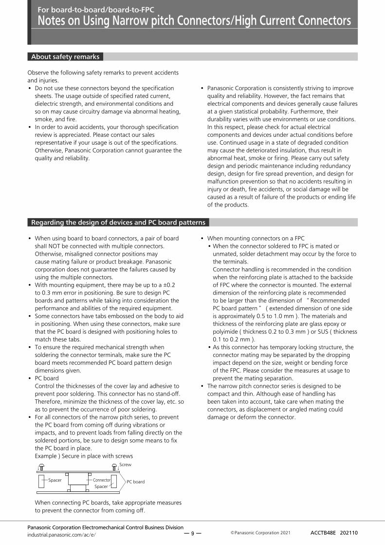
• For all connectors of the narrow pitch series, to prevent the PC board from coming off during vibrations or impacts, and to prevent loads from falling directly on the soldered portions, be sure to design some means to fix the PC board in place. Example ) Secure in place with screws
↓ ↓
ConnectorSpacer
Spacer PC board
Screw
When connecting PC boards, take appropriate measures to prevent the connector from coming off.
• When mounting connectors on a FPC• When the connector soldered to FPC is mated or
unmated, solder detachment may occur by the force to the terminals. Connector handling is recommended in the condition when the reinforcing plate is attached to the backside of FPC where the connector is mounted. The external dimension of the reinforcing plate is recommended to be larger than the dimension of “ Recommended PC board pattern ” ( extended dimension of one side is approximately 0.5 to 1.0 mm ). The materials and thickness of the reinforcing plate are glass epoxy or polyimide ( thickness 0.2 to 0.3 mm ) or SUS ( thickness 0.1 to 0.2 mm ).
• As this connector has temporary locking structure, the connector mating may be separated by the dropping impact depend on the size, weight or bending force of the FPC. Please consider the measures at usage to prevent the mating separation.
• The narrow pitch connector series is designed to be compact and thin. Although ease of handling has been taken into account, take care when mating the connectors, as displacement or angled mating could damage or deform the connector.
ー 9 ー

Notes on Using Narrow pitch Connectors/High Current Connectors
ACCTB48E 202110Panasonic Corporation 2021Panasonic Corporation Electromechanical Control Business Divisionindustrial.panasonic.com/ac/e/
Regarding soldering
■ Reflow soldering• Measure the recommended profile temperature for
reflow soldering by placing a sensor on the PC board near the connector surface or terminals. ( Please refer to the specification for detail because the temperature setting differs by products. )
• As for cream solder printing, screen printing is recommended.
• When setting the screen opening area and PC board foot pattern area, refer the recommended PC board pattern and window size of metal mask on the specification sheet, and make sure that the size of board pattern and metal mask at the base of the terminals are not increased.
• Please pay attentions not to provide too much solder. It makes miss mating because of interference at soldering portion when mating.
TerminalPaste solder
PC board foot pattern
• When mounting on both sides of the PC board and the connector is mounting on the underside, use adhesives or other means to ensure the connector is properly fixed to the PC board. ( Double reflow soldering on the same side is possible. )
• The condition of solder or flux rise and wettability varies depending on the type of solder and flux. Solder and flux characteristics should be taken into consideration and also set the reflow temperature and oxygen level.
• Do not use resin-containing solder. Otherwise, the contacts might be firmly fixed.
• Soldering conditions Please use the reflow temperature profile conditions recommended below for reflow soldering. Please contact our sales representative before using a temperature profile other than that described below ( e.g. lead-free solder )
60 to 120 sec.
Preheating
Time
Temperature Peak temperature
200℃220℃
260℃230℃180℃150℃
70 sec.
25 sec.Upper limited (Solder heat resistance)Lower limited (Solder wettability)
For products other than the ones above, please refer to the latest product specifications.
• The temperature profiles given in this catalog are values measured when using the connector on a resin-based PC board. When performed reflow soldering on a metal board ( iron, aluminum, etc. ) or a metal table to mount on a FPC, make sure there is no deformation or discoloration of the connector before mounting.
• Please contact our sales representative when using a screen-printing thickness other than that recommended.
Regarding the selection of the connector placement machine and the mounting procedures
• Select the placement machine taking into consideration the connector height, required positioning accuracy, and packaging conditions.
• Be aware that if the chucking force of the placement machine is too great, it may deform the shape of the connector body or connector terminals.
• Be aware that during mounting, external forces may be applied to the connector contact surfaces and terminals and cause deformations.
• Depending on the size of the connector being used, self alignment may not be possible. In such cases, be sure to carefully position the terminal with the PC board pattern.
• The positioning bosses give an approximate alignment for positioning on the PC board. For accurate positioning of the connector when mounting it to the PC board, we recommend using an automatic positioning machine.
• In case of dry condition, please note the occurrence of static electricity. The product may be adhered to the embossed carrier tape or the cover tape in dry condition. Recommended humidity is from 40 to 60% RH and please remove static electricity by ionizer in manufacturing process.
ー 10 ー
Notes on Using Narrow pitch Connectors/High Current Connectors
ACCTB48E 202110Panasonic Corporation 2021Panasonic Corporation Electromechanical Control Business Divisionindustrial.panasonic.com/ac/e/
■ Hand soldering• Set the soldering iron so that the tip temperature is less
than that given in the table below.Table A
Product name Soldering iron temperature
SMD type connectors all products 300℃ within 5 sec.350℃ within 3 sec.
• Do not allow flux to spread onto the connector leads or PC board. This may lead to flux rising up to the connector inside.
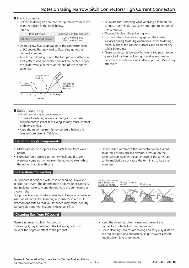
• Touch the soldering iron to the foot pattern. After the foot pattern and connector terminal are heated, apply the solder wire so it melts at the end of the connector terminals.
Apply the solder wire here
Terminal
Pattern
Small angle as possible up to 45 degrees
Soldering
iron
PC board
• Be aware that soldering while applying a load on the connector terminals may cause improper operation of the connector.
• Thoroughly clean the soldering iron.• Flux from the solder wire may get on the contact
surfaces during soldering operations. After soldering, carefully check the contact surfaces and clean off any solder before use.
• These connector is low profile type. If too much solder is supplied for hand soldering, It makes miss mating because of interference at soldering portion. Please pay attentions.
■ Solder reworking• Finish reworking in one operation.• In case of soldering rework of bridges. Do not use
supplementary solder flux. Doing so may cause contact problems by flux.
• Keep the soldering iron tip temperature below the temperature given in Table A.
Handling single components
• Make sure not to drop or allow parts to fall from work bench.
• Excessive force applied to the terminals could cause warping, come out, or weaken the adhesive strength of the solder. Handle with care.
• Do not insert or remove the connector when it is not soldered. Forcibly applied external pressure on the terminals can weaken the adherence of the terminals to the molded part or cause the terminals to lose their evenness.
Precautions for mating
Cleaning flux from PC board
This product is designed with ease of handling. However, in order to prevent the deformation or damage of contacts and molding, take care and do not mate the connectors as shown right.Our products are symmetrical structure. Please avoid reverse insertion of connector. Inserting a connector in a circuit direction opposite to that you intended may cause circuitry damage via abnormal heating, smoke, and fire.
Tilted matingStrongly pressed and twisted
Press-fitting while the mating inlets of the socket and header are not matched.
There is no need to clean this product. If cleaning it, pay attention to the following points to prevent the negative effect to the product.
• Keep the cleaning solvent clean and prevent the connector contacts from contamination.
• Some cleaning solvents are strong and they may dissolve the molded part and characters, so pure water passed liquid solvent is recommended.
ー 11 ー

Notes on Using Narrow pitch Connectors/High Current Connectors
ACCTB48E 202110Panasonic Corporation 2021Panasonic Corporation Electromechanical Control Business Divisionindustrial.panasonic.com/ac/e/
Please refer to "the latest product specifications"when designing your product.•Requests to customers:https://industrial.panasonic.com/ac/e/salespolicies/
Handling the PC board
Storage of connectors
Other Notes
■ Handling the PC board after mounting the connectorWhen cutting or bending the PC board after mounting the connector, be careful that the soldered sections are subjected to excessive force.
The soldered areas should not be subjected to force.
• To prevent problems from voids or air pockets due to heat of reflow soldering, avoid storing the connectors in areas of high humidity.
• Depending on the connector type, the color of the connector may vary from connector to connector depending on when it is produced. Some connectors may change color slightly if subjected to ultraviolet rays during storage. This is normal and will not affect the operation of the connector.
• When storing the connectors with the PC boards assembled and components already set, be careful not to stack them up so the connectors are subjected to excessive forces.
• Avoid storing the connectors in locations with excessive dust. The dust may accumulate and cause improper connections at the contact surfaces.
• Do not remove or insert the electrified connector ( in the state of carrying current or applying voltage ).
• Dropping of the products or rough mishandling may bend or damage the terminals and possibly hinder proper reflow soldering.
• Before soldering, try not to insert or remove the connector more than absolutely necessary.
• When coating the PC board after soldering the connector to prevent the deterioration of insulation, perform the coating in such a way so that the coating does not get on the connector.
• There may be variations in the colors of products from different production lots. This is normal.
• The connectors are not meant to be used for switching.• Product failures due to condensation are not covered by
warranty.
Regarding sample orders to confirm proper mounting
When ordering samples to confirm proper mounting with the placement machine, connectors are delivered in 50-piece units in the condition given right. Consult a sale representative for ordering sample units.
Condition when delivered from manufacturing
Required numberof products for
sample productionEmbossed tape amount required for the mounting ( Unit 50 pcs. )
ReelDelivery can also be made on a reel by customer request.
ー 12 ー

Please contact ..........
Electromechanical Control Business Division
industral.panasonic.com/ac/e/
Specifications are subject to change without notice.
1006, Oaza Kadoma, Kadoma-shi, Osaka 571-8506, Japan
©Panasonic Corporation 2021
ACCTB112E 202110