high efficiency single-crystal cdte solar cell€¦ · 2 | solar energy technologies program...
TRANSCRIPT

1 | Program Name or Ancillary Text eere.energy.gov
Solar Energy Technologies Program Peer Review
High Efficiency Single Crystal CdTe Solar Cells
Dr. Michael CarmodyEPIR Technologies [email protected], 2010Program Team: PV
The world leader in II-VI material technology and innovation

2 | Solar Energy Technologies Program eere.energy.gov
Objective
Long Term Goal:– Develop high efficiency multijunction, single crystal II-VI/Si solar cells.
Silicon Solar Cell
p-side Ohmic contact
In
Tunnel Junction
In
Single Crystal p-type CdZnTe (Eg ~ 1.75 eV)
n-type CdZnTe (Eg ~ 1.75)
Tandem Junction Triple Junction Cell
Top
cell
Bot
tom
cell
p++n++n+
p++n++
p++n++
p- contact
p+
p-type Silicon
p-type Cd1-xZnxTeTCO
p-side Contact
Single Junction Cell Architecture
Preincubator Program Goal:– Develop high efficiency single junction single crystal II-VI on Si solar cells.
3 | Solar Energy Technologies Program eere.energy.gov
3
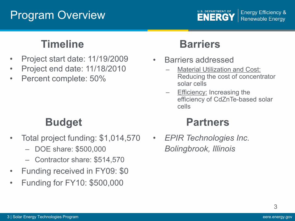
• Project start date: 11/19/2009• Project end date: 11/18/2010• Percent complete: 50%
• Barriers addressed– Material Utilization and Cost:
Reducing the cost of concentrator solar cells
– Efficiency: Increasing the efficiency of CdZnTe-based solar cells
• Total project funding: $1,014,570– DOE share: $500,000– Contractor share: $514,570
• Funding received in FY09: $0• Funding for FY10: $500,000
Timeline
Budget
Barriers
• EPIR Technologies Inc.Bolingbrook, Illinois
Partners
Program Overview

4 | Solar Energy Technologies Program eere.energy.gov
Why High Efficiency II-VI on Si?
1. High absorption coefficient.
2. Ideal single junction bandgap (~ 1.5 eV).
3. Bandgap tunable from 1.5 to 2.24 eV (Cd1-xZnxTe).
4. Higher accessible bandgaps than III-V’s because of lattice matching issues.
5. II-VI devices appear to be less impacted by defects such as dislocations.
- more ionic, less covalent nature of II-VI materials
- greater screening that lowers the cross-section and capture rates of traps
- impurity or defect states in more ionic materials should have substantially
fewer deep energy levels and hence should not give rise to nearly as rapid
carrier recombination (longer lifetimes)
6. Potential to grow on low cost large format substrates such as silicon.
- lattice mismatch less important

5 | Solar Energy Technologies Program eere.energy.gov
Why High Efficiency II-VI on Si?
Calculated Multijunction Cell Efficiencies (with C = 3 mA/cm2-K3)II-VI Multijunction Solar Cell Efficiencies III-V Multijunction Solar Cell Efficiencies
(III-V junction Eg ≤ 1.88 eV)Cell (with Si optical path
length and junction energies)
One-sunefficiency
(%)
500-sunsefficiency
(%)
Cell (with Ge optical path length and junction
energies)
One-sunefficiency
(%)
500-sunsefficiency
(%)
II-VI/Si (500 µm)
1.78/1.12 eV39.3 44.1 III-V/Ge (500 µm)
1.5-1.6/0.67 eV 33.6 40.2
II-VI/II-VI/Si (500 µm)
2.06/1.52/1.12 eV45.3 51.5 III-V/III-V/Ge (500 µm)
1.68/1.18/0.67 eV36.2 43.6
Inverted 3-junction
1.96/1.40/0.95 eV46.0 54.0 Inverted 3-junction
1.88/1.35/0.94 eV43.6 50.6
D. Xu et al., Appl. Phys. Lett. 96, 073508 (2010).
Multijunction II-VI/II-VI/Si cells have the theoretical potential to reach higher efficiencies than their III-V counterparts because of the wider range of accessible bandgaps than the III-Vs.

6 | Solar Energy Technologies Program eere.energy.gov
Potential Manufacturing Advantages of II-VI/Si vs. III-V/Ge Solar Cells
• Gas-based delivery system using arsine, phosgene, etc. => safety precautions, regulatory approval difficult => added expense, slow expansion of capacity
• High maintenance, much down time => added expense
• Small area, expensive Ge, GaAs or InP substrates => higher cost
• Doping and contacting are well solved problems
• MOCVD Growth of III-Vs • MBE Growth of II-VIs
• Delivery system based on molecular beams => easier safety precautions and regulatory approval
• Much lower maintenance requirements and downtime
• Larger area, much less expensive and more robust Si substrates can be used
• Slower growth rate, but high throughput, ~24,000 6 in. wafers for Riber 7000 MBE machine (10 MW/yr at 500 suns, 4 MW/yr at 200 suns)

7 | Solar Energy Technologies Program eere.energy.gov
The II-VI Voc Challenge
0
0.2
0.4
0.6
0.8
1
1.2
1.4
1.6
1.8
2
0.8 1.0 1.2 1.4 1.6 1.8 2.0 2.2
V oc(
V)
Eg(eV)
Thermodynamic Limit
GaAs
Si
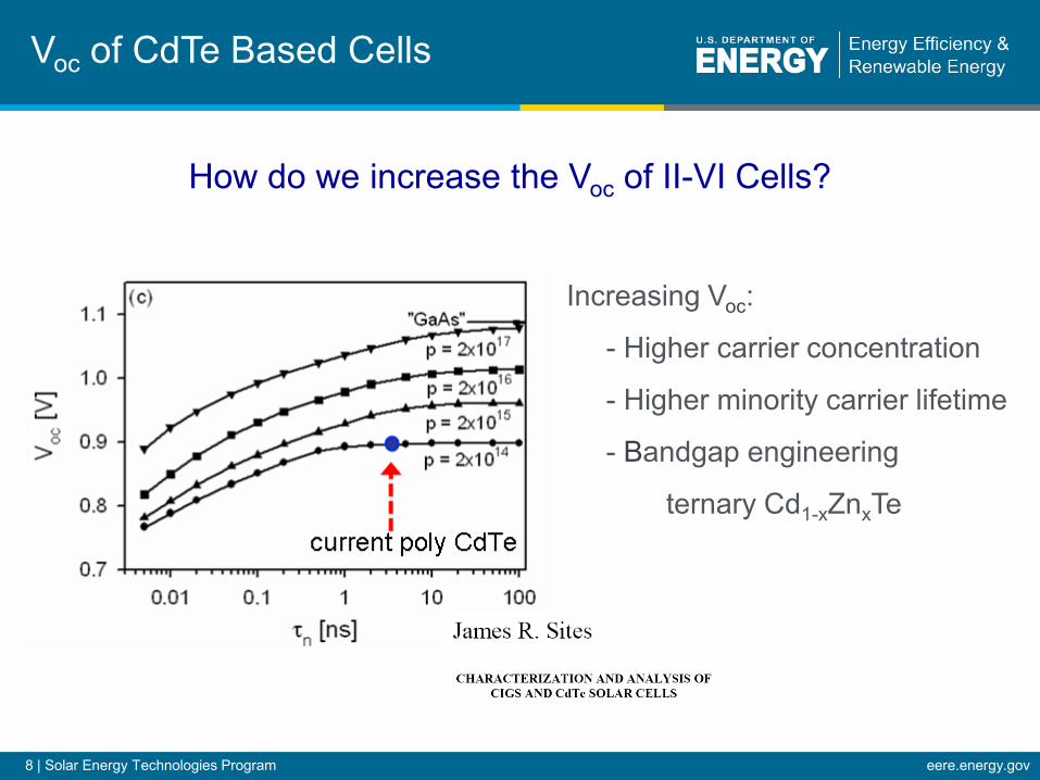
From R. R. King, Stanford Photonics Research Center Symposium, Stanford, CA, Sept. 14-16, 2009thin film poly-CdTe
Current thin film CdTe cells have suppressed Voc relative to Si and III-V based cells
η =JscVocFF
Pin
Single junction GaAs 1-sun efficiency record - 24.7% - 2008 IMEC
Single junction CdTe 1-sun efficiency record - 16.5% - 2001 NREL
Current CdTe Thin Film Cells
- low carrier concentration < 1015 cm-3 p-type- low minority carrier lifetime (< 10 ns)- Voc significantly lower than bandgap predicts
Eg – qVoc measures the intrinsic cell qualityJsc and FF depend on extrinsic factors
8 | Solar Energy Technologies Program eere.energy.gov
Voc of CdTe Based Cells
How do we increase the Voc of II-VI Cells?
Increasing Voc:
- Higher carrier concentration
- Higher minority carrier lifetime
- Bandgap engineering
ternary Cd1-xZnxTe
9 | Solar Energy Technologies Program eere.energy.gov
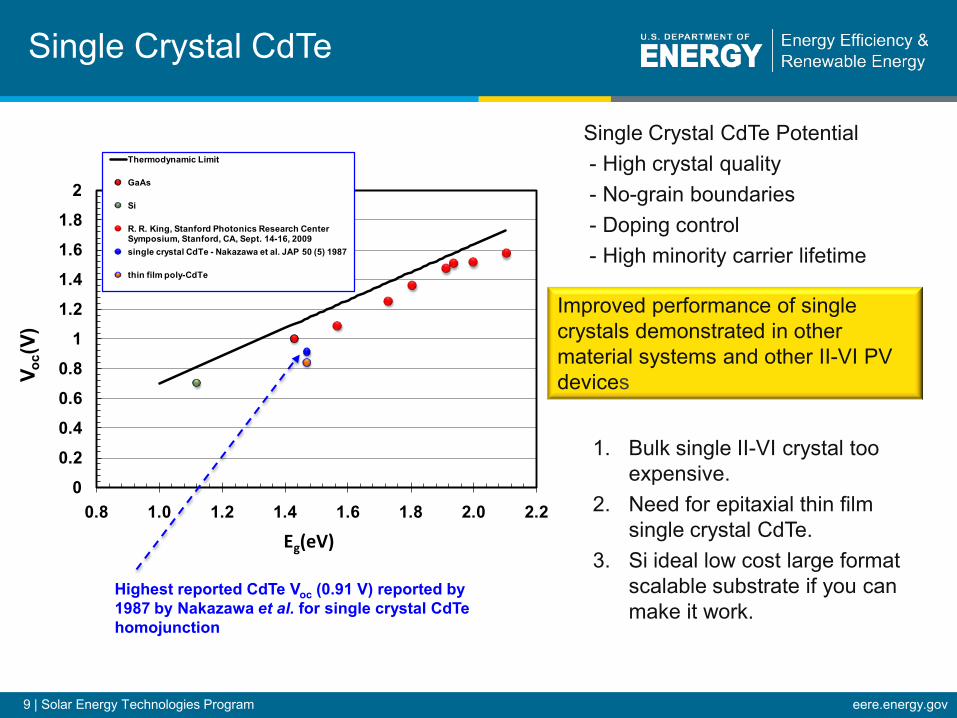
Single Crystal CdTe
0
0.2
0.4
0.6
0.8
1
1.2
1.4
1.6
1.8
2
0.8 1.0 1.2 1.4 1.6 1.8 2.0 2.2
V oc(
V)
Eg(eV)
Thermodynamic Limit
GaAs
Si
R. R. King, Stanford Photonics Research Center Symposium, Stanford, CA, Sept. 14-16, 2009single crystal CdTe - Nakazawa et al. JAP 50 (5) 1987
thin film poly-CdTe
Highest reported CdTe Voc (0.91 V) reported by 1987 by Nakazawa et al. for single crystal CdTe homojunction
Single Crystal CdTe Potential- High crystal quality- No-grain boundaries- Doping control- High minority carrier lifetime
1. Bulk single II-VI crystal too expensive.
2. Need for epitaxial thin film single crystal CdTe.
3. Si ideal low cost large format scalable substrate if you can make it work.
Improved performance of single crystals demonstrated in other material systems and other II-VI PV devices

10 | Solar Energy Technologies Program eere.energy.gov
Program Tasks
Task 1: MBE growth and characterization of single-crystal epitaxial CdTe/Si.
Task 2: Establish low resistance Ohmic contacts for n-type CdTe.
Task 3: Perform controlled n- and p-doping in plain CdTe and measure the dopant
densities and carrier concentrations.
Task 4: Measurement of the CdTe minority carrier recombination lifetimes.
Task 5: Model the photon absorption and electrical carrier transport in CdTe/Si solar
cells and their efficiencies.
Task 6: Fabricate CdTe p-n homojunctions and characterize them with I-V and C-V.
Task 7: Fabricate and test CdTe/Si homojunction solar cells.

11 | Solar Energy Technologies Program eere.energy.gov
Key Program Milestones
The internal decision milestones:
(1)Doping Development;
> 2×1015 cm-3 p-type
> 2×1016 cm-3 n-type
(2)Minority carrier recombination lifetime in p-doped material ≥ 50 ns
(3)The achievement of a diode ideality factor < 2
(4)The achievement of a solar cell with an efficiency >10%

12 | Solar Energy Technologies Program eere.energy.gov
Architecture Approach
p-type Silicon
p-type Cd1-xZnxTe
As-grown
p-type Silicon
p-type Cd1-xZnxTeTCO
p-side Contact
Single Junction Cell Architecture
n-on-p homojunction in the single crystal CdTe or CdZnTe cell

13 | Solar Energy Technologies Program eere.energy.gov
Deposition Technology - MBE
XRD DCRC FWHM Map – 3” CdTe on Si
CdTe/As/Si(111) interfaceCdTe/As/Si(111) interface
MBE Crystal Growth of II-VI on SiLow Temperature Growth
1. doping control in II-VI semiconductors
2. advanced structures- heterojunctions- bandgap grading- doping grading
0
50
100
150
200
250
300
350
400
0 20 40 60 80
DCR
C FW
HM
(ar
c se
c)
CdTe Layer Number
Single Crystal CdTe on Si at EPIR
DCRC FWHM (center)
D08105
Program Deliverable
Program Deliverable

14 | Solar Energy Technologies Program eere.energy.gov
Doping Control
Both p and n type doping control required for PV devices
Doping control traditionally a challenge in CdTe based cells.
1.E+13
1.E+14
1.E+15
1.E+16
11.11.21.31.41.51.61.71.8
C-V
C.C
. (cm
-3)
Depth from interface (um)
after annealno anneal
- Cd vacancy influence on doping in CdTe- Cd and Zn vacancy controls doping in CdZnTe
C-V Depth Profile of Vacancy Doped CdTe
“as-grown” CdTe layers slightly p-type
Post growth anneals- increase the Cd or Zn vacancy conc.

15 | Solar Energy Technologies Program eere.energy.gov
N-type Doping Control
0
200
400
600
800
1000
1200
1400
1600
mob
ility
(cm
2/Vs
) RTP
Closed tube
Hall Carrier Concentration Hall Mobility
*State of the art CdTe n-type mobility ~ 1500 cm2/Vs*SIMS dopant level ~ 1018 cm-2
n-type doped CdTe
1E+16
1E+17
1E+18
1E+19
carr
ier c
once
ntra
tion
(cm
-3)
program goal > 5e16 cm-3
16 | Solar Energy Technologies Program eere.energy.gov
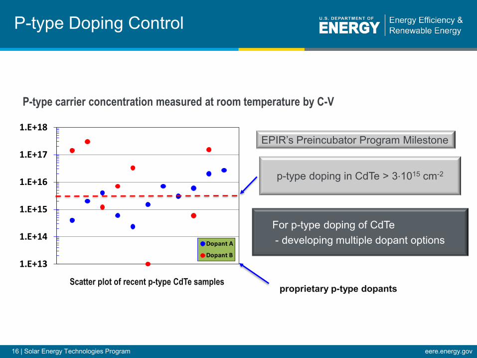
P-type Doping Control
Scatter plot of recent p-type CdTe samples
P-type carrier concentration measured at room temperature by C-V
1.E+13
1.E+14
1.E+15
1.E+16
1.E+17
1.E+18
Dopant A
Dopant B
p-type doping in CdTe > 3·1015 cm-2
For p-type doping of CdTe - developing multiple dopant options
proprietary p-type dopants
EPIR’s Preincubator Program Milestone
17 | Solar Energy Technologies Program eere.energy.gov
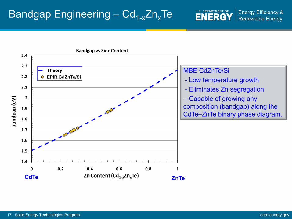
Bandgap Engineering – Cd1-xZnxTe
MBE CdZnTe/Si - Low temperature growth- Eliminates Zn segregation- Capable of growing any composition (bandgap) along the CdTe–ZnTe binary phase diagram.
CdTe ZnTe
1.4
1.5
1.6
1.7
1.8
1.9
2
2.1
2.2
2.3
2.4
0 0.2 0.4 0.6 0.8 1
band
gap
(eV
)
Zn Content (Cd1-xZnxTe)
Bandgap vs Zinc Content
TheoryEPIR CdZnTe/Si

18 | Solar Energy Technologies Program eere.energy.gov
Device Development Pathway
p-type Silicon
p-type Cd1-xZnxTeTCO
p-side Contact
Single Junction Cell Architecture
Measured under AM1.5
19 | Solar Energy Technologies Program eere.energy.gov
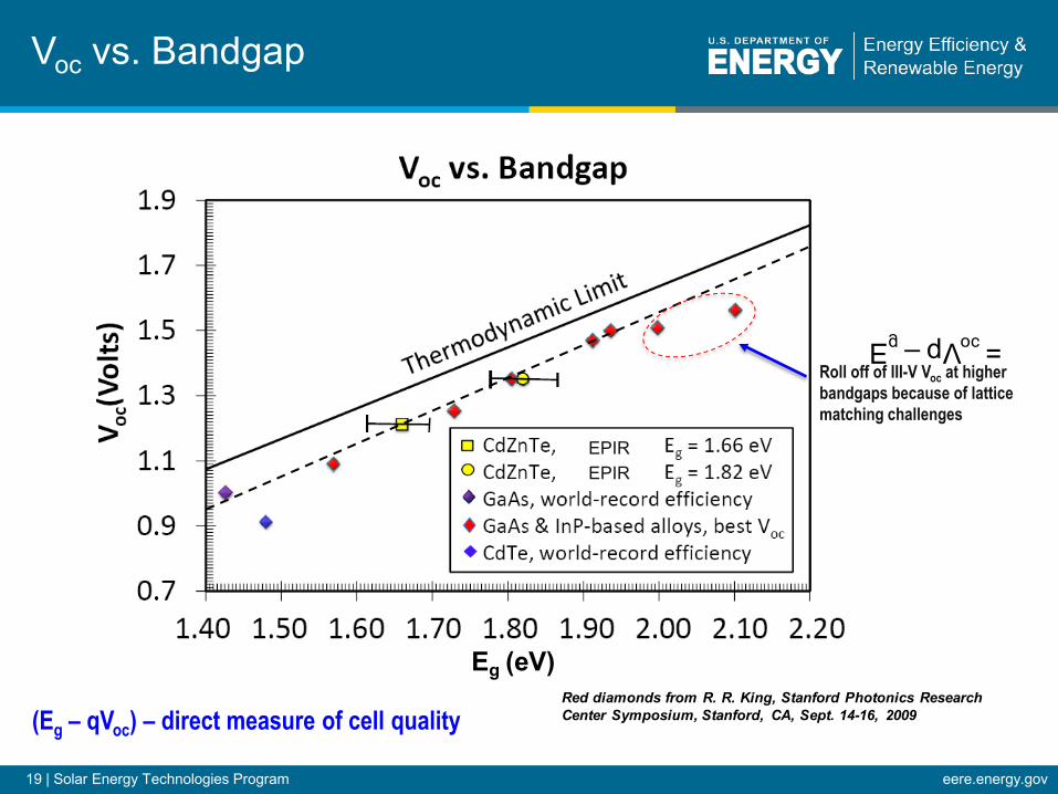
Voc vs. Bandgap
Eg (eV)Red diamonds from R. R. King, Stanford Photonics Research Center Symposium, Stanford, CA, Sept. 14-16, 2009
EPIREPIR
(Eg – qVoc) – direct measure of cell quality
Roll off of III-V Voc at higher bandgaps because of lattice matching challenges

20 | Solar Energy Technologies Program eere.energy.gov
Tandem Cell Development
Silicon Solar Cell
p-side Ohmic contact
In
Tunnel Junction
In
Single Crystal p-type CdZnTe (Eg ~ 1.75 eV)
n-type CdZnTe (Eg ~ 1.75)
Tandem Junction Triple Junction Cell
Top
cell
Bot
tom
cell
p++n++n+
p++n++
p++n++
p- contact
p+
Early Tandem Cell Development at EPIR
CdZnTe top cell (Eg ~ 1.8 eV) – Voc ~ 1.3 eVSi – bottom cell – Voc ~ 0.45 eV
Voltage addition demonstrated on early EPIR tandem cell device
Related Work

21 | Solar Energy Technologies Program eere.energy.gov
Future Plans
Deliverable 1. (Complete) An epitaxial CdTe film on a 3-inch Si wafer representing the baseline of the proposed
technology will be delivered during month one. The CdTe/Si wafer will be delivered with a high resolution XRD data mapping
across the entire wafer to show the uniformity of the structural quality.
Deliverable 2. (Complete) A single-crystal, extrinsically doped n-type CdTe/Si piece cut from a 3” wafer with data obtained
from adjacently cut pieces showing an n-type carrier concentration within the range 3×1016 cm-3 to 3×1018 cm-3.
Remaining 2010 Deliverables
Deliverable 3. on track (due June 18th) A single-crystal, extrinsically doped p-type CdTe/Si piece cut from a 3” wafer
with data obtained from adjacently cut pieces showing a p-type carrier concentration within the range 3×1015 cm-3 to 3×10¹⁷
cm-3.
Deliverable 4. A single-crystal, extrinsically doped p-type CdTe/Si piece cut from a 3” wafer with data obtained from
adjacently cut pieces showing a minority carrier lifetime longer than 100ns.
Deliverable 5. A prototype CdTe solar cell with a 15% efficiency will be delivered during month 12 – November 2010
22 | Solar Energy Technologies Program eere.energy.gov
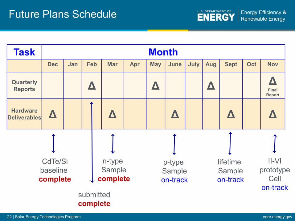
Future Plans Schedule
Task MonthDec Jan Feb Mar Apr May June July Aug Sept Oct Nov
Quarterly Reports Δ Δ Δ Δ
Final Report
HardwareDeliverables Δ Δ Δ Δ Δ
CdTe/Sibaseline complete
n-type Sample
complete
p-type Sampleon-track
lifetime Sampleon-track
II-VI prototype
Cellon-track
submittedcomplete
23 | Solar Energy Technologies Program eere.energy.gov
Budget
• Total project funding: $1,014,570• DOE share: $500,000• Contractor share: $514,570
• Funding received in FY09: $0• Funding for FY10: $500,000• Project is on time and on budget.• Tasks to be added if additional funding were made available:
• Multijunction cell development a. CdZnTe growth and optimizationb. Tunnel junction optimization - Si/Si, Si/CZT and CZT/CZT
• Project ends in 2010. Thus no changes for 2011 exist.

24 | Solar Energy Technologies Program eere.energy.gov
24
• Single crystal CdTe and CdTe based alloys have the potential to dramatically increase the efficiency of single junction CdTe based solar cells with efficiencies comparable to single crystal GaAs cells.
• Single crystal CdTe and CdTe based alloys grown on Si have the potential to act as a platform for low cost high performance multijunction solar cells with theoretical efficiencies greater than comparable III-V cells.
• The Preincubator program is on track with all program deliverables met to date and the remaining program deliverables are on track to be delivered on time and on budget.
• Preliminary cell results serve as a proof of concept that the single crystal II-VI on Si approach is a viable technology pathway for future high efficiency cell development.
Summary

25 | Solar Energy Technologies Program eere.energy.gov
Summary
Program Performance Metric
Parameter or Deliverable
Status in FY09 Result in FY10 Notes
FHWM < 200 arcsec
Rocking curve FWHM CdTe/Si
Completed NA Sample delivered to NREL for verification
> 3e16 cm-3 N-type carrier concentration
Completed NA Sample delivered to NREL for verification
> 3e15 cm-3 P-type carrier concentration
In progress In progress Demonstrated Internally –samples to be sent to NREL for verification June 2010
> 50 ns Minority carrier lifetime
In progress In progress Working with NREL to test
> 15% Single junction cell efficiency
In progress In progress Demonstrated preliminary devices