high electron mobility transistors (hemts) · schematic band diagram 2 deg ... ambacher et al, jap...
TRANSCRIPT

High Electron Mobility Transistors (HEMTs)
Active Region
Source DrainGate
S. I. Buffer
Lg
Wg
Active Region
Source DrainGate
S. I. Buffer
Lg
Wg
0 2 4 6 8 10 12 14 16
0
200
400
600
800
1000
gm = 200 mS/mm
∆∆∆∆VG = 1 V
VG = 2 V
I D (
mA
/mm
)
VDS
(V)
Open channel
Pinch off
Similar to normally-on MOSFETs but no substrate doping. For accurate formula, refer to Sze: Physics of Semiconductor Devices
d
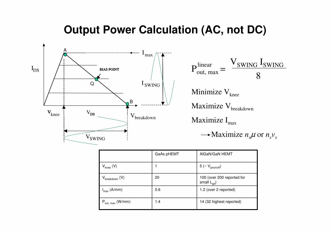
Output Power Calculation (AC, not DC)
Minimize Vknee
Maximize Vbreakdown
Maximize Imax
Maximize nsµ or nsvs
14 (32 highest reported)1.4 Pout, max (W/mm)
1.2 (over 2 reported)0.6Imax (A/mm)
100 (over 200 reported for
small Lgd)
20Vbreakdown (V)
5 (~ Vpinchoff)1Vknee (V)
AlGaN/GaN HEMTGaAs pHEMT
Vbreakdown
Imax
IDS
VDSV
knee
BIAS POINT
A
B
Q
VSWING
I SWING
DSV
BIAS POINT
DSV
BIAS POINT
V
BIAS POINT Pout, max =8
VSWING ISWINGlinear

Slide # 3
Sample power calculations• Let Vknee be 4 V, and Vbd be 120 V, and Iswing be 120 mA for a 100
micron gate width device. Calculate the maximum output power in
dBm and in W/mm
– Solution: Total maximum output power = 1/8 (120 – 4) 120 mW
= 1740 mW. So output power in dBm = 10 log1740 = 32.405
dBm. Output power density is 1740 mW/100 micron = 17400
mW/mm = 17.4 W/mm.
• If the gain is 15 dB, what is the input power?
– Solution: 10 log (Pout/Pin) = 15 ⇒ Pout = Pin x 101.5 = Pin x 31.62
⇒Pin = 17.4/31.62 = 0.5502 W/mm.
• If the dc input power is also given then the Power-Added
Efficiency (PAE) can be calculated as (Pout – Pin)/Pdc
Slide # 4
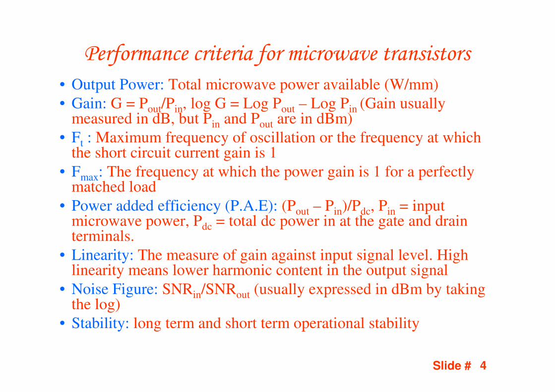
Performance criteria for microwave transistors
• Output Power: Total microwave power available (W/mm)
• Gain: G = Pout/Pin, log G = Log Pout – Log Pin (Gain usually measured in dB, but Pin and Pout are in dBm)
• Ft : Maximum frequency of oscillation or the frequency at which the short circuit current gain is 1
• Fmax: The frequency at which the power gain is 1 for a perfectly matched load
• Power added efficiency (P.A.E): (Pout – Pin)/Pdc, Pin = input microwave power, Pdc = total dc power in at the gate and drain terminals.
• Linearity: The measure of gain against input signal level. High linearity means lower harmonic content in the output signal
• Noise Figure: SNRin/SNRout (usually expressed in dBm by taking the log)
• Stability: long term and short term operational stability

Slide # 5
AlGaN/GaN HEMT: wish list
• High VBr
– Minimize
• Buffer leakage: GaN:Fe
• Gate leakage: Insulated-gate
– Other device structures to improve VBr
• High power efficiency
When efficiency is low
Power dissipation at semiconductor devices ↑
Ron ↑ efficiency ↓
• How to maximize efficiency
– Eliminate surface traps (passivation/epitaxial solutions)
– Eliminate bulk traps (growth condition tuning)
– Decrease leakage (low dislocation density/insulators?)

Slide # 6
Tiny changes in growth conditionshave strong effect on GaN properties(T,d, V/III)
+ very sensitive coalescence process
= process much less robust than homo-epitaxy
Lattice mismatch
High dislocation density in epitaxiallayers and at the interface of the heteroepitaxial layers.
Growth Challenge I: heteroepitaxy
time
Slide # 7
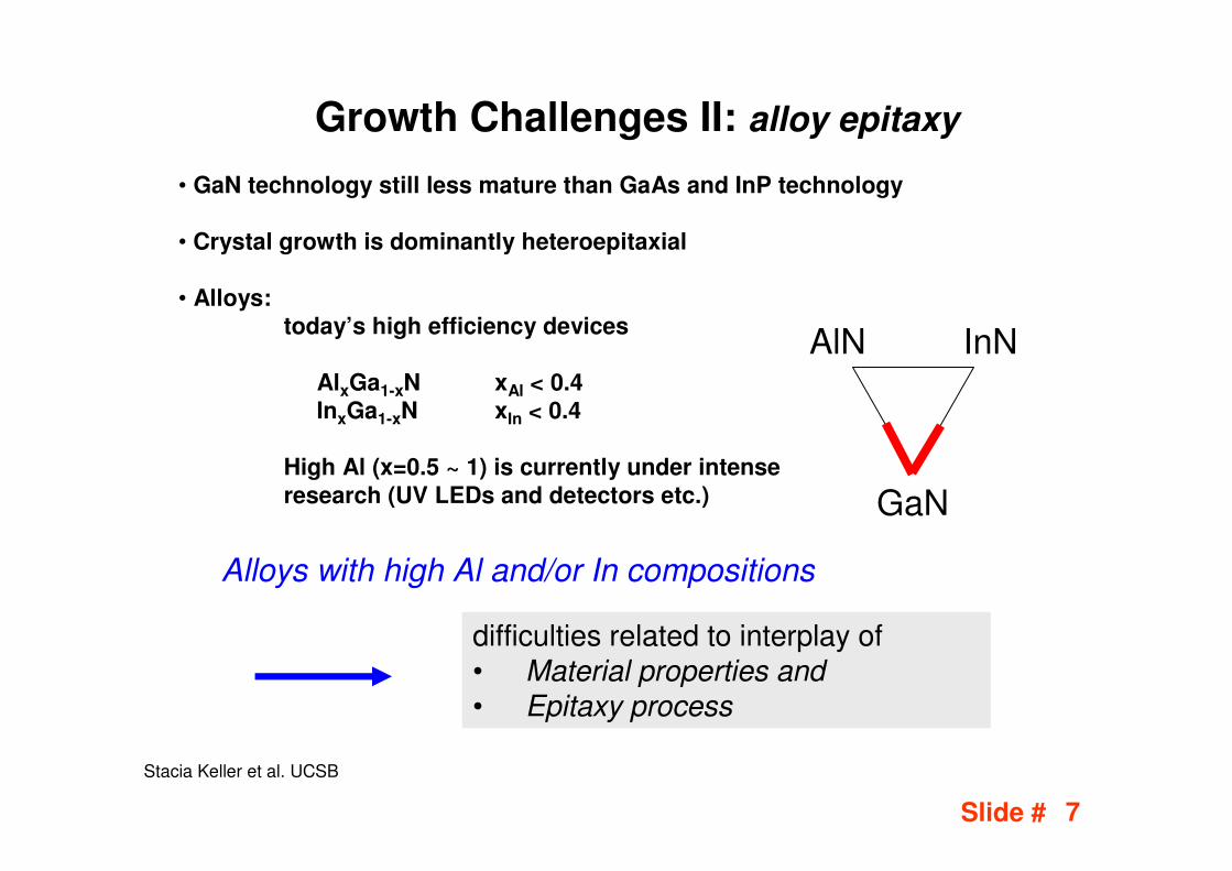
• GaN technology still less mature than GaAs and InP technology
• Crystal growth is dominantly heteroepitaxial
• Alloys:today’s high efficiency devices
AlxGa1-xN xAl < 0.4InxGa1-xN xIn < 0.4
High Al (x=0.5 ~ 1) is currently under intense
research (UV LEDs and detectors etc.) GaN
InNAlN
difficulties related to interplay of • Material properties and• Epitaxy process
Alloys with high Al and/or In compositions
Growth Challenges II: alloy epitaxy
Stacia Keller et al. UCSB
Slide # 8
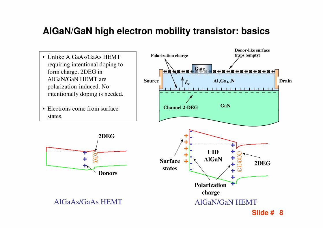
AlGaN/GaN high electron mobility transistor: basics
AlGaAs/GaAs HEMT AlGaN/GaN HEMT
• Unlike AlGaAs/GaAs HEMT
requiring intentional doping to
form charge, 2DEG in
AlGaN/GaN HEMT are
polarization-induced. No
intentionally doping is needed.
• Electrons come from surface
states.
2DEG
Donors
---+++
2DEG
Polarization
charge
UID
AlGaNSurface
states
-------
+++++++
-----
+++++
⊕⊕⊕⊕ ⊕⊕⊕⊕ ⊕⊕⊕⊕ ⊕⊕⊕⊕ ⊕⊕⊕⊕ ⊕⊕⊕⊕ ⊕⊕⊕⊕ ⊕⊕⊕⊕ ⊕⊕⊕⊕ ⊕⊕⊕⊕ ⊕⊕⊕⊕ ⊕⊕⊕⊕ ⊕⊕⊕⊕ ⊕⊕⊕⊕ ⊕⊕⊕⊕ ⊕⊕⊕⊕ ⊕⊕⊕⊕ ⊕⊕⊕⊕ ⊕⊕⊕⊕ ⊕⊕⊕⊕ ⊕⊕⊕⊕ ⊕⊕⊕⊕ ⊕⊕⊕⊕ ⊕⊕⊕⊕ ⊕⊕⊕⊕ ⊕⊕⊕⊕
Polarization charge
Donor-like surface
traps (empty)
AlxGa1-xN
GaN Channel 2-DEG
Gate
+ + + + + + + + + + + + + + + + + + + + + + + + ĒP
Drain Source
_ _ _ _ _ _ _ _ _ _ _ _ _ _ _ _ _ _ _ _
_ _ _ _ _ _ _ _ _ _ _ _ _ _ _ _ _ _ _ _ _
Slide # 9
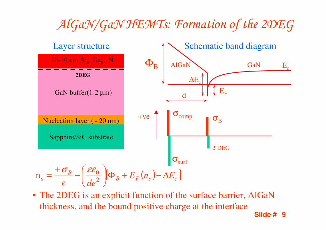
AlGaN/GaN HEMTs: Formation of the 2DEG
• The 2DEG is an explicit function of the surface barrier, AlGaN
thickness, and the bound positive charge at the interface
20-30 nm Al0.3Ga0.7 N
GaN buffer(1-2 µm)
Nucleation layer (~ 20 nm)
Sapphire/SiC substrate
2DEG
Layer structure
ΦB
EF
∆Ec
AlGaN GaN
d
Ec
Schematic band diagram
2 DEG
σsurf
σBσcomp+ve
( )[ ]csFBB EnE
dee∆−+Φ
−
+=
2
0sn
εεσ

Slide # 10
Comparison with GaAs HEMT Physics
• No doping is required for the 2DEG to be present at the interface.
• Higher sheet charge and higher conduction band discontinuity forAlGaN/GaN heterostructure
AlGaAs
donor
layerGaAs buffer
AlGaAs spacer
AlGaAs/GaAs HEMT
ΦB
EF
∆Ec
AlGaN GaN
d
Ec
Schematic band diagram
2 DEG
σsurf
σBσcomp
+ve
Slide # 11
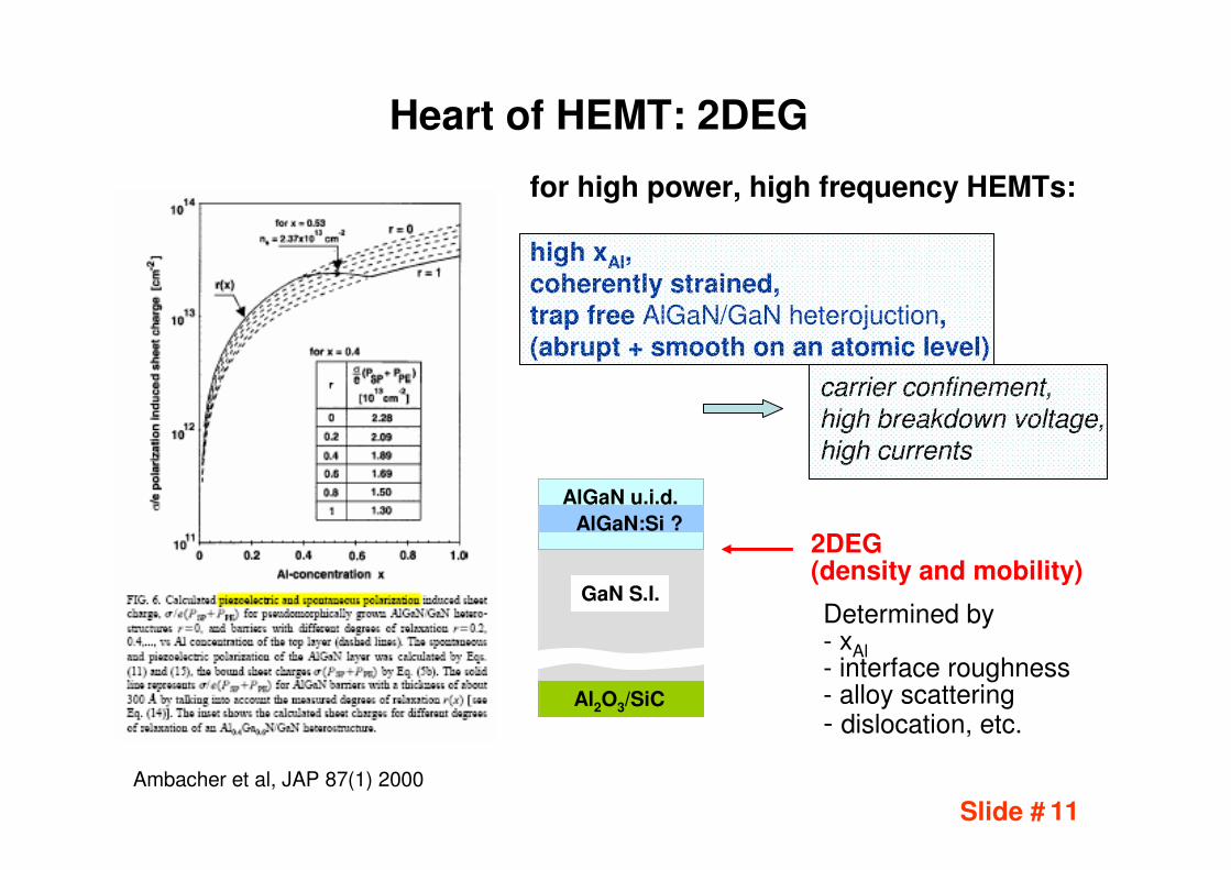
Heart of HEMT: 2DEG
2DEG (density and mobility)
for high power, high frequency HEMTs:
high xAl, coherently strained, trap free AlGaN/GaN heterojuction, (abrupt + smooth on an atomic level)
Al2O3/SiC
AlGaN u.i.d.
AlGaN:Si ?
GaN S.I.Determined by- xAl- interface roughness- alloy scattering- dislocation, etc.
carrier confinement,
high breakdown voltage,
high currents
Ambacher et al, JAP 87(1) 2000

Slide # 12
Properties of the 2DEG
• For AlGaAs/GaAs heterostructures, the spacer layer thickness is important for 2DEG mobility and density
• The 2DEG does not freeze out at very low temperature unlike the 3D doping
• The 2DEG mobility does not decrease with decrease in temperature unlike the 3D case
• The 2DEG mobility can increase with increase in 2DEG density due to increased screening unlike the 3D doping
Spacer layer
thickness vs.
2DEG density
and mobility
2DEG Mobility vs. density
dspacer depends on
intended application
Slide # 13
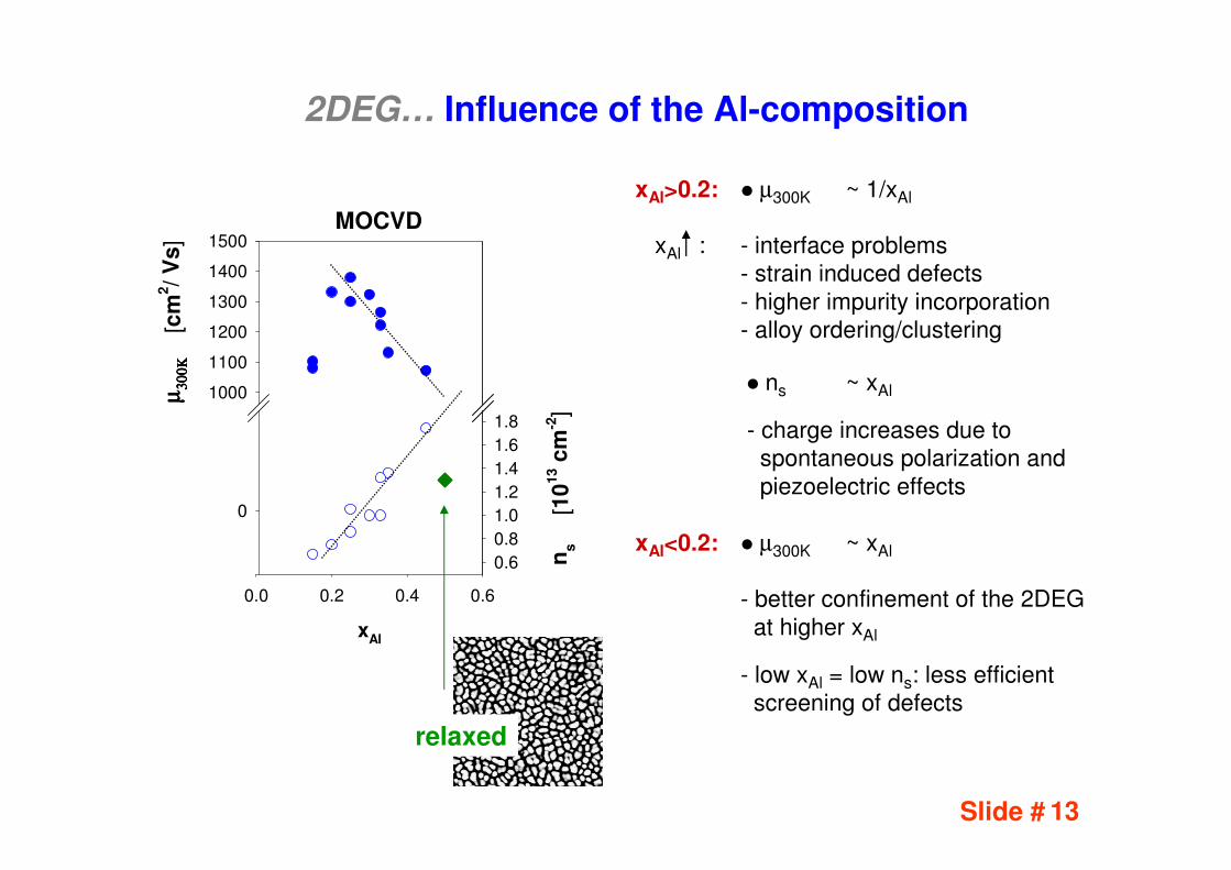
2DEG… Influence of the Al-composition
xAl>0.2: µ300K ~ 1/xAl
xAl : - interface problems
- strain induced defects
- higher impurity incorporation
- alloy ordering/clustering
ns ~ xAl
- charge increases due to
spontaneous polarization and
piezoelectric effects
xAl<0.2: µ300K ~ xAl
- better confinement of the 2DEG
at higher xAl
- low xAl = low ns: less efficient
screening of defects
xAl
0.0 0.2 0.4 0.6
ns
[1
013 c
m-2]
0.6
0.8
1.0
1.2
1.4
1.6
1.8
µµ µµ3
00
30
03
00
30
0ΚΚ ΚΚ [c
m2/ V
s]
0
1000
1100
1200
1300
1400
1500
relaxed
MOCVD
Slide # 14
Temperature dependence of v-F curve
• Usually the regions are separated into regions of constant and zero mobility
• A velocity overshoot is expected for GaN similar to GaAs case, but usually not seen, possibly due to high background doping
• At higher temperature, the degradation of v-F curve for GaN is much smaller than GaAs
0
1
2
3
0 200 400 600
Electric Field (kV/cm)
Ele
ctro
n V
eloci
ty (
10
7 c
m/s
)
300 K
500 K
700 K
0
1
2
3
0 4 8 12 16 20
Electric Field (kV/cm)
Ele
ctro
n V
eloci
ty (
10
7 c
m/s
)
300 K
500 K
700 K
GaN GaAs
Slide # 15
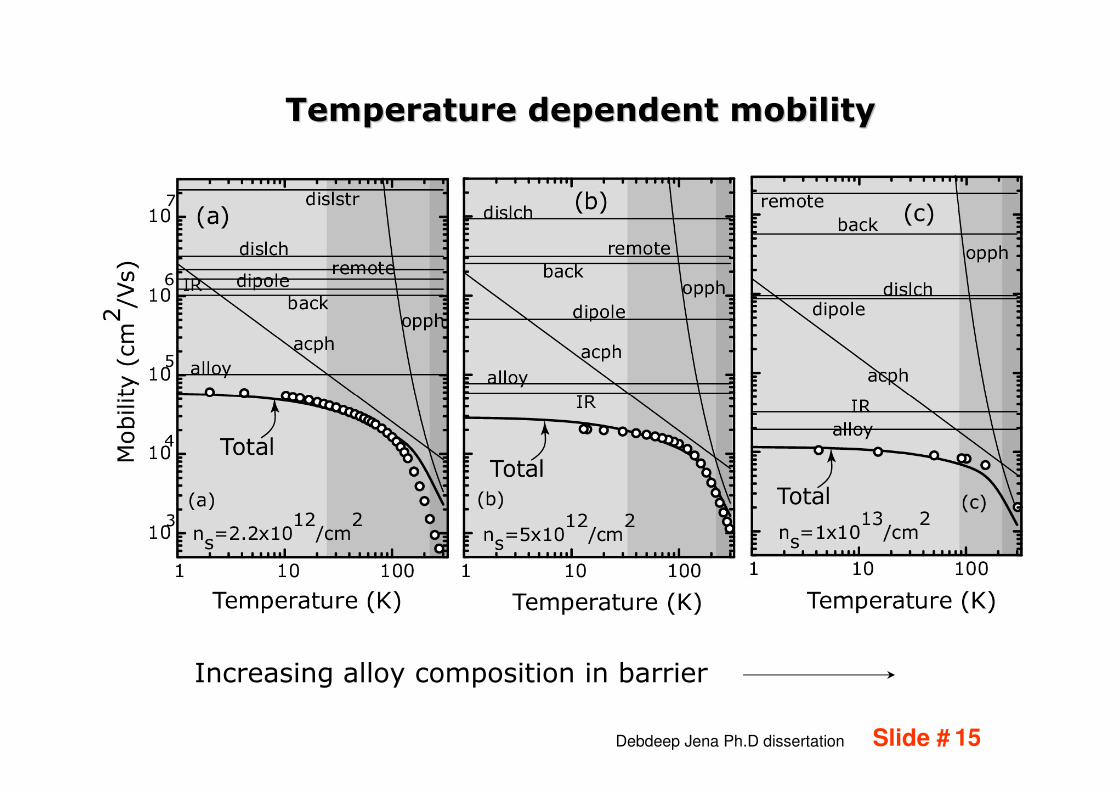
Temperature dependent mobilityTemperature dependent mobility
Increasing alloy composition in barrier
Debdeep Jena Ph.D dissertation
Slide # 16
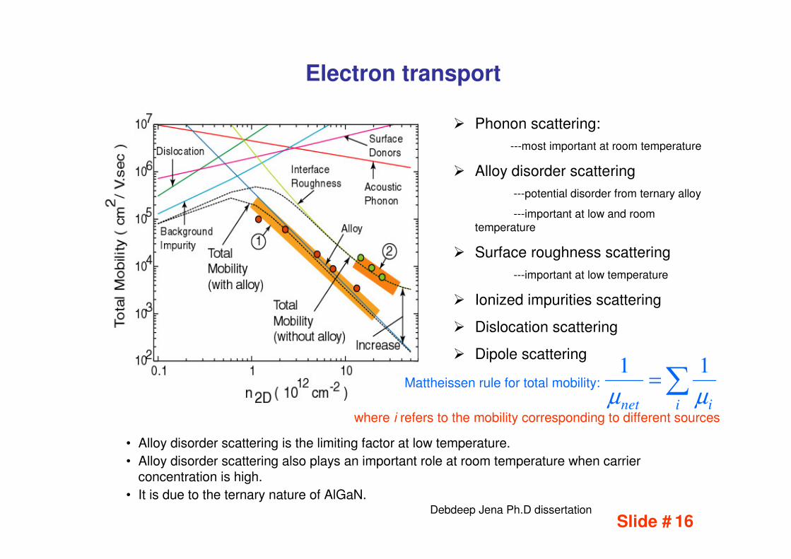
• Alloy disorder scattering is the limiting factor at low temperature.
• Alloy disorder scattering also plays an important role at room temperature when carrier concentration is high.
• It is due to the ternary nature of AlGaN.
Electron transport
Phonon scattering:
---most important at room temperature
Alloy disorder scattering
---potential disorder from ternary alloy
---important at low and room
temperature
Surface roughness scattering
---important at low temperature
Ionized impurities scattering
Dislocation scattering
Dipole scattering
Debdeep Jena Ph.D dissertation
Mattheissen rule for total mobility: ∑=i inet µµ
11
where i refers to the mobility corresponding to different sources
Slide # 17
Methods for reducing scattering• Controllable scattering mechanisms
– Background impurity scattering: By growing the
material purer
– Alloy scattering: By putting a thin binary alloy
(AlN) at the interface
– Dislocation scattering: By growing on lattice and
thermally matched substrate
– Interface roughness scattering: By growing very
smooth interfacial layers
• Rest of the scattering processes are usually
physics limited
Slide # 18
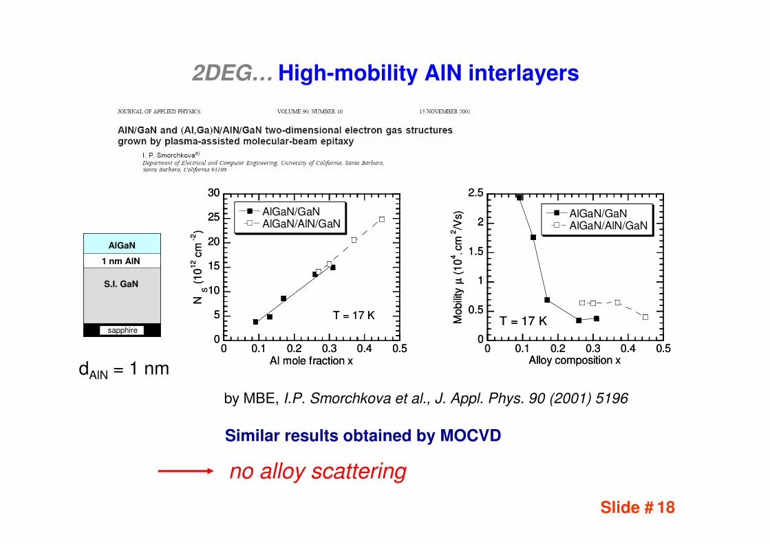
2DEG… High-mobility AlN interlayers
0
5
10
15
20
25
30
0 0.1 0.2 0.3 0.4 0.5
AlGaN/GaNAlGaN/AlN/GaN
N S (
10
12 c
m -
2)
Al mole fraction x
T = 17 K
0
0.5
1
1.5
2
2.5
0 0.1 0.2 0.3 0.4 0.5
AlGaN/GaNAlGaN/AlN/GaN
Mobili
ty µ
(10
4, cm
2/V
s)
Alloy composition x
T = 17 K
0
5
10
15
20
25
30
0 0.1 0.2 0.3 0.4 0.5
AlGaN/GaNAlGaN/AlN/GaN
N S (
10
12 c
m -
2)
Al mole fraction x
T = 17 K
0
0.5
1
1.5
2
2.5
0 0.1 0.2 0.3 0.4 0.5
AlGaN/GaNAlGaN/AlN/GaN
Mobili
ty µ
(10
4, cm
2/V
s)
Alloy composition x
T = 17 K
dAlN = 1 nm
Similar results obtained by MOCVD
1 nm AlN
S.I. GaN
sapphire
AlGaN
1 nm AlN
S.I. GaN
sapphire
AlGaN
by MBE, I.P. Smorchkova et al., J. Appl. Phys. 90 (2001) 5196
no alloy scattering

Slide # 19
AlN as a barrier layer
24 26 28 30 32 34 36
0.00
0.02
0.04
0.06
0.08 Al
0.22Ga
0.78N/GaN
AlN/GaN
AlGaN/GaN
interface
Pro
bab
ilit
y
Distance (nm)
• Use AlN as barrier material---No alloy disorder scattering:
higher mobility
---Higher polarization charge density:higher carrier concentration
• However, after gate metal deposition, it was found to be almost ohmic due to tunneling!
• Alloy disorder scattering:---Wavefunction penetration
---Ternary material: AlGaN
• Reduce alloy scattering:---Increase Al composition
---Binary material: AlN
0 5 10 15 20 25 300
1
2
3
4
5
6
2D
EG
den
sit
y (
10
13c
m-2)
AlN barrier thickness (nm)
Simulations

Slide # 20
25 nm Al0.3GaN
0.7-1 nm AlN
UID GaN
SiC Substrate
AlGaN/AlN/GaN Heterostructure
• Incorporation of a thin AlN (<1nm)
into a standard AlGaN/GaN HEMT
• The thickness of AlN interfacial
layer is below critical thickness for
formation of 2DEG. The main
purpose is to improve mobility.
• Thin AlN layer forms a larger
effective ∆Ec, which affects both
mobility and carrier concentration.
Slide # 21
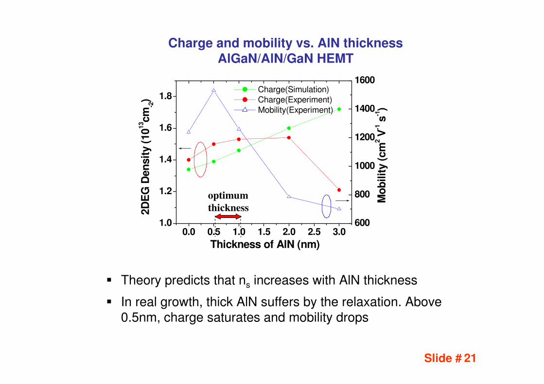
Charge and mobility vs. AlN thicknessAlGaN/AlN/GaN HEMT
Theory predicts that ns increases with AlN thickness
In real growth, thick AlN suffers by the relaxation. Above 0.5nm, charge saturates and mobility drops
0.0 0.5 1.0 1.5 2.0 2.5 3.01.0
1.2
1.4
1.6
1.8
Thickness of AlN (nm)
2D
EG
Den
sit
y (
10
13cm
-2)
Charge(Simulation)
Charge(Experiment)
Mobility(Experiment)
600
800
1000
1200
1400
1600
Mo
bilit
y (
cm
2 V
-1 s
-1)
optimum
thickness

Slide # 22
0 10 20 30 40 50-1
0
1
2
3
Thickness (nm)
En
erg
y (
eV
)
Thin AlN
----
++++
Effective ∆∆∆∆EC
0 10 20 30 40 50-1
0
1
2
3
Thickness (nm)
En
erg
y (
eV
)
Thin AlN
----
++++
Effective ∆∆∆∆EC
0 10 20 30 40 50
0
1
2
3
Thickness (nm)
En
erg
y (
eV
)
∆∆∆∆EC
AlGaN GaN
0 10 20 30 40 50
0
1
2
3
Thickness (nm)
En
erg
y (
eV
)
∆∆∆∆EC
AlGaN GaN
'0 0,2
0
AlGaN AlGaN B c eff
s
AlGaN AlN
t Eq q
nt t d
εε εεσ φ− + ∆
=+ +
0 0,2
0
AlGaN AlGaN B C AlGaN
s
AlGaN
t Eq q
nt d
εε εεσ φ⋅ − + ∆
=+
2'
, ,
0
c eff C AlGaN AlN AlN
qE E tσ
εε∆ = ∆ +
Band Diagram
25 nm Al0.33Ga0.67N/ 1 nm AlN/GaN HEMT 25 nm Al0.33Ga0.67N/GaN HEMT
Slide # 23
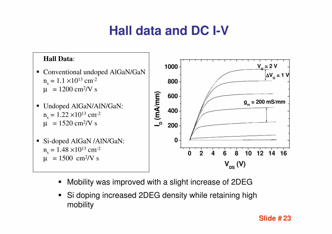
Hall Data:
Conventional undoped AlGaN/GaN
ns = 1.1 ×1013 cm-2
µ = 1200 cm2/V s
Undoped AlGaN/AlN/GaN:
ns = 1.22 ×1013 cm-2
µ = 1520 cm2/V s
Si-doped AlGaN /AlN/GaN:
ns = 1.48 ×1013 cm-2
µ = 1500 cm2/V s0 2 4 6 8 10 12 14 16
0
200
400
600
800
1000
gm = 200 mS/mm
∆∆∆∆VG = 1 V
VG = 2 V
I D (
mA
/mm
)V
DS (V)
Hall data and DC I-V
Mobility was improved with a slight increase of 2DEG
Si doping increased 2DEG density while retaining high mobility

Slide # 24
0 5 10 15 20 25 300
5
10
15
20
25
30
35
8.1 W/mm
PA
E (
%)
Pout
Gain
PAE
Po
ut
(dB
m),
Gain
(d
B)
Pin (dBm)
0
5
10
15
20
25
30
35
40
Power Performance
0 5 10 15 20 25 300
5
10
15
20
25
30
35
8.47 W/mm
PA
E (
%)
Pout
Gain
PAE
Po
ut
(dB
m),
Gain
(d
B)
Pin (dBm)
0
5
10
15
20
25
30
35
40
Undoped AlGaN Si-doped AlGaN
• On SiC substrate. SiN passivated.
• 8.1W/mm with a peak PAE of 23% was obtained at 8GHz at VD=50V,
ID=130mA/mm from an undoped AlGaN barrier HEMT.
• 8.47W/mm with a PAE of 41% was obtained at 10GHz at 8GHz at VD=45V,
ID=160mA/mm from a Si-doped barrier HEMT.

Slide # 25
0 50 100 150 200 250 300 350
Thickness (nm)
0
2
4
6
8
Ele
ctr
on
, H
ole
Co
ncen
trati
on
(10
18cm
-3)
Effect of Si doping density
0 50 100 150 200 250 300 350
-4
-2
0
2
4
Thickness (nm)
En
erg
y (
eV
)
0 50 100 150 200 250 300 350
Thickness (nm)
Nd/Polarization=1.2 Nd/Polarization=0.8 Nd/Polarization=0.5
ns = 1.7 ×××× 1013 cm-2
npara = 0.3 ×××× 1013 cm-2
ns = 1.36 ×××× 1013 cm-2 ns = 1.04 ×××× 1013 cm-2
ps = 0.18 ×××× 1013 cm-2
• Too much Si doping results in free electrons in graded layer, leading to parallel conduction
• Too little Si doping is not enough to remove holes• ~80% compensation puts fermi level in the middle of bandgap
holes
parallel conduction

Slide # 26
Design rules for AlGaN/GaN HEMTs:
Materials perspective• Thickness of the barrier layer: affects 2DEG
concentration and vertical gate field (which controls gate leakage current, VD, breakdown, and can also affect device degradation)
• Al composition of the barrier layer: affects 2DEG concentration and ∆EC, which confines the 2DEG
• Nucleation and buffer layer: affects dislocation density, and surface morphology (both affect mobility, one by charged line scattering and other by interface roughness scattering) and parasitic conduction.
• Substrate for epitaxial growth: affects the heat conductivity and ultimate output power performance as well as defect density, and parasitics.

Slide # 27
Transistor fabrication layout
Submicron Ni/Au
mushroom gate
defined by e-beamCl2 based ECR
mesa isolation
Air-bridge to connect
isolated source pads
1
2
34
Ti/Al/Ti/Au ohmic
contact annealed at
800˚C (0.3 to 0.6 Ω-mm)SEM photo showing air-bridge
over the gate metal (T-layout)SEM image of a submicron mushroom gate

Slide # 28
Design rules for AlGaN/GaN HEMTs:
Fabrication perspective
• The gate footprint and the cross-sectional area and width controls the frequency response
– Lg lower means fT goes up
– Cross-section and gate width control gate resistance (this is why mushroom gates are used)
• The gate drain spacing as well as gate footprint determines the breakdown voltage– Lg lower means VBR down
– Gate-drain spacing up means VBR up
• The geometry of the device also plays a role– The U-geometry device has 10 – 15 % lower gm, Idss due to self heating
2 x 125 µm U-gate
G
S
D
S
2 x 75 µm T-gate
S S
D
G
Slide # 29
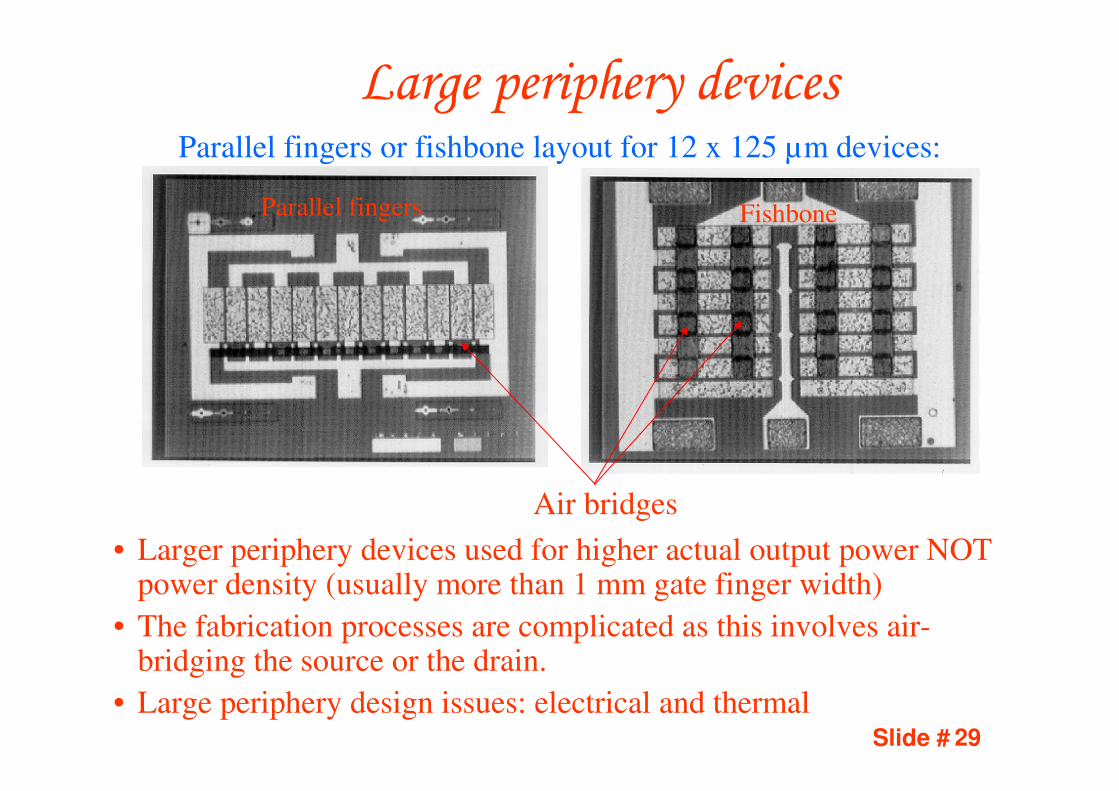
Large periphery devices
• Larger periphery devices used for higher actual output power NOTpower density (usually more than 1 mm gate finger width)
• The fabrication processes are complicated as this involves air-bridging the source or the drain.
• Large periphery design issues: electrical and thermal
Parallel fingers Fishbone
Parallel fingers or fishbone layout for 12 x 125 µm devices:
Air bridges
Slide # 30
Design issues for large periphery devices
Electrical issues:
• The voltage drop along the gate length causes lower PAE
• Phase difference at the gate fingers reduce overall PAE
• Finite Ron reduces PAE. This becomes severe in presence of
trapping as Ron increases
Thermal issues:
• Device heating is a problem at higher output power, since
power wasted is also larger
• The maximum possible output power depends on the
conductivity of the substrates. SiC substrates are commonly
used. Thinned sapphire substrates have also been used.
• The number of gate fingers as well as the gate finger pitch
determine the maximum temperature rise in a device.
Slide # 31
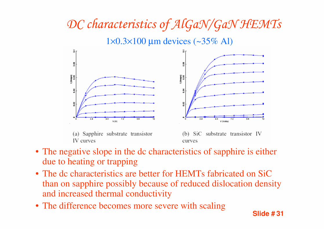
DC characteristics of AlGaN/GaN HEMTs
• The negative slope in the dc characteristics of sapphire is either due to heating or trapping
• The dc characteristics are better for HEMTs fabricated on SiCthan on sapphire possibly because of reduced dislocation densityand increased thermal conductivity
• The difference becomes more severe with scaling
1×0.3×100 µm devices (~35% Al)

Slide # 32
RF performance
1 10 1000
10
20
30
h21, U
PG
(d
B)
h21
UPG
f (GHz)
• ft of 22GHz and fmax of 40GHz were
obtained from a 0.7um-gate-length
HEMT at drain bias of 10V and drain
current of 240mA/mm.
• On sapphire substrate.
• No SiN passivation.
• 3.4W/mm with peak PAE 32% was
obtained at 10GHz when VD=15V and
ID=230mA/mm.
0 5 10 15 20 25
5
10
15
20
25
30
3.4W/mm
PA
E (
%)
Pin (dBm)
Po
ut
(dB
m),
Gain
(d
B) P
out
Gain
PAE
0
10
20
30
40
50
60
Small signal Large signal

Slide # 33
RF performance
1 10 1000
10
20
30
40
h21, U
PG
(d
B)
Frequency (GHz)
h21
UPG
• ft of 21GHz and fmax of 39GHz were
obtained from a 0.7um-gate-length
HEMT at drain bias of 15V and drain
current of 280mA/mm.
• On SiC substrate
• 12W/mm with a peak PAE of 44% was
obtained at 4GHz at VD=50V,
ID=270mA/mm
Small signal Large signal
0 5 10 15 20
10
15
20
25
30
35
44%
12W/mm
PA
E (
%)
Pin (dBm)
Po
ut
(dB
m),
Gain
(d
B) P
out
Gain
PAE
0
10
20
30
40
50