high frequency bjt model & cascode bjt amplifierese319/lecture_notes/lec_10... ·...
TRANSCRIPT

ESE319 Introduction to Microelectronics
1Kenneth R. Laker, update 01Oct14 KRL
High Frequency BJT Model & Cascode BJT Amplifier

ESE319 Introduction to Microelectronics
2Kenneth R. Laker, update 01Oct14 KRL
Gain of 10 Amplifier – Non-ideal Transistor
Gain starts dropping at > 1MHz.
Why!Because of internal transistorcapacitances that we have ignoredin our low frequency and mid-band models.
C in
RS
R1
R2
RC
RE
v s
V CC

ESE319 Introduction to Microelectronics
3Kenneth R. Laker, update 01Oct14 KRL
Sketch of Typical Voltage Gain Response for a CE Amplifier
∣Av∣dB
f Hz(log scale)f L f H
LowFrequency
BandDue to external blocking and by-pass capacitors.
Internal C's o.c.
MidbandALL capacitances are neglected, i.e. External C's s.c. Internal C's o.c.
3dB
20 log10∣Av∣dB
HighFrequency
Band
Due to BJT parasitic capacitors Cπ and Cµ. External C's s.c.
BW = f H− f L≈ f H GBP=∣Av−mid∣BW

ESE319 Introduction to Microelectronics
4Kenneth R. Laker, update 01Oct14 KRL
High Frequency Small-signal Model (Fwd. Act.)C
C
r x
Two capacitors and a resistor added to mid-band small signal model.● base-emitter capacitor, Cµ
● base-collector capacitor, Cπ
● resistor, rx, representing the base terminal resistance (rx << rπ); ignored in hand calculations.
vbe

ESE319 Introduction to Microelectronics
5Kenneth R. Laker, update 01Oct14 KRL
High Frequency Small-signal Model (Fwd. Act.)
C de=g mF=I C
V TF
Cde = base-charging (diffusion) cap
τF = forward-base transit time
SPICE/MultiSimCJC = C
µ0
CJE = Cje0
TF = τF
RB = rx
C
C
r x
C=C0
1V CB
0cb
m
vbe
Non-linear, voltage controlled
C je=C je0
1V EB
0eb
m
C≈2C 0
C=C deC je≈C de2C je 0≈C de
m = junction grading coefficient 0.2 to 0.5)
C=i
d vdtNote
ESE319 Introduction to Microelectronics
6Kenneth R. Laker, update 01Oct14 KRL
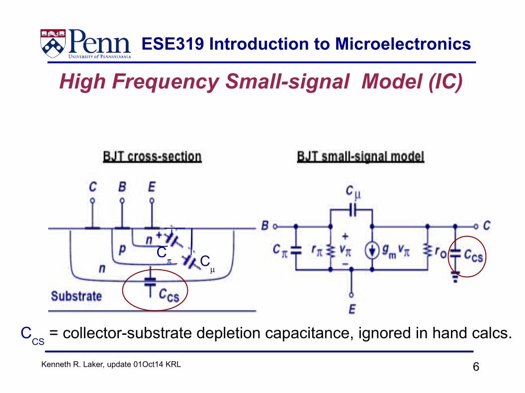
High Frequency Small-signal Model (IC)
Cµ
Cπ
CCS
= collector-substrate depletion capacitance, ignored in hand calcs.

ESE319 Introduction to Microelectronics
7Kenneth R. Laker, update 01Oct14 KRL
High Frequency Small-signal ModelThe transistor parasitic capacitances have a strong effect on circuit high frequency performance!
● Cπ attenuates base signal, decreasing vbe since XCπ → 0 (short circuit)
at very high-frequencies.●
● As we will see later; Cµ is principal cause of gain loss at high-frequencies. At the base base-collector Cµ looks like a capacitor of value k Cµ between base-emitter, where k > 1 and may be >> 1.
● This phenomenon is called the Miller Effect.
C
C
r x

ESE319 Introduction to Microelectronics
8Kenneth R. Laker, update 01Oct14 KRL
Prototype Common Emitter Circuit
High frequency small-signal ac model
At high frequencies large blocking and bypass
capacitors are “short circuits”
vs
RC
RE
V CC
RB
V B
RS C in
Cbyp
vo
vs
RS
RB RC
voc
e
b
r C
C
gm vbevbe
+
-

ESE319 Introduction to Microelectronics
9Kenneth R. Laker, update 01Oct14 KRL
Multisim Simulation
vs
RS
RB RC
voc
e
b
r C
C
gm vbe
50
50k 5.1k
2 pF
12 pF2.5 k 40mS vbe
Mid-band gain @ 100 kHz
Gain @ 8.69 MHz
vbe
Av−mid=−gm RC=−204 46 dB@ 180o

ESE319 Introduction to Microelectronics
10Kenneth R. Laker, update 01Oct14 KRL
vs
RS
RB RC
voc
e
b
r C
C
gm vbe
Introducing the Miller Effect
The feedback connection of between base-collector causes it to appear in the amplifier like a large capacitor between the base-emitter terminals. This phenomenon is called the “Miller effect” and capacitor multiplier “1 – K ” acting on equals the CE amplifier mid-band gain, i.e. .
NOTE: CB and CC amplifiers do not suffer from the Miller effect, since in these amplifiers, one side of is connected directly to ground.
C
C
K=Av−mid=−g m RC
1−K C
C
vbe
ESE319 Introduction to Microelectronics
11Kenneth R. Laker, update 01Oct14 KRL
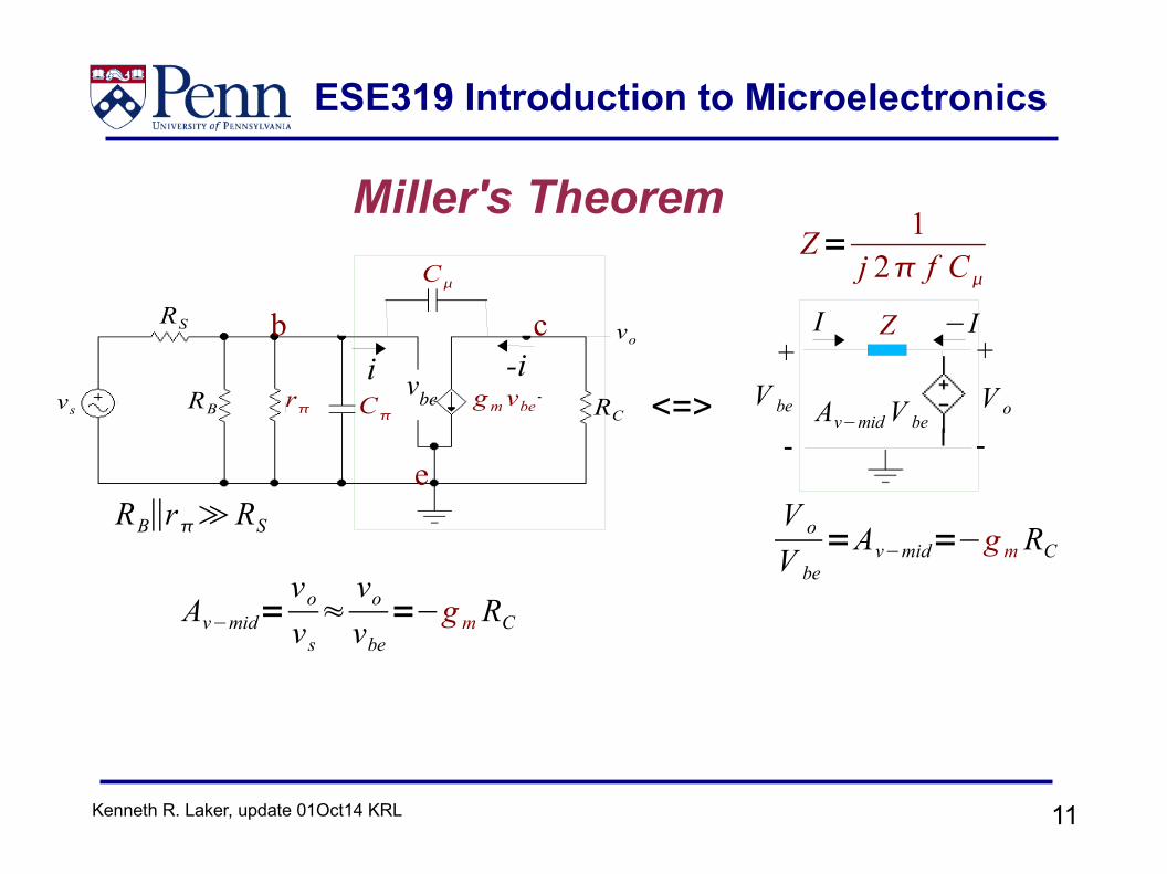
Miller's Theorem
vs
RS
RB RC
voc
e
b
r C
C
gm vbe
Av−mid=vo
vs≈
vo
vbe=−g m RC
I+ +
- -
Z
V be V o
−I
Av−mid V be
V o
V be=Av−mid=−g m RC
Z= 1j 2 f C
<=>
RB∥r≫RS
-ii vbe
ESE319 Introduction to Microelectronics
12Kenneth R. Laker, update 01Oct14 KRL
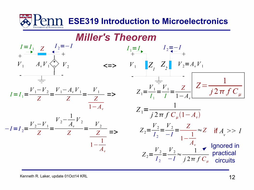
Miller's Theorem
I= I 1=V 1−V 2
Z=
V 1−Av V 1
Z=
V 1
Z1−Av
=>
Z 2=V 2
I 2=
V 2
−I=
Z
1− 1Av
≈Z=>
+ +
- -
I 1= I I 2=−I
V 1 V 2=Av V 1<=>
if Av >> 1
Z1
Z2
Z 1=1
j 2 f C1−Av
−I=I 2=V 2−V 1
Z=
V 2−1Av
V 2
Z=
V 2
Z
1− 1Av
I= I 1
+ +
- -
Z
V 1 V 2
I 2=−I
Av V 1
Z 2=V 2
I 2=
V 2
−I≈
1j 2 f C
Ignored in practical circuits
Z 1=V 1
I 1=
V 1
I=
Z1−Av
ESE319 Introduction to Microelectronics
13Kenneth R. Laker, update 01Oct14 KRL
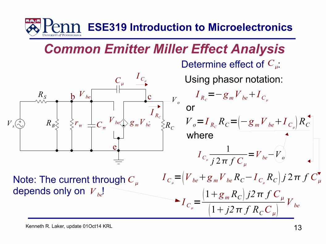
Common Emitter Miller Effect Analysis
V o=I RCRC=−g mV beI C RC
Using phasor notation:I RC
=−gmV beI C
or
Determine effect of :C
where
Note: The current through depends only on !
C
V be
V s
RS
RB RC
V oc
e
b
r C
C
gmV be
I C
I RC
V be
I C =V beg mV be RC− I C
RC j 2 f C
V be
I C
1j 2 f C
=V be−V o
I C =
1gm RC j2 f C
1 j2 f RC C V be

ESE319 Introduction to Microelectronics
14Kenneth R. Laker, update 01Oct14 KRL
Common Emitter Miller Effect Analysis II
I C =
1gm RC j2 f C
1 j2 f RC C V be≈ 1gm RC j2 f CV be= j2 f C eq V be
From slide 13:
Miller Capacitance Ceq: C eq=1gm RC C=1−Av C
V s
RS
RB RC
V oc
e
b
r C
C
gmV be
I C
I RC
V be
2 f RC C ≪1
vbeI C =
1gm RC j2 f C
1 j2 f RC C V be
ESE319 Introduction to Microelectronics
15Kenneth R. Laker, update 01Oct14 KRL
V s
RS
RB RC
V oc
e
b
r C
C
gmV be
I C
I RC
V be
V s
RS
RB RC
V oc
e
b
r C
C
g mV be
I C
I RC
V be
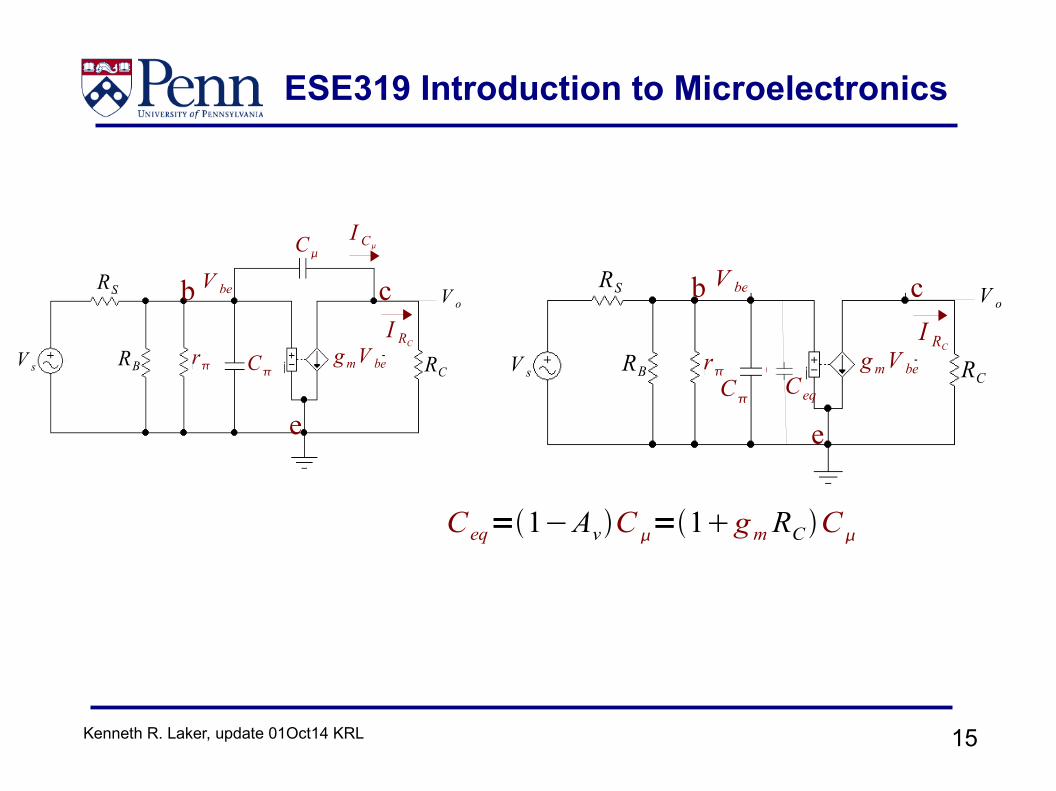
C
C eq=1−AvC =1gm RC C
C eq

ESE319 Introduction to Microelectronics
16Kenneth R. Laker, update 01Oct14 KRL
Common Emitter Miller Effect Analysis III
C eq=1gm RC C
For our example circuit (Cµ = 2 pF):
1gm RC=10.040⋅5100=205
C eq=205⋅2 pF≈410 pF

ESE319 Introduction to Microelectronics
17Kenneth R. Laker, update 01Oct14 KRL
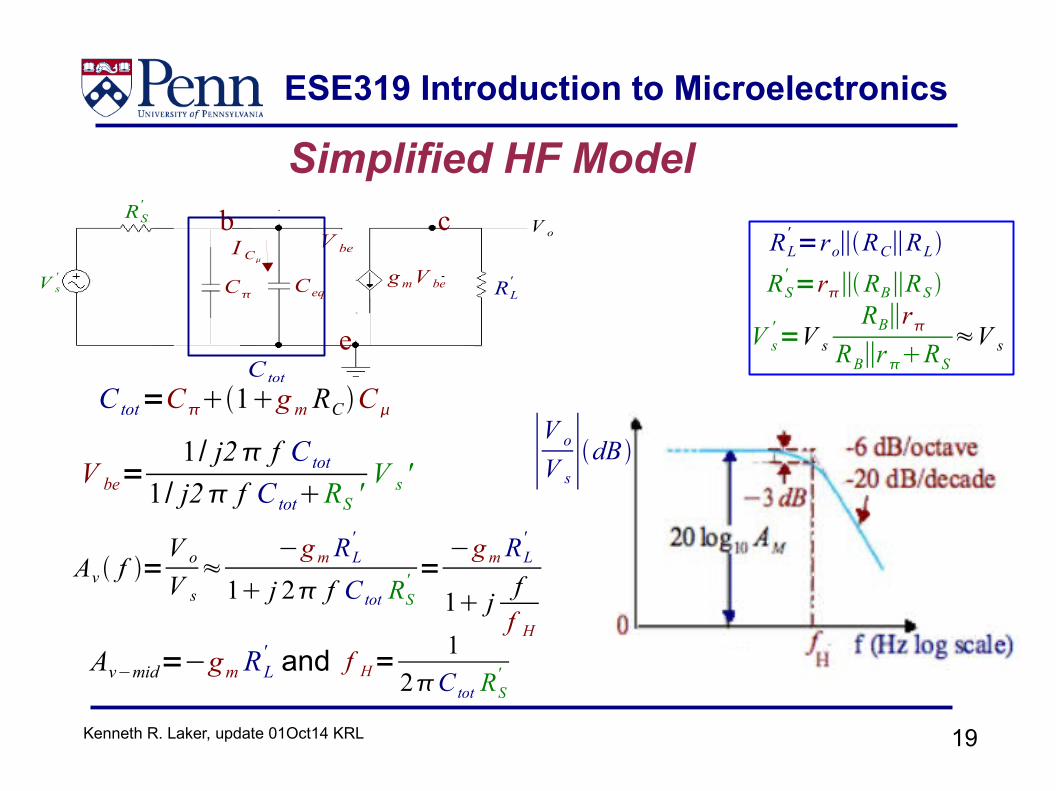
Simplified HF Model
V s' =V s
RB∥r
RB∥rRS
RS' =r∥RB∥RS
RL' =ro∥RC∥RL
V s'
RS'
RB
V oc
e
b
r C
C
gmV be
I CV be
RL'
V s
RS
RB
V oc
e
b
r C
C
gmV be
I CV be
RLRCro
Thevenin Equiv.
vbe
vbe

ESE319 Introduction to Microelectronics
18Kenneth R. Laker, update 01Oct14 KRL
Simplified HF Model
V s'
RS'
RB
V oc
e
b
r C
C
gmV be
I C
RL'
V be
C eq=1g m RC C
V s'
RS'
RB
V oc
e
r CeqgmV be RL
'
b
C
V beI C
C tot
Miller's Theorem
C tot=CC eq
RL' =ro∥RC∥RL
RS' =r∥RB∥RS
V s' =V s
RB∥r
RB∥rRS
ESE319 Introduction to Microelectronics
19Kenneth R. Laker, update 01Oct14 KRL
V s'
RS'
RB
V oc
e
r C eqgmV be RL
'
b
C
V beI C
C tot
Simplified HF Model
C tot=C1g m RCC
∣V o
V s∣dB
Av f =V o
V s≈
−g m RL'
1 j 2 f C tot RS' =
−gm RL'
1 j ff H
Av−mid=−gm RL' and f H=
12C tot RS
'
RL' =ro∥RC∥RL
RS' =r∥RB∥RS
V s' =V s
RB∥r
RB∥rRS≈V s
V be=1/ j2 f C tot
1/ j2 f C totRS 'V s '

ESE319 Introduction to Microelectronics
20Kenneth R. Laker, update 01Oct14 KRL
Multisim Simulation
vs
RS
RB RC
voc
e
b
r C
C
gm vbe
50
50k 5.1 k
2 pF
12 pF2.5 k 40 mS vbe Mid-band gain @ 100 kHz
Gain @ 8.69 MHz
vbe
Av−mid=−gm RC=−204 46 dB@ 180o
C tot=12 pF205⋅2 pF≈422 pF
f H≈ f −3dB=1
2C tot RS' ≈
12422 pF 50
≈7.54 MHz

ESE319 Introduction to Microelectronics
21Kenneth R. Laker, update 01Oct14 KRL
Frequency-dependent “beta”
I b= 1r
j2 f CCV b
short-circuit current
where r x≈0 (ignore rx)@ node B':
V bj2π f C
µV
bI
C = (g
m – j2π f C
µ)V
b
gm V b
0
The relationship ic = βib does not apply at high frequencies f ≥ fH!Using the relationship – ic = f (V
b ) – find the new relationship between ib and ic. For ib (using phasor notation (I
x=Ix (jf) & V
x=Vx (jf))
for frequency domain analysis):

ESE319 Introduction to Microelectronics
22Kenneth R. Laker, update 01Oct14 KRL
I b= 1r
j2 f CCV b I c=gm− j2 f CV b
Leads to a new relationship between the Ib and Ic:
jf =I c
I b=
gm− j2 f C
1r
j2 f CC
(ignore ro)@ node C:
Frequency-dependent “beta”
gm V b
V bj2π f C
µV
bI
C = (g
m – j2π f C
µ)V
b
∞
β(jf) h→ fe

ESE319 Introduction to Microelectronics
23Kenneth R. Laker, update 01Oct14 KRL
Frequency Response of “beta”
jf =gm− j2 f C
1r
j2 f CC
jf =gm− j2 f C r
1 j2 f CC r
jf =1− j2 f
C
g mg m r
1 j2 f CC r
For 2 f low
C
gm≪1≤ 1
10
and 2 f low CC r≪1≤ 110
jf =gm r=
gm=I C
V Tr=
V T
I C
f = f low
multiplying N&D by rπ
factor N to isolate gm
s.t.

ESE319 Introduction to Microelectronics
24Kenneth R. Laker, update 01Oct14 KRL
Frequency Response of “beta” cont.
jf =1− j2 f
C
gmg m r
1 j2 f CC r
=1− j f
f z 1 j f
f g m r=
1− j ff z
1 j ff
f =1
2CC r
=g m
2CC the upper: f z=
12C / gm
=g m
2C
Hence, the lower break frequency or – 3dB frequency is fβ
f z≫ f where
f
f dB
f z
f
20log10
ESE319 Introduction to Microelectronics
25Kenneth R. Laker, update 01Oct14 KRL
Frequency Response of “beta” cont.
For the range where: s.t. f f f z
We consider the frequency-dependent numerator term tobe 1 and focus on the response of the denominator:
Using Bode plot concepts, for the range where: f f
jf =gm r=
jf ≈gm r
1 j ff
=
1 j ff
∣1− j f / f z∣≈1
f f f z
ESE319 Introduction to Microelectronics
26Kenneth R. Laker, update 01Oct14 KRL
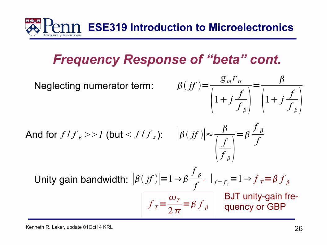
Frequency Response of “beta” cont.
jf =gm r
1 j ff
=
1 j ff
∣ jf ∣≈
ff
=f
f
Neglecting numerator term:
Unity gain bandwidth: ∣ jf ∣=1⇒f
f¿¿ f = f T
=1⇒ f T= f
f T=T
2= f
And for >>1 (but < ):f / f f / f z
BJT unity-gain fre-quency or GBP
|
ESE319 Introduction to Microelectronics
27Kenneth R. Laker, update 01Oct14 KRL
Frequency Response of “beta” cont.
=1
CC r
=1012⋅10−3
122⋅2.5=28.57⋅106 rps
z=gm
C
=40⋅10−3⋅1012
2Hz=20⋅109 rps
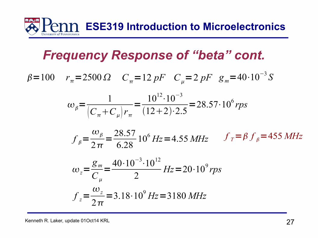
=100 r=2500 C=12 pF C=2 pF gm=40⋅10−3 S
f =
2=
28.576.28
106 Hz=4.55 MHz
f z=z
2=3.18⋅109 Hz=3180 MHz
f T= f =455 MHz

ESE319 Introduction to Microelectronics
28Kenneth R. Laker, update 01Oct14 KRL
“beta” Bode Plot(dB)
fTf
β
|β(jf)| vs. Frequency|β(jf)| (dB)
f (MHz)

ESE319 Introduction to Microelectronics
29Kenneth R. Laker, update 01Oct14 KRL
Multisim Simulation
Insert 1 ohm resistors – we want to measure a current ratio.
Ib
Ic
jf =I c
I b=
gm− j2 f C
1r
j2 f CC
mS
v-pi
v-pi
1 Ohm
1 OhmVc
Vb

ESE319 Introduction to Microelectronics
30Kenneth R. Laker, update 01Oct14 KRL
Simulation Results
Low frequency |β(jf)|
Unity Gain frequency about 440 MHz.
f T= f =455 MHzTheory:

ESE319 Introduction to Microelectronics
31Kenneth R. Laker, update 01Oct14 KRL
The Cascode Amplifier● A two transistor amplifier used to obtain simultaneously:
1. Reasonably high input impedance.2. Reasonable voltage gain.3. Wide bandwidth.
● None of the conventional single transistor designs will satisfy all of the criteria above. ● The cascode amplifier will satisfy all of these criteria. ● A cascode is a CE Stage cascaded with a CB Stage.
(Historical Note: the cascode amplifier was a cascade of groundedcathode and grounded grid vacuum tube stages – hence thename “cascode,” which has remained in modern terminology.)

ESE319 Introduction to Microelectronics
32Kenneth R. Laker, update 01Oct14 KRL
The Cascode Amplifier
f f min
ac equivalent circuit
ib2
ie2
ic2
ic1
ib1
ie1
Rin1=ve1
i e1=
vc2
ic2=low≈r e1
RB
RB=R2∥R3
CE Stage CB Stage
vs
Rs
RE
RC
vo
CE Stage
Q2
Q1RS
v-outi B1
i B2
i E1 iC2
i E2vs
R1
R2
R3 R
E
RC
Rs
Cin
vO
V CC
Cbyp
CB Stage
CE Stage
B1 C1
E1
C2C2
E2B2
Q1
Q2RS
iC1
Comments:1. R1, R2, R3, and RC set the bias levels for both Q1 and Q2.2. Determine RE for the desired voltage gain.3. Cin and Cbyp are to act as “open circuits” at dc and act as near “short circuits” at all operating frequencies .

ESE319 Introduction to Microelectronics
33Kenneth R. Laker, update 01Oct14 KRL
CE Amplifier CB Amplifier
Voltage Gain (AV) moderate (-RC/R
E) High (R
C/(R
s + r
e))
Current Gain (AI) High (β) low (about 1)
Input Resistance High (RB||βR
E) low (r
e)
Output Resistance High (RC||r
o) High (R
C||r
o)
CE and CB Amplifier Feature Review
Important for Cascode

ESE319 Introduction to Microelectronics
34Kenneth R. Laker, update 01Oct14 KRL
Cascode Mid-Band Small Signal Model
RB=R2∥R3
ic1
ic2
ie1
ie2
ib2
ib1
RB
Rin1=low
vs
Rs
RE
RC
r2
r1 g m v1
g m v 2
voCB Stage
CE Stage
v1
v 2
C1
B1
E1B2
E2
C2
gm1
vbe1
vbe1
vbe2 g
m2v
be2RS
v-outi B1
i B2
i E1 iC2
i E2vs
R1
R2
R3 R
E
RC
Rs
Cin
vO
V CC
Cbyp
CB Stage
CE Stage
B1 C1
E1
C2C2
E2B2
Q1
Q2RS
iC1
RB=R2∥R3
ASSUME: Q1 = Q2; e.g. β's identical, and both Forward Active

ESE319 Introduction to Microelectronics
35Kenneth R. Laker, update 01Oct14 KRL
Cascode Small Signal Analysis
ie1=ic2
c. Hence, both stages have about same collector current and same gm, r
e, r
π.
ib1=ie1
1=
ic2
1
OBSERVATIONS
ic1≈ic2
gm1=g m2=g mre1=r e2=r e
r1=r2=r
ic1
ic2
ie1
ie2
ib2
ib1
RB
Rin1=low
vs
Rs
RE
RC
r2
r1 g m v1
g m v 2
voCB Stage
CE Stage
v1
v 2
C1
B1
E1B2
E2
C2
gm1
vbe1
vbe1
vbe2 g
m2v
be2RS
a. The emitter current of the CB Stage is the collector current of the CE Stage. (This also holds for the dc bias currents.)
1. Show reduction in Miller effect2. Evaluate small-signal voltage gain
b. The base current of the CB Stage is:
I C1≈ I C2
ESE319 Introduction to Microelectronics
36Kenneth R. Laker, update 01Oct14 KRL
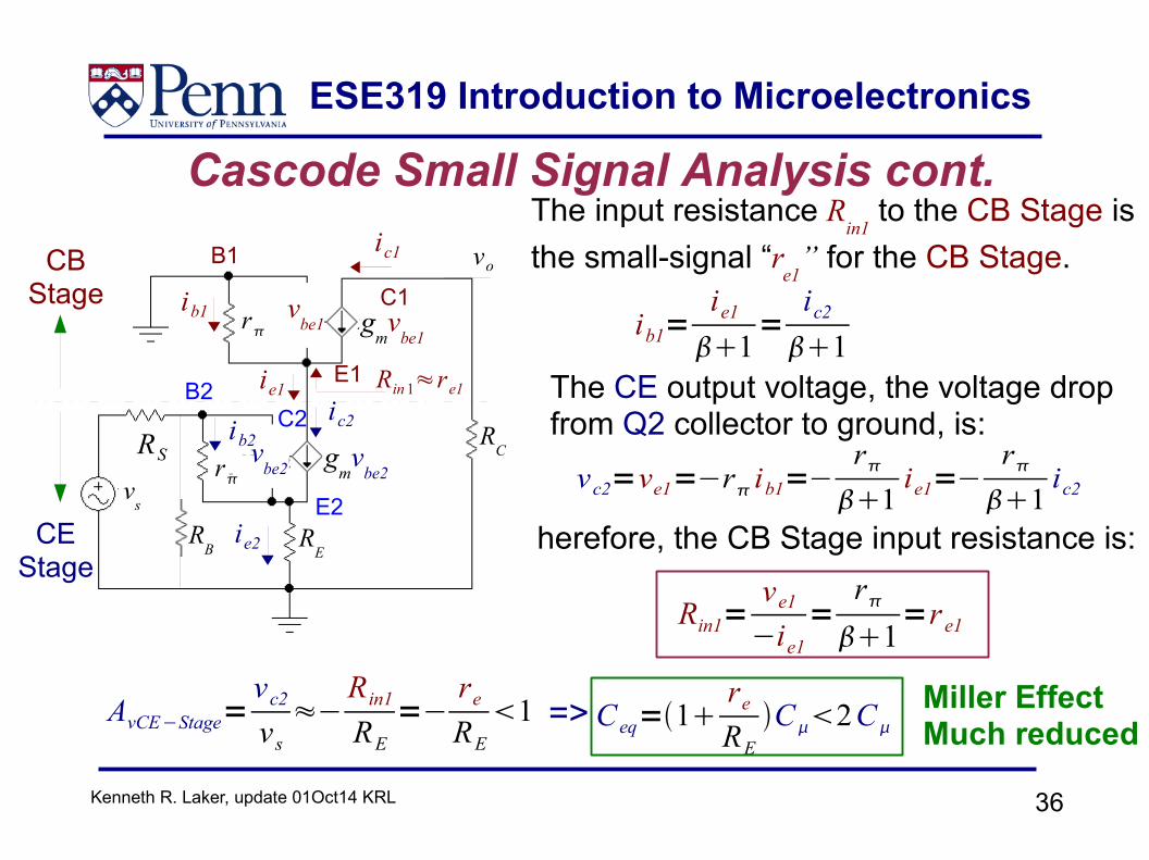
Cascode Small Signal Analysis cont.
ib1=ie1
1=
ic2
1The CE output voltage, the voltage drop from Q2 collector to ground, is:
Therefore, the CB Stage input resistance is:
Rin1=ve1
−ie1=
r
1=r e1
vc2=ve1=−r ib1=−r
1ie1=−
r
1ic2
AvCE−Stage=vc2
vs≈−
Rin1
RE=−
re
RE1 => C eq=1
re
REC2C
ic1
ic2
ie1
ie2
ib2
ib1
RB
vs
Rs
RE
RC
r
r g m v1
g m v 2
voCB Stage
CE Stage
v1
v 2
C1
B1
E1B2
E2
C2
gmv
be1v
be1
vbe2 g
mv
be2RS
Rin 1≈re1
The input resistance Rin1
to the CB Stage is the small-signal “r
e1” for the CB Stage.
Miller EffectMuch reduced

ESE319 Introduction to Microelectronics
37Kenneth R. Laker, update 01Oct14 KRL
Cascode Small Signal Analysis - cont.
ib2≈vs
RS∥RBr1RE
ic2= ib2≈vs
RS∥RBr1RE≈
vs
1RE
Now, find the CE collector current in terms of the input voltage v
s:
1RE≫RS∥RBrfor bias insensitivity:
ic1≈ic2Recall
OBSERVATIONS:1. Voltage gain A
v is about the same as a stand-along CE Amplifier.
2. HF cutoff is much higher then a CE Amplifier due to the reduced Ceq.
v s Av=vo
v s≈−RC
RE
vbe1
vbe2
g m vbe1
g m vbe2vbe2
vbe1
RS
ic1≈ie1=ic2≈ie2
Rin 1≈re1
ic1
ib1
ie1
gmv
be1
gmv
be2
ie2
ic2ib2
ic2≈v s
RE
vo≈−ic2 RC

ESE319 Introduction to Microelectronics
38Kenneth R. Laker, update 01Oct14 KRL
V s'
RS'
RB
V oc
e
r C eqgmV be RL
'
b
C
V beI C
C tot
C tot=C1g m RC C
∣V o
V s∣dB
Common Emitter Stage
Cascode Stage
C tot=C1r e
REC
.2C
f H=1
2C tot RS' ⇒ f H Cascode ≫ f H CE

ESE319 Introduction to Microelectronics
39Kenneth R. Laker, update 01Oct14 KRL
Cascode Biasing
Rin1=r e=V T / I E1
IE1 IC2
IE2
Rin1=low
1. Choose IE1 – make it relatively large to reduce to push out HF break frequencies.
I1
o.c.
o.c.
vO
C in
C B 2. Choose RC for suitable voltage swing V
C1 and RE for desired gain.
3. Choose bias resistor string such that its current I
1 is about 0.1 of the collector
current IC1
.
4. Given RE, IE2 and VBE2
= 0.7 V calc. R3.
5. Need to also determine R1 & R
2.
RS
Q1
Q2
I E2=I C2=I E1=1
I C1⇒ I C1=2 I E2≈ I E2
IC1

ESE319 Introduction to Microelectronics
40Kenneth R. Laker, update 01Oct14 KRL
Cascode Biasing - cont.
Since the CE-Stage gain is very small: a. The collector swing of Q2 will be small. b. The Q2 collector bias V
C2= V
B1 - 0.7 V.
6. Set
Since VCE2
= 1 V > VCE2sat
Q2 forward active. 7. Next determine R
2. Its drop V
R2 = 1 V
with the known current.
V B1−V B2=1V ⇒V CE2=1V
V CE2=V C2−V R e=V C2−V B2−0.7V
.=V B1−V B2=1V
I 1
.=V B1−0.7V −V B20.7V
VB2
VB1
VC2
I1
vOQ1
Q2
Rin 1≈re1
.=V B1−0.7V −V R eR2=
V B1−V B2
I 1
ESE319 Introduction to Microelectronics
41Kenneth R. Laker, update 01Oct14 KRL
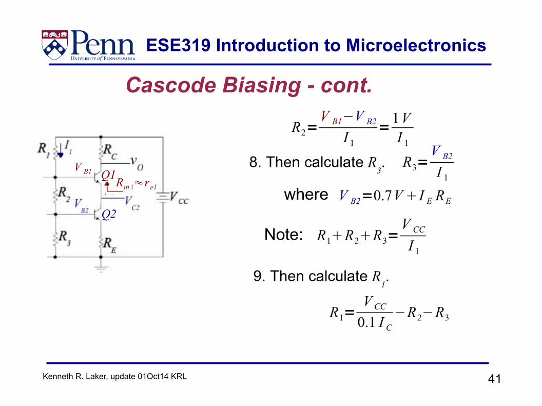
Cascode Biasing - cont.
8. Then calculate R3.
R2=V B1−V B2
I 1=1V
I 1
R3=V B2
I 1
where V B2=0.7V I E RE
R1R2R3=V CC
I 1Note:
9. Then calculate R1.
R1=V CC
0.1 I C−R2−R3
Q1
Q2
V B1
Rin 1≈re1

ESE319 Introduction to Microelectronics
42Kenneth R. Laker, update 01Oct14 KRL
Cascode Bias SummarySPECIFIED: A
v, V
CC, V
C1 (CB collector voltage);
SPECIFIED: fH => Ctot(re) => IE (or I
C) => re.
DETERMINE: RC, R
E, R
1, R
2 and R
3.
SET: RC=V C1
I C
RE=RC
∣Av∣
R1R2R3=V CC
I 1=
V CC
0.1 I C
V B1−V B2=1V ⇒V CE2=1V
R3=V B2
I 1=
0.7VI E RE
0.1 I C
R2=V B1−V B2
I 1=
1V0.1 I C
R1=V CC
0.1 I C−R2−R3
STEP1:
STEP2:
STEP3:STEP3:
STEP4:
Q2
Q1
I C2= I E1≈ I C1≈ I E2=I C
V B1
Rin 1≈re1

ESE319 Introduction to Microelectronics
43Kenneth R. Laker, update 01Oct14 KRL
Cascode Amp
Cascode Bias Example
Typical Bias Conditions
ICR
E
ICRC
ICRE+0.7
VCE2=1
VCE1=ICRC–1–ICRE
1.0
VCC-ICRE-1.7
=12 V
I E2≈ I C2= I E1≈ I C1⇒ I C1≈ I E2
=12 V
RC
RE
V CE1=V CC−I C RC−V CE2−I C RE
V C1Q1 Q1
Q2 Q2
R1

ESE319 Introduction to Microelectronics
44Kenneth R. Laker, update 01Oct14 KRL
Cascode Bias Example cont.
1. Choose IE1 – to set re.Let re = 5Ω => .
2. Set desired gain magnitude. For exampleif A
V = -10, then RC/RE = 10.
3. Since the CE stage gain is very small,VCE2 can be small, i.e. V
CE2 = VB1 – VB2 = 1 V.
I E1=0.025V /r e=5mAV CE1=V CC− I C RC−1− I C RE
Q2
Q1

ESE319 Introduction to Microelectronics
45Kenneth R. Laker, update 01Oct14 KRL
Cascode Bias Example cont.
r e=5 ∣Av∣=RC
RE=10
RC=V CC−V C1
5⋅10−3 A= 5V
5⋅10−3 A=1000
RE=RC
∣Av∣=
RC
10=100
Determine RC for VC1
= 7V .
V CC=12V
V CE1=V CC− I C RC−1− I C RE
Q1
Q2
V C1=7VSpecs:
=100
IE1=0.025V / re=5 mA
ESE319 Introduction to Microelectronics
46Kenneth R. Laker, update 01Oct14 KRL
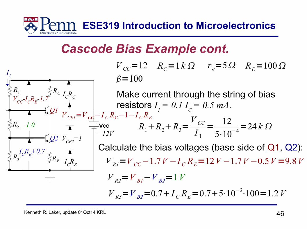
Cascode Bias Example cont.V CC=12 RC=1k RE=100
Make current through the string of biasresistors I
1 = 0.1 I
C = 0.5 mA.
R1R2R3=V CC
I 1= 12
5⋅10−4=24 k
V R3=V B2=0.7 I C RE=0.75⋅10−3⋅100=1.2 V
ICRE
ICRC
VCE2=1
1.0
V R1=V CC−1.7V −I C RE=12V −1.7V −0.5V =9.8 V
VCE1=ICRC–1–ICRE
VCC-ICRE-1.7
ICRE+0.7
I1
=12V
RC
RE
R1
R2
R3
V CE1=V CC−I C RC−1− I C RE
Calculate the bias voltages (base side of Q1, Q2):
Q1
Q2
V R2=V B1−V B2=1V
r e=5=100

ESE319 Introduction to Microelectronics
47Kenneth R. Laker, update 01Oct14 KRL
Cascode Bias Example cont.
V CC=12 RC=1k
I C=5 mA RE=100
V B2=1.2V
V B1−V B2=1.0V
V B2=5⋅10−4 R3=1.2V
R3=2.4 k V B1−V B2=5⋅10−4 R2=1.0V
R2=2 k
R1=24000−2.400−2000=19.6 k
V B1
V B2C in
C B
R1R2R3=24 kRecall:
Q1
Q2RS
, , ,
, ,
RS
Recall for ac: RB=R2∥R3
RB=2 k ∥2.4 k =1.1 k

ESE319 Introduction to Microelectronics
48Kenneth R. Laker, update 01Oct14 KRL
V B1
V B2C in
C BQ1
Q2RS
Completed Design
R1=19.6 kR2=2 k R3=2.4 k
RS
RC=1k
RE=100
V C1=7 Vre=5⇒ I C=5mA
∣Av∣=RC
RE=10
f Hcascode=225.8 MHz
C tot=14.1 pF
.=C1.05C
If Cπ = 12 pF
Cµ = 2 pF
C tot=C1re
REC
f H=1
2C tot RS'
f HCE=94 MHzFor CE with |A
v| = 10
RB=R2∥R3=1.09 k ≪RE=10 k
=100
NOTE: