high-frequency semiconductors power devices
TRANSCRIPT
Semiconductor Company
High-Frequency
Semiconductors
Power Devices
The information contained herein is subject to change without notice. 021023_D
The information contained herein is presented only as a guide for the applications of our
products. No responsibility is assumed by TOSHIBA for any infringements of patents or
other rights of the third parties which may result from its use. No license is granted by
implication or otherwise under any patent or patent rights of TOSHIBA or others.
021023_C
TOSHIBA is continually working to improve the quality and reliability of its products.
Nevertheless, semiconductor devices in general can malfunction or fail due to their
inherent electrical sensitivity and vulnerability to physical stress.
It is the responsibility of the buyer, when utilizing TOSHIBA products, to comply with
the standards of safety in making a safe design for the entire system, and to avoid
situations in which a malfunction or failure of such TOSHIBA products could cause loss
of human life, bodily injury or damage to property.
In developing your designs, please ensure that TOSHIBA products are used within
specified operating ranges as set forth in the most recent TOSHIBA products
specifications.
Also, please keep in mind the precautions and conditions set forth in the “Handling
Guide for Semiconductor Devices,” or “TOSHIBA Semiconductor Reliability
Handbook” etc. 021023_A
The Toshiba products listed in this document are intended for usage in general
electronics applications (computer, personal equipment, office equipment, measuring
equipment, industrial robotics, domestic appliances, etc.).
These Toshiba products are neither intended nor warranted for usage in equipment that
requires extraordinarily high quality and/or reliability or a malfunction or failure of
which may cause loss of human life or bodily injury (“Unintended Usage”).
Unintended Usage include atomic energy control instruments, airplane or spaceship
instruments, transportation instruments, traffic signal instruments, combustion control
instruments, medical instruments, all types of safety devices, etc. Unintended Usage of
Toshiba products listed in this document shall be made at the customer’s own risk.
021023_B
The products described in this document may include products subject to the foreign
exchange and foreign trade laws. 021023_F
TOSHIBA products should not be embedded to the downstream products which are
prohibited to be produced and sold, under any law and regulations. 030519_Q
GaAs(Gallium Arsenide) is used in some of the products. The dust or vapor is harmful
to the human body. Do not break, cut, crush or dissolve chemically. 021023_J
© 2004 TOSHIBA CORPORATION
All Rights Reserved
Semiconductor Company
Preface
Thank you for choosing Toshiba semiconductor products. This is the
year 2004 edition of the databook entitled High-Frequency
Semiconductor Devices – Power Devices.
From this edition, the High-Frequency Semiconductor Devices is
published in separate volumes: High-Frequency Semiconductor Devices
– Diodes, High-Frequency Semiconductor Devices – Transistors, FETs
and Cell Packs, and High-Frequency Semiconductor Devices – Power
Devices. Please select the suitable databook for your application.
This databook is designed to be easily understood by engineers who
are designing Toshiba high-frequency small-signal devices into their
products for the first time. No special knowledge of these devices is
assumed - the contents includes basic information about the
high-frequency small-signal devices and the application fields in which
they are used. In addition, complete technical specifications facilitate
selection of the most appropriate high-frequency small-signal device for
any given application.
Toshiba are continually updating technical publications. Any comments
and suggestions regarding any Toshiba document are most welcome and
will be taken into account when subsequent editions are prepared. To
receive updates to the information in this databook, or for additional
information about the products described in it, please contact your
nearest Toshiba office or authorized Toshiba dealer.
March 2004

5
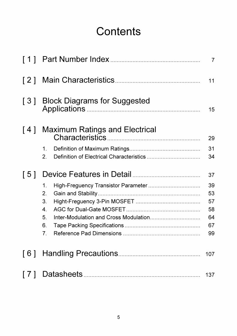
Contents
[ 1 ] Part Number Index ......................................................... 7
[ 2 ] Main Characteristics ...................................................... 11
[ 3 ] Block Diagrams for Suggested Applications ........................................................................ 15
[ 4 ] Maximum Ratings and Electrical Characteristics ........................................................... 29
1. Definition of Maximum Ratings............................................. 31
2. Definition of Electrical Characteristics .................................. 34
[ 5 ] Device Features in Detail ........................................... 37
1. High-Freguency Transistor Parameter ................................. 39
2. Gain and Stability................................................................. 53
3. Hight-Freguency 3-Pin MOSFET ......................................... 57
4. AGC for Dual-Gate MOSFET............................................... 58
5. Inter-Modulation and Cross Modulation................................ 64
6. Tape Packing Specifications ................................................ 67
7. Reference Pad Dimensions ................................................. 99
[ 6 ] Handling Precautions.................................................... 107
[ 7 ] Datasheets .......................................................................... 137
6
[ 8 ] Package Dimensions .................................................... 245
[ 9 ] List of Final-Phase Products..................................... 253
[ 10 ] List of Discontinued Products .................................. 257
[ 1 ] Part Number Index

[ 1 ] Part Number Index
9
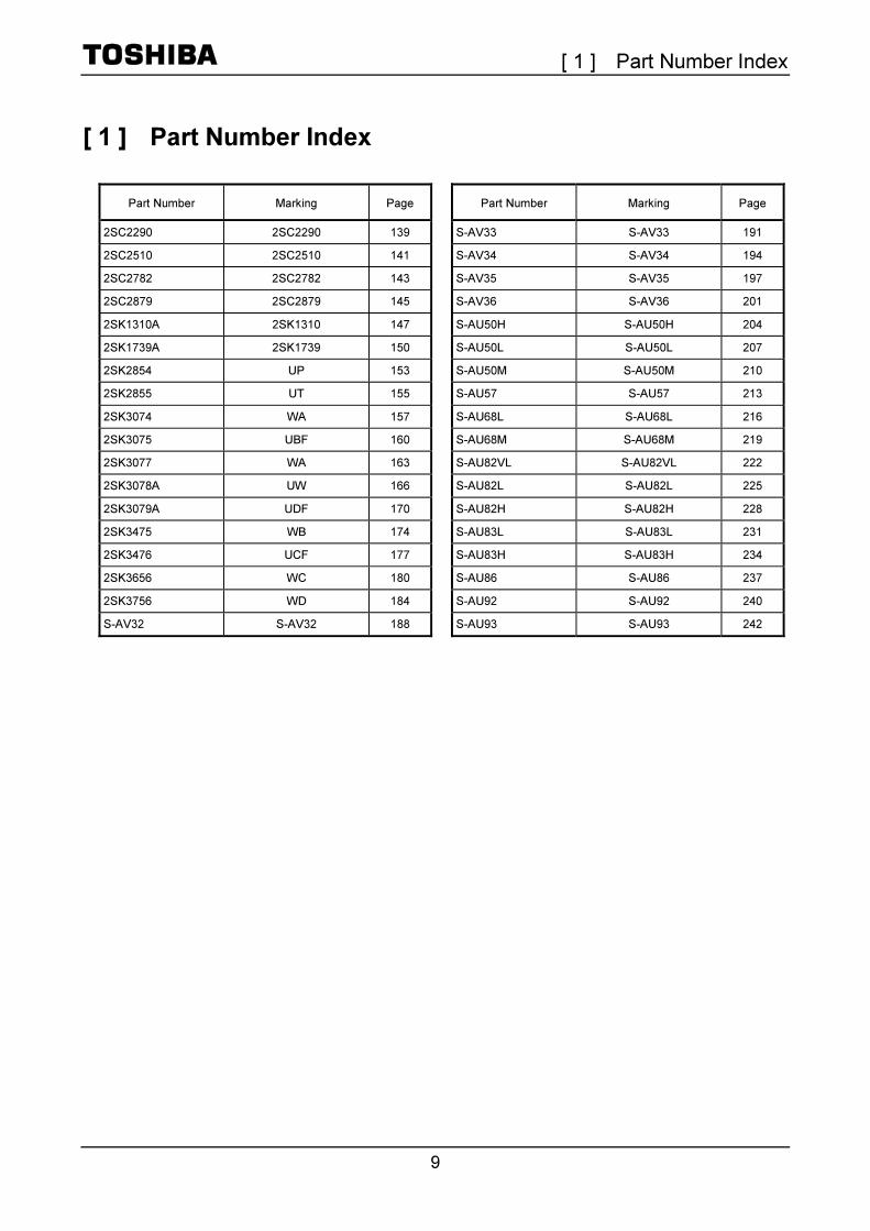
[ 1 ] Part Number Index
Part Number Marking Page
2SC2290 2SC2290 139
2SC2510 2SC2510 141
2SC2782 2SC2782 143
2SC2879 2SC2879 145
2SK1310A 2SK1310 147
2SK1739A 2SK1739 150
2SK2854 UP 153
2SK2855 UT 155
2SK3074 WA 157
2SK3075 UBF 160
2SK3077 WA 163
2SK3078A UW 166
2SK3079A UDF 170
2SK3475 WB 174
2SK3476 UCF 177
2SK3656 WC 180
2SK3756 WD 184
S-AV32 S-AV32 188
Part Number Marking Page
S-AV33 S-AV33 191
S-AV34 S-AV34 194
S-AV35 S-AV35 197
S-AV36 S-AV36 201
S-AU50H S-AU50H 204
S-AU50L S-AU50L 207
S-AU50M S-AU50M 210
S-AU57 S-AU57 213
S-AU68L S-AU68L 216
S-AU68M S-AU68M 219
S-AU82VL S-AU82VL 222
S-AU82L S-AU82L 225
S-AU82H S-AU82H 228
S-AU83L S-AU83L 231
S-AU83H S-AU83H 234
S-AU86 S-AU86 237
S-AU92 S-AU92 240
S-AU93 S-AU93 242

10

[ 2 ] Main Characteristics


[ 2 ] Main Characteristics
13
[ 2 ] Main Characteristics
1. Main Characteristics of High-Frequency Power Transistors
Maximum Ratings
(TC = 25°C) PO (W)
Test Conditions Application Part Number VCBO
(V)
PC
(TC = 25°C)
(W)
IC
(A)
Min
VCC
(V)
f
(MHz)
Pi
(W)
2SC2290 45 175 20 60PEP 12.5 28 4PEP
2SC2879 45 250 25 80PEP 12.5 28 8PEP
27 to 50 MHz
CB radio transmitter
HAM radio transmitter 2SC2510 60 250 20 150PEP 28 28 9PEP
175 MHz
Marine radio transmitter
HAM radio transmitter
Business-use radio transmitter
2SC2782 36 220 20 80 12.5 175 18
2. Main Characteristics of High-Frequency Power MOSFETs
Maximum Ratings
(TC = 25°C) PO
Test Conditions Application Part Number VDSS
(V)
PC
(TC = 25°C)
(W)
ID
(A)
Min
VDD
(V)
f
(MHz)
Pi
VHF 2SK1310A 100 250 12 190 W 50 230 10 W For TV broadcasting
UHF 2SK1739A 80 250 11 90 W 40 770 10 W
2SK2854 10 0.5 0.5 0.2 W 6 849 0.02 W For cellular phone
2SK2855 10 0.5 1 1.26 W 6 849 0.2 W
2SK3074 30 3 1 0.63 W 9.6 520 0.02 W For radio transmitter
2SK3075 30 20 5 7.5 W 9.6 520 0.5 W
For cellular phone 2SK3077 10 0.1 0.1 15.0dBmW 4.8 915 0dBmW
2SK3475 20 3 1 0.63 W 7.2 520 0.02 W For radio transmitter
2SK3476 20 20 3 7 W 7.2 520 0.5 W
2SK3078A 10 3 0.5 0.63 W 4.5 470 0.1 W
2SK3079A 10 20 3 2.24 W 4.5 470 0.1 W
2SK3656 7.5 3 0.5 0.5 W 3.6 470 0.02 W For FRS/GMRS
2SK3756 7.5 3 1 1.25 W 4.5 470 0.1 W
[ 2 ] Main Characteristics
14
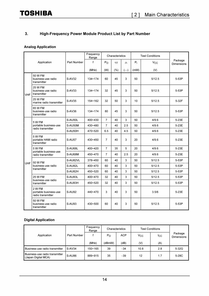
3. High-Frequency Power Module Product List by Part Number
Analog Application
Frequency
Range Characteristics Test Conditions
Application Part Number f
(MHz)
PO
(W)
ηT
(%)
ρi
(⎯)
Pi
(mW)
VCC
(V)
Package
Dimensions
50 W FM business-use radio transmitter
S-AV32 134~174 60 45 3 50 5/12.5 5-53P
25 W FM business-use radio transmitter
S-AV33 134~174 32 45 3 50 5/12.5 5-53P
25 W FM marine radio transmitter
S-AV35 154~162 32 50 3 10 5/12.5 5-32F
VHF
65 W FM business-use radio transmitter
S-AV36 134~174 80 45 3 50 5/12.5 5-53P
S-AU50L 400~430 7 40 3 50 4/9.6 5-23E
S-AU50M 430~480 7 40 2.5 50 4/9.6 5-23E 5 W FM portable business-use radio transmitter
S-AU50H 470~520 6.5 40 4.5 50 4/9.6 5-23E
5 W FM portable HAM radio transmitter
S-AU57 430~450 7 40 3 20 4/9.6 5-23E
S-AU68L 400~420 7 35 5 20 4/9.6 5-23E 5 W FM portable business-use radio transmitter S-AU68M 450~470 7 40 2.5 20 4/9.6 5-23E
S-AU82VL 378~450 60 40 3 50 5/12.5 5-53P
S-AU82L 400~470 60 40 3 50 5/12.5 5-53P 50 W FM business-use radio transmitter
S-AU82H 450~520 60 40 3 50 5/12.5 5-53P
S-AU83L 400~470 32 40 3 50 5/12.5 5-53P 25 W FM business-use radio transmitter S-AU83H 450~520 32 40 3 50 5/12.5 5-53P
2 W FM portable business-use radio transmitter
S-AU92 440~470 3 40 3 50 3.5/6 5-23E
UHF
50 W FM business-use radio transmitter
S-AU93 430~500 60 40 3 50 5/12.5 5-53P
Digital Application
Frequency
Range Characteristics Test Conditions
Application Part Number f
(MHz)
PO
(dBmW)
ACP
(dB)
VCC
(V)
ICC
(A)
Package
Dimensions
Business-use radio transmitter S-AV34 150~165 39 −34 10.8 2.8 5-32G
Business-use radio transmitter (Japan Digital MCA)
S-AU86 889~915 35 −39 12 1.7 5-28C

[ 3 ] Block Diagrams for
Suggested Applications

[ 3 ] Block Diagrams for Suggested Applications
17
[ 3 ] Block Diagrams for Suggested Applications
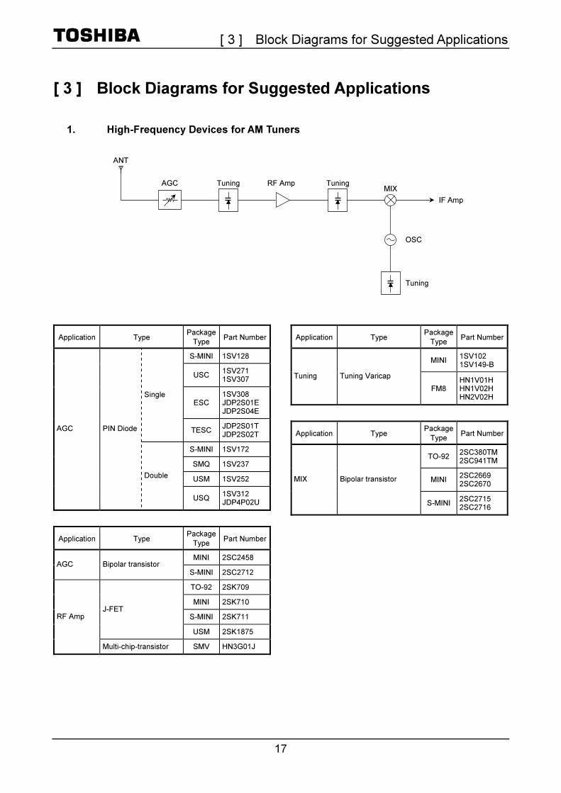
1. High-Frequency Devices for AM Tuners
Application Type Package
Type Part Number
S-MINI 1SV128
USC 1SV271 1SV307
ESC 1SV308 JDP2S01E JDP2S04E
Single
TESC JDP2S01T JDP2S02T
S-MINI 1SV172
SMQ 1SV237
USM 1SV252
AGC PIN Diode
Double
USQ 1SV312 JDP4P02U
Application Type Package
Type Part Number
MINI 2SC2458 AGC Bipolar transistor
S-MINI 2SC2712
TO-92 2SK709
MINI 2SK710
S-MINI 2SK711 J-FET
USM 2SK1875
RF Amp
Multi-chip-transistor SMV HN3G01J
Application Type Package
Type Part Number
MINI 1SV102 1SV149-B
Tuning Tuning Varicap
FM8 HN1V01H HN1V02H HN2V02H
Application Type Package
Type Part Number
TO-92 2SC380TM 2SC941TM
MINI 2SC2669 2SC2670
MIX Bipolar transistor
S-MINI 2SC2715 2SC2716
Tuning RF Amp Tuning
Tuning
MIX
IF Amp
OSC
AGC
ANT
[ 3 ] Block Diagrams for Suggested Applications
18
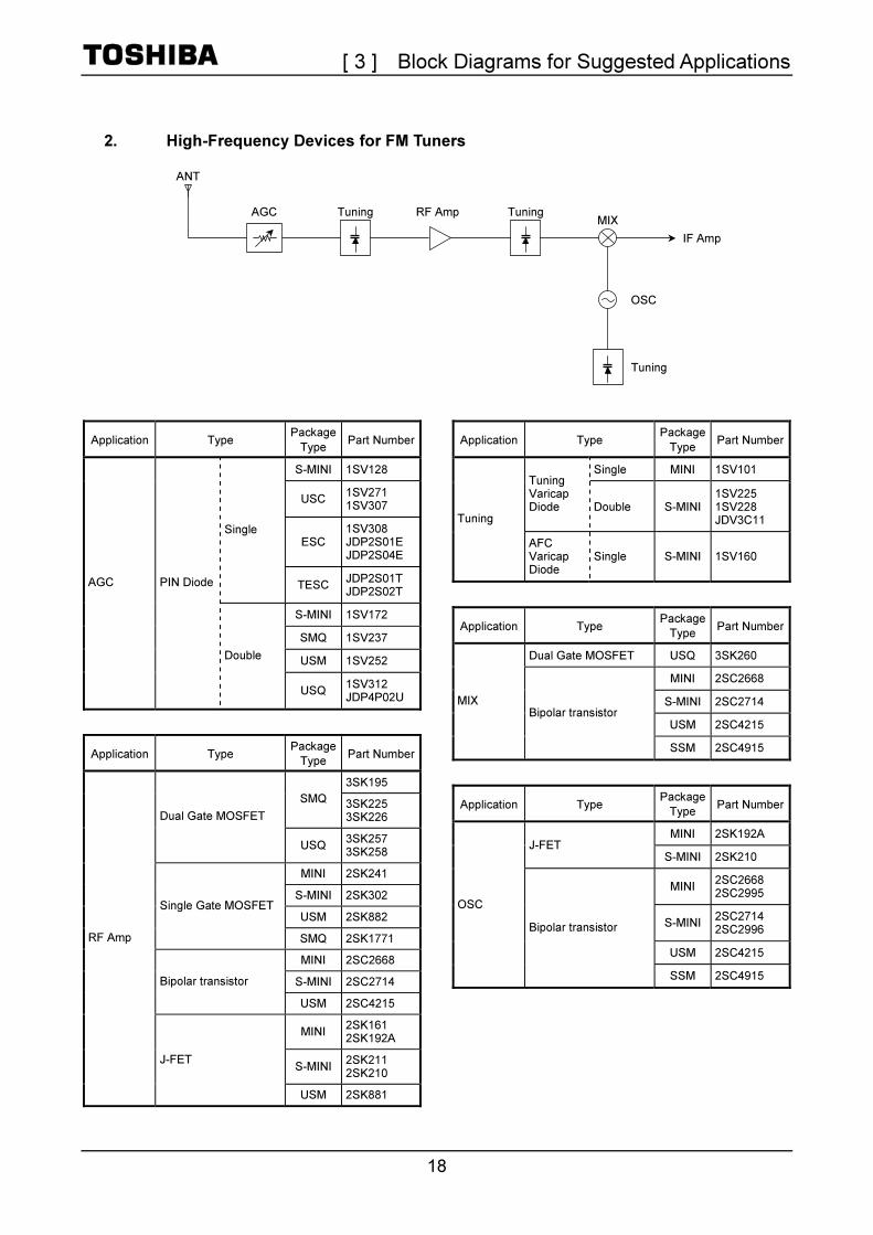
2. High-Frequency Devices for FM Tuners
Application Type Package
Type Part Number
S-MINI 1SV128
USC 1SV271 1SV307
ESC 1SV308 JDP2S01E JDP2S04E
Single
TESC JDP2S01T JDP2S02T
S-MINI 1SV172
SMQ 1SV237
USM 1SV252
AGC PIN Diode
Double
USQ 1SV312 JDP4P02U
Application Type Package
Type Part Number
3SK195
SMQ 3SK225 3SK226 Dual Gate MOSFET
USQ 3SK257 3SK258
MINI 2SK241
S-MINI 2SK302
USM 2SK882 Single Gate MOSFET
SMQ 2SK1771
MINI 2SC2668
S-MINI 2SC2714 Bipolar transistor
USM 2SC4215
MINI 2SK161 2SK192A
S-MINI 2SK211 2SK210
RF Amp
J-FET
USM 2SK881
Application Type Package
Type Part Number
Single MINI 1SV101 Tuning Varicap Diode Double S-MINI
1SV225 1SV228 JDV3C11 Tuning
AFC Varicap Diode
Single S-MINI 1SV160
Application Type Package
Type Part Number
Dual Gate MOSFET USQ 3SK260
MINI 2SC2668
S-MINI 2SC2714
USM 2SC4215
MIX Bipolar transistor
SSM 2SC4915
Application Type Package
Type Part Number
MINI 2SK192A J-FET
S-MINI 2SK210
MINI 2SC2668 2SC2995
S-MINI 2SC2714 2SC2996
USM 2SC4215
OSC
Bipolar transistor
SSM 2SC4915
Tuning RF Amp Tuning
Tuning
MIX
IF Amp
OSC
AGC
ANT
[ 3 ] Block Diagrams for Suggested Applications
19
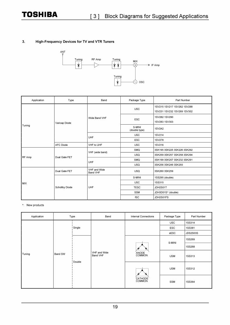
3. High-Frequency Devices for TV and VTR Tuners
Application Type Band Package Type Part Number
USC 1SV215 1SV217 1SV262 1SV288
1SV231 1SV232 1SV269 1SV302
ESC 1SV282 1SV290
1SV283 1SV303
Wide Band VHF
S-MINI (double type)
1SV242
USC 1SV214
Varicap Diode
UHF ESC 1SV278
Tuning
AFC Diode VHF to UHF USC 1SV216
SMQ 3SK195 3SK225 3SK226 3SK292 VHF (wide band)
USQ 3SK259 3SK257 3SK258 3SK294
SMQ 3SK199 3SK207 3SK232 3SK291 RF Amp Dual Gate FET
UHF USQ 3SK256 3SK249 3SK293
Dual Gate FET VHF and Wide Band VHF
USQ 3SK260 3SK259
S-MINI 1SS295 (double)
USC 1SS315
TESC JDH2S01T
SSM JDH3D01S* (double)
MIX
Schottky Diode UHF
fSC JDH2S01FS
*: New products
Application Type Band Internal Connections Package Type Part Number
USC 1SS314
ESC 1SS381 Single
sESC JDS2S03S
1SS269
S-MINI
1SS268
USM 1SS313
USM 1SS312
Tuning Band SW
Double
VHF and Wide Band VHF
SSM 1SS364
ANT
Tuning RF Amp TuningMIX
IF Amp
OSC
Tuning
ANODECOMMON
CATHODECOMMON
[ 3 ] Block Diagrams for Suggested Applications
20
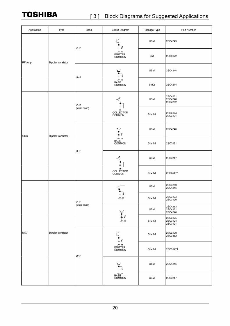
Application Type Band Circuit Diagram Package Type Part Number
USM 2SC4249
VHF
SM 2SC3122
USM 2SC4244
RF Amp Bipolar transistor
UHF
SMQ 2SC4214
USM 2SC4251 2SC4246 2SC4252
VHF (wide band)
S-MINI 2SC3124 2SC3121
USM 2SC4246
S-MINI 2SC3121
USM 2SC4247
OSC Bipolar transistor
UHF
S-MINI 2SC3547A
USM 2SC4250 2SC4245
S-MINI 2SC3123 2SC3120
USM 2SC4253 2SC4251 2SC4246
VHF (wide band)
S-MINI 2SC3125 2SC3124 2SC3121
S-MINI 2SC3120 2SC3862
S-MINI 2SC3547A
USM 2SC4245
MIX Bipolar transistor
UHF
USM 2SC4247
BASECOMMON
EMITTERCOMMON
EMITTERCOMMON
BASECOMMON
COLLECTORCOMMON
BASECOMMON
COLLECTORCOMMON
[ 3 ] Block Diagrams for Suggested Applications
21
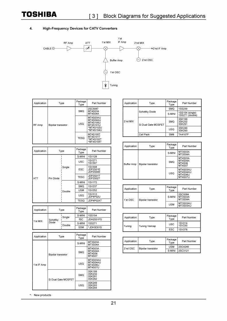
4. High-Frequency Devices for CATV Converters
Application Type Package
Type Part Number
SMQ 2SC5087 MT4S03A MT4S04A
USQ
MT4S03AU MT4S04AU MT4S100U MT4S101U *MT4S102U *MT4S104U
RF Amp Bipolar transistor
TESQ
MT4S100T MT4S101T *MT4S102T *MT4S104T
Application Type Package
Type Part Number
S-MINI 1SV128
USC 1SV271 1SV307
ESC 1SV308 JDP2S01E JDP2S04E
Single
TESC JDP2S01T JDP2S02T
S-MINI 1SV172
SMQ 1SV237
USM 1SV252
USQ 1SV312 JDP4P02U
ATT Pin Diode
Double
TESQ JDP4P02AT
Application Type Package
Type Part Number
S-MINI 1SS154 Single
fSC JDH2S01FS
S-MINI 1SS271 1’st MIX
Schottky Diode
Double SSM *JDH3D01S
Application Type Package
Type Part Number
S-MINI MT3S03A MT3S04A
SMQ
MT4S03A MT4S04A MT4S06 MT4S07
Bipolar transistor
USQ
MT4S03AU MT4S04AU MT4S06U MT4S07U
SMQ
3SK199 3SK232 3SK291 3SK292
1’st IF Amp
Si Dual Gate MOSFET
USQ 3SK249 3SK293 3SK294
*: New products
Application Type Package
Type Part Number
SMQ 1SS239 Schottky Diode
S-MINI 1SS154 (single) 1SS271 (double)
SMQ 3SK199 3SK232 3SK291 Si Dual Gate MOSFET
USQ 3SK249 3SK293
2’nd MIX
Cell Pack SM8 TA4107F
Application Type Package
Type Part Number
S-MINI MT3S03A MT3S04A
SMQ
MT4S03A MT4S04A MT4S06 MT4S07
Buffer Amp Bipolar transistor
USQ
MT4S03AU MT4S04AU MT4S06U MT4S07U
Application Type Package
Type Part Number
S-MINI 2SC5084 MT3S03A MT3S04A 1’st OSC Bipolar transistor
USM MT3S03AU MT3S03AU
Application Type Package
Type Part Number
USC 1SV214 1SV230 Tuning Tuning Varicap
ESC 1SV278
Application Type Package
Type Part Number
USM 2SC4246 2’nd OSC Bipolar transistor
S-MINI 2SC3121
ATT
Buffer Amp
CABLE
RF Amp 1’st MIX
1’st OSC
Tuning
2’nd MIX
2’nd IF Amp
2’nd OSC
1’st
IF Amp

[ 3 ] Block Diagrams for Suggested Applications
22
5. High-Frequency Devices for SHF 2nd Converters
Application Type Package
Type Part Number
SMQ
MT4S03A MT4S04A MT4S06 MT4S07 2SC5092
USQ
2SC5088 2SC5093 2SC5319 MT4S06U MT4S07U MT4S100U MT4S101U *MT4S102U*MT4S104U
1’st IF Amp Bipolar transistor
TESQ
MT4S100T MT4S101T *MT4S102T*MT4S104T
Application Type Package
Type Part Number
USC 1SV245 1SV287
Tuning Preselector and Tuning Varicap Diode
ESC 1SV309 1SV291
Application Type Package
Type Part Number
Bipolar transistor SMQ 2SC5087 2SC5092
S-MINI
1SS154 (single) 1SS271 (double)
SSM *JDH3D01S (Duble)
Schottky Diode
fSC JDH2S01FS
MIX
Cell Pack SM8 *TA4107F
Application Type Package
Type Part Number
SMQ 2SC5092 Bipolar transistor
S-MINI 2SC5089
SMQ TA4002F
2’nd IF Amp (1)
Cell Pack SMV TA4003F
Application Type Package
Type Part Number
SM6 TA4000F
TU6 TA4017FT
SM8 TA4018F
2’nd IF Amp (2)
Cell Pack
SM8 TA4019F
Application Type Package
Type Part Number
SMQ 2SC5092
Buffer Amp Bipolar transistor USQ
2SC5088 2SC5093 2SC5319
Application Type Package
Type Part Number
OSC Bipolar transistor S-MINI 2SC5089
*: New products
Package type: SMV (SSOP5-P-0.95)
Application Type Package Type Part
Number
2’nd converter IC Cell pack SSOP20-P-225 TA4303F
Tuning
Tuning
OSC
1’st IF Amp MIX 2’nd IF Amp (1)
Buffer Amp
2’nd IF Amp (2)
SAW Filter

[ 3 ] Block Diagrams for Suggested Applications
23
6. High-Frequency Devices for 800 MHz Band Analog and Digital Cellular Phones
Application Type Package
Type Part Number
Power Amp (JAPAN CDMA)
Module 5-6B S-AU84
Power Amp (US CDMA)
Module 5-6B S-AU85
Application Type Package
Type Part Number
2SK2854 Power Amp Si MOSFET PW-MINI
2SK2855
Application Type Package
Type Part Number
TG2210FT GaAs Cell Pack TU6
TG2211FT
USC ISS314
ESC ISS381
JDP2S02AFSfSC
*JDP2S05FS
Rx SW
PIN Diode
sESC JDS2S03S
Application Type Package
Type Part Number
TA4003F SMV
TA4004F
TA4011AFE Buff Amp Si Cell Pack
ESV TA4012AFE
Package
Type
Application Type
USC TESC
Detector SBD 1SS315 JDH2S01T
Package Type
Application
TESM fSM SMQ USQ
LNA, Buff Amp
2SC5066FT 2SC5086FT 2SC5091FT 2SC5096FT MT3S03AT MT3S06T MT3S07T MT3S14T MT3S17T MT3S18T MT3S35T MT3S36T MT3S37T MT3S38T MT3S40T MT3S41T
MT3S03AFS MT3S06FS MT3S07FS *MT3S14FS *MT3S17FS *MT3S18FS MT3S35FS MT3S36FS MT3S37FS MT3S38FS MT3S40FS MT3S41FS
2SC5087 2SC5092 2SC5097 MT4S06 MT4S07
2SC5088 2SC5093 2SC5098 MT4S06U MT4S07U MT4S32U
MIX
2SC5066FT 2SC5086FT 2SC5108FT 2SC5111FT
⎯
2SC5087
2SC5088
VCO
2SC5086FT 2SC5464FT 2SC5066FT 2SC5108FT 2SC5111FT MT3S03AT MT3S04AT MT3S05T MT3S06T MT3S07T MT3S08T MT3S11T MT3S12T MT3S14T *MT3S18T MT3S35T MT3S36T MT3S37T MT3S38T MT3S40T MT3S41T MT3S45T
MT3S03AFS MT3S04AFS MT3S05FS MT3S06FS MT3S07FS MT3S08FS *MT3S11FS *MT3S12FS *MT3S14FS *MT3S18FS MT3S35FS MT3S36FS MT3S37FS MT3S38FS MT3S40FS MT3S41FS MT3S45FS
⎯ ⎯
*: New products
Varicap Diode
Package Type
Application
USC ESC sESC fSC
VCO
1SV229 1SV270 1SV276 1SV304 1SV310
1SV279 1SV281 1SV284 1SV305 1SV311
JDV2S06S JDV2S08S JDV2S09S
JDV2S06FSJDV2S08FSJDV2S09FS
*: New products
Rx ANT Down Converter MIXLNA
Buff Amp
Driver Amp
Up Converter MIX
BPF
1st VCO
Power Amp
High Power SW or Duplexer
BPF
Rx SW
TRx ANT
BPF BPF
PLL
2nd VCO
Buff Amp

[ 3 ] Block Diagrams for Suggested Applications
24
7. High-Frequency Devices for PDC (1.5 GHz)
Package
Type
Application Type
TESM fSM USQ TESQ
LNA, Buff Amp
Bipolar transistor
2SC5317FT 2SC5322FT MT3S06T MT3S07T MT3S14T MT3S17T MT3S18T MT3S35T MT3S36T MT3S37T MT3S38T MT3S40T MT3S41T MT3S45T
MT3S06FS MT3S07FS *MT3S14FS *MT3S17FS *MT3S18FS MT3S35FS MT3S36FS MT3S37FS MT3S38FS MT3S40FS MT3S41FS MT3S45FS
2SC5319 MT4S06U MT4S07U MT4S100U MT4S101U
MT4S100T MT4S101T
Mixer (down)
Bipolar transistor
2SC5317FT 2SC5322FT 2SC5086FT
VCO Bipolar transistor
MT3S03AT MT3S04AT MT3S05T MT3S06T MT3S07T MT3S08T MT3S11T MT3S12T MT3S14T *MT3S18T MT3S35T MT3S36T MT3S37T MT3S38T MT3S40T MT3S41T MT3S45T
MT3S03AFS MT3S04AFS MT3S05FS MT3S06FS MT3S07FS MT3S08FS *MT3S11FS *MT3S12FS *MT3S14FS *MT3S18FS MT3S35FS MT3S36FS MT3S37FS MT3S38FS MT3S40FS MT3S41FS MT3S45FS
*: New products
Package Type
Application Type ESC sESC fSC
VCO VCD
JDV2S05E 1SV285 1SV305 1SV311 1SV314 1SV329
JDV2S05S JDV2S07S JDV2S08S JDV2S09S JDV2S10S JDV2S13S
JDV2S05FS JDV2S07FS JDV2S08FS JDV2S09FS JDV2S10FS JDV2S13FS
Package Type
Application Type ESV
Buff Amp Si Cell pack TA4011AFE TA4012AFE
Package Type
Application Type TU6
RF Switch GaAs Cell pack TG2211FT
Package Type
Application Type USC TESC fSC SSM
Detector SBD 1SS315 JDH2S01T JDH2S01FS *JDH3D01S
*: New products
1.5 GHz MixerLNA
Buffer Amp
RX
Switch
BPF
Pre Driver
BPF SawFilter
Mixer IF Amp
RSSI
P/S
PLL
P/S
PLL
VCO
BPFPower Amp
VCO
SBD
TX LPF
90DEG
LPF
LPF

[ 3 ] Block Diagrams for Suggested Applications
25
8. High-Frequency Devices for 900 MHz, 2.4 GHz and 5.8 GHz Band Cordless Phone
Packag
e Type
Applicatio
n
Frequency
Band
USC ESC sESC fSC CST2 USM SSM TESM SMQ USQ TESQ
900 MHz
1SV271 1SV307 1SS314
JDP2S04E1SV308 1SS381
JDP2S02AS JDS2S03S
JDP2S02AFS
*JDP2S02ACT
2.4 GHz
1SV271 1SV307
JDP2S04E1SV308
JDP2S02AS
JDP2S02AFS*JDP2S05FS
**JDP2S05CT
ANT Switch
5.8 GHz
*JDP2S05FS **JDP2S05CT
900 MHz
1SV214 1SV229 1SV276 1SV304 1SV310 1SV313
1SV278 1SV279 1SV284 1SV305 1SV311 1SV314
JDV2S06S JDV2S08S JDV2S09S
JDV2S06FSJDV2S08FSJDV2S09FS
2.4 GHz
JDV2S01EJDV2S02EJDV2S05E
JDV2S01S JDV2S02S JDV2S05S JDV2S16S JDV2S19S JDV2S20S
JDV2S01FSJDV2S02FSJDV2S05FSJDV2S16FSJDV2S19FSJDV2S20FS
VCO
5.8 GHz
JDV2S02E JDV2S02S *JDV2S17S JDV2S20S *JDV2S22S
JDV2S02FS*JDV2S17FSJDV2S20FS*JDV2S22FS
900 MHz
2SC5065 2SC5085 MT3S06U *MT3S16U
2SC50662SC5086MT3S06S
2SC5066FT 2SC5086FT MT3S06T *MT3S16T *MT3S17T *MT3S18T
2SC5087 MT4S06
2SC5088 MT4S06U
2.4 GHz
MT3S06U
2SC5317MT3S06S
2SC5317FT MT3S06T *MT3S17T *MT3S18T *MT3S35T
MT4S06
2SC5319 MT4S06U MT4S32U
VCO
Buffer Amp
Mixer
Power Amp
Pre Amp
LAN 5.8 GHz
MT3S35T MT3S37T
MT4S100UMT4S101U*MT4S102U*MT4S104U
MT4S100TMT4S101T*MT4S102T*MT4S104T
*: New products
**: Under development
LNA BPF
Buffer Amp
BPF
ANT Switch
Power AmpBPF Pre Amp
x2 VCO
Mixer

[ 3 ] Block Diagrams for Suggested Applications
26
9. High-Frequency Devices for GPS LNB
GPS Antenna Section
Package Type
Application Type
ES6 USQ TESQ
Bipolar transistor
2SC5319 MT4S32U *MT4S100U *MT4S101U *MT4S102U *MT4S104U
*MT4S100T *MT4S101T *MT4S102T *MT4S104T
Amp (2)
Si Cell-Pack *TA4016AFE
*: New products
Navigation Section
Package Type
Application Type
USQ TESQ
Amp (3) Bipolar transistor
2SC5319 MT4S06U MT4S32U *MT4S100U *MT4S101U *MT4S102U *MT4S104U
*MT4S100T *MT4S101T *MT4S102T *MT4S104T
Mixer, OSCBipolar transistor
2SC5319 MT4S06U
*: New products
Package Type
Application Type ESC sESC fSC
1SV314 JDV2S10S JDV2S10FS
1SV329 JDV2S13S JDV2S13FS
OSC Varicap Diode
JDV2S01E JDV2S02E JDV2S05E
JDV2S01S JDV2S02S JDV2S05S JDV2S16S *JDV2S17S JDV2S19S JDV2S20S *JDV2S22S
JDV2S01FS JDV2S02FS JDV2S05FS JDV2S16FS *JDV2S17FS JDV2S19FS JDV2S20FS *JDV2S22FS
*: New products
MIX
IF circuit
OSC
ANT
Amp (3)Amp (1) Amp (2)
GPS ANTENNA NAVIGATION SECTION

[ 3 ] Block Diagrams for Suggested Applications
27
10. 2.4 GHz Wireless LAN and Bluetooth
ANT-SW
Type Part Number
For Class 1 GaAs MMIC TG2216TU
GaAs MMIC TG2210FT
GaAs MMIC TG2211FT
GaAs MMIC TG2213S For Class 2, 3
GaAs MMIC TG2214S
Pin Diode JDP2S01AFS All Class
Pin Diode JDP2S02AFS
: Built-in inverter
Package
Type
Application Type
USQ TESQ
LNA Bipolar transistor
2SC5319 MT4S32U MT4S100U MT4S101U *MT4S102U *MT4S104U
MT4S100T MT4S101T *MT4S102T *MT4S104T
*: New products
Package
Type
Application Type
ESC sESC fSC
1SV314 JDV2S10S JDV2S10FS
1SV329 JDV2S13S JDV2S13FS
VCO Varicap Diode
JDV2S01E JDV2S02E JDV2S05E
JDV2S01S JDV2S02S JDV2S05S JDV2S16S JDV2S19S JDV2S20S
JDV2S01FSJDV2S02FSJDV2S05FSJDV2S16FSJDV2S19FSJDV2S20FS
Transceiver IC
ANT LNA
PA (Class1)
BPF
BPF
ANT-SW
Tank

[ 3 ] Block Diagrams for Suggested Applications
28
11. High-Frequency Devices for FRS, GMRS
Package
Application Type
USC ESC sESC fSC CST2 USM SSM TESM SMQ USQ
ANT Switch
1SS314 1SV271 1SV307
1SS381 JDP2S04E 1SV308
JDS2S03S JDP2S02AS
JDP2S02AFS*JDP2S05FS
*JDP2S02ACT
VCO
1SV214 1SV229 1SV276 1SV304
1SV278 1SV279 1SV284 1SV305 1SV282A
JDV2S06S JDV2S08S
JDV2S06FSJDV2S08FS
VCO
Driver Buffer
Amp
Mixer
LAN
FRS,
GMRS 2SC5065
2SC5085 MT3S06U *MT3S16U
2SC5066 2SC5086 MT3S06S
2SC5066FT 2SC5086FT MT3S06T *MT3S16T *MT3S17T *MT3S18T
2SC5087 MT4S06
2SC5088 MT4S06U
*: New products
Package
Application Type
PW-MINI PW-X
FRS 2SK3078A *2SK3656
Power Amp
GMRS 2SK3079A
*2SK3756
*: New products
LNA BPF
Buffer Amp
ANT Switch
Power Amp Driver Amp
VCO
Mixer Buffer Amp
Band Switch

[ 4 ] Maximum Ratings and Electrical Characteristics


[ 4 ] Maximum Ratings and Electrical Characteristics
31
[ 4 ] Maximum Ratings and Electrical Characteristics
1. Definition of Maximum Ratings
1.1 Maximum Ratings (for high-frequency bipolar transistors)
1) Collector-base voltage (VCBO)
Maximum permissible value of voltage between collector and base with emitter open at the
specified ambient temperature
2) Collector-emitter voltage (VCES)
Maximum permissible value of voltage between collector and emitter with base-emitter short
at the specified ambient temperature
3) Collector-emitter voltage (VCEO)
Maximum permissible value of voltage between collector and emitter with base open at the
specified ambient temperature
4) Emitter-base voltage (VEBO)
Maximum permissible value of voltage between emitter and base with collector open at the
specified ambient temperature
5) Collector current (IC)
Maximum permissible value of collector current at the specified ambient temperature.
Regardless of the states of base and emitter, a current exceeding the rated value cannot flow
through the collector.
6) Collector power dissipation (PC)
Maximum permissible power dissipation at the specified ambient temperature. Normally the
value is specified for room temperature. PC decreases with increase in ambient temperature. If a
device dissipates power in excess of the PC rating, it may be damaged electrically or thermally
due to the generation of heat. Note also that the specified PC value is the value for the device
alone. If the device is mounted on a PCB, its PC value will differ substantially.
7) Junction temperature (Tj)
Permissible junction temperature range for device operation. The device’s maximum power
consumption and operating temperature levels must be set so that the junction temperature
always remains within the Tj range.
8) Storage temperature range (Tstg)
Ambient temperature range within which the device must be stored while not being used.
Toshiba guarantees that the device will not be degraded if it is stored at a temperature within
the Tstg range.
[ 4 ] Maximum Ratings and Electrical Characteristics
32
1.2 Maximum Ratings (for MOSFETs)
1) Drain-source voltage (VDSS)
Maximum voltage that can be applied between drain and source when gate and source are
connected directly at the specified temperature
2) Gate-source voltage (VGSS)
Maximum voltage that can be applied between gate and source when drain and source are
connected directly at the specified temperature
3) Drain current (ID)
Maximum forward current that can flow in drain pin at the specified temperature
4) Reverse drain current (IDR)
Maximum reverse current that can flow in drain pin at the specified temperature
5) Power dissipation (PD)
Maximum power dissipation at the specified temperature
6) Channel temperature (Tch)
Maximum junction temperature during device operation
7) Storage temperature (Tstg)
Specified ambient temperature range for while MOSFET is not in use
1.3 Maximum Ratings (for MOS modules)
1) Power supply voltage (Vdd)
Maximum voltage that can be applied between Vdd pin and GND at the specified temperature
2) Control voltage (Vgg)
Maximum voltage that can be applied between Vgg pin and GND at the specified temperature
3) Current consumption (It)
Maximum current that can flow in all voltage pins at the specified temperature
4) Input power (Pi)
Maximum high-frequency power that can be applied to Pi pin at the specified temperature and
under the specified conditions
5) Output power (Po)
Maximum high-frequency power that can be measured at Po pin at the specified temperature
and under the specified conditions
6) Operating temperature (TC (opr))
Theoretical case temperature range for module operation. Toshiba guarantees that the module
will operate properly if the case temperature remains within this range while the module is
being used.
7) Storage temperature (Tstg)
Specified ambient temperature range for while module is not in use

[ 4 ] Maximum Ratings and Electrical Characteristics
33
1.4 Maximum Ratings (for bipolar modules)
1) Power supply voltage (VCC)
Maximum voltage that can be applied between VCC pin and GND at the specified temperature
2) Control voltage (Vcon)
Maximum voltage that can be applied between Vcon pin and GND at the specified temperature
3) Current dissipation (It)
Maximum current that can flow in all voltage pins at the specified temperature
4) Input power (Pi)
Maximum high-frequency power that can be applied to Pi pin at the specified temperature and
under the specified conditions
5) Output power (Po)
Maximum high-frequency power that can be measured at Po pin at the specified temperature
and under the specified conditions
6) Operating temperature (TC (opr))
Theoretical case temperature range for module operation. Toshiba guarantees that the module
will operate properly if the case temperature remains within this range while the module is
being used.
7) Storage temperature (Tstg)
Ambient temperature range within which the module must be stored while not being used
[ 4 ] Maximum Ratings and Electrical Characteristics
34
2. Definition of Electrical Characteristics
2.1 Electrical Characteristics (for high-frequency bipolar transistors)
Parameter Symbol Description
Collector-emitter breakdown voltage V (BR) CEO
Breakdown voltage between collector and emitter when the specified voltage is applied between collector and emitter with emitter common and base open
Collector-emitter breakdown voltage V (BR) CES
Breakdown voltage between collector and emitter when the specified collector current flows with emitter common, and base and emitter shorted.
Emitter-base breakdown voltage V (BR) EBO Breakdown voltage between emitter and base when the specified emitter current flows with base common and collector open.
DC current gain hFE
Ratio of collector current to base current when device is operating at the specified collector-emitter voltage and collector current and with emitter common
Output capacitance Cob Capacitance between collector and base at the specified collector-base voltage with base common
Input power Pi
High-frequency input power required to achieve the specified high-frequency output power under the specified operating conditions in the specified test circuit.
Output power Po
High-frequency output power when the specified high-frequency power is applied under the specified operating conditions in the specified test circuit.
[ 4 ] Maximum Ratings and Electrical Characteristics
35
2.2 Electrical Characteristics (for MOSFETs)
Parameter Symbol Description
Gate leakage current IGSS Gate current when the specified gate voltage is applied with source common, and drain and source shorted
Drain current, Drain cut-off current IDSS Drain current when the specified drain voltage is applied with gate and source shorted and source common
Source-drain breakdown voltage V (BR) DSS
Breakdown voltage between source and drain when the specified drain current flows with source common, and gate and source shorted.
Gate threshold voltage Vth Gate voltage when the specified drain current flows with source common, and the specified drain voltage applied.
Drain-source On resistance RDS (ON) Drain-source resistance when the specified drain current flows with source common, and the specified gate voltage applied.
Drain-source On voltage VDS (ON) Drain-source voltage when the specified drain current flows with source common, and the specified gate voltage applied.
Forward transfer admittance |YfS| Admittance obtained at ∆ID/∆VGS when the device is operating at
the specified frequency with source common and with the specified drain current and drain voltages applied
Input capacitance Ciss
Equivalent capacitance between gate and source when the device is operating at the specified frequency with source common, drain and source common and with the specified drain current and drain voltages applied
Output capacitance Coss
Equivalent capacitance between drain and source when the device is operating at the specified values of gate voltage, drain voltage and frequency, with source common, and gate and source shorted (AC shorted).
Reverse transter capacitance Crss
Equivalent capacitance between gate and drain when the device is operating at the specified frequency with source common and with the specified drain current and drain voltages applied
Output power Po
High-frequency output power when the specified high-frequency power is applied under the specified operating conditions in the specified test circuit.
Drain efficiency ηD
Ratio, expressed in percentage, between high-frequency output power and DC drain input power when the specified high-frequency power is applied under the specified operating conditions in the specified test circuit.
Power gain Gp
Power gain when the specified high-frequency power is applied under the specified operating conditions in the specified test circuit.

[ 4 ] Maximum Ratings and Electrical Characteristics
36
2.3 Electrical Characteristics (for modules)
Parameter Symbol Description
Frequency range fRANGE Frequency range for high-frequency device operation
Power output Po High-frequency power under the specified conditions
Power gain Gp High-frequency gain under the specified conditions
Overall efficiency ηt
Conversion efficiency of device under the specified conditions
ηt is defined as: ηt = Po × 100/Pi + Vcon × Icon + VCC × ICC.
Input VSWR VSWRin
Standing-wave ratio for input side of device under the specified conditions
VSWRin is defined as: VSWRin = 1 + ( Pi/Pr )/1 − ( Pi/Pr ).
Harmonics HRM Difference between fundamental harmonic and secondary frequency under the specified conditions
Load-resistance characteristics ⎯ Device will not be destroyed under the specified conditions.
Stability ⎯ Device will not oscillate abnormally under the specified conditions.

[ 5 ] Device Features in
Detail


[ 5 ] Device Features in Detail
39
[ 5 ] Device Features in Detail
1. High-Frequency Transistor Parameter
The main design parameters of a transistor include the device parameters which closely respond to
the internal operating mechanism of the transistor, and the circuit parameters which comprise a
matrix obtained by regarding the transistor as a terminal circuit network.
These latter-mentioned parameters are further divided into one group corresponding to
small-signal equivalent circuits (analog circuits), and another group describing large-signal
equivalent circuits (digital circuits); the demarcation between these two groups being made according
to the amplitude of signals to be handled by each.
Equivalent circuits have undergone very rapid development recently. Circuit designers pay close
attention to the application ranges and operating limits of the device being simulated in selecting an
appropriate equivalent circuit. Table 1.1 lists equivalent circuits presently employed in small-signal
applications.
The descriptions in this section will emphasize small-signal equivalent circuits they are used.
Table 1.1 List of Transistor Equivalent Circuits
Transistor
equivalent
circuits
Small-signal equivalent
circuits
(general linear circuits for
purposes such as
amplification, oscillation,
modulation, and
demodulation)
Large-signal equivalent circuits (nonlinear circuits
such as pulse, digital, and switching circuits)
Device parameters
Circuit parameters
Early’s T-type equivalent circuits
(common base circuits)
Giacoletto’s π-type equivalent circuits
(emitter and collector common circuits)
Matrices showing the relations among the inputs
and outputs by voltage and current
a, b matrices;
g, h matrices (low frequency);
y, z matrices (high frequency)
Matrices showing the relations among inputs and
outputs by power
s matrices (high frequency)
Current control model by Evers-Moll;
Current control model by Beaufoy-Sparkes;
Current control model by Linville;
other nonlinear models

[ 5 ] Device Features in Detail
40
1.1 Device Parameters
1.1.1 Early’s T-Type Equivalent Circuits
Figure 1.1 shows an Early’s T-type
equivalent circuit.
In this circuit,
re: Emitter resistance
Since this is a forward-biased resistance associated with the base-to-emitter junction,
represented by the following equation:
( )Ω=
Ee
qI
kTr ..............................................................................................(1)
where
k: Boltzman’s constant (1.38 × 10⁻²³ J/K)
T: Absolute temperature (K)
q: Electric charge of electron (1.60 × 10⁻¹⁹ C)
IE: Emitter current (A)
Equation (1) is changed as follows at normal temperature (300 K) if the emitter current is
represented by mA in:
( )( )Ω
Ι=
mA
26r
Ee ........................................................................................(2)
where Ce: Emitter capacitance (CTe + CDe)
The emitter capacitance is represented as a sum of the depletion layer capacitance and the
diffusion capacitance. Because the depletion layer capacitance in an emitter-to-base junction is
normally far smaller than the diffusion capacitance, it can in most cases be ignored. The
depletion layer capacitance CTe and the diffusion capacitance CDe are represented as:
( )FV
Nn2
AC
eb'0
qn
eeT −φ
ε
=
1
............................................................................(3)
where,
Ae: Emitter junction area (m2)
ε: permittivity
nN: Majority carrier density (m−3) on the side of higher specific resistance side
(NPN in this case)
φ0: Contact potential difference (potential fault ck. term when balanced) (V)
Vb’e: Potential applied to both ends of the base-to-emitter junction (1)
( )F2kTD
WqIC
2E
eD = .....................................................................................(4)
where,
W : Base width (m)
D : Diffusion coefficient of minority carrier in the base region (m2/s)
Figure 1.1 Early’s T-Type Equivalent Circuit
b’
b
rc
e
αie
Cc
c
Ce rbb’
ie
µVcb’
re + −
[ 5 ] Device Features in Detail
41
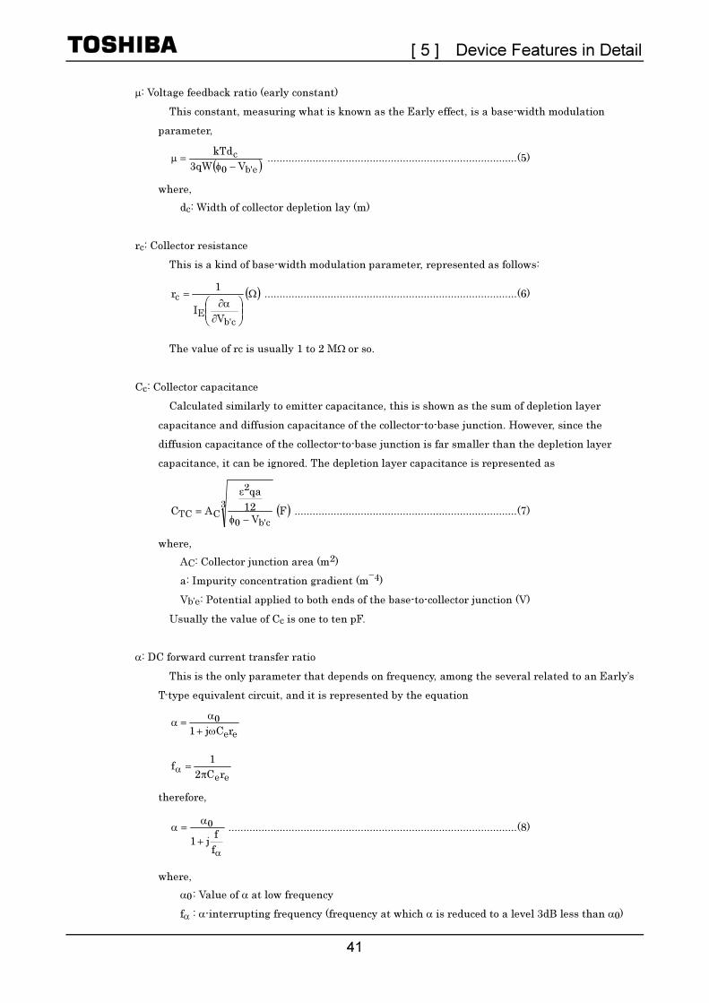
µ: Voltage feedback ratio (early constant)
This constant, measuring what is known as the Early effect, is a base-width modulation
parameter,
( )eb'0
c
V3qW
kTd
−φ=µ ...................................................................................(5)
where,
dc: Width of collector depletion lay (m)
rc: Collector resistance
This is a kind of base-width modulation parameter, represented as follows:
( )Ω
⎟⎟⎠
⎞⎜⎜⎝
⎛
∂
α∂=
cb'E
c
VI
1r ....................................................................................(6)
The value of rc is usually 1 to 2 MΩ or so.
Cc: Collector capacitance
Calculated similarly to emitter capacitance, this is shown as the sum of depletion layer
capacitance and diffusion capacitance of the collector-to-base junction. However, since the
diffusion capacitance of the collector-to-base junction is far smaller than the depletion layer
capacitance, it can be ignored. The depletion layer capacitance is represented as
( )FV
12
qa
AC3
cb'0
2
CTC −φ
ε
= ..........................................................................(7)
where,
AC: Collector junction area (m2)
a: Impurity concentration gradient (m−4)
Vb’e: Potential applied to both ends of the base-to-collector junction (V)
Usually the value of Cc is one to ten pF.
α: DC forward current transfer ratio
This is the only parameter that depends on frequency, among the several related to an Early’s
T-type equivalent circuit, and it is represented by the equation
ee
0
rCj1 ω+
α=α
eerC2
1f
π=
α
therefore,
α
+
α=α
f
fj1
0 ................................................................................................(8)
where,
α0 : Value of α at low frequency
fα : α-interrupting frequency (frequency at which α is reduced to a level 3dB less than α0)

[ 5 ] Device Features in Detail
42
Figure 1.2 shows the frequency locus of α. When actually measuring α, the difference between
theoretical and measured values increases as the frequency approaches fα. This is because the
Early’s equivalent circuit is based on an first approximation of physical phenomena.
To correct it, Thomas-Moll introduced excess phase m and offered the equation.
⎟⎟⎠
⎞⎜⎜⎝
⎛−
+
α=α
α
α
f
fjmexp
f
fj1
0 ..........................................................................(9)
Figure 1.2 Frequency Locus of α
The above equation agrees well with measured values in frequencies less than fα.
rbb’: Base diffusion resistance
This is resistance from the center of the base area to the external base terminal, which
actually contributes to transistor action. It is determined according to the shape and dimensions
of the transistor, and the base specific resistance.
rbb’ ∼ − ( )ΩπW8
qB .......................................................................................(10)
where,
qB: Specific resistance of base area (Ω・m)
DC Current gain (β) at the common emitter is represented as follows:
eb'eb'
0
eb'eb'0
0
rCj1rCj1
1
1 ω+
β=
ω+α−
α=β
The β-interrupting frequency fβ is defined as the frequency at which the absolute value of β
becomes 20β . fβ is represented similarly to fα, as:
eb'eb' rC2
1f
π
=β
therefore,
β
+
β=β
f
fj1
0 ...............................................................................................(11)
α
+
α=α
f
fj1
0
Re (α)
⎟⎟⎠
⎞⎜⎜⎝
⎛−
+
α=α
α
α
f
fjmexp
f
fj1
0
0.5
4
π
1.0
−j 0.5
Im (α) fα
m

[ 5 ] Device Features in Detail
43
1.1.2 Giacoletto’s π-Type Equivalent Circuit
Figure 1.3 shows the π-type equivalent circuit. This equivalent circuit is in itself the same as an
Early’s T-type equivalent circuit mentioned above. The only thing distinguishing the π-type circuit
from an Early’s T-type equivalent circuit is that in principle each parameter has no frequency
response.
Table 1.2 Relationship between
Parameters of the π-Type
and T-Type Equivalent
Circuits
π-Type Equivalent
Circuit Parameters
T-Type Equivalent
Circuit Parameters
Cb’e Ce
rbe’ 0
e
1
r
α−
Cb’c Cc
cb'r
1
( )
er
01
cr
1 α−µ−
rce µ
er
gm e
0
r
α
rbb’ rbb’
Parameters of the T-type equivalent circuit
and those of the π-type have the correlation
shown Table 1.2.
Figure 1.3 π-Type Equivalent Circuit
Because the physical meaning of each parameter is easy to understand, this circuit is popularly
employed. When actually employed for circuit calculation, it will prove convenient if the basic style
shown in Figure 1.3 is slightly simplified by restricting the frequency range to that which is
anticipated for performance of the device actually being simulated.
b
e
rbb’
rb’e
Cb’c
gm
c
rce
Vb’e
rb’c
b’
Cb’e
[ 5 ] Device Features in Detail
44
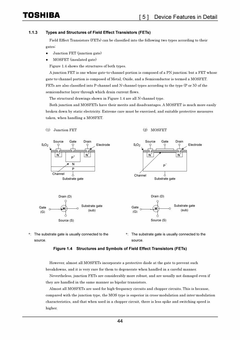
1.1.3 Types and Structures of Field Effect Transistors (FETs)
Field Effect Transistors (FETs) can be classified into the following two types according to their
gates:
Junction FET (junction gate)
MOSFET (insulated gate)
Figure 1.4 shows the structures of both types.
A junction FET is one whose gate-to-channel portion is composed of a PN junction; but a FET whose
gate-to-channel portion is composed of Metal, Oxide, and a Semiconductor is termed a MOSFET.
FETs are also classified into P-channel and N-channel types according to the type (P or N) of the
semiconductor layer through which drain current flows.
The structural drawings shown in Figure 1.4 are all N-channel type.
Both junction and MOSFETs have their merits and disadvantages. A MOSFET is much more easily
broken down by static electricity. Extreme care must be exercised, and suitable protective measures
taken, when handling a MOSFET.
(1) Junction FET (2) MOSFET
*: The substrate gate is usually connected to the
source.
*: The substrate gate is usually connected to the
source.
Figure 1.4 Structures and Symbols of Field Effect Transistors (FETs)
However, almost all MOSFETs incorporate a protective diode at the gate to prevent such
breakdowns, and it is very rare for them to degenerate when handled in a careful manner.
Nevertheless, junction FETs are considerably more robust, and are usually not damaged even if
they are handled in the same manner as bipolar transistors.
Almost all MOSFETs are used for high-frequency circuits and chopper circuits. This is because,
compared with the junction type, the MOS type is superior in cross-modulation and inter-modulation
characteristics, and that when used in a chopper circuit, there is less spike and switching speed is
higher.
Substrate gate
Source Gate Drain SiO2 Electrode
Channel
P+
N+
N
P
N+
Substrate gate
Source Gate Drain SiO2 Electrode
Channel
P−
N+
N+
Substrate gate
(sub)
Source (S)
Gate
(G)
Drain (D)
Substrate gate
(sub)
Source (S)
Gate
(G)
Drain (D)

[ 5 ] Device Features in Detail
45
When using FETs for a high-frequency circuit, it is necessary to reduce the internal feedback
capacitance to as low a level as possible, so that stable gain can be obtained. FETs with a cascode
connection are employed by adopting for this purpose.
In recent years, this problem has been solved in two different ways: by producing a cascode FET in
which two FETs are cascode-connected in the interior, as well as by development of dual-gate
MOSFETs.
Figure 1.5 illustrates the structure of a cascode FET, and a drawing of an equivalent connection for
it. A cascode FET has two junction gates, the one near the drain being connected to the substrate gate.
Thereby two FETs are produced, a common source FET and a common gate FET.
This structure causes feedback from the drain to be grounded as alternate current, producing a
FET with small reverse transfer capacitance.
Figure 1.5 Structure and Equivalent Connection Drawing of Cascode FET
Figure 1.6 shows the structure and equivalent connection drawings of a dual-gate MOSFET. As far
as the operating principle is concerned, this FET is identical with a cascode FET. In the dual-gate
MOSFET, gate 2 is lead out to be grounded for AC and to be supplied with positive bias voltage for DC,
when the FET is used in a high-frequency amplifier circuit. It is possible to use gate 2 as an injection
terminal when using the MOSFET in a mixing circuit.
Figure 1.6 Structure and Equivalent Connection Drawings of Dual-Gate MOSFET
The symbols used for a junction cascode FET and for a dual-gate MOSFET are illustrated in
Figure 1.7.
(1) Junction cascode FET (2) Dual-gate MOS FET
Figure 1.7 Symbols Used for Junction Cascode FET and Dual-Gate MOSFET
Other available FETs, in addition to those already described, include a power FET and a GaAs FET.
Source
(S)
Gate 1
(G1)
Drain
(D)
N+
P−
N+
Gate 2
(G2)
N+
Channel 1 Channel 2
Source
(S)
Gate 1
(G1)
Gate 2
(G2)
Drain
(D)
Gate
(G)
Source (S)
Drain (D)
Gate
(G)
Drain (D)
Source (S)
Gate 1
(G1)
Gate 2
(G2)
Source (S)
Drain (D)
Source
(S)
Gate
(G)
Drain
(D)
P+
N+
N
P
N+
P+
Drain
(D)
Gate
(G)
Source
(S)
[ 5 ] Device Features in Detail
46
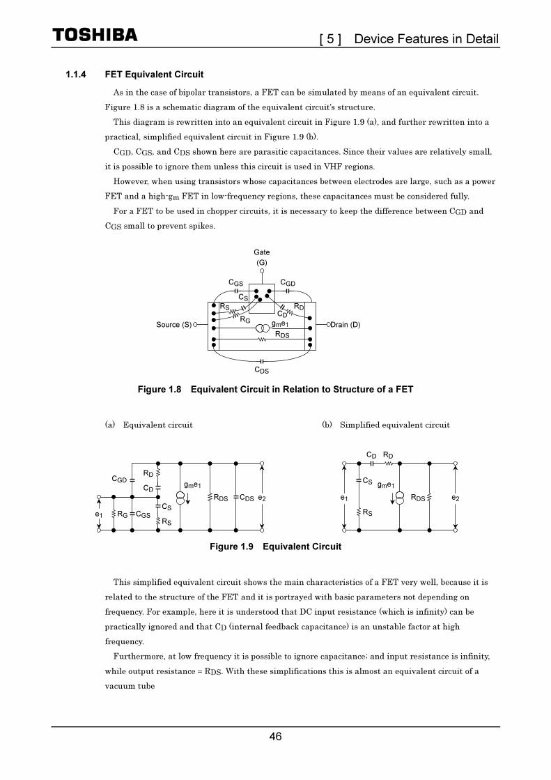
1.1.4 FET Equivalent Circuit
As in the case of bipolar transistors, a FET can be simulated by means of an equivalent circuit.
Figure 1.8 is a schematic diagram of the equivalent circuit’s structure.
This diagram is rewritten into an equivalent circuit in Figure 1.9 (a), and further rewritten into a
practical, simplified equivalent circuit in Figure 1.9 (b).
CGD, CGS, and CDS shown here are parasitic capacitances. Since their values are relatively small,
it is possible to ignore them unless this circuit is used in VHF regions.
However, when using transistors whose capacitances between electrodes are large, such as a power
FET and a high-gm FET in low-frequency regions, these capacitances must be considered fully.
For a FET to be used in chopper circuits, it is necessary to keep the difference between CGD and
CGS small to prevent spikes.
Figure 1.8 Equivalent Circuit in Relation to Structure of a FET
(a) Equivalent circuit (b) Simplified equivalent circuit
Figure 1.9 Equivalent Circuit
This simplified equivalent circuit shows the main characteristics of a FET very well, because it is
related to the structure of the FET and it is portrayed with basic parameters not depending on
frequency. For example, here it is understood that DC input resistance (which is infinity) can be
practically ignored and that CD (internal feedback capacitance) is an unstable factor at high
frequency.
Furthermore, at low frequency it is possible to ignore capacitance; and input resistance is infinity,
while output resistance = RDS. With these simplifications this is almost an equivalent circuit of a
vacuum tube
e1
CGD
RG CGS
RD
CD
CS
RS
gme1
RDS CDS e2 e1
CS
RS
gme1
CD RD
RDS e2
Drain (D) Source (S)
Gate
(G)
CGDCGS
RS
CS
RDS
RG
RDCD
gme1
CDS
[ 5 ] Device Features in Detail
47
1.2 Circuit Parameters
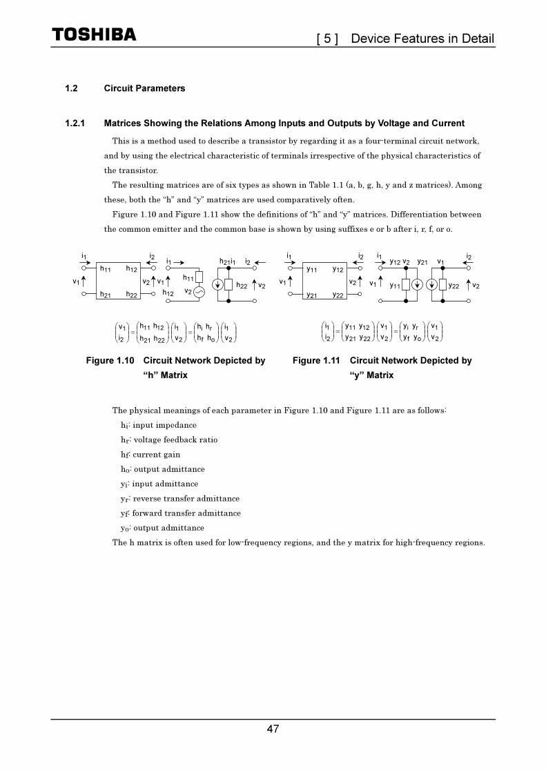
1.2.1 Matrices Showing the Relations Among Inputs and Outputs by Voltage and Current
This is a method used to describe a transistor by regarding it as a four-terminal circuit network,
and by using the electrical characteristic of terminals irrespective of the physical characteristics of
the transistor.
The resulting matrices are of six types as shown in Table 1.1 (a, b, g, h, y and z matrices). Among
these, both the “h” and “y” matrices are used comparatively often.
Figure 1.10 and Figure 1.11 show the definitions of “h” and “y” matrices. Differentiation between
the common emitter and the common base is shown by using suffixes e or b after i, r, f, or o.
⎟⎟⎠
⎞⎜⎜⎝
⎛⎟⎟⎠
⎞⎜⎜⎝
⎛=⎟
⎟⎠
⎞⎜⎜⎝
⎛
⎟⎟
⎠
⎞
⎜⎜
⎝
⎛=⎟
⎟⎠
⎞⎜⎜⎝
⎛
2
1
of
ri
2
1
2221
1211
2
1
v
i
h h
h h
v
i
h h
h h
i
v ⎟
⎟⎠
⎞⎜⎜⎝
⎛⎟⎟⎠
⎞⎜⎜⎝
⎛=⎟
⎟⎠
⎞⎜⎜⎝
⎛⎟⎟⎠
⎞⎜⎜⎝
⎛=⎟
⎟⎠
⎞⎜⎜⎝
⎛
2
1
of
ri
2
1
2221
1211
2
1
v
v
yy
yy
v
v
y y
yy
i
i
Figure 1.10 Circuit Network Depicted by
“h” Matrix
Figure 1.11 Circuit Network Depicted by
“y” Matrix
The physical meanings of each parameter in Figure 1.10 and Figure 1.11 are as follows:
hi: input impedance
hr: voltage feedback ratio
hf: current gain
ho: output admittance
yi: input admittance
yr: reverse transfer admittance
yf: forward transfer admittance
yo: output admittance
The h matrix is often used for low-frequency regions, and the y matrix for high-frequency regions.
v1
i1
v1
h12 v2
h21i1 i2
v2 h22
h11
i1 i2
v2
h11
h21
h12
h22
i1
v1
v2
y11
i1
v1
i2
v2
y11
y21
y12
y22
v2
i2
y22
v1 y21 y12

[ 5 ] Device Features in Detail
48
1.2.2 Matrix Showing the Relations Among Inputs and Outputs by Power
Such phenomena as the reflection and transfer of waves in a microwave circuit (for example, in
waveguides and cavity resonators) are usually indicated by an “S” matrix (scattering matrix).
As the frequency limits for semiconductor products expand, the “S” matrix itself is occasionally used
as a circuit parameter.
The definition of the “S” matrix is shown in Figure 1.12; the physical meanings of each parameter
are as follows:
S11: input reflection coefficient
S12: reverse transfer coefficient
S21: forward transfer coefficient
S22: output reflection coefficient
Suffix b or e is used to indicate the common base or the
common emitter in the same manner as y parameters and h
parameters.
⎟⎟⎠
⎞⎜⎜⎝
⎛⎟⎟⎠
⎞⎜⎜⎝
⎛=⎟
⎟⎠
⎞⎜⎜⎝
⎛⎟⎟⎠
⎞⎜⎜⎝
⎛=⎟
⎟⎠
⎞⎜⎜⎝
⎛
2
1
of
ri
2
1
2221
1211
2
1
a
a
S S
S S
a
a
S S
S S
b
b
Figure 1.12 Circuit Network Depicted
by “S” Matrix
a1
a2
b2
S11
S21
S12
S22b1
1 2
1’ 2’

[ 5 ] Device Features in Detail
49
Table 1.3 Conversion of Parameters
[H] [Y] [S]
hi hr iy
1
i
r
y
y−
[H]
hf ho i
f
y
y
i
froi
y
yyyy −
( ) ( )( ) ( ) froi
froi
SSS1S1
SSS1S1
++−
−++
( ) ( ) froi
r
SSS1S1
2S
++−
( ) ( ) froi
f
SSS1S1
2S
++−
−
( ) ( )( ) ( ) fSrSoS1iS1
fSrSiS1oS1
++−
−−−
ih
1
i
r
h
h− yi yr
[Y]
i
f
h
h
i
froi
h
hhhh − yf yo
( ) ( )( ) ( ) froi
frio
SSS1S1
SSS1S1
−++
+−+
( ) ( ) froi
r
SSS1S1
2S
−++
−
( ) ( ) froi
f
SSS1S1
2S
−++
−
( ) ( )( ) ( ) froi
fri
SSS1S1
SSSo1S1
−++
+−+
Si Sr
[S]
( ) ( )( ) ( ) froi
froi
hh1h1h
hh1h1h
−++
−+−
( ) ( ) froi
r
hh1h1h
2h
−++
( ) ( ) froi
f
hh1h1h
2h
−++
−
( ) ( )( ) ( ) froi
froi
hh1h1h
hhh1h1
−++
+−+
( ) ( )( ) ( ) froi
froi
yyy1y1
yyy1y1
−++
++−
( ) ( ) froi
r
yyy1y1
2y
−++
−
( ) ( ) froi
f
yyy1y1
2y
−++
−
( ) ( )( ) ( ) froi
froi
yyy1y1
yyy1y1
−++
+−+
Sf So

[ 5 ] Device Features in Detail
50
Table 1.4 Conversion Formulas for “h” Parameters
Converted “h” Parameters
Common Base Common Emitter Common Collector
fb
ib
h1
h
+
fb
rbb
h1
hh
+
−∆
fb
ib
h1
h
+
1
Com
mon
Base
fb
fb
h1
h
+
−
fb
oh
h1
h
+
fbh1
1
+
−
fb
ob
h1
h
+
fe
ie
h1
h
+
fe
ree
h1
hh
+
−∆ hie 1 − hre
Com
mon
Em
itte
r
fe
fe
h1
h
+
−
fe
oe
h1
h
+
− (1 + hfe) hoe
fc
ic
h
h− 1
h
h
fc
c−
∆− hic 1 − hrc
Know
n “
h”
Para
mete
rs
Com
mon
Colle
cto
r
( )
fc
fc
h
h1+−
fc
oc
h
h − (1 + hfc) hoc
∆he = hie・hoe − hre・hfe, ∆hb = hib・hob − hrb・hfb, ∆hc = hic・hoc − hrc・hfe
Table 1.5 Conversion Formulas for “y” Parameters
Converted “y” Parameters
Common Base Common Emitter Common Collector
Com
mon
Base
∑yb
− (yfb + yob)
− (yrb + yob)
yob
∑yb
− (yib + yrb)
− (yib + yob)
yib
Com
mon
Em
itte
r
∑ye
− (yfe + yoe)
− (yre + yoe)
yoe
yie
− (yie + yfe)
− (yie + yre)
∑ye
Know
n “
y”
Para
mete
rs
Com
mon
Colle
cto
r
yoc
− (yrc + yoc)
− (yfc + yoc)
∑yc
yic
− (yic + yrc)
− (yic + yrc)
∑yc
∑ye = yie + yre + yfe + yoe
∑yb = yib + yrb + yfb + yob
∑yc = yic + yrc + yfc + yoc

[ 5 ] Device Features in Detail
51
Table 1.6 “h” Parameters Converted by Early’s T-Type Device Parameters
Common Base Common Emitter
hib ( )
( )α
α
+
⎟⎟⎠
⎞⎜⎜⎝
⎛+α−+
ffj1
f
fj1rr 0bb'e
hie ( ) ( )
α+α−
+
ffj1
rr
0
ebb'
hrb j2πfCcrbb’ hre
( ) ( )α
α
α
+α−π
ffj1
f
fj
rCf20
ec
hfb ( )α
+
α−
ffj1
0 hfe ( ) ( )α
+α−
α
ffj1 0
0
hob j2πfCc hoe
( ) ( )α
αα
α
+α−
⎟⎟⎠
⎞⎜⎜⎝
⎛+
πffj1
f
fj1
f
fj
Cf20
c
Table 1.7 “y” Parameters Converted by Early’s T-Type Device Parameters
Common Base Common Emitter
yib
α
α
+
+
f
fjrr
f
fj1
bb'e
yie
( )
α
α
+
+α−
f
fjrr
f
fj1
bb'e
0
yrb
α
αα
α
+
⎟⎟⎠
⎞⎜⎜⎝
⎛+
π−
f
fj
r
r
f
fj1
f
fj
Cf2
bb'
ec yre
α
α
α
+
π−
f
fj
r
r
f
fj
r
rCf2
bb'
ebb'
ec
yfb
α
+
α−
f
fjrr bb'e
0 yfe
α
+
α
f
fjrr bb'e
0
yob
α
αα
α
+
⎟⎟⎠
⎞⎜⎜⎝
⎛++
π
f
fj
r
r
f
fj
r
r1
f
fj
Cf2
bb'
e
bb'
e
c yoe
α
αα
α
+
⎟⎟⎠
⎞⎜⎜⎝
⎛++
π
f
fj
r
r
f
fj
r
r1
f
fj
Cf2
bb'
e
bb'
e
c
Note: The common base parameter yob and the common emitter parameter yoe are identical.

[ 5 ] Device Features in Detail
52
(1) Common base (1) Common base
(a) (b) (a) (b)
(c) (d) (c) (d)
(2) Common emitter (2) Common emitter
(a) (b)
(c) (d)
Figure 1.13 Frequency Locus of “h”
Parameters
Figure 1.14 Frequency Locus of “y”
Parameters
Please refer to Table 1.3, Table 1.4, and Table 1.5 for the correlation and conversion among circuit
parameters of common base and common emitter. Figure 1.13, and Figure 1.14 show the frequency
locuses of “h” and “y” parameters obtained from Table 1.6, and Table 1.7.
The above-mentioned parameters vary according to the operating points and temperature, and
circuit designers must allow for such variations.
Re (hib) →
I m (
hib
) →
f fα
re rbb’ 0
I m (
yrb
) →
fα f
0−2πfαCc
Im (yrb) →
I m (
hfb
) →
0
fα
f
−α0
Re (hfb) →
0 Re (hob) →
f
→ I m
(hob)
→
Re (hre) →
I m (
hre
) →
0 2πfαCcre
fβ
f
bb'
ecr
rCf2
απ−
fβ
f
I m (
yre
) →
0
Re (yre) →
I m (
hoe)
→
2πfαCc Re (hoe) →
0
fβ
f
Solid line: theoretical curves
Hyphenated line: measured
I m (
hrb
)
→
f
→
Re (hrb) →0
0
ebb'
1
rr
α−
+
I m (
hie
) →
0
fβ
Re (hie) →
f
rbb’
e
0
r
α−
fα
I m (
yfb
) →
Re (yfb) →0
f fα
f
0
Re (yob) →
2πfαCc (1 + re/rbb’)
I m (
yob)
→
e
0
r
1 α−
bb'r
1
I m (
yie
) →
fαf
fβ
Im (yie) →
I m (
yib
) →
f fα
Re (yib) →bb'r
1
er
1
Re (yfe) →
I m (
yfe
) →
fβ
f
e
0
r
α
Re (hfe) →
0
I m (
hfe
) →
fβ
fβ f
0
0
1 α−
α
[ 5 ] Device Features in Detail
53
2. Gain and Stability
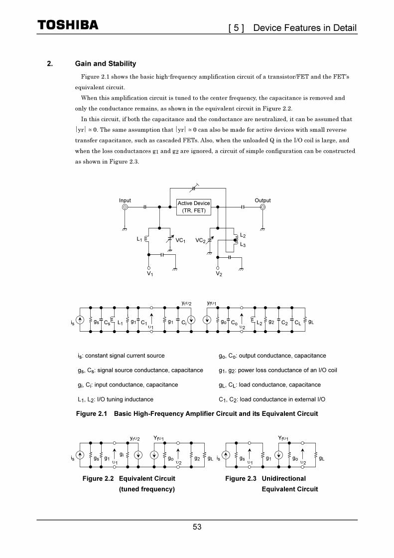
Figure 2.1 shows the basic high-frequency amplification circuit of a transistor/FET and the FET’s
equivalent circuit.
When this amplification circuit is tuned to the center frequency, the capacitance is removed and
only the conductance remains, as shown in the equivalent circuit in Figure 2.2.
In this circuit, if both the capacitance and the conductance are neutralized, it can be assumed that
⎪yr⎪ ∼ − 0. The same assumption that ⎪yr⎪ ∼− 0 can also be made for active devices with small reverse
transfer capacitance, such as cascaded FETs. Also, when the unloaded Q in the I/O coil is large, and
when the loss conductances g1 and g2 are ignored, a circuit of simple configuration can be constructed
as shown in Figure 2.3.
is: constant signal current source go, Co: output conductance, capacitance
gs, Cs: signal source conductance, capacitance g1, g2: power loss conductance of an I/O coil
gi, Ci: input conductance, capacitance gL, CL: load conductance, capacitance
L1, L2: I/O tuning inductance C1, C2: load conductance in external I/O
Figure 2.1 Basic High-Frequency Amplifier Circuit and its Equivalent Circuit
Figure 2.2 Equivalent Circuit
(tuned frequency)
Figure 2.3 Unidirectional
Equivalent Circuit
gs gog1 is
yrυ2
υ1 υ2
gi
Yfυ1
g2 gL gsis g1υ1
go υ2
Yfυ1
gL
Active Device
(TR, FET)
VC1
OutputInput
VC2
V2V1
L1 L2
L3
gs CoL1 g1 C1 υ1
g1 Cigo
υ2L2 g2 C2 CL gL Cs is
yrυ2 yfυ1
[ 5 ] Device Features in Detail
54
We now find the power gain of the equivalent circuit.
s2
s
L2
2
i
op
/4gi
g
(max) P
PG
⎪⎪
⎪υ⎪== ............................................................................. (1)
Combining with
( )is1sLo
12 ggi ,
gg
yf+υ−=
+
υ=υ
we obtain
( ) ( )2Lo2
is
Ls2
fp
gggg
ggy 4G
++
⎪⎪= .............................................................................. (2)
When gs = gi, and gL = go the power gain becomes maximum; these conditions are met when the
input and the output are matched.
oi
2fs
pg4g
y (max)G
⎪⎪= ......................................................................................... (3)
Gp (max) is the Maximum Available Gain (MAG) that can be achieved when the circuit and device
impedance are matched at both the input and output interfaces, while input-to-output signal transfer
is unidirectional.
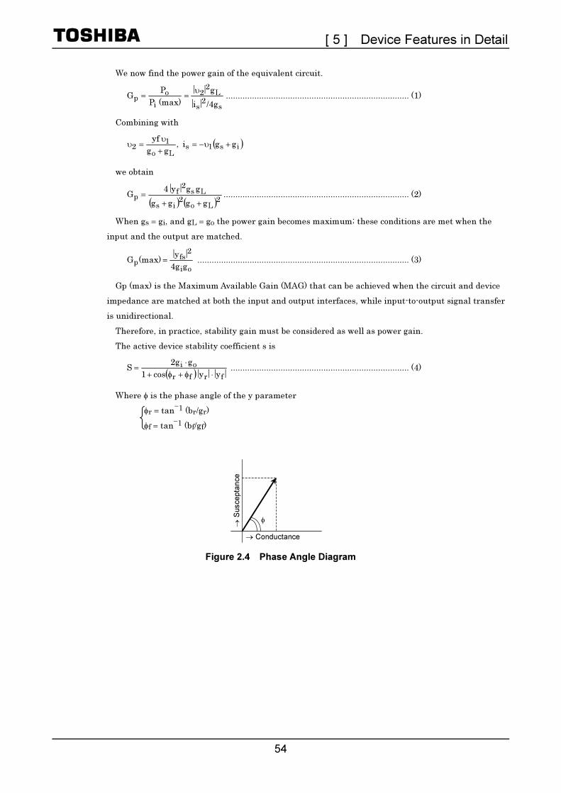
Therefore, in practice, stability gain must be considered as well as power gain.
The active device stability coefficient s is
( ) ⎪⎪⎪⋅⎪φ+φ+
⋅=
frfr
oi
y ycos1
g2g S ........................................................................... (4)
Where φ is the phase angle of the y parameter
φr = tan−1 (br/gr)
φf = tan−1 (bf/gf)
Figure 2.4 Phase Angle Diagram
→ Conductance
→ S
uscepta
nce
φ

[ 5 ] Device Features in Detail
55
The stability coefficient is calculated from the device’s y parameter, and, if s > 1, the device can be
deemed stable without considering the I/O circuit; however, when s <= 1, there is a danger that the I/O
circuit may cause oscillation.
In a high-frequency amplifier circuit, total stability S is expressed in terms of Gi and Go.
( ) ⎪⎪⎪⎪
⋅⋅
φ+φ+=
fr
oi
fr y y
GG
cos1
2 S .......................................................................... (5)
Where Gi = gs + g1 + gi
G0 = g0 + g2 + gL
The relationship between S and the stability coefficient of a device (s) can be expressed as follows
sgg
GG S
oi
oi ⋅=
sg
gg1
g
gg1
o
2L
1
1s ⋅⎟⎟⎠
⎞⎜⎜⎝
⎛ ++⎟
⎟⎠
⎞⎜⎜⎝
⎛ ++= .................................................................. (6)
S > = s
In other words, the circuit stability can be increased by selecting larger gs, gL, g1, or g2.
When the input and output are matched, even though the loss conductance of the coil is (g1, g2) = 0,
Gi = gs + gi = 2gi
Go = go + gL = 2go
S = 4 s
and total circuit stability four times greater than that of the device alone can be attained.
Power gain Gp can be expressed as a function of S:
( ) ⎪⎪
⎪⎪⋅
φ+φ+⋅=
f
f
frp
y
y
cos1
2
S
1 G ......................................................................... (7)
This formula can be changed to
( ) oi
2f
fr
oi
frp
g4g
y
y y
gg
cos1
2
S
4 G
⎪⎪⋅
⎪⎪⎪⎪
⋅⋅
φ+φ+⋅= ....................................................... (8)
(max)GS
4sp⋅= ........................................................................................ (9)
An S value of at least 4 (S > = 4) indicates good circuit stability.
Gp < = s・Gp (max).......................................................................................... (10)
If S < = 1, indicating poor device stability the MAG of the device is upper limit of the power gain
which can be attained in the circuit.
[ 5 ] Device Features in Detail
56
Table 2.1 shows the Gp of a high-frequency transistor/FET when MAG and S = 4.
Table 2.1 Gain and Stability (example)
f = 100 MHz
MAG (dB) s Gps (dB)
TR 2SC1923 34.9 0.030 19.6
2SK192A 26.9 0.023 10.5 J-FET
2SK161 26.4 0.265 20.7
MOS FET 2SK241 34.0 0.120 24.8
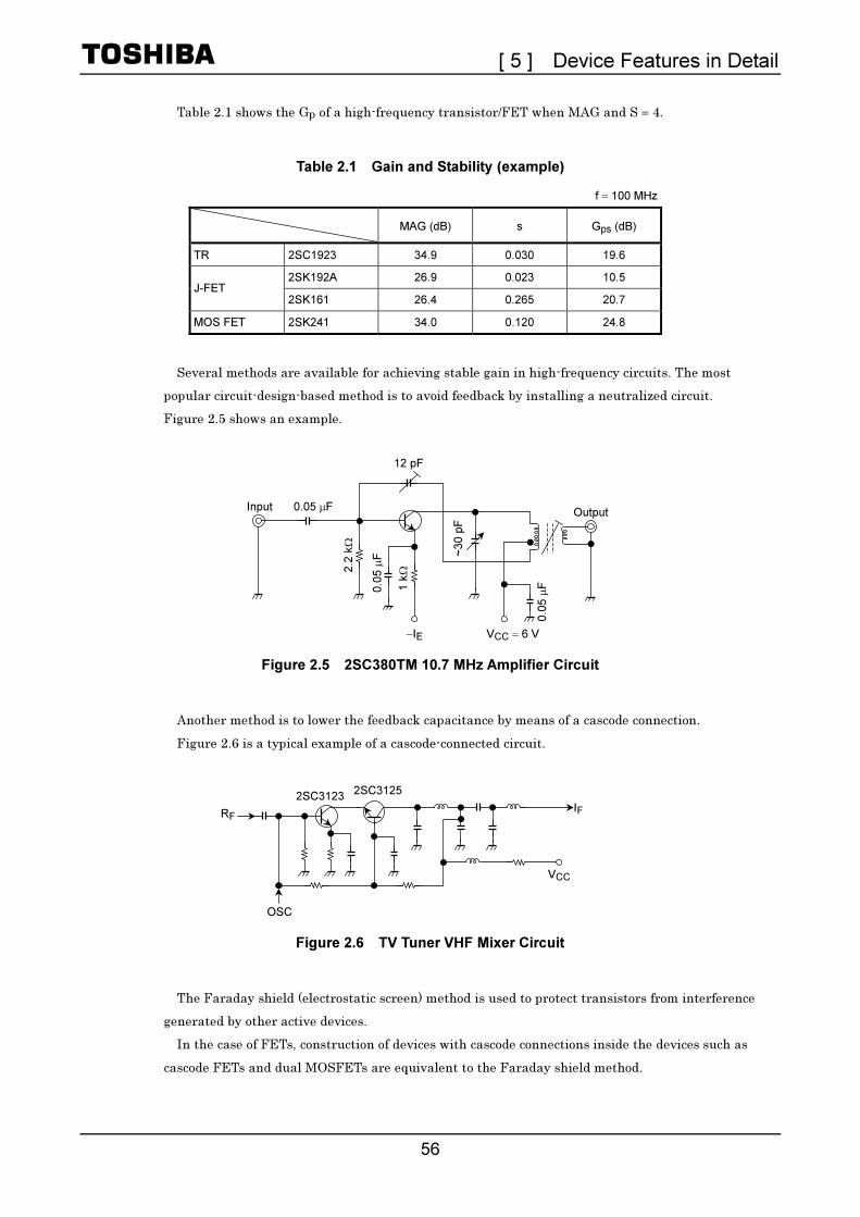
Several methods are available for achieving stable gain in high-frequency circuits. The most
popular circuit-design-based method is to avoid feedback by installing a neutralized circuit.
Figure 2.5 shows an example.
Figure 2.5 2SC380TM 10.7 MHz Amplifier Circuit
Another method is to lower the feedback capacitance by means of a cascode connection.
Figure 2.6 is a typical example of a cascode-connected circuit.
Figure 2.6 TV Tuner VHF Mixer Circuit
The Faraday shield (electrostatic screen) method is used to protect transistors from interference
generated by other active devices.
In the case of FETs, construction of devices with cascode connections inside the devices such as
cascode FETs and dual MOSFETs are equivalent to the Faraday shield method.
Input
2.2
kΩ
0.05 µF
0.0
5 µ
F
12 pF~
30 p
F
−IE
Output
1 kΩ
0.0
5 µ
F
VCC = 6 V
2SC3123
VCC
2SC3125
OSC
RF IF

[ 5 ] Device Features in Detail
57
3. Hight-Freguency 3-Pin MOSFET
This 3-pin MOSFET is a new device that leads current electronics technology.
Prior to introduction of this further innovation, the dual-gate MOSFET has been the most popular
type of conventional high-frequency MOSFET.
In this device, Gate 2 already had features offering several advantages when compared to
junction-type FETs or bipolar transistors.
Generally, Gate 2 can be used as the local oscillation signal injector terminal for mixer circuits, and
an AGC terminal.
However, there is an alternative application technique for dual-gate MOSFETs, as shown in
Figure 3.1. This shows a typical high-frequency amplifier in a Hi-Fi tuner. In the circuit depicted by
this figure, Gate 2 is used only as a DC fixed-bias terminal, in order to achieve power gain.
Figure 3.1 Figure 3.2
Assuming that a dual-gate MOSFET can achieve good performance when the Gate 2 bias voltage is
zero, Gate 2 only needs to be grounded; however, in practice, in this device Gate 2 has to be biased in
a voltage range of 3 to 5 V.
Passive components required for this purpose are at least two resistors and one capacitor.
However, a 3-terminal MOSFET does not require such components, yet can achieve the same
characteristics as a dual-gate MOSFET.
The 3-terminal MOSFET is a cascode-connected device, in which Gate 2 of the dual-gate MOSFET
is connected to the source.
In addition, special consideration has been given to maintaining excellent performance even when
Gate 2 is zero biased: this is achieved by using the channel control from the Gate 2 side.
Moreover, our original manufacturing technique allows reliability is improved by a decrease in the
amount of bonding.
Three types of packages are available, suitable for current compact FM tuners: Mini Mold (2SK241),
Super Mini (2SK302), and Ultra Super Mini (2SK882).
2 resistors and
1 condenser
can be saved.
VDD
Unnecessary
Dual-gate MOSFET
ANT
MIX
3-terminal MOSFET
ANT
MIX
VDD
Dual-gate MOSFET
G1
G2 S
D
3-terminal MOS FET
G
S
D
[ 5 ] Device Features in Detail
58
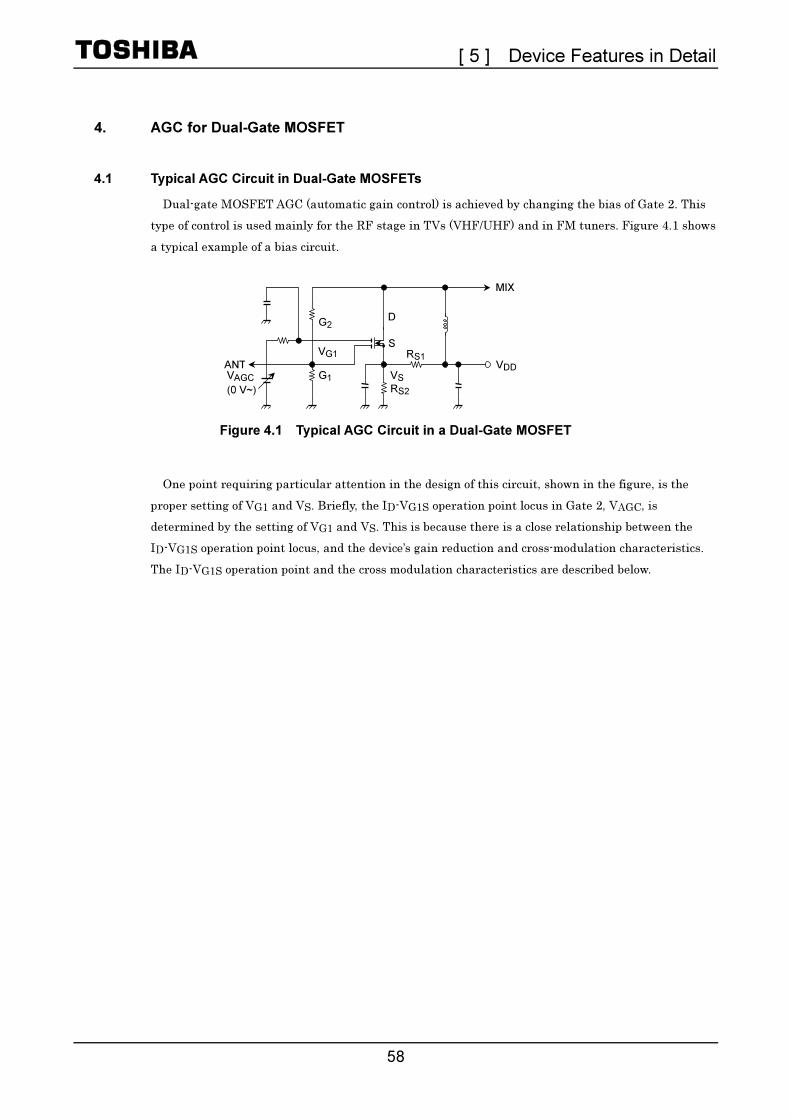
4. AGC for Dual-Gate MOSFET
4.1 Typical AGC Circuit in Dual-Gate MOSFETs
Dual-gate MOSFET AGC (automatic gain control) is achieved by changing the bias of Gate 2. This
type of control is used mainly for the RF stage in TVs (VHF/UHF) and in FM tuners. Figure 4.1 shows
a typical example of a bias circuit.
Figure 4.1 Typical AGC Circuit in a Dual-Gate MOSFET
One point requiring particular attention in the design of this circuit, shown in the figure, is the
proper setting of VG1 and VS. Briefly, the ID-VG1S operation point locus in Gate 2, VAGC, is
determined by the setting of VG1 and VS. This is because there is a close relationship between the
ID-VG1S operation point locus, and the device’s gain reduction and cross-modulation characteristics.
The ID-VG1S operation point and the cross modulation characteristics are described below.
VAGC
(0 V~)
MIX
RS1
RS2
VSG1
VG1
G2D
S
ANT VDD

[ 5 ] Device Features in Detail
59
4.2 Relationship Between VG1S and Cross Modulation, ⎪yfs⎪, ID
The characteristics shown as a representative example in Figure 4.2 relate both forward
conductance ⎪yfs⎪ and cross-modulation (undesired signal level) to the Gate 1-to-source voltage VG1S.
Three “good” points corresponding to peaks of the cross-modulation curve (D, E, F) of the 1% cross
modulation characteristic in the ⎪yfs⎪-versus-VG1S characteristics can be seen; and three “bad” points
corresponding to off-peak cross-modulation values (A, B, C) can also be seen.
Figure 4.2 ID, ⎪yfs⎪, X-Mod–VG1S Characteristics
In short, the figure shows that in a region with a sharp ⎪yfs⎪–VG1S curve, the second-order ⎪yfs⎪
(third-order ID) term is large, and therefore is bad; regions of the ⎪yfs⎪ curve which are nearly linear
are good since secondary ⎪yfs⎪ is small. Explanation of each point is as follows.
U
nde
sire
d s
ignal le
vel X
-Mo
d (d
Bµ
) 50 Ω
O
pe
n
VGIS (V) I D
(m
A),
⎪yfs⎪
(m
s)
0
80
70
100
90
110
1 2 3 4
20
10
ID
X-Mod
⎪yfs⎪A
B
C
D
E
F
[ 5 ] Device Features in Detail
60
4.2.1 Point A
This point is that in a dual-gate MOSFET, in the section close to the OFF state of the front-stage
FET, which is similar to that of a single-gate FET or to a bipolar transistor’s reverse AGC, the place
where GR (gain reduction) is large actually has very poor cross-modulation characteristics. Therefore,
in a dual-gate FET, it is strongly advisable not to allow Gate 1’s operation point, having a large GR, to
fall in the A range in which AGC is applied at Gate 2.
4.2.2 Point B
From the viewpoint of the ID–VG1S (or ⎪yfs⎪–VG1S) characteristic, this is the point where the
rear-stage FET starts to have an effect (the front-stage FET, however, is controlled by the A and F
points). This is a point that exists at all times if the device is a dual-gate FET. The VG1S at this point
is characterized by VG2S becoming smaller, as VG2S moves close to the VG1S (OFF) state, and the
cross-modulation tends to worsen. However, this point is passed through when the actual GR is small
(VG2S is large). Therefore, mounting the device on a tuner is not a problem since the cross-modulation
of the FET is buried by the cross modulation (of the mixer) which follows the RF amplifier stage.
4.2.3 Point C
From point B which is affected by the rear-stage FET, ID–VG1S characteristics is one step before
being more affected by the rear-stage FET. It’s like point B, this point exists if a device is the
dual-gate FET. The point’s position on VG1S. The cross-modulation shows bad same as point B.
However, this problem that is different form point B arises. If the cross-modulation is bad on this
point, that affects tuner characteristics to be bad because the GR (gain reduction) is passing through
GR = 10 to 30dB.
4.2.4 Point D, F
Between the “bad” points A and B with poor cross-modulation, and similarly between B and C,
there must exist two “good” points D and F. In other words, when ID is taken as a Taylor series
expansion of VG1S, the third-and first-order terms, exhibit counter-action changes in magnitude, and
being opposite in sign inevitably a point is eventually reached at which the sum of the third-and
first-order terms equals zero. These points of inflection are in principle very desirable as operating
points. However, in practice it is difficult to use them in design because they are difficult to locate
precisely.
4.2.5 Point E
With respect to ID–VG1S (or ⎪yfs⎪–VG1S) characteristics, this is a point strongly affected by the
rear-stage FET characteristics. One feature of this section is that GR is relatively large and cross
modulation is good (This is the most advantageous feature of a dual-gate FET). Note that for lower
VG2S values, the ⎪yfs⎪ curve becomes flatter and the ranges of VG1S corresponding to desirable
nearly-linear segments of the curve become wider gain reduction.
When applied AGC is to VG2S, the device must be designed to place its operating point at point E
which corresponds to VG1S values where gain reduction is high, in order to make best use of the
advantages of a dual-gate FET.
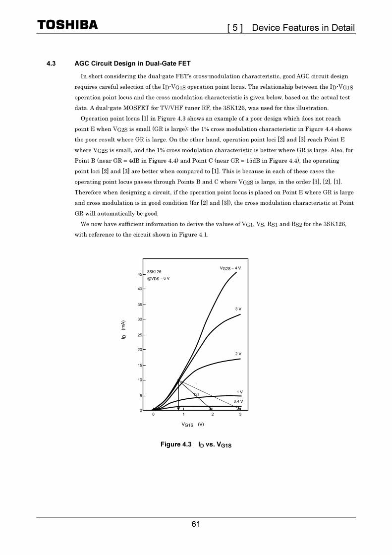
[ 5 ] Device Features in Detail
61
4.3 AGC Circuit Design in Dual-Gate FET
In short considering the dual-gate FET’s cross-modulation characteristic, good AGC circuit design
requires careful selection of the ID-VG1S operation point locus. The relationship between the ID-VG1S
operation point locus and the cross modulation characteristic is given below, based on the actual test
data. A dual-gate MOSFET for TV/VHF tuner RF, the 3SK126, was used for this illustration.
Operation point locus [1] in Figure 4.3 shows an example of a poor design which does not reach
point E when VG2S is small (GR is large); the 1% cross modulation characteristic in Figure 4.4 shows
the poor result where GR is large. On the other hand, operation point loci [2] and [3] reach Point E
where VG2S is small, and the 1% cross modulation characteristic is better where GR is large. Also, for
Point B (near GR = 4dB in Figure 4.4) and Point C (near GR = 15dB in Figure 4.4), the operating
point loci [2] and [3] are better when compared to [1]. This is because in each of these cases the
operating point locus passes through Points B and C where VG2S is large, in the order [3], [2], [1].
Therefore when designing a circuit, if the operation point locus is placed on Point E where GR is large
and cross modulation is in good condition (for [2] and [3]), the cross modulation characteristic at Point
GR will automatically be good.
We now have sufficient information to derive the values of VG1, VS, RS1 and RS2 for the 3SK126,
with reference to the circuit shown in Figure 4.1.
Figure 4.3 ID vs. VG1S
00
I D (m
A)
VG1S (V)
3SK126
@VDS = 6 V
0.4 V
1 V
2 V
3 V
VG2S = 4 V
[2]
[
1 2 3
5
10
15
20
25
30
35
40
45

[ 5 ] Device Features in Detail
62
Figure 4.4 1% Cross Modulation Characteristics
First, the FET must be completely in the OFF state, with VAGC = 0 V; Some allowance must be
made for variation in VS|ID = 0.
VS|ID = 0 = 1 − VG2S (OFF) (V)..................................................................... (1)
Next for VG1, VG1S (= VG1 − VS|ID = 0) is required to be at Point E, under the conditions of
VAGC = 0 and VS|ID = 0 = 1 − VG2S (OFF). When operation locus [3] in Figure 4.3 is used, VG1
becomes
VG1S = VG1S (OFF) + 3 V.............................................................................. (2)
Therefore,
VG1 = VG1S (OFF) + VS|ID = 0 + 3 V............................................................ (3)
When equation (1) is substituted in (3),
VG1 = 4 V + VG1S (OFF) (V).......................................................................... (4)
Also when GR = 0dB, VG2S = 3 V, and ID = 10 mA, one can determine VAGC max, RS1, and RS2 as
follows:
RS = RS1 RS2/(RS1 + RS2)............................................................................. (5)
VG1S|VG2S = 3 V, ID = 10 mA = VG1 − (VS|ID = 0 + RS × 10 mA).............. (6)
VG2S = VAGC max − (VS|ID = 0 + RS × 10 mA) = 3 (V)............................... (7)
and the design is completed by setting
RS = (VG1 − VS|ID = 0 − VG1S|VG2S = 3 V, ID = 10 mA)/10 mA (Ω) ........... (8)
VAGC max = 3 + VS|ID = 0 + RS × 10 mA (V) .............................................. (9)
Gain
re
duction
(d
B)
Undesired signal level (dBµ) 50 Ω Open
080
3SK126
Desired signal: 200 MHz
Undesired signal: 212 MHz
[1]
[2]
[3]
85 90 95 100 105
10
20
30
40
105 110 110
[ 5 ] Device Features in Detail
63
Using Figure 4.3 as a reference, when VG1S (OFF) = 0 V, VG2S (OFF) = 0 V, VGIS|VG2S = 3 V, and
ID = 10 mA = 0.92 V, the VS|ID = 0, VG1, RS, VAGC range becomes
VS|ID = 0 = 1 V
VG1 = 4 V
RS = 208 Ω
VAGC = 0 V to 6.08 V
Also, when VDS is under 6 V, GR = 0dB (VG2S = 3 V、ID = 10 mA), the value of VDD is found as
follows:
VDD = VS|ID = 0 + RS × 10 mA + VDS⎪VGS = 3 V, ID = 10 mA
= 1 V + 2.08 V + 6 V
= 9.08 V
Finally, RS1 and RS2 must be found:
RS = RS1 RS2/(RS1 + RS2) = 208 Ω ............................................................. (10)
VS|ID = 0 = VDD RS2/(RS1 + RS2) = 9.08 × RS2/(RS1 + RS2) = 1 V ............(11)
When equation (10) is divided by equation (11),
RS1/9.08 = 208
∴RS1 = 208 × 9.08 = 1.89 kΩ
Therefore, RS2 = 234 Ω
This completes the AGC circuit design for the dual-gate FET. Note that the cross-modulation
characteristics have been considered at each step.
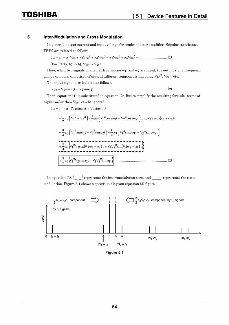
[ 5 ] Device Features in Detail
64
5. Inter-Modulation and Cross Modulation
In general, output current and input voltage for semiconductor amplifiers (bipolar transistors,
FETs) are related as follows:
IC = a0 + a1Vbe + a2Vbe2 + a3Vbe3 + a4Vbe4 + a5Vbe5 + ............................. (1)
(For FETs, IC ⇒ Id, Vbe ⇒ Vgs)
Here, when two signals of angular frequencies ω1, and ω2 are input, the output signal frequency
will be complex, comprised of several different components including Vbe2, Vbe3, etc.
The input signal is calculated as follows.
Vbe = V1sinω1t + V2sinω2t ........................................................................... (2)
Then, equation (1) is substituted in equation (2). But to simplify the resulting formula, terms of
higher order then Vbe3 can be ignored.
IC = a0 + a1 (V1sinω1t + V2sinω2t)
( ) tcosVVatcos2Vtcos2V a2
1 V V a
2
1212122
221
212
22
212 ωω±⎟
⎠⎞⎜
⎝⎛ ω+ω−⎟
⎠⎞⎜
⎝⎛ ++ m
⎟⎠⎞⎜
⎝⎛ ω+ω−⎟
⎠⎞⎜
⎝⎛ ω+ω+ tsin3Vtsin3V a
4
1 tsinVtsinV a
4
32
321
3132
321
313
( ) ( ) t2sinVVt2sinVVa4
312
221212
213 ω−ω+ω−ω+ mm
tsinVVtsinVVa2
31
22122
213 ω+ω+ ....................................................... (3)
In equation (3), represents the inter-modulation term and represents the cross
modulation. Figure 5.1 shows a spectrum diagram equation (3) figure.
Figure 5.1
f2 – f1
Level
2f1 – f2 2f2 – f1
2f1 2f2 3f1 3f20 f1 f2
2213 VVa
2
3 component
by f2 signals
110
2213 VVa
2
3 component by f1 signals
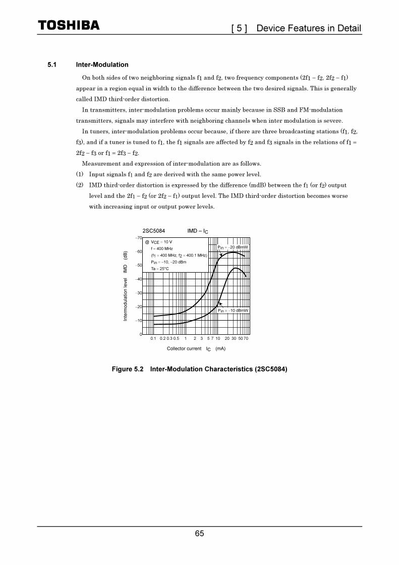
[ 5 ] Device Features in Detail
65
5.1 Inter-Modulation
On both sides of two neighboring signals f1 and f2, two frequency components (2f1 − f2, 2f2 − f1)
appear in a region equal in width to the difference between the two desired signals. This is generally
called IMD third-order distortion.
In transmitters, inter-modulation problems occur mainly because in SSB and FM-modulation
transmitters, signals may interfere with neighboring channels when inter modulation is severe.
In tuners, inter-modulation problems occur because, if there are three broadcasting stations (f1, f2,
f3), and if a tuner is tuned to f1, the f1 signals are affected by f2 and f3 signals in the relations of f1 =
2f2 − f3 or f1 = 2f3 − f2.
Measurement and expression of inter-modulation are as follows.
(1) Input signals f1 and f2 are derived with the same power level.
(2) IMD third-order distortion is expressed by the difference (mdB) between the f1 (or f2) output
level and the 2f1 − f2 (or 2f2 − f1) output level. The IMD third-order distortion becomes worse
with increasing input or output power levels.
Figure 5.2 Inter-Modulation Characteristics (2SC5084)
10.3 0.1 0
−10
−20
0.2
−30
−40
−50
−60
−70
Inte
rmod
ula
tion level
IM
D (d
B)
Collector current IC (mA)
@ VCE = 10 V
f = 400 MHz
(f1 = 400 MHz, f2 = 400.1 MHz)
Pin = −10, −20 dBm
Ta = 25°C
Pin = −20 dBmW
0.5 2 3 5 7 10 20 30 50 70
Pin = −10 dBmW
2SC5084 IMD – IC

[ 5 ] Device Features in Detail
66
5.2 Cross Modulation
When there are two neighboring signals f1 and f2, the f2 (or f1) signal affects f1 (or f2). For example,
when tuned by a non-modulated signal f1, the modulated f2 signal affects the f1 signal and creates f2
modulated signals in wave-detection output.
This problem arises in TV tuners when there are neighboring broadcasting stations f1 and f2. When
tuned to station f1, its video and audio signals are affected by the powerful station f2 video and audio
signals.
All illustration of measurement and expression of cross modulation follows:
(1) Example conditions: The desired signal is f1 and the undesired signal is f2, the f1 signal is
unmodulated and the f2 signal has 30% AM modulation at 1 kHz.
e1 = E1sinω1t
e2 = E2 (1 + m2cosωm2t) sinω2t
in which m2: undesired signal modulation ratio (0.3)
ωm2: modulation angular frequency (fm2 = 1 kHz)
(2) When signals e1 and e2 defined above are input, cross-modulation appears on the same frequency
as the desired signal, as shown by equation 3.
tsintmcosEma
a3 1 EaI 12
222
1
311C ω⎟
⎟⎠
⎞⎜⎜⎝
⎛ω⋅⋅+≈
As shown by the above equation, the required f1 signal (originally unmodulated) is modulated
by the undesired signal f2. The modulation ratio mK’ is defined by (or some such see next
question below) the following equation.
(percent)Ema
a3m 2
221
3K ⋅⋅⋅⋅=
The modulated signal is expressed by
IC = a1E1 1 + m1cosωm1 sinω1t
in which m1: desire signal modulation ratio (0.3)
ωm1: modulation angular frequency (fm1 = 1 kHz)
Therefore, the cross modulation exponent is
11
2223
1
KC
ma
Em3a
m
mK ==
In general, cross modulation is expressed by the level of the undesired signal E2 where
KC = 0.01. Therefore, when m1 = 0.3, m2 = 0.3,
3
12
a
a
300
1E ⋅=
This shows that E2 becomes larger if the distortion component is smaller (smaller a3), thus
lessening the interference problem.

[ 5 ] Device Features in Detail
67
6. Tape Packing Specifications
6.1 Tape Specifications by Type of Device Package
6.1.1 Super-Mini Package Group: S-MINI, SMQ, SMV (SSOP5-P-0.95) and SM6 (SSOP6-P-0.95)
Ultra-Super-Mini Package Group: USM, USQ, USV US6
Small Super-Mini (SSM)
Extremely Thin Super-Mini Package (TESM)
Ultra-Super-Mini and Thin Package (TU6)
Packing Type Tape Type Suffix Tape Dimensions (unit: mm) Reel Appearance Packing
Quantity
TE85L 3000 per reel
(Note 1)
Embossed tape
TE85L2 (only for s-mini, SMV and USM)
10000 per reel
Note 1: TESM: 4000 per reel.
6.1.2 Super-Mini Package for Varicap Diode
Packing Type Tape Type
Suffix Tape Dimensions (unit: mm) Reel Appearance Pair
Packing
Quantity
TPH2
TPH3 ×
TPH4
3000 per reel
TPH6 600 to 3000
per reel
Embossed tape
TPH7
3000 per reel
6.1.3 Ultra-Super-Mini Coaxial Package (USC)
Packing Type Tape Type
Suffix Tape Dimensions (unit: mm) Reel Appearance Pair
Packing
Quantity
TPH2 2400 to 3000
per reel
TPH3 × 3000 per reelEmbossed
tape
TPH4
2400 to 3000
per reel
44
8
44
8
44
8
Cathode

[ 5 ] Device Features in Detail
68
6.1.4 Extreme-Super-Mini Coaxial Package (ESC)
Extremely Thin Super-Mini Coaxial Package (TESC)
Packing Type Tape Type
Suffix Tape Dimensions (unit: mm) Reel Appearance Pair
Packing
Quantity
TPH2 3200 to 4000
per reel
TPH3
× 4000 per reel
TPL2 6400 to 8000
per reel
Embossed tape
TPL3
× 8000 per reel
6.1.5 Flat-Mini Package (FM8)
Packing Type Tape Type Suffix Tape Dimensions (unit: mm) Reel Appearance Packing
Quantity
Embossed tape
TE12L
1000 per reel
6.1.6 Flat-Super-Mini Package (SM8) (SSOP8-P-0.65)
Packing Type Tape Type Suffix Tape Dimensions (unit: mm) Reel Appearance Packing
Quantity
Embossed tape
TE12L
3000 per reel
12
4
4
12
8
2
8
Cathode
2
4
8
Cathode
4

[ 5 ] Device Features in Detail
69
6.1.7 Mini Package (MINI)
Packing Type Tape Type Suffix Tape Dimensions (unit: mm) Reel Appearance Packing
Quantity
Ammo pack TPE4
5000 per carton
6.1.8 Extreme-Super-Mini Package (ES6)
sES6
Packing Type Tape Type Suffix Tape Dimensions (unit: mm) Reel Appearance Packing
Quantity
Embossed tape
TE85L
4000 per reel
8
4
4
Feed-out
direction
Feed-out
direction 12.7
12.7

[ 5 ] Device Features in Detail
70
6.1.9 Extreme-Super-Mini Coaxial Package (sESC)
Packing Type Tape Type
Suffix Tape Dimensions (unit: mm) Reel Appearance Pair
Packing
Quantity
TPH3
× 5000 per reel
Embossed tape
TPL3
× 10000 per
reel
6.1.10 PW-X Package
Packing Type Tape Type
Suffix Tape Dimensions (unit: mm) Reel Appearance
Packing
Quantity
Embossed tape
TE12L
1000 per reel
2
8
Cathode
2
4
8
Cathode
4
4
12
[ 5 ] Device Features in Detail
71
6.1.11 Power Mini Transistor Package (PW-MINI)
Packing Type Tape Type
Suffix Tape Dimensions (unit: mm) Reel Appearance
Packing
Quantity
Tape
Pack type
TE12L
1000 per reel
Magazine
Stick type
⎯
25 per magazine
6.1.12 TO-92/Mini Devices
Tape Type Suffix Applied Package
Type Packing Type Packing Quantity Reel Appearance
TPE2 TO-92 (2-5F) Ammo pack 3000 pcs
TPE4 MINI (2-4E) Ammo pack 5000 pcs
6.1.13 Shrink Small Outline Package (SSOP20-P-225-1.0)
Packing Type Tape Type Suffix Tape Dimensions (unit: mm) Reel Appearance Packing
Quantity
Embossed tape
EL
2000 per reel
4.0 ± 0.1
12.0 ± 0.1
24.0
± 0
.3
Pin 1
4
8
12
178.2
10
7
[ 5 ] Device Features in Detail
72
6.2 Lead Formed TO-92 and Mini Transistor Package Dimensions
Snap forming: center lead
Figure 6.1 Lead-Formed TO-92 Transistor
Package Dimensions
Snap forming: center lead
Figure 6.2 Lead-Formed Mini
Transistor Package
Dimensions
Package No.2-5F106
5.1 max
4.1
max
2.5 ± 0.5 2.5 ± 0.5
4.7
max
4.5
± 0
.5
2.4
± 0
.5
Package No.2-5F108
2.5
5.1 max
2.5
4.1
max 0.4
5
2.4
5
4.7
max
2.4
1.0
4.5
0.45
4.5
2.1
2.4
0.65
Package No.2-4E101
4.0
0.4 4.5
2.1
1.9
0.8
4.2 max
3.2
max
6.4
2.4
0.3
2.5 2.5
2.6
max 1.0
5
Unit: mm

[ 5 ] Device Features in Detail
73
6.3 Tape Dimensions
6.3.1 Tape Layout for 3-Pin Super-Mini Package…(S-MINI)
This is a tape specification for 3-pin super mini-FETs and diodes. The diagram below shows the
TE85L tape specification.
New Tape Dimensions for Super-Mini Package Dimension Example: TE85L
Device Orientation
3.25
φ1.5 ± 0.1
4.0 ± 0.1
8.0
3.5
± 0
.05
3.3
1.7
5
0.25
1.35
Unit: mm
2.0 ± 0.05
[ 5 ] Device Features in Detail
74
6.3.2 Tape Layout for 4-Pin Super-Mini Package…(SMQ)
Device Orientation
2 13 4
φ1.5 ± 0.14.0 ± 0.1
8.0
3.5
± 0
.05
3.2
3
1.7
5
0.25
Unit: mm
3.2
1.32.0 ± 0.05
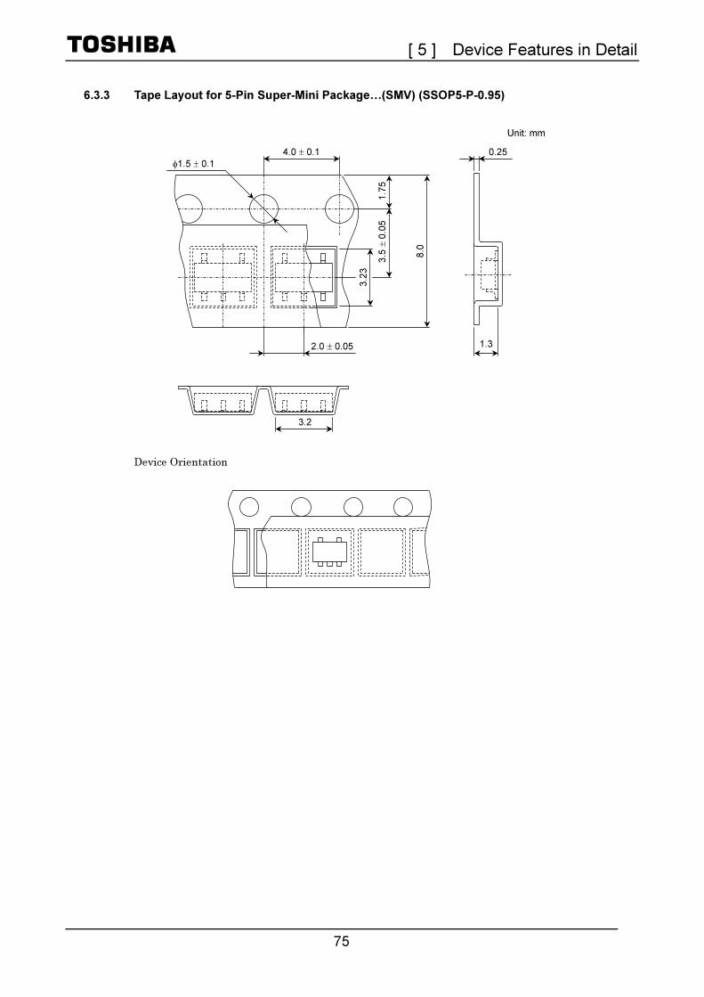
[ 5 ] Device Features in Detail
75
6.3.3 Tape Layout for 5-Pin Super-Mini Package…(SMV) (SSOP5-P-0.95)
Device Orientation
φ1.5 ± 0.1
4.0 ± 0.1
8.0
3.5
± 0
.05
3.2
3
1.7
5
Unit: mm
3.2
1.3
0.25
2.0 ± 0.05

[ 5 ] Device Features in Detail
76
6.3.4 Tape Layout for 6-Pin Super-Mini Package…(SM6) (SSOP6-P-0.95)
Device Orientation
L: TE85L
N: TE85N when there is no direction (Note)
Note: TE85N is tape packing of products which are symmetrical in both their internal
components and external leads, so that device orientation is unimportant.
Pin 1 is on lower left of the marking.
Example: Top View
6 4
321
5
A 1
Pin 1
A1
φ1.5 ± 0.14.0 ± 0.1
8.0
3.5
± 0
.05
3.2
3
1.7
5
Unit: mm
3.2
1.3
0.25
2.0 ± 0.05
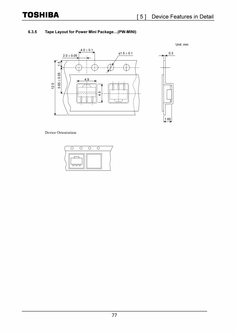
[ 5 ] Device Features in Detail
77
6.3.5 Tape Layout for Power Mini Package…(PW-MINI)
Device Orientation
4.0 ± 0.1 12.0
5.6
5 ±
0.0
5
φ1.5 ± 0.1
4.9
4.5
0.3
Unit: mm
1.65
1.5
2.0 ± 0.05

[ 5 ] Device Features in Detail
78
6.3.6 Tape Layout for Shrink Small Outline Package…(SSOP20-P-225)
A : 6.9 ± 0.2 mm
B : 10.5 ± 0.2 mm
C : 21.0 mm
D1 : 16.5 ± 0.1 mm
P1 : 12.0 ± 0.1 mm
T : 0.3 ± 0.1 mm
T1 : 2.2 ± 0.1 mm
Device Orientation
Pin 1
P1A 4.0 ± 0.1 Feed-out direction T2
Device recess φ1.5
φD1
17.5
± 0
.1
24.0
± 0
.3
11.5
± 0
.1
Slide view of product on tape
T
2.0 ± 0.1
+ 0.1− 0
Unit: mm
BC
A

[ 5 ] Device Features in Detail
79
6.3.7 Tape Layout for 3-Pin Ultra-Super-Mini Package…(USM)
Device Orientation
1.25 2.0 ± 0.05
φ1.5 ± 0.1 4.0 ± 0.1
8.0
3.5
± 0
.05
2.3
1.7
5
0.2
Unit: mm
2.2
1.0
1.1

[ 5 ] Device Features in Detail
80
6.3.8 Tape Layout for 4-Pin Ultra-Super-Mini Package…(USQ)
Device Orientation
MN
φ1.5 ± 0.1 4.0 ± 0.1
8.0
3.5
± 0
.05
2.3
1.7
5
0.25
Unit: mm
2.2
φ1.1
A
B’B
A’
B’B
A
1.2 A’
2.0 ± 0.05
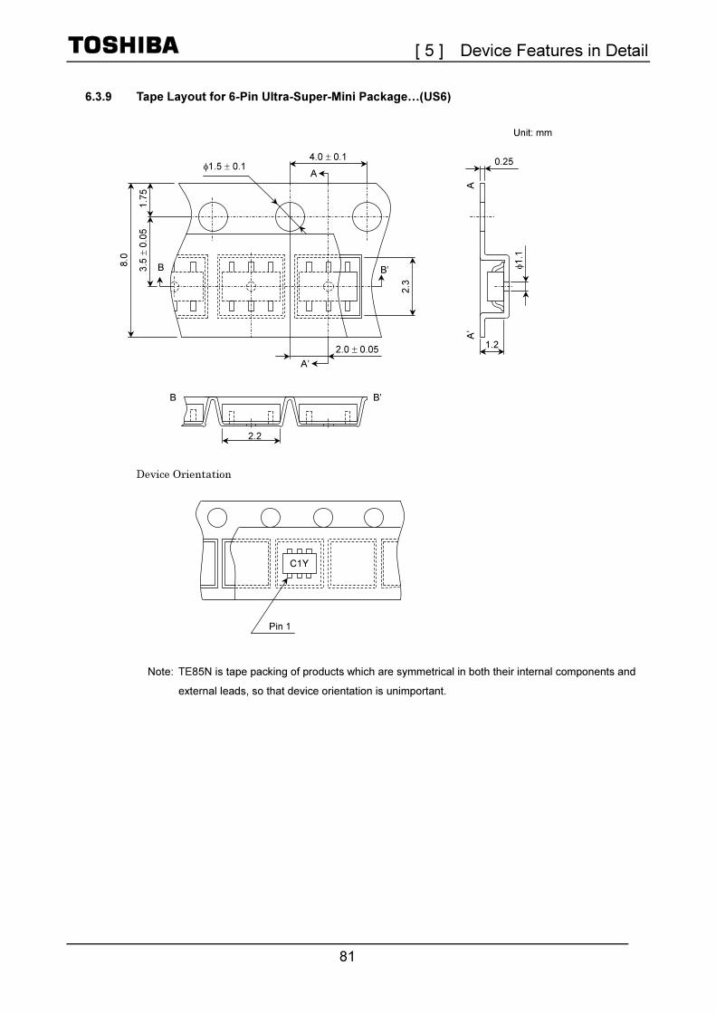
[ 5 ] Device Features in Detail
81
6.3.9 Tape Layout for 6-Pin Ultra-Super-Mini Package…(US6)
Device Orientation
Note: TE85N is tape packing of products which are symmetrical in both their internal components and
external leads, so that device orientation is unimportant.
Pin 1
C1Y
φ1.5 ± 0.1 4.0 ± 0.1
8.0
3.5
± 0
.05
2.3
1.7
5
0.25
Unit: mm
2.2
φ1.1
A
B’B
A’
B’B
A
1.2
A’
2.0 ± 0.05
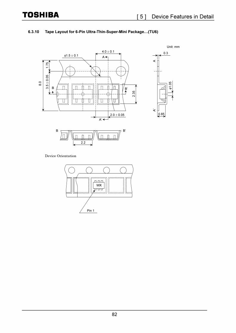
[ 5 ] Device Features in Detail
82
6.3.10 Tape Layout for 6-Pin Ultra-Thin-Super-Mini Package…(TU6)
Device Orientation
Pin 1
WX
φ1.5 ± 0.1
4.0 ± 0.1
2.0 ± 0.05
8.0
3.5
± 0
.05
2.3
5
1.7
5
0.3
Unit: mm
2.2
φ1.0
5
A
B’B
A’
B’B
A
0.85
A’

[ 5 ] Device Features in Detail
83
6.3.11 Tape Layout for Small-Super-Mini Package…(SSM)
Device Orientation
2.0 ± 0.05
φ1.5 ± 0.1 4.0 ± 0.1
8.0
3.5
± 0
.05
1.8
1.7
5
0.2
Unit: mm
1.75
φ0.5
A
B’B
A’
B’B
A
0.95 A’
0.6
1.3
5

[ 5 ] Device Features in Detail
84
6.3.12 Tape Layout for Ultra-Super-Mini Coaxial Package…(USC)
Device Orientation
Correct device orientation
1.3φ1.5 ± 0.1
4.0 ± 0.1
8.0
3.5
± 0
.05
1.7
5
0.27
Unit: mm
2.7
5
φ1.0
5
1.12.0 ± 0.05
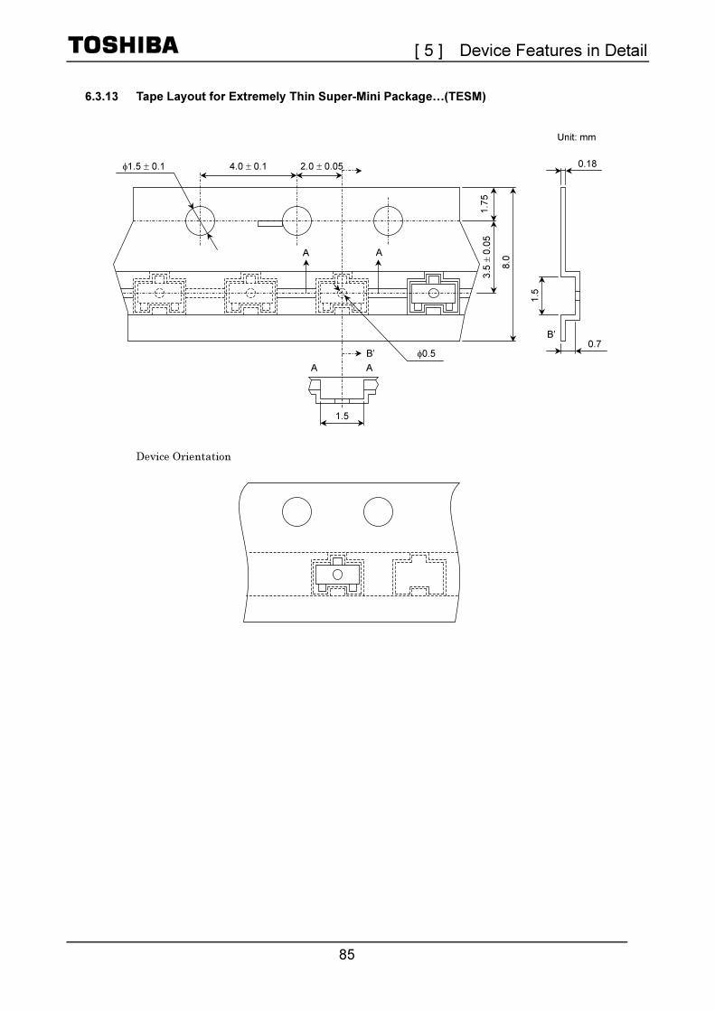
[ 5 ] Device Features in Detail
85
6.3.13 Tape Layout for Extremely Thin Super-Mini Package…(TESM)
Device Orientation
φ1.5 ± 0.1
3.5
± 0
.05
4.0 ± 0.1 2.0 ± 0.05
φ0.5
A A
1.5
A A
8.0
1.7
5
0.18
0.7
1.5
Unit: mm
B’
B’
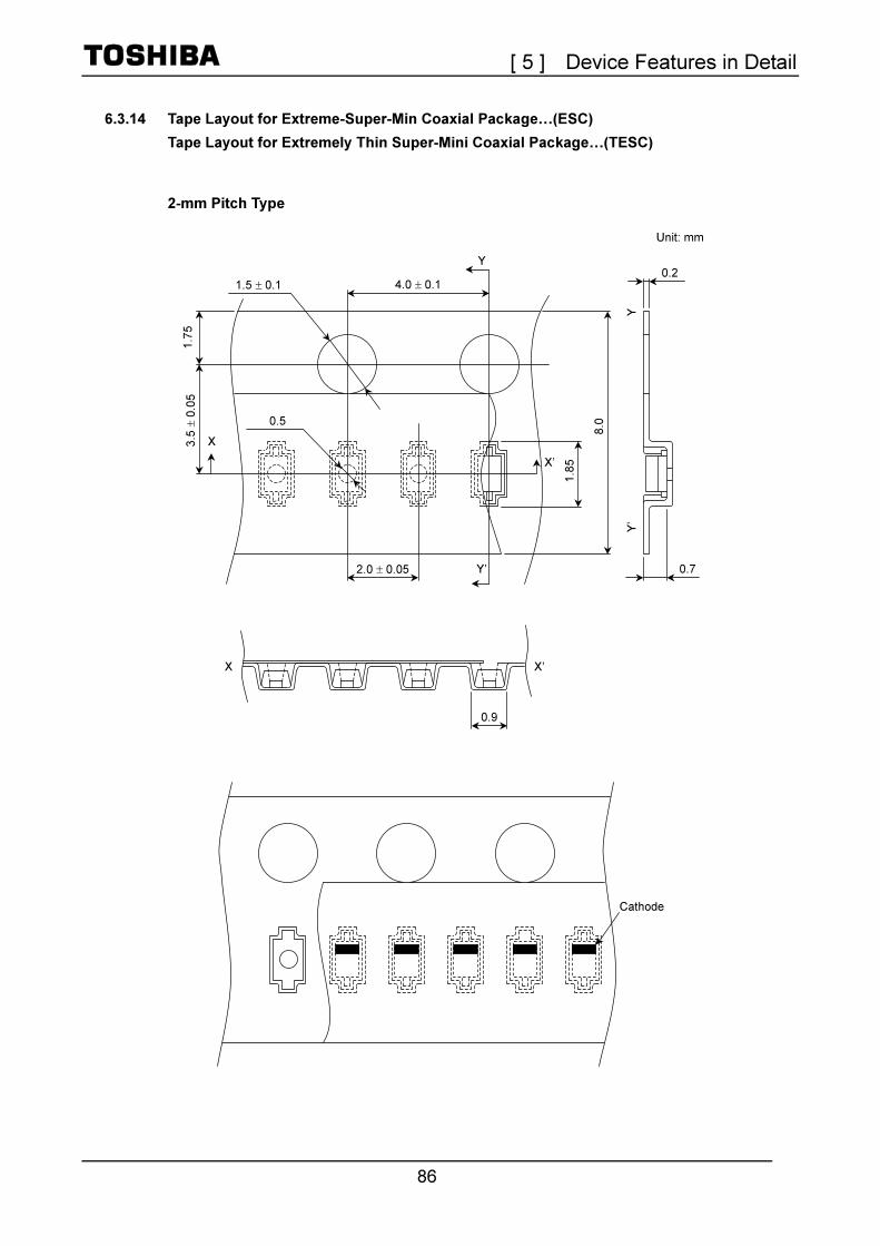
[ 5 ] Device Features in Detail
86
6.3.14 Tape Layout for Extreme-Super-Min Coaxial Package…(ESC)
Tape Layout for Extremely Thin Super-Mini Coaxial Package…(TESC)
2-mm Pitch Type
Cathode
0.9
X’X
4.0 ± 0.1
1.7
5
1.5 ± 0.1
2.0 ± 0.05
0.2
3.5
± 0
.05
X
Y’
X’
1.8
5
Y
Y’
0.7
8.0
Y
0.5
Unit: mm

[ 5 ] Device Features in Detail
87
4-mm Pitch Type
Cathode
0.9
X’X
4.0 ± 0.1
1.7
5
1.5 ± 0.1
0.2
3.5
± 0
.05
X
Y’
X’
1.8
5
Y
Y’
0.7
8.0
Y
0.5
2.0 ± 0.05
Unit: mm
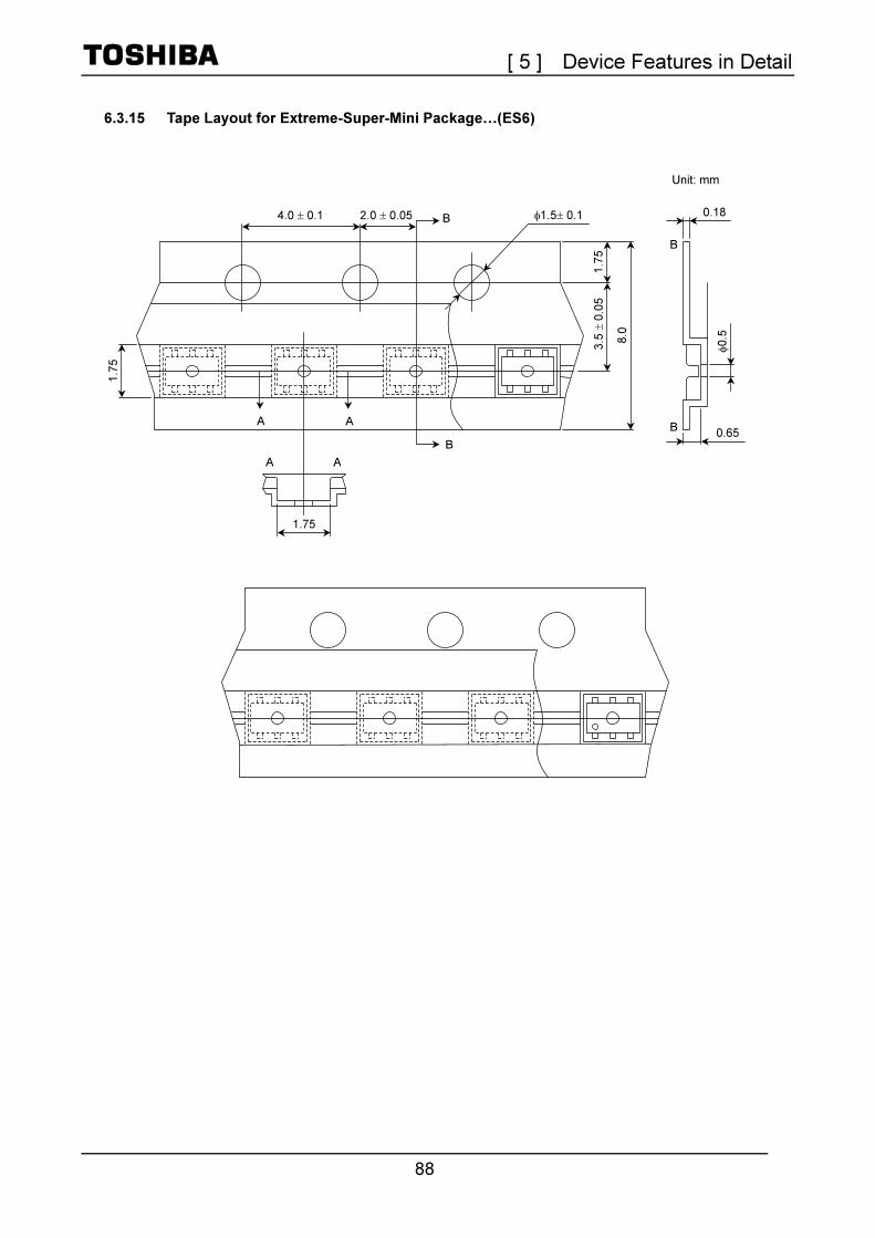
[ 5 ] Device Features in Detail
88
6.3.15 Tape Layout for Extreme-Super-Mini Package…(ES6)
φ1.5± 0.1
3.5
± 0
.05
4.0 ± 0.1 2.0 ± 0.05
1.75
A A
A A
1.7
5
0.18
0.65
1.7
5
Unit: mm
B
B
B
B
φ0.5
8.0
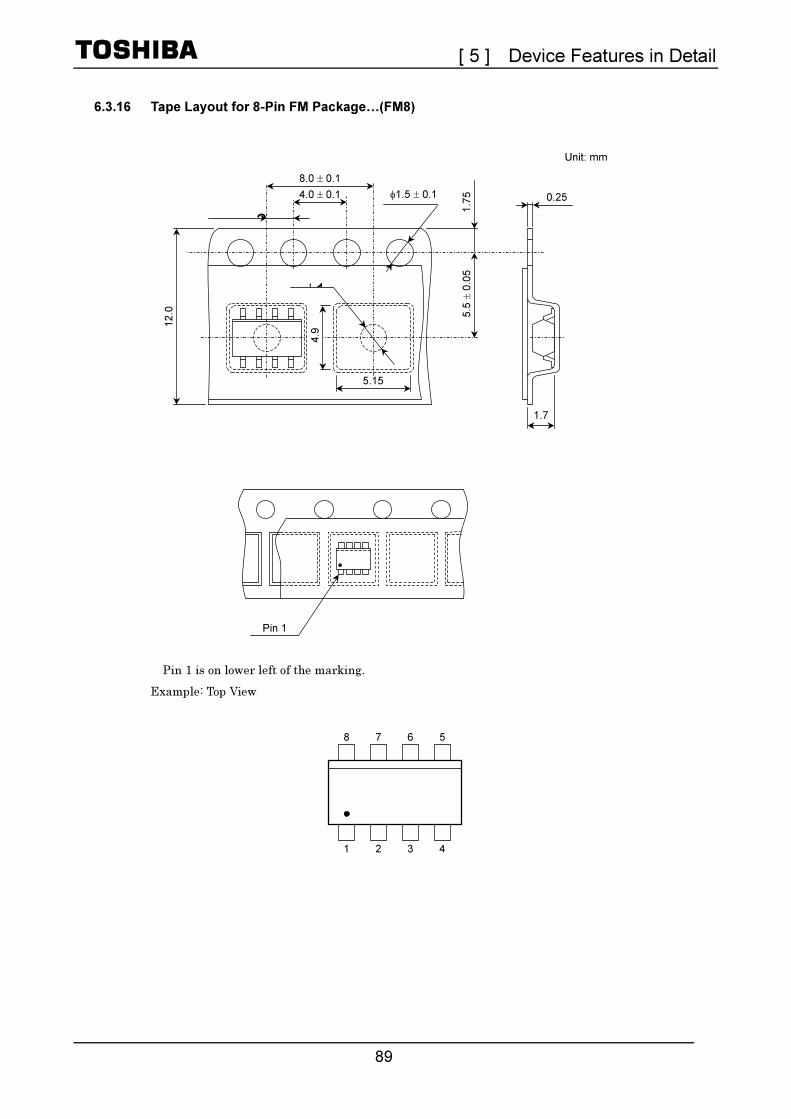
[ 5 ] Device Features in Detail
89
6.3.16 Tape Layout for 8-Pin FM Package…(FM8)
Pin 1 is on lower left of the marking.
Example: Top View
Pin 1
8 6
321
7
5
4
4.9
8.0 ± 0.1
4.0 ± 0.1
2
φ1
φ1.5 ± 0.1 0.25
1.7
5.15
5.5
± 0
.05
1.7
5
Unit: mm 12.0

[ 5 ] Device Features in Detail
90
6.3.17 Tape Layout for 8-Pin SM Package…(SM8)
Pin 1
φ1.5 ± 0.1
4.4
φ1.05
4.0 ± 0.1
3.1
2.0 ± 0.055.5
± 0
.05
1.7
5
12.0
0.3
1.55
Unit: mm

[ 5 ] Device Features in Detail
91
6.3.18 Tape Layout for PW-X Package…(PW-X)
5.1
4.9
6.4
1.0
1.4
12.0
5.5
± 0
.05
1.7
5
2.0 ± 0.05
4.0 ± 0.1
A
φ1.5 ± 0.1
φ1.55
0.3
1.65
A
A’
6.6
Unit: mm
8.0 ± 0.1
A’
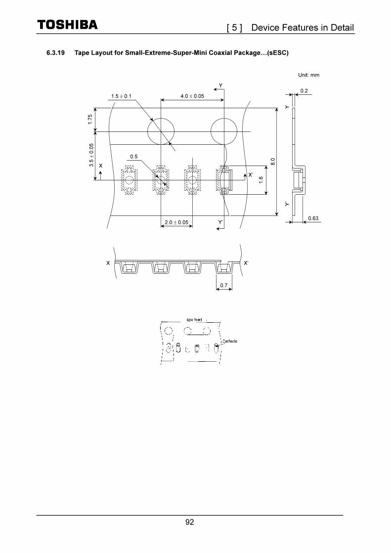
[ 5 ] Device Features in Detail
92
6.3.19 Tape Layout for Small-Extreme-Super-Mini Coaxial Package…(sESC)
0.7
X’X
4.0 ± 0.05
1.7
5
1.5 ± 0.1
2.0 ± 0.05
0.2 3.5
± 0
.05
X
Y’
X’
1.6
Y
Y’
8.0
Y
0.5
Unit: mm
0.63
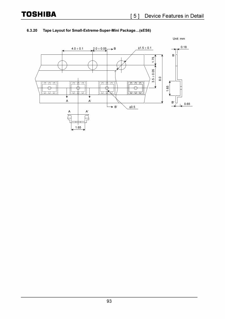
[ 5 ] Device Features in Detail
93
6.3.20 Tape Layout for Small-Extreme-Super-Mini Package…(sES6)
1.65
φ1.5 ± 0.1
3.5
± 0
.05
4.0 ± 0.1 2.0 ± 0.05
φ0.5
A A’
A A’
1.7
5
0.18
0.65
1.6
5
Unit: mm
B’
B
B
B’
8.0
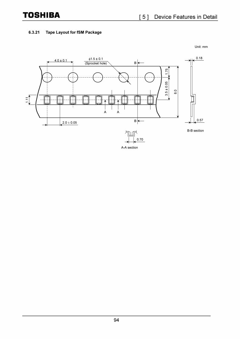
[ 5 ] Device Features in Detail
94
6.3.21 Tape Layout for fSM Package
Unit: mm
0.18
0.57
B-B section
8.0
3.5
± 0
.05
φ1.5 ± 0.1
(Sprocket hole) B4.0 ± 0.1
A A
B
1.7
5
A-A section
0.70
1.1
1
2.0 ± 0.05
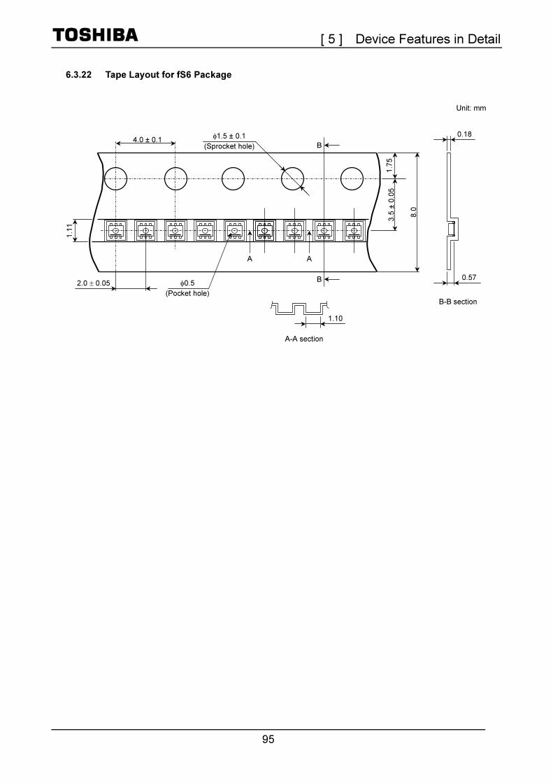
[ 5 ] Device Features in Detail
95
6.3.22 Tape Layout for fS6 Package
Unit: mm
1.10
A-A section
B-B section
0.18
0.57
8.0
3.5
± 0
.05
φ1.5 ± 0.1
(Sprocket hole) B4.0 ± 0.1
φ0.5
(Pocket hole)
A A
B
1.7
5
1.1
1
2.0 ± 0.05

[ 5 ] Device Features in Detail
96
6.3.23 Tape Layout for fSC Package
Tape Specifications
1 Cumulative pitch error tolerance is ±0.2 mm/10 devices.
2 Tape meterial is plastic (anti-electrostatic).
3 Tape dimensions.
Unit: mm
0.70
A-A section
B-B section
1.1
1
0.18
0.57
8.0
3.5
± 0
.05
φ1.5 ± 0.1
(Sprocket hole) B4.0 ± 0.05
Cathode
A A
B
1.7
5
2.0 ± 0.05

[ 5 ] Device Features in Detail
97
6.3.24 Radial Tape Layout for TO-92 and Mini Package
Dimensions Unit: mm
Measurement Symbol TO-92
(SC-43) MINI TO-92MOD MSTM
Remarks
Product Width A1 6.0 max 4.5 max 5.1 max 7.1 max
Product Height A 9.0 max 3.5 max 8.2 max 4.7 max
Product Thickness T 6.0 max 2.6 max 4.1 max 2.7 max
Lead Width d 0.45
typ. 0.4
typ. 0.67
max 0.45
typ.
Please refer to each technical datasheet for more details
Attached Lead Length 1l 2.5 min 3.5 min 2.6 min
Pitch Between Products P 12.7 ± 1.0 12.7 ± 0.5
Feed Hole Pitch P0 12.7 ± 0.3 12.7 ± 0.2 Cumulative pitch error rate: ±1 mm/20 pitches
Feed Hole Center to Lead Center
P2 6.35 ± 0.4
Lead Spacing F1/F2 2.5 2.54
Vertical Skew ∆h 0 ± 2.0 0 ± 1.0
Tape Width W 18.0
Sealing Tape Width W0 6.0 ± 0.3
Tape Edge to Feed Hole Center
W1 9.0 9.0 ± 0.5
Carrier Tape Edge to Sealing Tape Edge
W3 0.5 max
Package to Feed Hole Center
H 20 max 20 20 max 19 ± 0.5
Lead Clinch to Feed Hole Center
H0 16.0 ± 0.5 ⎯
Product Protrusion from Feed Hole Center
H1 32.25 max 25.0 max
Feed Hole Diameter D0 4.0 ± 0.2
Tape Thickness t 0.6 ± 0.2
Length of Shipped Lead L1 11.0 max
Horizontal Skew ∆P 0 ± 1.0
L1
P0
P2
F1 F2
P
A1
A
H0
H1
H
W0
W1
W
D0
W2
T
d
∆P ∆h
1l1l
t
+ 1.0− 0.5
+ 0.75− 0.5
+ 0.75− 0.5
+ 0.6− 0.3
+ 0.3− 0.2

[ 5 ] Device Features in Detail
98
Ammo Pack and Ammo Pack Dimensions
Unit: mm
Package Type W H D
TO-92 (SC-43) 336 ± 3 250 ± 3 47 ± 3
MINI 336 ± 3 260 ± 3 47 ± 3
TO-92MOD 336 ± 3 190 ± 3 47 ± 3
MSTM 336 ± 3 230 ± 3 47 ± 3
*: Indicate the first electrode of a lead
Example: E: Emitter
B: Base
BCE
Remove at least 4 products
One row consists of 25 products D
H
W*B
BCE
E*

[ 5 ] Device Features in Detail
99
7. Reference Pad Dimensions
The following shows reference pad dimensions when a device mounted on a board. Unit: mm
(1) 3-pin extremely thin super-mini
package (TESM)
(2) 3-pin small-super-mini package (SSM)
(3) 3-pin ultra-super-mini package (USM)
(JEITA: SC-70)
(4) 3-pin super-mini package (SM)
(JEITA: SC-59)
0.5
0.55
1.1
0.5
0.5
0.9
0.6
0.6
1.4
0.5 0.5
0.65
1.0
0.65
0.6
1.9
0.95 0.95
0.8
1.0
2.4

[ 5 ] Device Features in Detail
100
Unit: mm
(5) 4-pin ultra-super-mini package (USQ) (6) 4-Pin super-mini package (SMQ)
(JEITA: SC-61B)
(7) 5-pin super-mini package (5LEAD)
(SMV)
(8) 6-pin super-mini (SM6)
0.1
1.9
1.45
1.3
5
0.9
2.4
0.9
0.9
0.6
0.95
2.4
0.8 0.8
1.0
0.95 (SSOP5-P-0.95)
0.6
0.95
2.4
0.8 0.8
1.0
0.95 (SSOP6-P-0.95)
1.3
1.9
1.0
0.6
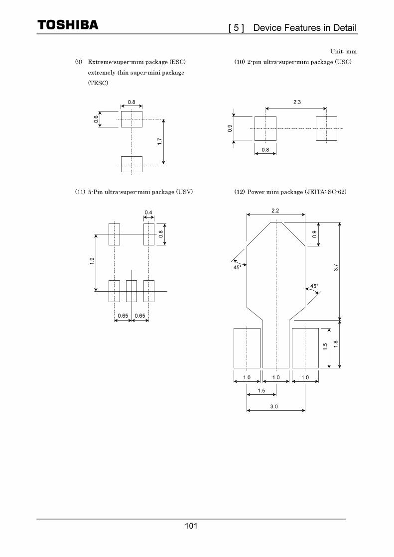
[ 5 ] Device Features in Detail
101
Unit: mm
(9) Extreme-super-mini package (ESC)
extremely thin super-mini package
(TESC)
(10) 2-pin ultra-super-mini package (USC)
(11) 5-Pin ultra-super-mini package (USV) (12) Power mini package (JEITA: SC-62)
2.2
3.7
1.5
1.8
0.9
3.0
45°
45°
1.0 1.0 1.0
1.5
0.9
0.8
2.3
0.6
0.8
1.7
1.9
0.65 0.65
0.8
0.4
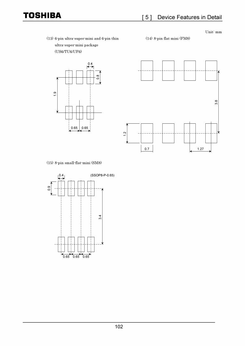
[ 5 ] Device Features in Detail
102
Unit: mm
(13) 6-pin ultra-super-mini and 6-pin thin
ultra-super-mini package
(US6/TU6/UF6)
(14) 8-pin flat mini (FM8)
(15) 8-pin small-flat-mini (SM8)
0.4
0.65 0.65
0.9
0.65
3.4
(SSOP8-P-0.65)
0.7
3.8
1.2
1.27
1.9
0.65 0.65
0.8
0.4
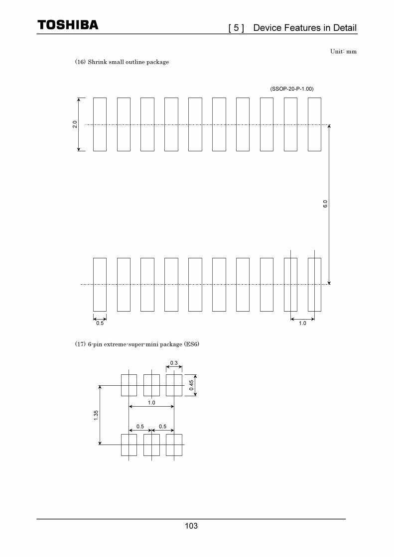
[ 5 ] Device Features in Detail
103
Unit: mm
(16) Shrink small outline package
(17) 6-pin extreme-super-mini package (ES6)
0.5
2.0
6.0
1.0
(SSOP-20-P-1.00)
1.3
5
1.0
0.3
0.5
0.4
5
0.5
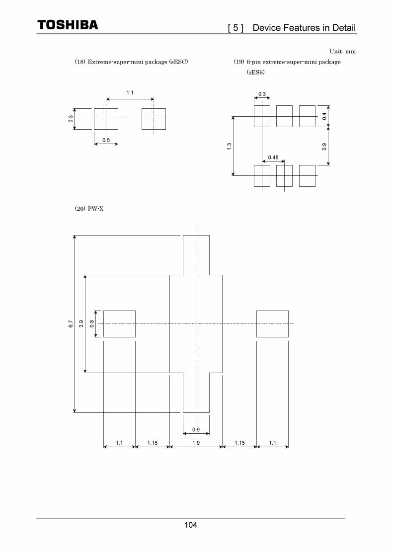
[ 5 ] Device Features in Detail
104
Unit: mm
(18) Extreme-super-mini package (sESC) (19) 6-pin extreme-super-mini package
(sES6)
(20) PW-X
1.3
0.3
0.48
0.4
0.9
6.7
0.8
0.9
1.9 1.15
3.9
1.11.15 1.1
0.3
0.5
1.1

[ 5 ] Device Features in Detail
105
The following shows reference pad dimensions when a device mounted on a board. Unit: mm
(21) fSM (22) fS6
(23) fSC
0.1
7
1.0
4
0.1
7
0.7
0.35 0.35
0.19
0.24
0.1
9
0.6
6
0.1
9
0.19 0.16
0.35
0.8
5
0.2
6
0.21
0.85


[ 6 ] Handling Precautions


[ 6 ] Handling Precautions
109
[ 6 ] Handling Precautions
1. Using Toshiba Semiconductors Safely
TOSHIBA is continually working to improve the quality and reliability of its products. Nevertheless,
semiconductor devices in general can malfunction or fail due to their inherent electrical sensitivity
and vulnerability to physical stress. It is the responsibility of the buyer, when utilizing TOSHIBA
products, to comply with the standards of safety in making a safe design for the entire system, and to
avoid situations in which a malfunction or failure of such TOSHIBA products could cause loss of
human life, bodily injury or damage to property.
In developing your designs, please ensure that TOSHIBA products are used within specified
operating ranges as set forth in the most recent TOSHIBA products specifications. Also, please keep
in mind the precautions and conditions set forth in the “Handling Guide for Semiconductor Devices,”
or “TOSHIBA Semiconductor Reliability Handbook” etc..
The TOSHIBA products listed in this document are intended for usage in general electronics
applications (computer, personal equipment, office equipment, measuring equipment, industrial
robotics, domestic appliances, etc.). These TOSHIBA products are neither intended nor warranted for
usage in equipment that requires extraordinarily high quality and/or reliability or a malfunction or
failure of which may cause loss of human life or bodily injury (“Unintended Usage”). Unintended
Usage include atomic energy control instruments, airplane or spaceship instruments, transportation
instruments, traffic signal instruments, combustion control instruments, medical instruments, all
types of safety devices, etc.. Unintended Usage of TOSHIBA products listed in this document shall be
made at the customer’s own risk.

[ 6 ] Handling Precautions
110
2. Safety Precautions
This section lists important precautions which users of semiconductor devices (and anyone else)
should observe in order to avoid injury and damage to property, and to ensure safe and correct use of
devices.
Please be sure that you understand the meanings of the labels and the graphic symbol described
below before you move on to the detailed descriptions of the precautions.
[Explanation of Labels]
Indicates an imminently hazardous situation which will result in death or serious injury if you do not follow instructions.
Indicates a potentially hazardous situation which could result in death or serious injury if you do not follow instructions.
Indicates a potentially hazardous situation which if not avoided, may result in minor injury or moderate injury.

[ 6 ] Handling Precautions
111
2.1 General Precautions Regarding Semiconductor Devices
Do not use devices under conditions exceeding their absolute maximum ratings (e.g. current, voltage, power dissipation or temperature).
This may cause the device to break down, degrade its performance, or cause it to catch fire or explode resulting in injury.
Do not insert devices in the wrong orientation.
Make sure that the positive and negative terminals of power supplies are connected correctly. Otherwise the rated maximum current or power dissipation may be exceeded and the device may break down or undergo performance degradation, causing it to catch fire or explode and resulting in injury.
When power to a device is on, do not touch the device’s heat sink.
Heat sinks become hot, so you may burn your hand.
Do not touch the tips of device leads.
Because some types of device have leads with pointed tips, you may prick your finger.
When conducting any kind of evaluation, inspection or testing, be sure to connect the testing equipment’s electrodes or probes to the pins of the device under test before powering it on.
Otherwise, you may receive an electric shock causing injury.
Before grounding an item of measuring equipment or a soldering iron, check that there is no electrical leakage from it.
Electrical leakage may cause the device which you are testing or soldering to break down, or could give you an electric shock.
Always wear protective glasses when cutting the leads of a device with clippers or a similar tool.
If you do not, small bits of metal flying off the cut ends may damage your eyes.
2.2 Bipolar ICs (for use in automobiles)
If your design includes an inductive load such as a motor coil, incorporate diodes or similar devices into the design to prevent negative current from flowing in.
The load current generated by powering the device on and off may cause it to function erratically or to break down, which could in turn cause injury.
Ensure that the power supply to any device which incorporates protective functions is stable.
If the power supply is unstable, the device may operate erratically, preventing the protective functions from working correctly. If protective functions fail, the device may break down causing injury to the user.
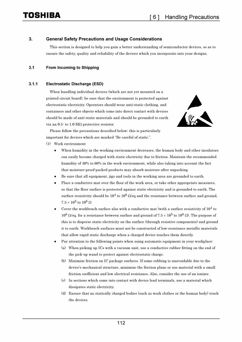
[ 6 ] Handling Precautions
112
3. General Safety Precautions and Usage Considerations
This section is designed to help you gain a better understanding of semiconductor devices, so as to
ensure the safety, quality and reliability of the devices which you incorporate into your designs.
3.1 From Incoming to Shipping
3.1.1 Electrostatic Discharge (ESD)
When handling individual devices (which are not yet mounted on a
printed circuit board), be sure that the environment is protected against
electrostatic electricity. Operators should wear anti-static clothing, and
containers and other objects which come into direct contact with devices
should be made of anti-static materials and should be grounded to earth
via an 0.5- to 1.0-MΩ protective resistor.
Please follow the precautions described below; this is particularly
important for devices which are marked “Be careful of static.”.
(1) Work environment
When humidity in the working environment decreases, the human body and other insulators
can easily become charged with static electricity due to friction. Maintain the recommended
humidity of 40% to 60% in the work environment, while also taking into account the fact
that moisture-proof-packed products may absorb moisture after unpacking.
Be sure that all equipment, jigs and tools in the working area are grounded to earth.
Place a conductive mat over the floor of the work area, or take other appropriate measures,
so that the floor surface is protected against static electricity and is grounded to earth. The
surface resistivity should be 104 to 108 Ω/sq and the resistance between surface and ground,
7.5 × 10⁵ to 108 Ω
Cover the workbench surface also with a conductive mat (with a surface resistivity of 104 to
108 Ω/sq, for a resistance between surface and ground of 7.5 × 10⁵ to 108 Ω). The purpose of
this is to disperse static electricity on the surface (through resistive components) and ground
it to earth. Workbench surfaces must not be constructed of low-resistance metallic materials
that allow rapid static discharge when a charged device touches them directly.
Pay attention to the following points when using automatic equipment in your workplace:
(a) When picking up ICs with a vacuum unit, use a conductive rubber fitting on the end of
the pick-up wand to protect against electrostatic charge.
(b) Minimize friction on IC package surfaces. If some rubbing is unavoidable due to the
device’s mechanical structure, minimize the friction plane or use material with a small
friction coefficient and low electrical resistance. Also, consider the use of an ionizer.
(c) In sections which come into contact with device lead terminals, use a material which
dissipates static electricity.
(d) Ensure that no statically charged bodies (such as work clothes or the human body) touch
the devices.
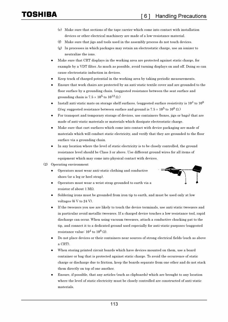
[ 6 ] Handling Precautions
113
(e) Make sure that sections of the tape carrier which come into contact with installation
devices or other electrical machinery are made of a low-resistance material.
(f) Make sure that jigs and tools used in the assembly process do not touch devices.
(g) In processes in which packages may retain an electrostatic charge, use an ionizer to
neutralize the ions.
Make sure that CRT displays in the working area are protected against static charge, for
example by a VDT filter. As much as possible, avoid turning displays on and off. Doing so can
cause electrostatic induction in devices.
Keep track of charged potential in the working area by taking periodic measurements.
Ensure that work chairs are protected by an anti-static textile cover and are grounded to the
floor surface by a grounding chain. (suggested resistance between the seat surface and
grounding chain is 7.5 × 10⁵ to 1012 Ω.)
Install anti-static mats on storage shelf surfaces. (suggested surface resistivity is 104 to 108
Ω/sq; suggested resistance between surface and ground is 7.5 × 10⁵ to 108 Ω.)
For transport and temporary storage of devices, use containers (boxes, jigs or bags) that are
made of anti-static materials or materials which dissipate electrostatic charge.
Make sure that cart surfaces which come into contact with device packaging are made of
materials which will conduct static electricity, and verify that they are grounded to the floor
surface via a grounding chain.
In any location where the level of static electricity is to be closely controlled, the ground
resistance level should be Class 3 or above. Use different ground wires for all items of
equipment which may come into physical contact with devices.
(2) Operating environment
Operators must wear anti-static clothing and conductive
shoes (or a leg or heel strap).
Operators must wear a wrist strap grounded to earth via a
resistor of about 1 MΩ.
Soldering irons must be grounded from iron tip to earth, and must be used only at low
voltages (6 V to 24 V).
If the tweezers you use are likely to touch the device terminals, use anti-static tweezers and
in particular avoid metallic tweezers. If a charged device touches a low-resistance tool, rapid
discharge can occur. When using vacuum tweezers, attach a conductive chucking pat to the
tip, and connect it to a dedicated ground used especially for anti-static purposes (suggested
resistance value: 104 to 108 Ω).
Do not place devices or their containers near sources of strong electrical fields (such as above
a CRT).
When storing printed circuit boards which have devices mounted on them, use a board
container or bag that is protected against static charge. To avoid the occurrence of static
charge or discharge due to friction, keep the boards separate from one other and do not stack
them directly on top of one another.
Ensure, if possible, that any articles (such as clipboards) which are brought to any location
where the level of static electricity must be closely controlled are constructed of anti-static
materials.
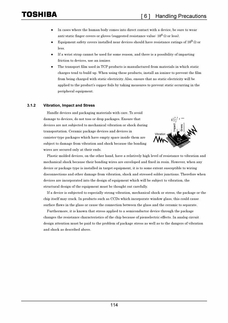
[ 6 ] Handling Precautions
114
In cases where the human body comes into direct contact with a device, be sure to wear
anti-static finger covers or gloves (suggested resistance value: 108 Ω or less).
Equipment safety covers installed near devices should have resistance ratings of 109 Ω or
less.
If a wrist strap cannot be used for some reason, and there is a possibility of imparting
friction to devices, use an ionizer.
The transport film used in TCP products is manufactured from materials in which static
charges tend to build up. When using these products, install an ionizer to prevent the film
from being charged with static electricity. Also, ensure that no static electricity will be
applied to the product’s copper foils by taking measures to prevent static occurring in the
peripheral equipment.
3.1.2 Vibration, Impact and Stress
Handle devices and packaging materials with care. To avoid
damage to devices, do not toss or drop packages. Ensure that
devices are not subjected to mechanical vibration or shock during
transportation. Ceramic package devices and devices in
canister-type packages which have empty space inside them are
subject to damage from vibration and shock because the bonding
wires are secured only at their ends.
Plastic molded devices, on the other hand, have a relatively high level of resistance to vibration and
mechanical shock because their bonding wires are enveloped and fixed in resin. However, when any
device or package type is installed in target equipment, it is to some extent susceptible to wiring
disconnections and other damage from vibration, shock and stressed solder junctions. Therefore when
devices are incorporated into the design of equipment which will be subject to vibration, the
structural design of the equipment must be thought out carefully.
If a device is subjected to especially strong vibration, mechanical shock or stress, the package or the
chip itself may crack. In products such as CCDs which incorporate window glass, this could cause
surface flaws in the glass or cause the connection between the glass and the ceramic to separate.
Furthermore, it is known that stress applied to a semiconductor device through the package
changes the resistance characteristics of the chip because of piezoelectric effects. In analog circuit
design attention must be paid to the problem of package stress as well as to the dangers of vibration
and shock as described above.
Vibration
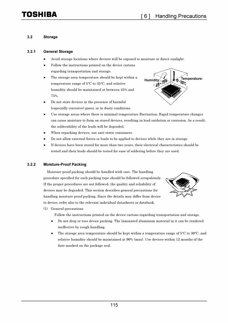
[ 6 ] Handling Precautions
115
3.2 Storage
3.2.1 General Storage
Avoid storage locations where devices will be exposed to moisture or direct sunlight.
Follow the instructions printed on the device cartons
regarding transportation and storage.
The storage area temperature should be kept within a
temperature range of 5°C to 35°C, and relative
humidity should be maintained at between 45% and
75%.
Do not store devices in the presence of harmful
(especially corrosive) gases, or in dusty conditions.
Use storage areas where there is minimal temperature fluctuation. Rapid temperature changes
can cause moisture to form on stored devices, resulting in lead oxidation or corrosion. As a result,
the solderability of the leads will be degraded.
When repacking devices, use anti-static containers.
Do not allow external forces or loads to be applied to devices while they are in storage.
If devices have been stored for more than two years, their electrical characteristics should be
tested and their leads should be tested for ease of soldering before they are used.
3.2.2 Moisture-Proof Packing
Moisture-proof packing should be handled with care. The handling
procedure specified for each packing type should be followed scrupulously.
If the proper procedures are not followed, the quality and reliability of
devices may be degraded. This section describes general precautions for
handling moisture-proof packing. Since the details may differ from device
to device, refer also to the relevant individual datasheets or databook.
(1) General precautions
Follow the instructions printed on the device cartons regarding transportation and storage.
Do not drop or toss device packing. The laminated aluminum material in it can be rendered
ineffective by rough handling.
The storage area temperature should be kept within a temperature range of 5°C to 30°C, and
relative humidity should be maintained at 90% (max). Use devices within 12 months of the
date marked on the package seal.
Humidity: Temperature:
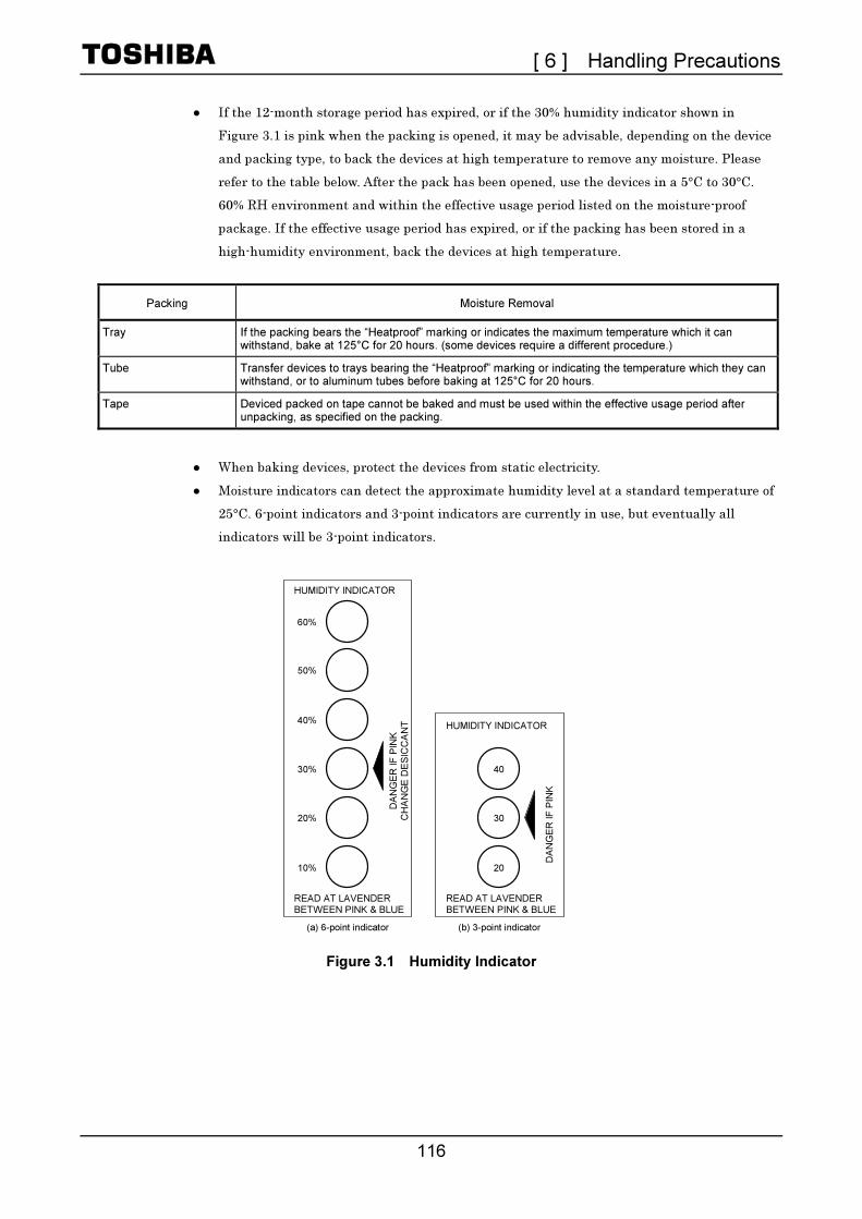
[ 6 ] Handling Precautions
116
If the 12-month storage period has expired, or if the 30% humidity indicator shown in
Figure 3.1 is pink when the packing is opened, it may be advisable, depending on the device
and packing type, to back the devices at high temperature to remove any moisture. Please
refer to the table below. After the pack has been opened, use the devices in a 5°C to 30°C.
60% RH environment and within the effective usage period listed on the moisture-proof
package. If the effective usage period has expired, or if the packing has been stored in a
high-humidity environment, back the devices at high temperature.
Packing Moisture Removal
Tray If the packing bears the “Heatproof” marking or indicates the maximum temperature which it can withstand, bake at 125°C for 20 hours. (some devices require a different procedure.)
Tube Transfer devices to trays bearing the “Heatproof” marking or indicating the temperature which they can withstand, or to aluminum tubes before baking at 125°C for 20 hours.
Tape Deviced packed on tape cannot be baked and must be used within the effective usage period after unpacking, as specified on the packing.
When baking devices, protect the devices from static electricity.
Moisture indicators can detect the approximate humidity level at a standard temperature of
25°C. 6-point indicators and 3-point indicators are currently in use, but eventually all
indicators will be 3-point indicators.
Figure 3.1 Humidity Indicator
DA
NG
ER
IF
PIN
K
CH
AN
GE
DE
SIC
CA
NT
READ AT LAVENDER
BETWEEN PINK & BLUE
10%
20%
30%
40%
50%
60%
HUMIDITY INDICATOR
DA
NG
ER
IF
PIN
K
READ AT LAVENDER
BETWEEN PINK & BLUE
20
30
40
HUMIDITY INDICATOR
(a) 6-point indicator (b) 3-point indicator
[ 6 ] Handling Precautions
117
3.3 Design
Care must be exercised in the design of electronic equipment to achieve the desired reliability. It is
important not only to adhere to specifications concerning absolute maximum ratings and
recommended operating conditions, it is also important to consider the overall environment in which
equipment will be used, including factors such as the ambient temperature, transient noise and
voltage and current surges, as well as mounting conditions which affect device reliability. This section
describes some general precautions which you should observe when designing circuits and when
mounting devices on printed circuit boards.
For more detailed information about each product family, refer to the relevant individual technical
datasheets available from Toshiba.
3.3.1 Absolute Maximum Ratings
Do not use devices under conditions in which their absolute maximum
ratings (e.g. current, voltage, power dissipation or temperature) will be
exceeded. A device may break down or its performance may be degraded,
causing it to catch fire or explode resulting in injury to the user.
The absolute maximum ratings are rated values which must not
be exceeded during operation, even for an instant. Although absolute
maximum ratings differ from product to product, they essentially
concern the voltage and current at each pin, the allowable power
dissipation, and the junction and storage temperatures.
If the voltage or current on any pin exceeds the absolute
maximum rating, the device’s internal circuitry can become degraded. In the worst case, heat
generated in internal circuitry can fuse wiring or cause the semiconductor chip to break down.
If storage or operating temperatures exceed rated values, the package seal can deteriorate or the
wires can become disconnected due to the differences between the thermal expansion coefficients of
the materials from which the device is constructed.
3.3.2 Recommended Operating Conditions
The recommended operating conditions for each device are those necessary to guarantee that the
device will operate as specified in the datasheet.
If greater reliability is required, derate the device’s absolute maximum ratings for voltage, current,
power and temperature before using it.
3.3.3 Derating
When incorporating a device into your design, reduce its rated absolute maximum voltage, current,
power dissipation and operating temperature in order to ensure high reliability.
Since derating differs from application to application, refer to the technical datasheets available for
the various devices used in your design.
[ 6 ] Handling Precautions
118
3.3.4 Unused Pins
If unused pins are left open, some devices can exhibit input instability problems, resulting in
malfunctions such as abrupt increase in current flow. Similarly, if the unused output pins on a device
are connected to the power supply pin, the ground pin or to other output pins, the IC may malfunction
or break down.
Since the details regarding the handling of unused pins differ from device to device and from pin to
pin, please follow the instructions given in the relevant individual datasheets or databook.
CMOS logic IC inputs, for example, have extremely high impedance. If an input pin is left open, it
can easily pick up extraneous noise and become unstable. In this case, if the input voltage level
reaches an intermediate level, it is possible that both the P-channel and N-channel transistors will be
turned on, allowing unwanted supply current to flow. Therefore, ensure that the unused input pins of
a device are connected to the power supply (VCC) pin or ground (GND) pin of the same device. For
details of what to do with the pins of heat sinks, refer to the relevant technical datasheet and
databook.
3.3.5 Latch-Up
Latch-up is an abnormal condition inherent in CMOS devices, in which VCC gets shorted to ground.
This happens when a parasitic PN-PN junction (thyristor structure) internal to the CMOS chip is
turned on, causing a large current of the order of several hundred mA or more to flow between VCC
and GND, eventually causing the device to break down.
Latch-up occurs when the input or output voltage exceeds the rated value, causing a large current
to flow in the internal chip, or when the voltage on the VCC (VDD) pin exceeds its rated value, forcing
the internal chip into a breakdown condition. Once the chip falls into the latch-up state, even though
the excess voltage may have been applied only for an instant, the large current continues to flow
between VCC (VDD) and GND (VSS). This causes the device to heat up and, in extreme cases, to emit
gas fumes as well. To avoid this problem, observe the following precautions:
(1) Do not allow voltage levels on the input and output pins either to rise above VCC (VDD) or to fall
below GND (VSS). Also, follow any prescribed power-on sequence, so that power is applied
gradually or in steps rather than abruptly.
(2) Do not allow any abnormal noise signals to be applied to the device.
(3) Set the voltage levels of unused input pins to VCC (VDD) or GND (VSS).
(4) Do not connect output pins to one another.
3.3.6 Input/Output Protection
Wired-AND configurations, in which outputs are connected together, cannot be used, since this
short-circuits the outputs. Outputs should, of course, never be connected to VCC (VDD) or GND (VSS).
Furthermore, ICs with tri-state outputs can undergo performance degradation if a shorted output
current is allowed to flow for an extended period of time. Therefore, when designing circuits, make
sure that tri-state outputs will not be enabled simultaneously.

[ 6 ] Handling Precautions
119
3.3.7 Load Capacitance
Some devices display increased delay times if the load capacitance is large. Also, large charging and
discharging currents will flow in the device, causing noise. Furthermore, since outputs are shorted for
a relatively long time, wiring can become fused.
Consult the technical information for the device being used to determine the recommended load
capacitance.
3.3.8 Thermal Design
The failure rate of semiconductor devices is greatly increased as operating temperatures increase.
As shown in, Figure 3.2 the internal thermal stress on a device is the sum of the ambient temperature
and the temperature rise due to power dissipation in the device. Therefore, to achieve optimum
reliability, observe the following precautions concerning thermal design:
(1) Keep the ambient temperature (Ta) as low as possible.
(2) If the device’s dynamic power dissipation is relatively large, select the most appropriate circuit
board material, and consider the use of heat sinks or of forced air cooling. Such measures will
help lower the thermal resistance of the package.
(3) Derate the device’s absolute maximum ratings to minimize thermal stress from power dissipation.
θja = θjc + θca
θja = (Tj − Ta)/P
θjc = (Tj − Tc)/P
θca = (Tc − Ta)/P
in which θja = thermal resistance between junction and surrounding air (°C/W)
θjc = thermal resistance between junction and package surface, or internal thermal
resistance (°C/W)
θca = thermal resistance between package surface and surrounding air, or external
thermal resistance (°C/W)
Tj = junction temperature or chip temperature (°C)
Tc = package surface temperature or case temperature (°C)
Ta = ambient temperature (°C)
P = power dissipation (W)
Figure 3.2 Thermal Resistance of Package
Tc
θca
Ta
Tj
θjc
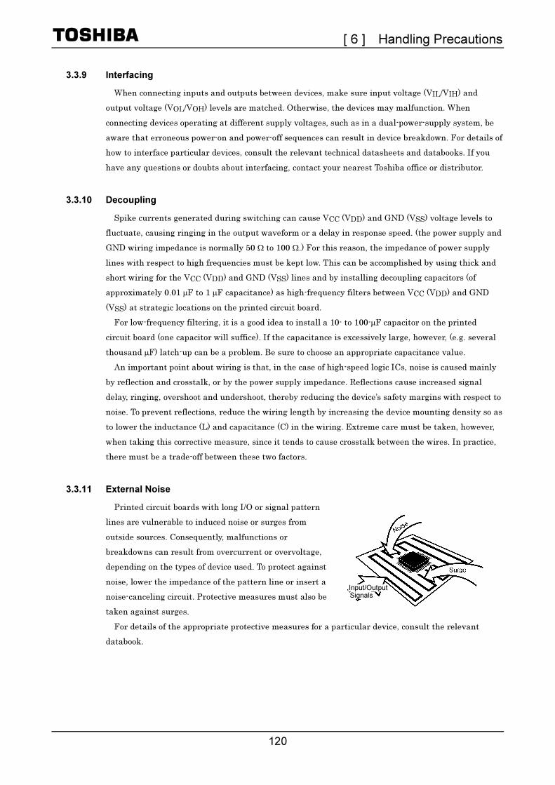
[ 6 ] Handling Precautions
120
3.3.9 Interfacing
When connecting inputs and outputs between devices, make sure input voltage (VIL/VIH) and
output voltage (VOL/VOH) levels are matched. Otherwise, the devices may malfunction. When
connecting devices operating at different supply voltages, such as in a dual-power-supply system, be
aware that erroneous power-on and power-off sequences can result in device breakdown. For details of
how to interface particular devices, consult the relevant technical datasheets and databooks. If you
have any questions or doubts about interfacing, contact your nearest Toshiba office or distributor.
3.3.10 Decoupling
Spike currents generated during switching can cause VCC (VDD) and GND (VSS) voltage levels to
fluctuate, causing ringing in the output waveform or a delay in response speed. (the power supply and
GND wiring impedance is normally 50 Ω to 100 Ω.) For this reason, the impedance of power supply
lines with respect to high frequencies must be kept low. This can be accomplished by using thick and
short wiring for the VCC (VDD) and GND (VSS) lines and by installing decoupling capacitors (of
approximately 0.01 µF to 1 µF capacitance) as high-frequency filters between VCC (VDD) and GND
(VSS) at strategic locations on the printed circuit board.
For low-frequency filtering, it is a good idea to install a 10- to 100-µF capacitor on the printed
circuit board (one capacitor will suffice). If the capacitance is excessively large, however, (e.g. several
thousand µF) latch-up can be a problem. Be sure to choose an appropriate capacitance value.
An important point about wiring is that, in the case of high-speed logic ICs, noise is caused mainly
by reflection and crosstalk, or by the power supply impedance. Reflections cause increased signal
delay, ringing, overshoot and undershoot, thereby reducing the device’s safety margins with respect to
noise. To prevent reflections, reduce the wiring length by increasing the device mounting density so as
to lower the inductance (L) and capacitance (C) in the wiring. Extreme care must be taken, however,
when taking this corrective measure, since it tends to cause crosstalk between the wires. In practice,
there must be a trade-off between these two factors.
3.3.11 External Noise
Printed circuit boards with long I/O or signal pattern
lines are vulnerable to induced noise or surges from
outside sources. Consequently, malfunctions or
breakdowns can result from overcurrent or overvoltage,
depending on the types of device used. To protect against
noise, lower the impedance of the pattern line or insert a
noise-canceling circuit. Protective measures must also be
taken against surges.
For details of the appropriate protective measures for a particular device, consult the relevant
databook.
Input/OutputSignals

[ 6 ] Handling Precautions
121
3.3.12 Electromagnetic Interference
Widespread use of electrical and electronic equipment in recent years has brought with it radio and
TV reception problems due to electromagnetic interference. To use the radio spectrum effectively and
to maintain radio communications quality, each country has formulated regulations limiting the
amount of electromagnetic interference which can be generated by individual products.
Electromagnetic interference includes conduction noise propagated through power supply and
telephone lines, and noise from direct electromagnetic waves radiated by equipment. Different
measurement methods and corrective measures are used to assess and counteract each specific type
of noise.
Difficulties in controlling electromagnetic interference derive from the fact that there is no method
available which allows designers to calculate, at the design stage, the strength of the electromagnetic
waves which will emanate from each component in a piece of equipment. For this reason, it is only
after the prototype equipment has been completed that the designer can take measurements using a
dedicated instrument to determine the strength of electromagnetic interference waves. Yet it is
possible during system design to incorporate some measures for the prevention of electromagnetic
interference, which can facilitate taking corrective measures once the design has been completed.
These include installing shields and noise filters, and increasing the thickness of the power supply
wiring patterns on the printed circuit board. One effective method, for example, is to devise several
shielding options during design, and then select the most suitable shielding method based on the
results of measurements taken after the prototype has been completed.
3.3.13 Peripheral Circuits
In most cases semiconductor devices are used with peripheral circuits and components. The input
and output signal voltages and currents in these circuits must be chosen to match the semiconductor
device’s specifications. The following factors must be taken into account.
(1) Inappropriate voltages or currents applied to a device’s input pins may cause it to operate
erratically. Some devices contain pull-up or pull-down resistors. When designing your system,
remember to take the effect of this on the voltage and current levels into account.
(2) The output pins on a device have a predetermined external circuit drive capability. If this drive
capability is greater than that required, either incorporate a compensating circuit into your
design or carefully select suitable components for use in external circuits.
3.3.14 Safety Standards
Each country has safety standards which must be observed. These safety standards include
requirements for quality assurance systems and design of device insulation. Such requirements must
be fully taken into account to ensure that your design conforms to the applicable safety standards.

[ 6 ] Handling Precautions
122
3.3.15 Other Precautions
(1) When designing a system, be sure to incorporate fail-safe and other appropriate measures
according to the intended purpose of your system. Also, be sure to debug your system under
actual board-mounted conditions.
(2) If a plastic-package device is placed in a strong electric field, surface leakage may occur due to
the charge-up phenomenon, resulting in device malfunction. In such cases take appropriate
measures to prevent this problem, for example by protecting the package surface with a
conductive shield.
(3) With some microcomputers and MOS memory devices, caution is required when powering on or
resetting the device. To ensure that your design does not violate device specifications, consult the
relevant databook for each constituent device.
(4) Ensure that no conductive material or object (such as a metal pin) can drop onto and short the
leads of a device mounted on a printed circuit board.
3.4 Inspection, Testing and Evaluation
3.4.1 Grounding
Ground all measuring instruments, jigs, tools and soldering irons to
earth.
Electrical leakage may cause a device to break down or may result in
electric shock.
3.4.2 Inspection Sequence
1) Do not insert devices in the wrong orientation. Make sure that the
positive and negative electrodes of the power supply are correctly
connected. Otherwise, the rated maximum current or maximum
power dissipation may be exc0eeded and the device may break down
or undergo performance degradation, causing it to catch fire or
explode, resulting in injury to the user.
2) When conducting any kind of evaluation, inspection or testing using
AC power with a peak voltage of 42.4 V or DC power exceeding 60 V,
be sure to connect the electrodes or probes of the testing equipment
to the device under test before powering it on. Connecting the
electrodes or probes of testing equipment to a device while it is
powered on may result in electric shock, causing injury.
(1) Apply voltage to the test jig only after inserting the device securely into it. When applying or
removing power, observe the relevant precautions, if any.
(2) Make sure that the voltage applied to the device is off before removing the device from the test
jig. Otherwise, the device may undergo performance degradation or be destroyed.
(3) Make sure that no surge voltages from the measuring equipment are applied to the device.

[ 6 ] Handling Precautions
123
(4) The chips housed in tape carrier packages (TCPs) are bare chips and are therefore exposed.
During inspection take care not to crack the chip or cause any flaws in it.
Electrical contact may also cause a chip to become faulty. Therefore make sure that nothing
comes into electrical contact with the chip.
3.5 Mounting
There are essentially two main types of semiconductor device package: lead insertion and surface
mount. During mounting on printed circuit boards, devices can become contaminated by flux or
damaged by thermal stress from the soldering process. With surface-mount devices in particular, the
most significant problem is thermal stress from solder reflow, when the entire package is subjected to
heat. This section describes a recommended temperature profile for each mounting method, as well as
general precautions which you should take when mounting devices on printed circuit boards. Note,
however, that even for devices with the same package type, the appropriate mounting method varies
according to the size of the chip and the size and shape of the lead frame. Therefore, please consult
the relevant technical datasheet and databook.
3.5.1 Lead Forming
1) Always wear protective glasses when cutting the leads of a device
with clippers or a similar tool. If you do not, small bits of metal flying
off the cut ends may damage your eyes.
2) Do not touch the tips of device leads. Because some types of device
have leads with pointed tips, you oay prick your finger.
Semiconductor devices must undergo a process in which the leads are cut and formed before the
devices can be mounted on a printed circuit board. If undue stress is applied to the interior of a device
during this process, mechanical breakdown or performance degradation can result. This is
attributable primarily to differences between the stress on the device’s external leads and the stress
on the internal leads. If the relative difference is great enough, the device’s internal leads, adhesive
properties or sealant can be damaged. Observe these precautions during the lead-forming process
(this does not apply to surface-mount devices):
(1) Lead insertion hole intervals on the printed circuit board should match the lead pitch of the
device precisely.
(2) If lead insertion hole intervals on the printed circuit board do not precisely match the lead pitch
of the device, do not attempt to forcibly insert devices by pressing on them or by pulling on their
leads.
(3) For the minimum clearance specification between a device and a
printed circuit board, refer to the relevant device’s datasheet and
databook. If necessary, achieve the required clearance by forming
the device’s leads appropriately. Do not use the spacers which are
used to raise devices above the surface of the printed circuit board
during soldering to achieve clearance. These spacers normally
continue to expand due to heat, even after the solder has begun to solidify; this applies severe
stress to the device.

[ 6 ] Handling Precautions
124
(4) Observe the following precautions when forming the leads of a device prior to mounting.
Use a tool or jig to secure the lead at its base (where the lead meets the device package)
while bending so as to avoid mechanical stress to the device. Also avoid bending or stretching
device leads repeatedly.
Be careful not to damage the lead during lead forming.
Follow any other precautions described in the individual datasheets and databooks for each
device and package type.
3.5.2 Mounting on Printed Circuit Board
When soldering the leads on the printed circuit board, be careful not to leave stress on the leads.
Leads must be shaped and aligned to the hole size, and space must be left between the device and
the board (Figure 3.6). If leads are not shaped but forced into holes or stress is applied by a tool,
corrosion or whiskers may occur where stress is applied, resulting in cutout or shorting of leads. Thus,
hole size must be aligned to the lead interval.
Figure 3.3 How to Bend Leads Figure 3.4 How to Bend Leads Using Metal Mold
Figure 3.5 How to Bend Leads
Device body Lead
5 mm or longer
Device
Leave enough space so that
even if the bending mold pulls
the lead, the device does not
touch the lead holding mold.Leave space
Leave holding mold
3 mm or longer
3 mm or longer
30° or less 30° or less
30° or less
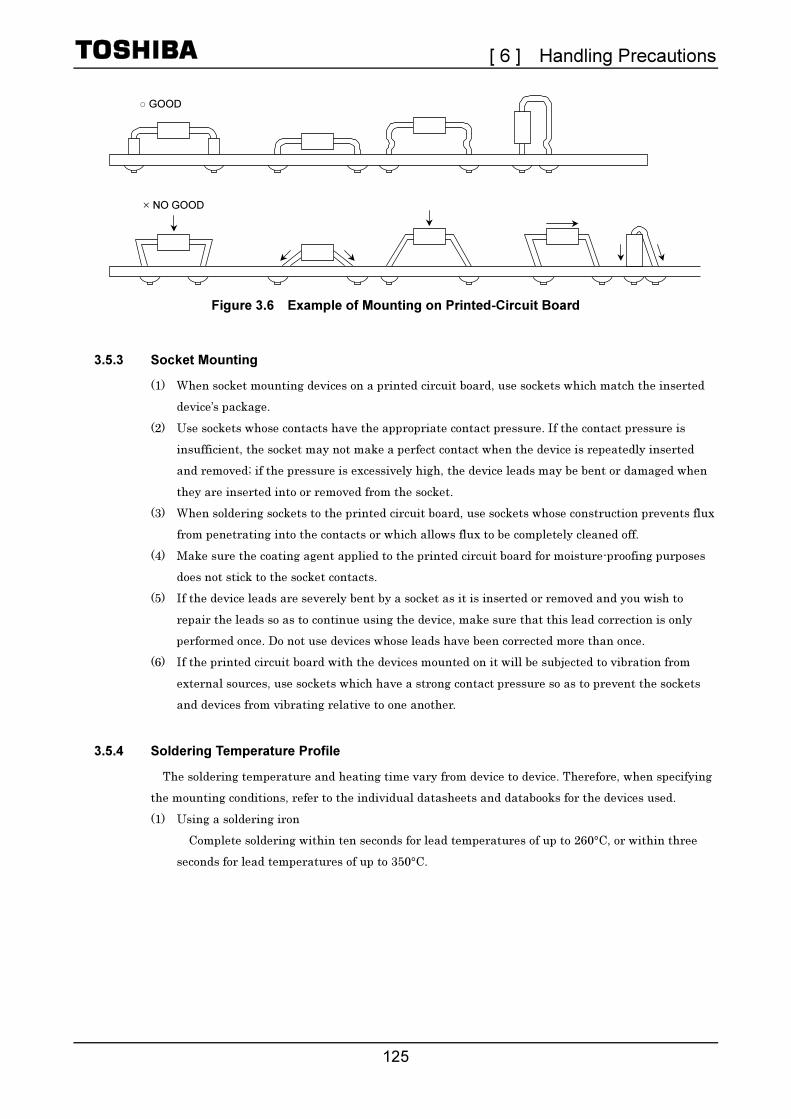
[ 6 ] Handling Precautions
125
Figure 3.6 Example of Mounting on Printed-Circuit Board
3.5.3 Socket Mounting
(1) When socket mounting devices on a printed circuit board, use sockets which match the inserted
device’s package.
(2) Use sockets whose contacts have the appropriate contact pressure. If the contact pressure is
insufficient, the socket may not make a perfect contact when the device is repeatedly inserted
and removed; if the pressure is excessively high, the device leads may be bent or damaged when
they are inserted into or removed from the socket.
(3) When soldering sockets to the printed circuit board, use sockets whose construction prevents flux
from penetrating into the contacts or which allows flux to be completely cleaned off.
(4) Make sure the coating agent applied to the printed circuit board for moisture-proofing purposes
does not stick to the socket contacts.
(5) If the device leads are severely bent by a socket as it is inserted or removed and you wish to
repair the leads so as to continue using the device, make sure that this lead correction is only
performed once. Do not use devices whose leads have been corrected more than once.
(6) If the printed circuit board with the devices mounted on it will be subjected to vibration from
external sources, use sockets which have a strong contact pressure so as to prevent the sockets
and devices from vibrating relative to one another.
3.5.4 Soldering Temperature Profile
The soldering temperature and heating time vary from device to device. Therefore, when specifying
the mounting conditions, refer to the individual datasheets and databooks for the devices used.
(1) Using a soldering iron
Complete soldering within ten seconds for lead temperatures of up to 260°C, or within three
seconds for lead temperatures of up to 350°C.
GOOD
× NO GOOD
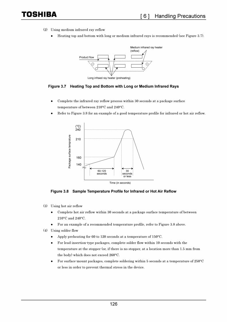
[ 6 ] Handling Precautions
126
(2) Using medium infrared ray reflow
Heating top and bottom with long or medium infrared rays is recommended (see Figure 3.7).
Figure 3.7 Heating Top and Bottom with Long or Medium Infrared Rays
Complete the infrared ray reflow process within 30 seconds at a package surface
temperature of between 210°C and 240°C.
Refer to Figure 3.8 for an example of a good temperature profile for infrared or hot air reflow.
Figure 3.8 Sample Temperature Profile for Infrared or Hot Air Reflow
(3) Using hot air reflow
Complete hot air reflow within 30 seconds at a package surface temperature of between
210°C and 240°C.
For an example of a recommended temperature profile, refer to Figure 3.8 above.
(4) Using solder flow
Apply preheating for 60 to 120 seconds at a temperature of 150°C.
For lead insertion-type packages, complete solder flow within 10 seconds with the
temperature at the stopper (or, if there is no stopper, at a location more than 1.5 mm from
the body) which does not exceed 260°C.
For surface-mount packages, complete soldering within 5 seconds at a temperature of 250°C
or less in order to prevent thermal stress in the device.
Medium infrared ray heater
(reflow)
Long infraed ray heater (preheating)
Product flow
210
30secondsor less
Time (in seconds)
60-120seconds
(°C) 240
160
140
Packa
ge s
urf
ace
te
mp
ratu
re

[ 6 ] Handling Precautions
127
Figure 3.9 shows an example of a recommended temperature profile for surface-mount
packages using solder flow.
Figure 3.9 Sample Temperature Profile for Solder Flow
3.5.5 Flux Cleaning and Ultrasonic Cleaning
(1) When cleaning circuit boards to remove flux, make sure that no residual reactive ions such as Na
or Cl remain. Note that organic solvents react with water to generate hydrogen chloride and
other corrosive gases which can degrade device performance.
(2) Washing devices with water will not cause any problems. However, make sure that no reactive
ions such as sodium and chlorine are left as a residue. Also, be sure to dry devices sufficiently
after washing.
(3) Do not rub device markings with a brush or with your hand during cleaning or while the devices
are still wet from the cleaning agent. Doing so can rub off the markings.
(4) The dip cleaning, shower cleaning and steam cleaning processes all involve the chemical action of
a solvent. Use only recommended solvents for these cleaning methods. When immersing devices
in a solvent or steam bath, make sure that the temperature of the liquid is 50°C or below, and
that the circuit board is removed from the bath within one minute.
(5) Ultrasonic cleaning should not be used with hermetically-sealed ceramic packages such as a
leadless chip carrier (LCC), pin grid array (PGA) or charge-coupled device (CCD), because the
bonding wires can become disconnected due to resonance during the cleaning process. Even if a
device package allows ultrasonic cleaning, limit the duration of ultrasonic cleaning to as short a
time as possible, since long hours of ultrasonic cleaning degrade the adhesion between the mold
resin and the frame material. The following ultrasonic cleaning conditions are recommended:
Frequency: 27 kHz to 29 kHz
Ultrasonic output power: 300 W or less (0.25 W/cm2 or less)
Cleaning time: 30 seconds or less
Suspend the circuit board in the solvent bath during ultrasonic cleaning in such a way that the
ultrasonic vibrator does not come into direct contact with the circuit board or the device.
Time (in seconds)
60-120 seconds
(°C) 250
160
140
Packa
ge s
urf
ace
te
mp
ratu
re
5 secondsor less

[ 6 ] Handling Precautions
128
3.5.6 No Cleaning
If analog devices or high-speed devices are used without being cleaned, flux residues may cause
minute amounts of leakage between pins. Similarly, dew condensation, which occurs in environments
containing residual chlorine when power to the device is on, may cause between-lead leakage or
migration. Therefore, Toshiba recommends that these devices be cleaned.
However, if the flux used contains only a small amount of halogen (0.05 W% or less), the devices
may be used without cleaning without any problems.
3.5.7 Mounting Tape Carrier Packages (TCPs)
(1) When tape carrier packages (TCPs) are mounted, measures must be taken to prevent
electrostatic breakdown of the devices.
(2) If devices are being picked up from tape, or outer lead bonding (OLB) mounting is being carried
out, consult the manufacturer of the insertion machine which is being used, in order to establish
the optimum mounting conditions in advance and to avoid any possible hazards.
(3) The base film, which is made of polyimide, is hard and thin. Be careful not to cut or scratch your
hands or any objects while handling the tape.
(4) When punching tape, try not to scatter broken pieces of tape too much.
(5) Treat the extra film, reels and spacers left after punching as industrial waste, taking care not to
destroy or pollute the environment.
(6) Chips housed in tape carrier packages (TCPs) are bare chips and therefore have their reverse
side exposed. To ensure that the chip will not be cracked during mounting, ensure that no
mechanical shock is applied to the reverse side of the chip. Electrical contact may also cause a
chip to fail. Therefore, when mounting devices, make sure that nothing comes into electrical
contact with the reverse side of the chip.
If your design requires connecting the reverse side of the chip to the circuit board, please consult
Toshiba or a Toshiba distributor beforehand.
3.5.8 Mounting Chips
Devices delivered in chip form tend to degrade or break under external forces much more easily
than plastic-packaged devices. Therefore, caution is required when handling this type of device.
(1) Mount devices in a properly prepared environment so that chip surfaces will not be exposed to
polluted ambient air or other polluted substances.
(2) When handling chips, be careful not to expose them to static electricity.
In particular, measures must be taken to prevent static damage during the mounting of chips.
With this in mind, Toshiba recommend mounting all peripheral parts first and then mounting
chips last (after all other components have been mounted).
(3) Make sure that PCBs (or any other kind of circuit board) on which chips are being mounted do
not have any chemical residues on them (such as the chemicals which were used for etching the
PCBs).
(4) When mounting chips on a board, use the method of assembly that is most suitable for
maintaining the appropriate electrical, thermal and mechanical properties of the semiconductor
devices used.
*: For details of devices in chip form, refer to the relevant device’s individual datasheets.

[ 6 ] Handling Precautions
129
3.5.9 Circuit Board Coating
When devices are to be used in equipment requiring a high degree of reliability or in extreme
environments (where moisture, corrosive gas or dust is present), circuit boards may be coated for
protection. However, before doing so, you must carefully consider the possible stress and
contamination effects that may result and then choose the coating resin which results in the
minimum level of stress to the device.
3.5.10 Heat Sinks
(1) When attaching a heat sink to a device, be careful not to apply excessive force to the device in the
process.
(2) When attaching a device to a heat sink by fixing it at two or more locations, evenly tighten all the
screws in stages (i.e. do not fully tighten one screw while the rest are still only loosely tightened).
Finally, fully tighten all the screws up to the specified torque.
(3) Drill holes for screws in the heat sink exactly as specified. Smooth
the surface by removing burrs and protrusions or indentations
which might interfere with the installation of any part of the
device.
(4) A coating of silicone compound can be applied between the heat
sink and the device to improve heat conductivity. Be sure to apply
the coating thinly and evenly; do not use too much. Also, be sure to
use a non-volatile compound, as volatile compounds can crack after a time, causing the heat
radiation properties of the heat sink to deteriorate.
(5) If the device is housed in a plastic package, use caution when selecting the type of silicone
compound to be applied between the heat sink and the device. With some types, the base oil
separates and penetrates the plastic package, significantly reducing the useful life of the device.
Two recommended silicone compounds in which base oil separation is not a problem are YG6260
from Toshiba Silicone.
(6) Heat-sink-equipped devices can become very hot during operation. Do not touch them, or you
may sustain a burn.
3.5.11 Tightening Torque
(1) Make sure the screws are tightened with fastening torques not exceeding the torque values
stipulated in individual datasheets and databooks for the devices used.
(2) Do not allow a power screwdriver (electrical or air-driven) to touch devices.
[ 6 ] Handling Precautions
130
3.5.12 Repeated Device Mounting and Usage
Do not remount or re-use devices which fall into the categories listed below; these devices may
cause significant problems relating to performance and reliability.
(1) Devices which have been removed from the board after soldering
(2) Devices which have been inserted in the wrong orientation or which have had reverse current
applied
(3) Devices which have undergone lead forming more than once
3.6 Protecting Devices in the Field
3.6.1 Temperature
Semiconductor devices are generally more sensitive to temperature than are other electronic
components. The various electrical characteristics of a semiconductor device are dependent on the
ambient temperature at which the device is used. It is therefore necessary to understand the
temperature characteristics of a device and to incorporate device derating into circuit design. Note
also that if a device is used above its maximum temperature rating, device deterioration is more rapid
and it will reach the end of its usable life sooner than expected.
3.6.2 Humidity
Resin-molded devices are sometimes improperly sealed. When these devices are used for an
extended period of time in a high-humidity environment, moisture can penetrate into the device and
cause chip degradation or malfunction. Furthermore, when devices are mounted on a regular printed
circuit board, the impedance between wiring components can decrease under high-humidity
conditions. In systems which require a high signal-source impedance, circuit board leakage or leakage
between device lead pins can cause malfunctions. The application of a moisture-proof treatment to the
device surface should be considered in this case. On the other hand, operation under low-humidity
conditions can damage a device due to the occurrence of electrostatic discharge. Unless damp-proofing
measures have been specifically taken, use devices only in environments with appropriate ambient
moisture levels (i.e. within a relative humidity range of 40% to 60%).
3.6.3 Corrosive Gases
Corrosive gases can cause chemical reactions in devices, degrading device characteristics.
For example, sulphur-bearing corrosive gases emanating from rubber placed near a device
(accompanied by condensation under high-humidity conditions) can corrode a device’s leads. The
resulting chemical reaction between leads forms foreign particles which can cause electrical leakage.

[ 6 ] Handling Precautions
131
3.6.4 Radioactive and Cosmic Rays
Most industrial and consumer semiconductor devices are not designed with protection against
radioactive and cosmic rays. Devices used in aerospace equipment or in radioactive environments
must therefore be shielded.
3.6.5 Strong Electrical and Magnetic Fields
Devices exposed to strong magnetic fields can undergo a polarization phenomenon in their
plastic material, or within the chip, which gives rise to abnormal symptoms such as impedance
changes or increased leakage current. Failures have been reported in LSIs mounted near
malfunctioning deflection yokes in TV sets. In such cases the device’s installation location must be
changed or the device must be shielded against the electrical or magnetic field. Shielding against
magnetism is especially necessary for devices used in an alternating magnetic field because of the
electromotive forces generated in this type of environment.
3.6.6 Interference from Light
(ultraviolet rays, sunlight, fluorescent lamps and incandescent lamps)
Light striking a semiconductor device generates electromotive force due to photoelectric effects. In
some cases the device can malfunction. This is especially true for devices in which the internal chip is
exposed. When designing circuits, make sure that devices are protected against incident light from
external sources. This problem is not limited to optical semiconductors and EPROMs. All types of
device can be affected by light.
3.6.7 Dust and Oil
Just like corrosive gases, dust and oil can cause chemical reactions in devices, which will adversely
affect a device’s electrical characteristics. To avoid this problem, do not use devices in dusty or oily
environments. This is especially important for optical devices because dust and oil can affect a
device’s optical characteristics as well as its physical integrity and the electrical performance factors
mentioned above.
3.6.8 Fire
Semiconductor devices are combustible; they can emit smoke and catch fire if heated sufficiently.
When this happens, some devices may generate poisonous gases. Devices should therefore never be
used in close proximity to an open flame or a heat-generating body, or near flammable or combustible
materials.
3.7 Disposal of Devices and Packing Materials
When discarding unused devices and packing materials, follow all procedures specified by local
regulations in order to protect the environment against contamination.

[ 6 ] Handling Precautions
132
4. Precautions and Usage Considerations Specific to Each Product Group
This section describes matters specific to each product group which need to be taken into
consideration when using devices.
4.1 Bipolar Ics
4.1.1 ICs for Use in Automobiles
(1) Design
1) If your design includes an inductive load such as a motor coil,
incorporate diodes into your design to prevent negative current
from flowing in. Otherwise the device may malfunction or break
down due to rush currents or counter electromotive force
generated when the device is powered on and off. For
information on how to connect the diodes, refer to the relevant
individual datasheets for automobile ICs. Breakdown of the
devices may result in injury.
2) Ensure that the power supply to any device which incorporates
protective functions is stable. If the power supply is unstable,
the device may operate erratically, preventing the protective
functions from working correctly.
If protective functions fail, the device may break down, causing
the device to explode and resulting in injury to the user.
Heat radiation
System power supply and driver ICs generate heat. When using these devices, refer to the
technical databooks entitled Bipolar ICs for Use in Automobiles and General-Purpose
Bipolar IC Databook, and incorporate sufficient heat radiation for the devices used into your
design, so that the heat generated will not exceed the stipulated junction temperature (Tj) at
which the ICs’ internal heat-isolating protective circuits are activated.
Power supply fuses
These ICs contain various protective circuits to prevent them from breaking down due to
faulty wiring or when pulses of noise are input to the power supply. However, should the IC
break down, a large current may continue to flow. To prevent this, use a fuse of the
appropriate capacity for the power supply.
For information about the various types of protective circuit incorporated into the ICs, refer
to the individual datasheets for the devices used.
Power supply
Do not abruptly increase or decrease the power supply to a device.

[ 6 ] Handling Precautions
133
(2) Mounting
Heat sinks
Depending on the type of package used (e.g. an HSIP7-P-2.54), a device’s characteristics
may be degraded if the package is attached to a heat sink using screws. In such cases please
consult Toshiba or a Toshiba distributor.
4.1.2 Communication Equipment ICs
(1) Design
When using these devices in power amps or system power supplies, be aware that since the
effective current capacity of the output pins is 100 mA or higher, a device’s DC output current
may increase if there is any problem caused by an external component (in particular, leak
current from a feedback resistor or a negative feedback capacitor). In some cases this will cause
the product to generate heat or to catch fire. Take this into account when designing your product
and choosing which components to use. For more detailed information, please refer to the
individual datasheets or databooks.
(2) Mounting
Trends toward lightweight and compact design in mobile communications have resulted in the
device-mounting board becoming vulnerable to distortion or deformation due to a lack of strength.
This causes the devices to be imperfectly connected when mounted on the board. Therefore,
carefully examine the board design and mounting methods to ensure that device pins are firmly
connected to the board.
4.1.3 Audio/Video Equipment ICs
These devices are designed for use in consumer electronics, typically in television and audio
equipment. When using these devices in low-frequency audio amps, system power supply ICs, driver
ICs or power ICs, pay attention to the following points:
(1) Design
Circuit design
Large leakage current in input or negative feedback capacitors causes the DC output
voltage of power ICs to increase. In this case, if the speaker’s DC input withstand voltage is
low, the speaker may emit smoke or catch fire.
This must be fully taken into account when selecting the types of capacitor and speaker to
use, especially in the case of power ICs of the BTL (bridge-tied load) connection type, in
which the DC output voltage is input directly to the speaker.
Heat radiation
Power ICs, system power supply ICs and driver ICs generate heat. When using these
devices, and incorporate sufficient heat radiation for the devices used into your design, so
that the heat generated will not exceed the stipulated junction temperature (Tj = 150°C) at
which the ICs’ internal thermal shutdown protective circuits are activated. For more detailed
information, refer to the individual product datasheets and to the general audio/car audio
LSI databooks.
Also, take into account the operating temperature ranges and characteristics of the
peripheral components used with power ICs.

[ 6 ] Handling Precautions
134
Power supply fuses
These ICs contain various protective circuits to prevent them from breaking down due to
faulty wiring or noise pulses on the power supply input. However, should the IC break down,
a large current may continue to flow. To prevent this, use a fuse of the appropriate capacity
for the power supply.
4.1.4 ICs for Motors
(1) Design
When designing a circuit incorporating a motor, be sure to incorporate a diode to act as a
current-limiting resistance and to absorb any counter electromotive force so that the starting
current or counter electromotive force does not cause any malfunction or breakdown in the
IC. For detailed information concerning this type of design, refer to the relevant individual
datasheets or databooks for ICs for motors.
Circuits which are used to protect ICs from excessive current do not always work. If an IC is
used outside its absolute maximum ratings, the IC may break down before the protective
circuit is activated.
Be sure to use a stable power supply for the IC. If the power supply is unstable, the internal
circuits of the IC may function erratically, possibly causing the IC to break down.
(2) Heat radiation
When using a driver IC, be sure to incorporate heat radiation so that the junction
temperature (Tj) will never exceed 150°C. Since ICs generate considerable heat, ICs may
break down if adequate heat radiation is not provided.
Circuits which are used to protect devices from excessive heat do not always work. If an IC is
used outside its absolute maximum ratings, it may break down before the protective circuit
is activated.
When attaching a heat sink to the driver IC, avoid excessive mechanical stress. Also note
that some ICs inhibit the action of silicone rubber.
When incorporating heat radiation or attaching heat sinks, refer to the relevant individual
datasheets or databooks for ICs for motors.
(3) Power supply fuses
In order to prevent excessive current from flowing continuously when the IC breaks down, use
a power supply fuse of an appropriate capacity. An IC may break down when used outside its
absolute maximum ratings, or when wires or loads induce unusual pulse noise. The fuse capacity
must be carefully determined in order to minimize any negative effect in the case of an IC
breakdown and the resulting large current flow.

[ 6 ] Handling Precautions
135
4.1.5 Cautions about Power Dissipation (Constant State)
A transistor by itself will often differ from a board- mounted transistor in its power dissipation
characteristics. Changes in power dissipation for representative package types, due to board
mounting, are described below.
Each representative package type and the power dissipation change is explained below.
4.1.5.1 Super-Mini Transistors
Allowable power dissipation of a super-
mini transistor is 100 to 150 mW as a
single unit.
However, when it is mounted on a
ceramic board, this value increases
depending on the board size. this is
shown in Figure 4.1 (transistors used:
2SA1162 and 2SC2712).
4.1.5.2 Power-Mini Transistors
Since power-mini transistors are of
compact size, Pcmax is only 500 mW;
however, when they are mounted on a
circuit board, thermal diffusion from a
drain fin to the board will be high. The
drain power dissipation will then range
from 1.0 W to 2.0 W, and a circuit design
capability equivalent to that of the TO-
92MOD (800 to 900 mW) or TO-126 (1.0
to 1.2 W) is possible. Figure 4.2 shows the
drain power dissipation for a typical case
of circuit-board mounting of a 2SC2873 or
2SA1213.
4.1.5.3 Power-Mold Transistors
For straight-type power-mold
transistors, the power dissipation (Pc) = 1
W However, when LB-type transistors
have a drain-fin, their installed power
dissipation increases significantly. When a
power-mold transistor is soldered to an
alumina-ceramic board, Pc (1) (1,000
mm2) = 2 W, Pc (2) (2,500 mm2) = 3 W Figure 4.3 show the relationship between drain power
dissipation Pc and ambient temperature Ta for the transistors 2SC3074 and 2SA1244.
Figure 4.1 Pc (max) when Mounted on Alumi-
Ceramic Board
Ta Characteristic (2SA1162, 2SC2712)
Figure 4.2 Pc (max) when Mounted on Alumi-
Ceramic Board
Ta Characteristic (2SC2873, 2SA1213)
Ambient temperature Ta (°C)
Pow
er
dis
sip
ation P
c (m
W)
Condition:
Quantity on PC board
1 pc, without protectant
coating reflow
soldering.
500
0−20 0 20 40 60 80 100 120 140
100
200
300
400
20 × 15 × 0.8
20 × 30 × 0.8
40 × 50 × 0.8 mmt
Without PC board
Ambient temperature Ta (°C)
Pow
er
dis
sip
ation P
c (m
W)
2.0
0
1.0
−20 0 20 40 60 80 100 120 140 160
Condition:
Quantity on PC board
1 pc, reflow soldering.
40 × 50 × 0.8 mmt
20 × 30 × 0.8
Without PC board
15 × 15 × 0.8

[ 6 ] Handling Precautions
136
Figure 4.3 Power Dissipation Pc and Ambient Temperature Ta when
Transistors are Mounted on Alumina-Ceramic Boards
(for 2SC3074 and 2SA1244 devices)
Ambient temperature Ta (°C)
Pow
er
dis
sip
ation P
c (m
W)
3
00
4
1
2
20 40 60 80 100 120 140
Quantity on PC board 1 pc,
mounted on ceramic board,
Ta = 25°C
160
50 × 50 × 0.8 mmt
30 × 30 × 0.8
Without PC board

[ 8 ] Package Dimensions


[ 8 ] Package Dimensions
247
[ 8 ] Package Dimensions
Unit: mm
fSC sESC TESC
0.8
± 0.
050.
10.
1
1.0
± 0.
05
0.52 ± 0.03
0.48 + 0.02
– 0.03
0.6 ± 0.05
0.2 ± 0.050.1 ± 0.05
Cat
hode
Mar
k
0.07 M A
A
1.0
± 0.
050.
20.
2
1.4
± 0.
1
0.52 ± 0.03
0.6 ± 0.05
0.2 ± 0.05 0.12 ± 0.05
Cat
hode
Mar
k
1.2
± 0
.10.
20.
2
1.6
± 0
.1
0.55 ± 0.05
0.8 ± 0.1
0.3 ± 0.05 0.13 ± 0.05
Cat
hode
Mar
k
ESC USC fSM
1.25 + 0.2 – 0.1
0.15 + 0.1 – 0.060.3 + 0.1 – 0.05
Cat
hode
Mar
k
1.7
0.15
+ 0
.2 –
0.1
0.9
+ 0
.2 –
0.1
2.5
± 0
.2
0 ± 0.05
TESM SSM USM
2.1 ± 0.1
1.25 ± 0.1
2.0
± 0
.2
0.90
± 0
.11.
3 ±
0.1
0.65
0.65 3
1
2
0.3 +
0.1
– 0
0.15
0 –
0.1
0.7
+ 0
.1 –
0.0
5

[ 8 ] Package Dimensions
248
Unit: mm
S-MINI PW-X PW-MINI
TESQ USQ SMQ (ESOP4-P-1.90)
1.2 ± 0.05
0.9 ± 0.05
1.2
± 0
.05
0.52
± 0
.05
0.8
± 0
.05 1
2
4
3 0.2
± 0
.05
0.12
± 0
.05
2.1 ± 0.1
1.25 ± 0.1
2.0
± 0
.2
1.3
± 0
.1 1
2
4
3
0 –
0.1
0.7
0.95
+ 0
.05
– 0
.15
0.2 +
0.1
– 0
.05
0.15
± 0
.05
2.9
± 0
.2
0.05
± 0
.05
1.90
0.6
0.4
0.8
0.3
2.9 + 0.2 – 0.3
1
2
5
5
4
0.850.55
3
0.16
+ 0
.1 –
0.0
6
1.1 +
0.1
5 –
0.0
5
1.50 + 0.25 – 0.15
ESV (SON5-P-0.50) USV (SSOP5-P-0.65) SMV (SSOP5-P-0.95)
1.6 ± 0.05
1.6
± 0
.05
0.5
0.55
± 0
.05
0.5
0.2
± 0
.05
0.12
± 0
.05
3
2
15
4
1.2 ± 0.05
2.1 ± 0.1
2.0
± 0
.2
1.3
± 0
.1
1.25 ± 0.1
0.65
0.65
1 5
4
2
3
0.2
+ 0
.1 –
0.0
5
0 ~ 0.1
0.15
0.9
± 0
.1 + 0
.1 –
0.0
5
2.8 + 0.2- 0.3
1.6 + 0.2- 0.1
2.9
± 0
.2
1.9
± 0
.2
0.4
± 0
.1
0.95
0.95 1
2
3 4
5
1.1 +
0.2
– 0
.1
0 –
0.1
0.16
+ 0
.1 –
0.0
6
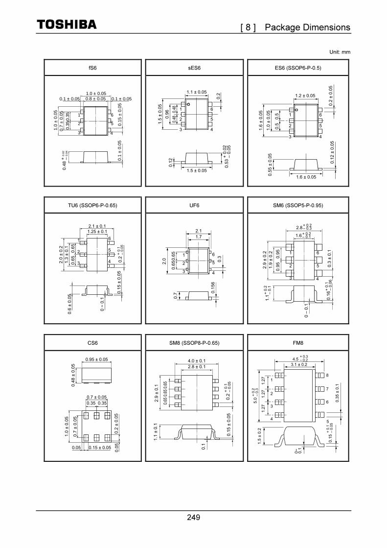
[ 8 ] Package Dimensions
249
Unit: mm
fS6 sES6 ES6 (SSOP6-P-0.5)
1.0 ± 0.050.1 ± 0.05 0.1 ± 0.050.8 ± 0.05
1.0
± 0
.05
0.7
± 0
.05
0.35
0.35 1
3
6
2 5
4
0.15
± 0
.05
0.1
± 0
.05
0.48
+ 0
.02
– 0.
04
TU6 (SSOP6-P-0.65) UF6 SM6 (SSOP5-P-0.95)
CS6 SM8 (SSOP8-P-0.65) FM8

[ 8 ] Package Dimensions
250
Unit: mm
SSOP20
HSOP20
CS20 5-53L 5-53P

[ 8 ] Package Dimensions
251
Unit: mm
5-53Q 5-23E 2-13B1A
2-13C1A 2-22C2A
S-AU84/S-AU85

[ 9 ] List of Final-Phase Products

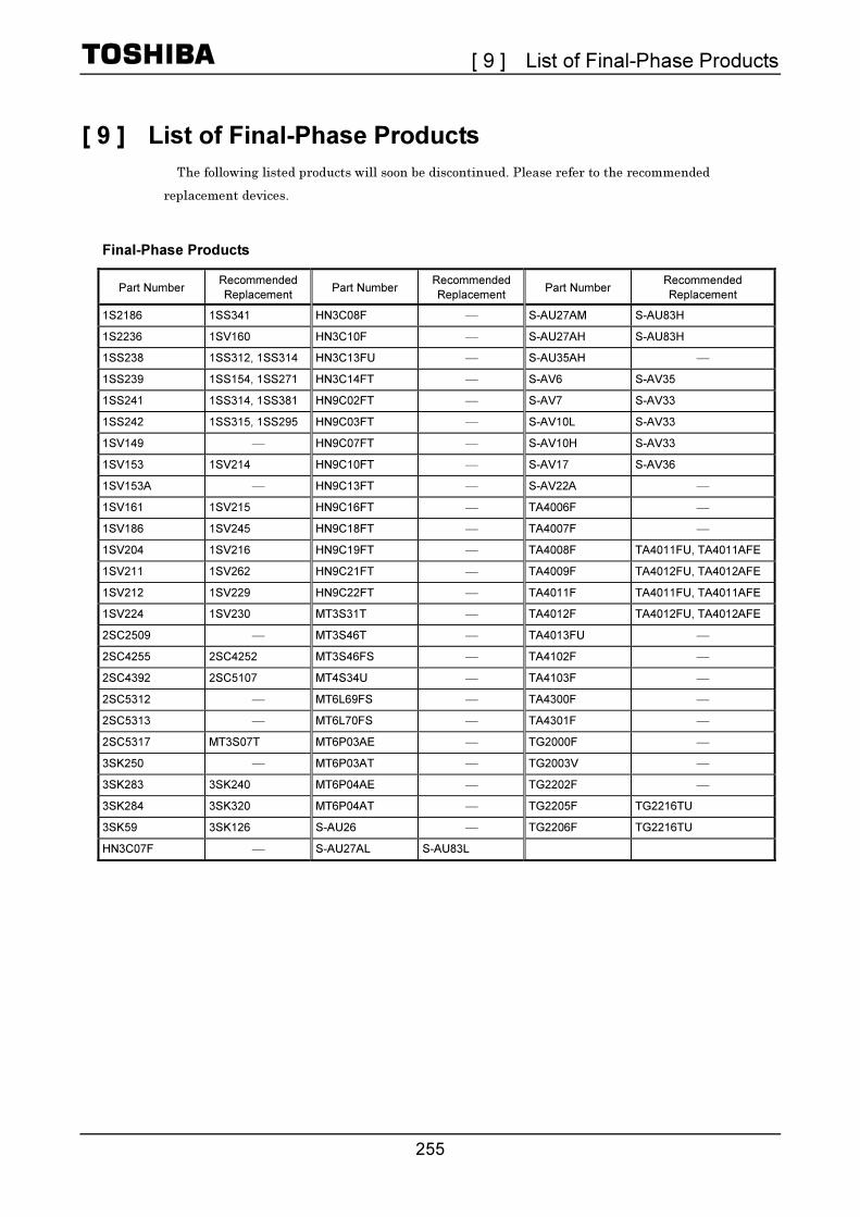
[ 9 ] List of Final-Phase Products
255
[ 9 ] List of Final-Phase Products
The following listed products will soon be discontinued. Please refer to the recommended
replacement devices.
Final-Phase Products
Part Number Recommended
Replacement Part Number
Recommended
Replacement Part Number
Recommended
Replacement
1S2186 1SS341 HN3C08F ⎯ S-AU27AM S-AU83H
1S2236 1SV160 HN3C10F ⎯ S-AU27AH S-AU83H
1SS238 1SS312, 1SS314 HN3C13FU ⎯ S-AU35AH ⎯
1SS239 1SS154, 1SS271 HN3C14FT ⎯ S-AV6 S-AV35
1SS241 1SS314, 1SS381 HN9C02FT ⎯ S-AV7 S-AV33
1SS242 1SS315, 1SS295 HN9C03FT ⎯ S-AV10L S-AV33
1SV149 ⎯ HN9C07FT ⎯ S-AV10H S-AV33
1SV153 1SV214 HN9C10FT ⎯ S-AV17 S-AV36
1SV153A ⎯ HN9C13FT ⎯ S-AV22A ⎯
1SV161 1SV215 HN9C16FT ⎯ TA4006F ⎯
1SV186 1SV245 HN9C18FT ⎯ TA4007F ⎯
1SV204 1SV216 HN9C19FT ⎯ TA4008F TA4011FU, TA4011AFE
1SV211 1SV262 HN9C21FT ⎯ TA4009F TA4012FU, TA4012AFE
1SV212 1SV229 HN9C22FT ⎯ TA4011F TA4011FU, TA4011AFE
1SV224 1SV230 MT3S31T ⎯ TA4012F TA4012FU, TA4012AFE
2SC2509 ⎯ MT3S46T ⎯ TA4013FU ⎯
2SC4255 2SC4252 MT3S46FS ⎯ TA4102F ⎯
2SC4392 2SC5107 MT4S34U ⎯ TA4103F ⎯
2SC5312 ⎯ MT6L69FS ⎯ TA4300F ⎯
2SC5313 ⎯ MT6L70FS ⎯ TA4301F ⎯
2SC5317 MT3S07T MT6P03AE ⎯ TG2000F ⎯
3SK250 ⎯ MT6P03AT ⎯ TG2003V ⎯
3SK283 3SK240 MT6P04AE ⎯ TG2202F ⎯
3SK284 3SK320 MT6P04AT ⎯ TG2205F TG2216TU
3SK59 3SK126 S-AU26 ⎯ TG2206F TG2216TU
HN3C07F ⎯ S-AU27AL S-AU83L


[ 10 ] List of Discontinued Products

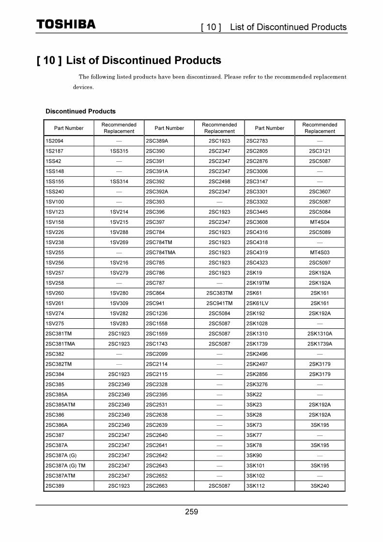
[ 10 ] List of Discontinued Products
259
[ 10 ] List of Discontinued Products
The following listed products have been discontinued. Please refer to the recommended replacement
devices.
Discontinued Products
Part Number Recommended
Replacement Part Number
Recommended
Replacement Part Number
Recommended
Replacement
1S2094 ⎯ 2SC389A 2SC1923 2SC2783 ⎯
1S2187 1SS315 2SC390 2SC2347 2SC2805 2SC3121
1SS42 ⎯ 2SC391 2SC2347 2SC2876 2SC5087
1SS148 ⎯ 2SC391A 2SC2347 2SC3006 ⎯
1SS155 1SS314 2SC392 2SC2498 2SC3147 ⎯
1SS240 ⎯ 2SC392A 2SC2347 2SC3301 2SC3607
1SV100 ⎯ 2SC393 ⎯ 2SC3302 2SC5087
1SV123 1SV214 2SC396 2SC1923 2SC3445 2SC5084
1SV158 1SV215 2SC397 2SC2347 2SC3608 MT4S04
1SV226 1SV288 2SC784 2SC1923 2SC4316 2SC5089
1SV238 1SV269 2SC784TM 2SC1923 2SC4318 ⎯
1SV255 ⎯ 2SC784TMA 2SC1923 2SC4319 MT4S03
1SV256 1SV216 2SC785 2SC1923 2SC4323 2SC5097
1SV257 1SV279 2SC786 2SC1923 2SK19 2SK192A
1SV258 ⎯ 2SC787 ⎯ 2SK19TM 2SK192A
1SV260 1SV280 2SC864 2SC383TM 2SK61 2SK161
1SV261 1SV309 2SC941 2SC941TM 2SK61LV 2SK161
1SV274 1SV282 2SC1236 2SC5084 2SK192 2SK192A
1SV275 1SV283 2SC1558 2SC5087 2SK1028 ⎯
2SC381TM 2SC1923 2SC1559 2SC5087 2SK1310 2SK1310A
2SC381TMA 2SC1923 2SC1743 2SC5087 2SK1739 2SK1739A
2SC382 ⎯ 2SC2099 ⎯ 2SK2496 ⎯
2SC382TM ⎯ 2SC2114 ⎯ 2SK2497 2SK3179
2SC384 2SC1923 2SC2115 ⎯ 2SK2856 2SK3179
2SC385 2SC2349 2SC2328 ⎯ 2SK3276 ⎯
2SC385A 2SC2349 2SC2395 ⎯ 3SK22 ⎯
2SC385ATM 2SC2349 2SC2531 ⎯ 3SK23 2SK192A
2SC386 2SC2349 2SC2638 ⎯ 3SK28 2SK192A
2SC386A 2SC2349 2SC2639 ⎯ 3SK73 3SK195
2SC387 2SC2347 2SC2640 ⎯ 3SK77 ⎯
2SC387A 2SC2347 2SC2641 ⎯ 3SK78 3SK195
2SC387A (G) 2SC2347 2SC2642 ⎯ 3SK90 ⎯
2SC387A (G) TM 2SC2347 2SC2643 ⎯ 3SK101 3SK195
2SC387ATM 2SC2347 2SC2652 ⎯ 3SK102 ⎯
2SC389 2SC1923 2SC2663 2SC5087 3SK112 3SK240
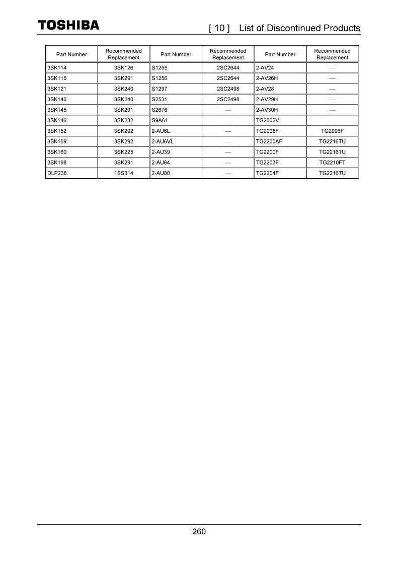
[ 10 ] List of Discontinued Products
260
Part Number Recommended
Replacement Part Number
Recommended
Replacement Part Number
Recommended
Replacement
3SK114 3SK126 S1255 2SC2644 2-AV24 ⎯
3SK115 3SK291 S1256 2SC2644 2-AV26H ⎯
3SK121 3SK240 S1297 2SC2498 2-AV28 ⎯
3SK140 3SK240 S2531 2SC2498 2-AV29H ⎯
3SK145 3SK291 S2676 ⎯ 2-AV30H ⎯
3SK146 3SK232 S9A61 ⎯ TG2002V ⎯
3SK152 3SK292 2-AU6L ⎯ TG2005F TG2006F
3SK159 3SK292 2-AU6VL ⎯ TG2200AF TG2216TU
3SK160 3SK225 2-AU39 ⎯ TG2200F TG2216TU
3SK198 3SK291 2-AU64 ⎯ TG2203F TG2210FT
DLP238 1SS314 2-AU80 ⎯ TG2204F TG2216TU