high-gain inverters based on wse complementary...
TRANSCRIPT

TOSUN ET AL . VOL. 8 ’ NO. 5 ’ 4948–4953 ’ 2014
www.acsnano.org
4948
March 31, 2014
C 2014 American Chemical Society
High-Gain Inverters Based on WSe2Complementary Field-Effect TransistorsMahmut Tosun,†,‡,§ Steven Chuang,†,‡,§ Hui Fang,†,‡,§ Angada B. Sachid,† Mark Hettick,†,‡,§ Yongjing Lin,†,‡,§
Yuping Zeng,†,‡,§ and Ali Javey†,‡,§,*
†Electrical Engineering and Computer Sciences, University of California, Berkeley, California 94720, United States, ‡Materials Sciences Division, Lawrence BerkeleyNational Laboratory, Berkeley, California 94720, United States, and §Berkeley Sensor and Actuator Center, University of California, Berkeley, California 94720, United States
Continued scaling of metal-oxide-semiconductor field-effect transis-tors (MOSFETs) has enabled lower
operating voltages, faster switching speeds,and enhanced computation power. How-ever, as the channel length of MOSFETsapproaches the sub-10 nm regime, severeshort channel effects deteriorate the switch-ing performance of the planar devices. Inthis regard, multiple device architectureshave been proposed for enhanced gatecoupling and reduced short channel effects.One approach involves the use of an ultra-thin-body semiconductor, where the entirethickness of the active channel is in closeproximity to the gate electrode, thereby en-hancing the gate control of the channel.1,2
As a rule of thumb, the thickness of thesemiconductor should be kept to ∼<1/3 of
the gate length for effective gate couplingof the device. For ultrashort channel de-vices, this corresponds to a semiconductorthickness on the order of only a few atomiclayers. This aggressive scaling possessessignificant challenges since at such thick-nesses any variation of the thickness, at theatomic scale, yields severe surface potentialvariation and thereby enhanced surfaceroughness scattering of the carriers. Layeredtransition metal dichalcogenides (TMDCs),such as MoS2 and WSe2, have been investi-gated as a promising material class for futurescaled devices, owing to their inherentthickness uniformity and control down toa monolayer.3�5 TMDC FETs have exhibitedexcellent metrics such as ON/OFF currentratios of up to 108,3 subthreshold swingsof 60 mV/dec,4 and electron and hole
* Address correspondence [email protected].
Received for review February 18, 2014and accepted March 31, 2014.
Published online10.1021/nn5009929
ABSTRACT
In this work, the operation of n- and p-type field-effect transistors (FETs) on the same WSe2 flake is realized,and a complementary logic inverter is
demonstrated. The p-FET is fabricated by contacting WSe2 with a high work function metal, Pt, which facilities hole injection at the source contact. The
n-FET is realized by utilizing selective surface charge transfer doping with potassium to form degenerately doped nþ contacts for electron injection. An
ON/OFF current ratio of >104 is achieved for both n- and p-FETs with similar ON current densities. A dc voltage gain of >12 is measured for the
complementary WSe2 inverter. This work presents an important advance toward realization of complementary logic devices based on layered chalcogenide
semiconductors for electronic applications.
KEYWORDS: transition metal dichalcogenides . digital circuits . monolayer semiconductors . complementary logic .CMOS electronics
ARTIC
LE

TOSUN ET AL . VOL. 8 ’ NO. 5 ’ 4948–4953 ’ 2014
www.acsnano.org
4949
mobilities of >100 cm2/(V s).4,6 To date, both n- andp-type transistors have been demonstrated on differ-ent flakes ofMoS2 andWSe2 through contact engineer-ing by using either low/highwork functionmetals and/or surface charge transfer doping.4,6�9 TMDC logicgates have also been demonstrated based on n-typeMoS2 FETs10�12 and resistor-loaded WSe2 devices.13
Moving forward, the demonstration of n- and p-typetransistors on the same substrate is needed to enablelow-power complementary MOS (CMOS) logic circuitsgiven their performance advantage over unipolar logiccircuits. Building on the recent advancements de-scribed above, here, we report the first operation ofn- and p-FETs on the same WSe2 flake, thereby en-abling the realization of TMDC CMOS logic gates.The polarity of a MOS transistor is determined by the
type of carriers (i.e., electrons versus holes) that thesource contact can supply to the semiconductor chan-nel. In conventional MOSFETs, this is achieved throughformation of degenerately doped nþ and pþ S/Dcontacts for n- and p-type operation, respectively. Onthe other hand, in Schottky barrier (SB) MOSFETs,where metal contacts are fabricated directly on topof the channel, the polarity is governed by the Schottkybarrier height (andwidth) for electrons and holes at thesource electrode. A low SB height to the conductionband yields electron injection into the channel, therebyresulting in n-type device operation. Similarly, a low SBheight to the valence band yields p-type characteristics.Heavy doping of the semiconductor region in the proxi-mity of the contacts can reduce the SB widths, therebyenabling efficient electron or hole injection through theSBs by a tunneling process. This results in a deviceconfiguration that resembles the conventional MOSFETs.Note that in all cases the effect of channel doping is tosimply control the threshold voltage of the device alongwith the contact electrostatics for short channel effects.The most commonly utilized device configuration
for TMDCs is the SB-MOSFET structure, with the twomost explored materials being MoS2 and WSe2. Giventhe low conduction band edge position (i.e., largeelectron affinity) of MoS2 and the Fermi level pinningnear the conduction band edge at themetal interfaces,most MoS2 SB-MOSFETs fabricated to date have beenn-type. On the other hand, the high valence band edgeposition of WSe2 readily results in p-type operation.Thus, to achieve robust CMOS operation based on asingle channel material system, the contacts need tobe degenerately doped, at least for one polarity de-pending on whether MoS2 or WSe2 is utilized. In thiswork, we focus onWSe2 as the semiconductormaterial.We achieve p-FETs by using high work function Ptcontacts configured in a SB-MOSFET geometry. On theother hand, n-FETs are obtained by degenerate dopingof the underlapped contact regions. This configurationprovides us with a platform to fabricate WSe2 CMOSdevices and logic gates.
Chemical doping of TMDCs, up to the degeneratelevel, has been previously reported by our group usingsurface charge transfer processes. Given the molecularthickness of TMDCs, by simply placing electron-donat-ing or -withdrawing species on their surfaces, n- andp-type doping can be obtained, respectively, at degen-erate carrier concentrations.4,8 This principal is similarto the doping process that has been extensively ex-plored in the past for organic semiconductors,14 carbonnanotubes,15�17 graphene,18 and nanoscale III�Vs.19
Surface charge transfer doping is distinct from substitu-tional doping since there is no replacement of latticeatoms, which is of advantage for nanoscale materials,where substitutional doping can lead to large stochasticvariation given the small number of atoms involved. Ourprevious work has shown that NO2 and potassium serveas efficient electron-withdrawing and -donating speciesfor WSe2, respectively.
4,8 By patterning the surface ofTMDCs prior to exposure to the dopants, doping profil-ing along the length of TMDCs can be readily obtained,thereby enabling fabrication of p- or n-FETs with degen-erately doped contacts. Here, we utilize patterned Kdoping for selective nþ doping of the contacts of then-FETs.Contacting the conduction band of WSe2 with ele-
mental metals is challenging;7 hence we used surfacecharge transfer doping to form degenerately dopednþ contact regions. To achieve patterned doping ofthe nþ contacts, a gate structure underlapping the S/Delectrodes is fabricated for the n-side, which acts as amask for the subsequent doping process. On the otherhand, an overlapped gate structure is formed on thep-side. The overlapped top gate structure of the p-FETprotects the integrity of the p-side channel duringpotassium doping. On the other hand, the exposedWSe2 regions near the metal electrodes of the n-sideare exposed to K atoms, leading to the formation of nþcontacts on either side of the gate. The heavy n-dopingof the contacts yields low resistance contacts to theconduction band of WSe2 for electron injection.8 Thefalse color SEM image of the fabricated CMOS inverterand the device schematic are shown in Figure 1a and b,respectively. The measurements of the devices aresubsequently performed in situ, withoutbreakingvacuumsince K doping is not air stable. In the future, explora-tion of air-stable dopants or encapsulation techniquesare needed to enhance the stability of the devices to airexposure.
RESULTS AND DISCUSSION
Device schematics for the WSe2 p- and n-FETs usedin this work are shown in Figure 2a and b, respectively.Figure 2c shows the drain current, ID, versus gatevoltage, VGS, curve at a drain voltage of VDS = �1 Vfor a WSe2 p-FET fabricated on a ∼10 nm thick flakewith Pt contacts. The channel length is L= 2μmand thegate electrode overlaps the S/D contacts. The device
ARTIC
LE

TOSUN ET AL . VOL. 8 ’ NO. 5 ’ 4948–4953 ’ 2014
www.acsnano.org
4950
exhibits clear p-type behavior with an ON/OFF currentratio of >104. The transistor has a threshold voltage (VT)of �2 V, as extracted by the linear extrapolation of theID�VGS curve. The negative VT of this p-FET makes it anenhancement mode device (i.e., OFF at VGS = 0 V),which is desired for CMOS logic circuit fabrication. TheON-current density of this long channel device at|VGS � VT| = 1 V is 0.1 μA/μm, as normalized by thewidth of the WSe2 flake. This ON current, while suffi-cient for proof-of-concept CMOS operation demon-strated in this work, is limited by the SB to the valenceband of WSe2 at the source contact. As shown pre-viously by our group, the ON current can be furtherimproved by contact doping to reduce the thickness ofSBs.4 Furthermore, channel length and gate dielectricthickness down-scaling is needed to further enhancethe ON-state drive currents.The transfer characteristic of an n-type FET fabri-
cated on the same flake as the one used for the p-FETdevice above is also shown in Figure 2c. Here, the
ID�VGS curves at VDS = 1 V are shown as a function of Kdoping time, up to 5 min. The channel length is 1 μm,and as discussed earlier the gate electrode underlapsthe metal S/D contacts. Since the entire gate stack,including the dielectric layer, was patterned by a lift-offprocess, there is no dielectric layer on the surface of theunderlapped WSe2 regions, making them directly ex-posed to the K vapor during the doping process. Themeasurements are performed in situ under vacuumsince K doping is not air stable. From Figure 2c it is clearthat the n-channel conduction increases as the dopingtime is increased due to the thinning of the SBs to theconduction band of WSe2. Note that, without doping,the ungated WSe2 regions on each side of the gateexhibit high sheet resistivity due to the low carrierconcentrations. In addition, in the absence of K doping,the high Schottky barrier height and width at themetal/WSe2 junction further limits electron injection.As a result, without doping, the underlapped devicedelivers no current drive (limited by the instrument
Figure 1. (a) False-color SEM image of a fabricated CMOS inverter on a singleWSe2 flake. (b) Schematic of the CMOS inverter,depicting the n- and p-FET components.
Figure 2. (a and b) Device schematics (not drawn to scale) of theWSe2 p- and n-FETs, respectively. (c) Transfer characteristicsatVDS = |1 V| of aWSe2 p-FET andn-FET fabricatedon the sameflake as a function of potassiumdoping time (1, 2, 3, and5min).The transfer characteristics of the p-FET remain unchanged after dopingdue to the gate overlap structure. For clarity, only thedata before doping are shown for the p-FET. (d) Extracted contact resistance, Rc, as a function of K doping time for p- andn-FETs.
ARTIC
LE
TOSUN ET AL . VOL. 8 ’ NO. 5 ’ 4948–4953 ’ 2014
www.acsnano.org
4951
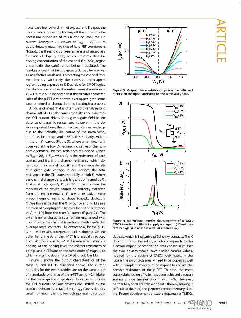
noise baseline). After 5 min of exposure to K vapor, thedoping was stopped by turning off the current to thepotassium dispenser. At this K doping level, the ONcurrent density is 0.2 μA/μm at |VGS � VT| = 2 V,approximately matching that of its p-FET counterpart.Notably, the threshold voltage remains unchanged as afunction of doping time, which indicates that thedoping concentration of the channel (i.e., WSe2 regionunderneath the gate) is not being modulated. Theresults suggest that the top gate stack used here servesas an effectivemask and is protecting the channel fromthe dopants, with only the exposed underlappedregions being exposed to K. Desirable for CMOS logics,the device operates in the enhancement mode withVT = 1 V. It should be noted that the transfer character-istics of the p-FET device with overlapped gate struc-ture remained unchanged during the doping process.A figure of merit that is often used to analyze long
channelMOSFETs is the carriermobility since it dictatesthe ON current drives for a given gate field in theabsence of parasitic resistances. However, in the de-vices reported here, the contact resistances are largedue to the Schottky-like nature of the metal/WSe2interfaces for both p- and n-FETs. This is clearly evidentin the ID�VD curves (Figure 3), where a nonlinearity isobserved at the low VD regime, indicative of the non-ohmic contacts. The total resistance of a device is givenas Rtot = 2Rc þ Rch, where Rc is the resistance of eachcontact and Rch is the channel resistance, which de-pends on the channel mobility and the charge densityat a given gate voltage. In our devices, the totalresistance in the ON-state, especially at high VG wherethe channel charge density is large, is dominated by Rc.That is, at high VG�VT, Rtot ≈ 2Rc. In such a case, themobility of the device cannot be correctly extractedfrom the experimental I�V curves. Instead, a moreproper figure of merit for these Schottky devices isRc. We have extracted the Rc of our p- and n-FETs as afunction of K doping time by calculating the resistanceat VG = |3 V| from the transfer curves (Figure 2d). Thep-FET transfer characteristics remain unchanged withdoping since the channel is protected with a gate thatoverlaps metal contacts. The extracted Rc for the p-FETis ∼1 Mohm-μm, independent of K doping. On theother hand, the Rc of the n-FET is drastically reducedfrom ∼0.5 Gohm-μm to ∼5 Mohm-μm after 5 min of Kdoping. At this doping level, the contact resistances ofboth p- and n-FETs are on the same order of magnitude,which makes the design of a CMOS circuit feasible.Figure 3 shows the output characteristics of the
same p- and n-FETs discussed above. The currentdensities for the two polarities are on the same orderof magnitude, with that of the n-FET being∼2� higherfor the same gate voltage drive. As discussed earlier,the ON currents for our devices are limited by thecontact resistances. In fact, the ID�VDS curves depict asmall nonlinearity in the low-voltage regime for both
devices, which is indicative of Schottky contacts. The Kdoping time for the n-FET, which corresponds to theelectron doping concentration, was chosen such thatthe two devices would have similar current values,needed for the design of CMOS logic gates. In thefuture, the p-contacts ideally need to be doped as wellwith a complementary surface dopant to reduce thecontact resistance of the p-FET. To date, the mostsuccessful p-doing ofWSe2 has been achieved throughsurface charge transfer doping with NO2. However,neither NO2 nor K are stable dopants, therebymaking itdifficult at this stage to perform complementary dop-ing. Future development of stable dopants for TMDCs
Figure 3. Output characteristics of p- (on the left) andn-FETs (on the right) fabricated on the same WSe2 flake.
Figure 4. (a) Voltage transfer characteristics of a WSe2CMOS inverter at different supply voltages. (b) Direct cur-rent voltage gain of the inverter at different VDD.
ARTIC
LE

TOSUN ET AL . VOL. 8 ’ NO. 5 ’ 4948–4953 ’ 2014
www.acsnano.org
4952
is required, which can further enhance the perfor-mance of CMOS devices.Next, we focus on configuring the complementary
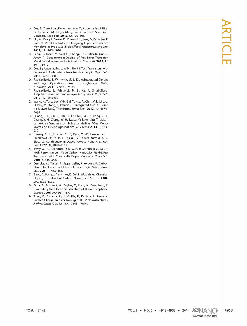
n- and p-FETs into CMOS logic circuits. As a proof ofconcept, an inverter gate (i.e., NOT logic gate) isdemonstrated using one n- and one p-FET connectedin series. In a conventional manner, the n-FET isgrounded and the supply voltage VDD is applied tothe p-FET. Both p- and n-FETs are controlled by thesame top gate electrode that serves as the inputvoltage (VIN) electrode. Output voltage (VOUT) is mea-sured using the common source electrode of the p-FETand n-FET. If a small input voltage is applied, the n-FETis OFF and p-FET is ON; therefore VOUT is connected toVDD. In other words, VOUT is pulled up to logic 1. On thecontrary, at high input voltages, the n-FET is ON andthe p-FET is OFF; therefore VOUT is connected to ground(0 V). In other words, VOUT is pulled down to logic 0. Thecircuit schematic of a CMOS inverter is shown in theinset of Figure 4a, with the false color SEM image of thefabricated device shown in Figure 1a. The transfercharacteristics (VOUT versus VIN) of the CMOS inverteras a function of VDD are shown in Figure 4a. Clear signalinversion is observed with high VOUT and low VIN andvice versa. The peak dc voltage gain of the CMOSinverter, |∂VOUT/∂VIN|, is measured to be >12 at a supplyvoltage VDD of 3 V (Figure 4b). The gain of the inverter is
high despite the nonoptimal transistor currents. Noisemargins are evaluated by extracting the maximum lowinput voltage VIL, minimum high input voltage VIH, mini-mumhighoutput voltageVOH, andmaximum lowoutputvoltageVOL.VIL andVIH are the input voltages atwhich theslope of the voltage transfer curve in Figure 4a is �1(unity gain), whereas VOH and VOL are the correspondingoutput voltages, respectively. The high- and low-statenoise margins (NMH and NML, respectively) are thencalculated by using the expressions NMH = VOH � VIHand NML = VIL � VOL. The noise margins are found to beNMH = 0.35VDD and NML = 0.32VDD for VDD = 3 V.
CONCLUSION
In conclusion, a CMOS inverter on the same TMDCflake, WSe2, is realized for the first time. The operationof the p-FET is realized by high-workfunction Pt con-tacts and overlapped top-gate device structure,whereas the n-FET is enabled by potassium doping ofthe contact regions using an underlapped top-gatestructure as a self-alignedmask. The results depict thatthrough proper contact engineering, both transistorpolarities can be obtained using the same TMDC on asingle substrate. Moving forward, further optimizationof the contacts and especially developing air-stableelectron and hole dopants are needed to explore theperformance limits of TMDC CMOS circuits.
METHODS AND EXPERIMENTAL SECTIONThe fabrication process of WSe2 CMOS devices is as follows.
WSe2 flakes were deposited on Si/SiO2 (thickness, 260 nm)substrates using a micromechanical exfoliation technique. Thetransferred flakes were mapped in terms of location, dimen-sions, and thickness using an optical microscope. Three elec-tron-beam (e-beam) lithography steps were performed in orderto define the p- and n-contacts as well as the top-gate stack.Specifically, a Pt/Au/Pd (10/30/20 nm) metal stack was depos-ited by e-beam evaporation for the p-side source�drain (S/D)contacts followed by lift-off in acetone. Subsequently, thedevices were annealed in O2 ambient at 250 �C for 1 h to furtherimprove the contact resistance. This metal stack was chosen forthe p-FETs due to the high work function of the Pt bottom layer,which provides a low Schottky barrier height for hole injectioninto the valence band of WSe2. As a result, WSe2 p-FETs arerealized as shown here. Au (60 nm) contacts were then formedfor the n-side S/D electrodes by e-beam evaporation and lift-offin acetone. The gate stacks are formed by e-beam lithography,atomic layer deposition (ALD) of ZrO2 (thickness, ∼20 nm) at120 �C, evaporation of Ni/Au electrodes (30/30 nm), and lift-offof the entire gate stack in acetone. Note that the low-tempera-ture ALD used here allows for the use of the lift-off process forthe entire gate stack using poly(methyl methacrylate) (PMMA)as the resist. Subsequently, potassium doping is performed ina vacuum at a pressure of 4 � 10�5 mbar by evaporatingpotassium from a commercially available dispenser filament(SAES Getters) by applying a 5 A dc current through it. Thedoping setup, which resembles a conventional thermal eva-porator in terms of operation principles, is designed such that ata sample distance of ∼3 cm from the potassium dispenser thedeposition of potassium is uniform over a 2 cm � 2 cm area,which is a typical chip size. The doping concentration is con-trolled through K evaporation time. Notably, the devices areelectrically measured in situ during the K evaporation process,
and once a desired doping level is reached, as confirmed fromthe electricalmeasurements, the current flow to the dispenser isstopped.
Conflict of Interest: The authors declare no competingfinancial interest.
Acknowledgment. This work was funded by the Director,Office of Science, Office of Basic Energy Sciences, MaterialSciences and Engineering Division of the U.S. Department ofEnergy, under Contract No. DE-AC02-05CH11231. A.B.S. wasfunded by ATMI, Inc. and Applied Materials, Inc. under the iRICEprogram.
REFERENCES AND NOTES1. Yang-Kyu, C.; Asano, K.; Lindert, N.; Subramanian, V.; Tsu-
Jae, K.; Bokor, J.; Chenming, H. Ultra-Thin Body SOIMOSFETfor Deep-Sub-Tenth Micron Era. Tech. Dig.�Int. ElectronDevices Meet. 1999, 919�921.
2. Kedzierski, J.; Xuan, P.; Subramanian, V.; Bokor, J.; King, T.-J.;Hu, C.; Anderson, E. A 20 nm Gate-Length Ultra-Thin Bodyp-MOSFET with Silicide Source/Drain. Superlattices Micro-struct. 2000, 28, 445–452.
3. Radisavljevic, B.; Radenovic, A.; Brivio, J.; Giacometti, V.; Kis,A. Single-Layer MoS2 Transistors. Nat. Nanotechnol. 2011,6, 147–150.
4. Fang, H.; Chuang, S.; Chang, T. C.; Takei, K.; Takahashi, T.;Javey, A. High-Performance Single Layered WSe2 p-FETswith Chemically Doped Contacts. Nano Lett. 2012, 12,3788–3792.
5. Wang, Q. H.; Kalantar-Zadeh, K.; Kis, A.; Coleman, J. N.;Strano, M. S. Electronics and Optoelectronics of Two-Dimensional TransitionMetal Dichalcogenides.Nat. Nano-technol. 2012, 7, 699–712.
ARTIC
LE
TOSUN ET AL . VOL. 8 ’ NO. 5 ’ 4948–4953 ’ 2014
www.acsnano.org
4953
6. Das, S.; Chen, H.-Y.; Penumatcha, A. V.; Appenzeller, J. HighPerformance Multilayer MoS2 Transistors with ScandiumContacts. Nano Lett. 2012, 13, 100–105.
7. Liu, W.; Kang, J.; Sarkar, D.; Khatami, Y.; Jena, D.; Banerjee, K.Role of Metal Contacts in Designing High-PerformanceMonolayer n-TypeWSe2 Field Effect Transistors. Nano Lett.2013, 13, 1983–1990.
8. Fang, H.; Tosun, M.; Seol, G.; Chang, T. C.; Takei, K.; Guo, J.;Javey, A. Degenerate n-Doping of Few-Layer TransitionMetal Dichalcogenides by Potassium. Nano Lett. 2013, 13,1991–1995.
9. Das, S.; Appenzeller, J. WSe2 Field Effect Transistors withEnhanced Ambipolar Characteristics. Appl. Phys. Lett.2013, 103, 103501.
10. Radisavljevic, B.; Whitwick, M. B.; Kis, A. Integrated Circuitsand Logic Operations Based on Single-Layer MoS2.ACS Nano 2011, 5, 9934�9938.
11. Radisavljevic, B.; Whitwick, M. B.; Kis, A. Small-SignalAmplifier Based on Single-Layer MoS2. Appl. Phys. Lett.2012, 101, 043103.
12. Wang, H.; Yu, L.; Lee, Y.-H.; Shi, Y.; Hsu, A.; Chin, M. L.; Li, L.-J.;Dubey, M.; Kong, J.; Palacios, T. Integrated Circuits Basedon Bilayer MoS2 Transistors. Nano Lett. 2012, 12, 4674–4680.
13. Huang, J.-K.; Pu, J.; Hsu, C.-L.; Chiu, M.-H.; Juang, Z.-Y.;Chang, Y.-H.; Chang, W.-H.; Iwasa, Y.; Takenobu, T.; Li, L.-J.Large-Area Synthesis of Highly Crystalline WSe2 Mono-layers and Device Applications. ACS Nano 2013, 8, 923–930.
14. Chiang, C. K.; Fincher, C. R.; Park, Y. W.; Heeger, A. J.;Shirakawa, H.; Louis, E. J.; Gau, S. C.; MacDiarmid, A. G.Electrical Conductivity in Doped Polyacetylene. Phys. Rev.Lett. 1977, 39, 1098–1101.
15. Javey, A.; Tu, R.; Farmer, D. B.; Guo, J.; Gordon, R. G.; Dai, H.High Performance n-Type Carbon Nanotube Field-EffectTransistors with Chemically Doped Contacts. Nano Lett.2005, 5, 345–348.
16. Derycke, V.; Martel, R.; Appenzeller, J.; Avouris, P. CarbonNanotube Inter- and Intramolecular Logic Gates. NanoLett. 2001, 1, 453–456.
17. Zhou, C.; Kong, J.; Yenilmez, E.; Dai, H. Modulated ChemicalDoping of Individual Carbon Nanotubes. Science 2000,290, 1552–1555.
18. Ohta, T.; Bostwick, A.; Seyller, T.; Horn, K.; Rotenberg, E.Controlling the Electronic Structure of Bilayer Graphene.Science 2006, 313, 951–954.
19. Takei, K.; Kapadia, R.; Li, Y.; Plis, E.; Krishna, S.; Javey, A.Surface Charge Transfer Doping of III�V Nanostructures.J. Phys. Chem. C 2013, 117, 17845–17849.
ARTIC
LE