high performance analog integrated circuit design: … · high performance analog integrated...
TRANSCRIPT

High Performance AnalogIntegrated Circuit Design:The Effect of Device Self-
Heating on Design Optimization
Ronald L. Carter, ProfessorAnalog Integrated Circuit Design Lab
Electrical Engineering Department
The University of Texas at Arlington

RLCarter: Analog IC Design with Self Heating 2
Analog IC Designwith Self-Heating� Heat Source/Temperature Effects� Thermal Equations/Analogy� Thermal Resistance Models� Effect of Thermal Resistance on
Device Biasing� Effect of Thermal Resistance on the
Circuit Performance� Conclusions/Future Work
RLCarter: Analog IC Design with Self Heating 3
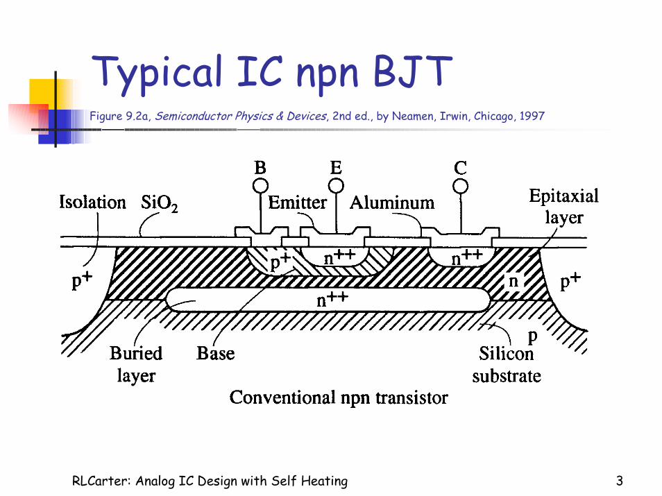
Typical IC npn BJTFigure 9.2a, Semiconductor Physics & Devices, 2nd ed., by Neamen, Irwin, Chicago, 1997

RLCarter: Analog IC Design with Self Heating 4
EB and CB Heat SourcesFigure 9.2a, Semiconductor Physics & Devices, 2nd ed., by Neamen, Irwin, Chicago, 1997
basecontact
emittercontact
colle
ctor
EB Depletion Region, PE = iE*v BEEB Depletion Region, PC = iC*v BC

RLCarter: Analog IC Design with Self Heating 5
Temperature Increase� Td-Ta=Ta{[1 + (n+1)(��e+��c)/Ta)]1/(n+1)1}��e and ��c are pseudo-temperatures via
the Kirchoff transformation,assuming k(T) = k(300K)�[T/300]n
� ��e = RTh,EB�|ievbe|� ��c = RTh,CB�|icvbc|� RTh,EB, RTh,CB are thermal res. at Ta.Following S. H. Whemple, and H. Huang, "Thermal Design of Power GaAs FETs", in GaAs FET Principles and
Technology, J. V. DiLorenzo and D. D. Khandelwal, eds., pp. 313-347, Artech House, 1982.

RLCarter: Analog IC Design with Self Heating 6
Circuit Simulation ofTemperature Effects� Typically TNOM (parameter spec.
temperature) and TEMP (circuitoperation temperature) only variables
� However, Td =Tdevice is a function of ie,vbe, ic and vbc.
� More flexibility with Vertical BipolarInter-Company model (VBIC)

RLCarter: Analog IC Design with Self Heating 7
Gummel-Poon Staticnpn Circuit Model
C
E
BB’
ILCILE IBF
IBR ICC - IEC =IS(exp(vBE/NFVt) -exp(vBC/NRVt)/QB
RC
RE
RBB
IntrinsicTransistor

RLCarter: Analog IC Design with Self Heating 8
VBIC Model Overview� Self-heating effects
included� Improved Early effect
modeling� Quasi-saturation modeling� Parasitic substrate
transistor modeling� Parasitic fixed (oxide)
capacitance modeling� An avalanche multiplication
model included� Base current is decoupled
from collector current

RLCarter: Analog IC Design with Self Heating 9
CAD Tools Support for VBIC� Hspice [4]
� Does not support PNP device� Does not scale with “Area” and “M” terms
� Spectre [5]
� Support both NPN and PNP devices� scale with “Area” and “M” term
� HPADS� No temperature nodes (“dt” and “tl”), so
unable to simulate thermal coupling effects

RLCarter: Analog IC Design with Self Heating 10
Temperature Designations forVBIC
25tnom27tnomParametersmeasurementtemperature 27tref
25
0Default
27
0Default NameName
temptempAmbient temperature
dtemptriseTemperature rise ofthe device fromambient
Hspice [5]Spectre [4]ParametersDescription

RLCarter: Analog IC Design with Self Heating 11
Using VBIC in Spectre [5]
Name c b e [s] [dt] [tl] ModelNameparameter=value ...
� Selft=1 and Rth>0 to enable Self-heating� 1 volt at the temperature nodes = 1 degree in
temperature� “tl” node represents the initial local temperature
of device which always corresponds totrise+temp
� “dt” node represents the rise above trise+tempcaused by thermal dissipation, whose value equalsV(dt)-V(tl)
� Device temperature=V(dt)-V(tl)+trise+temp
RLCarter: Analog IC Design with Self Heating 12
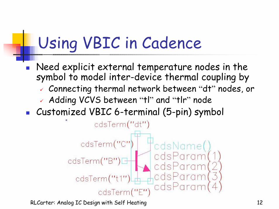
Using VBIC in Cadence� Need explicit external temperature nodes in the
symbol to model inter-device thermal coupling by� Connecting thermal network between “dt” nodes, or� Adding VCVS between “tl” and “tlr” node
� Customized VBIC 6-terminal (5-pin) symbol
RLCarter: Analog IC Design with Self Heating 13
Model Conversion� Most BJTs are defined with SGP model� A conversion from SGP to VBIC is needed� Only approximate conversion is possible� Some parameters are unmapped such as Rth and Cth
� Two approaches are provided� Manual conversion — done empirically and need Local
Ratio Evaluation [2]
� Program conversion using program sgp_2_vbic [3]

RLCarter: Analog IC Design with Self Heating 14
Parameter Mapping using sgp_2_vbicVBIC mapping VBIC mapping VBIC mappingRcx Rc Mc Mjc Xtf XtfRci 0 Cjcp Cjs Vtf VtfRbx Rbm Ps Vjs Itf ItfRbi Rb-Rbm Ms Mjs Tr TrRe Re Nei Nf Td �Tf·Ptf/180Is Is Iben Ise Ea EgNf Nf Nen Ne Eaie EgNr Nr Ibei Is/Bf Eaic EgFc Fc Ibci Is/Br Eane EgCje Cje Nci Nr Eanc EgPe Vje Ibcn Isc Xis XtiMe Mje Ncn Nc Xii Xti-XtbCjc Cjc·Xcjc Ikf Ikf Xin Xti-XtbCjep Cjc(1-Xcjc) Ikr Ikr Kfn KfPc Vjc Tf Tf Afn Af
AFFbcAR
Fbe
AF
C
F
VVVVV
IgO
//1/1��
�
AFRbcAR
Rbe
AR
e
R
VVVVV
Igo
//1/1��
�
��
���
�
�
��
����
�
�
����
�
�
����
�
�
����
�
�
�
�
11
1
1
/
/
ER
EF
eR
RbeR
beRbc
Fbe
cF
FbcF
bc
V
V
IgCqq
qIg
Cq
o
o
� Early Effect model isdifferent� Need Vbe, Vbc to solvethe 3 equations below

RLCarter: Analog IC Design with Self Heating 15
Analog IC Designwith Self-Heating� Heat Source/Temperature Effects� Thermal Equations/Analogy� Thermal Resistance Models� Effect of Thermal Resistance on
Device Biasing� Effect of Thermal Resistance on the
Circuit Performance� Conclusions/Future Work
RLCarter: Analog IC Design with Self Heating 16
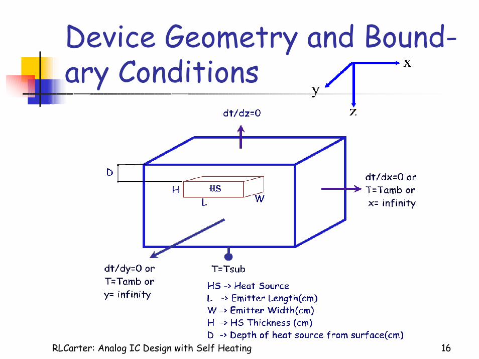
Device Geometry and Bound-ary Conditions

RLCarter: Analog IC Design with Self Heating 17
� �
�
�
�
���
������
V
zyxgzyxTT
2
Static Heat Flow Equationand Poisson s Equation
�T = T-T0 (K) is the temperature riseabove local ambient
� = Thermal conductivity (Wcm-1K-1)g= volumetric heat gen. rate (W cm-3)� = charge dens., and � = permittivity

RLCarter: Analog IC Design with Self Heating 18
The Electrical Analogy� The Kirchoff transformation factors
the �(T)� Both equations become the Laplacian� �V[Volt] is the analog of �T[K]� I[Ampere] is the analog of P [Watts]� V = IR is the analog of �T = P RTH

RLCarter: Analog IC Design with Self Heating 19
ParameterName
Si SiO2 Al Cu
Conductivity �(Wcm-1K-1)
1.412 0.014 2.37 3.98
Density�(g cm-3)
2.328 2.648 2.7 8.96
Specific HeatCP(Jg-1K-1)
0.7 0.787 0.898 0.384
Semiconductor MaterialProperties at 300K
RLCarter: Analog IC Design with Self Heating 20
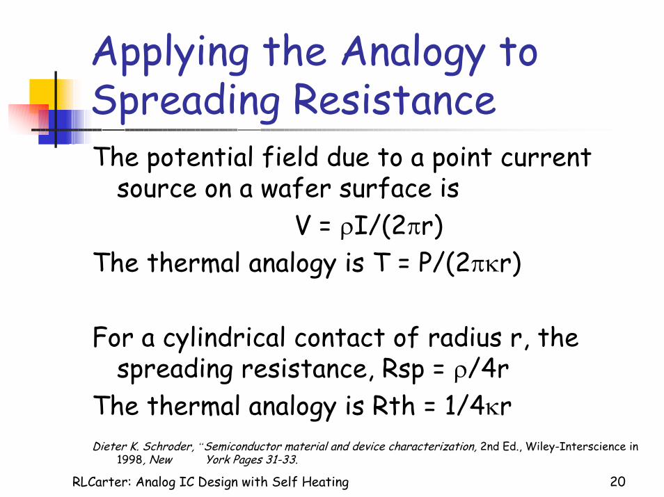
Applying the Analogy toSpreading ResistanceThe potential field due to a point current
source on a wafer surface isV = �I/(2�r)
The thermal analogy is T = P/(2��r)
For a cylindrical contact of radius r, thespreading resistance, Rsp = �/4r
The thermal analogy is Rth = 1/4�rDieter K. Schroder, “Semiconductor material and device characterization, 2nd Ed., Wiley-Interscience in
1998, New York Pages 31-33.

RLCarter: Analog IC Design with Self Heating 21
Analog IC Designwith Self-Heating� Heat Source/Temperature Effects� Thermal Equations/Analogy� Thermal Resistance Models� Effect of Thermal Resistance on
Device Biasing� Effect of Thermal Resistance on the
Circuit Performance� Conclusions/Future Work

RLCarter: Analog IC Design with Self Heating 22
Thermal Resistance Modelfor square emitter� For a square emitter of side w
S. H. Whemple, and H. Huang, op. cit.
t
w1k w )(TRR1-
wTnomSi,nomRTh,EBTh, �
�
���
����
�
�
� ��
t
w1k w )(TRR1-
wTnomSi,nomFTh,Th,CB �
�
���
����
�
�
� ��

RLCarter: Analog IC Design with Self Heating 23
Image effect of HeatSources Below Surface
basecontact
emittercontact
colle
ctor
EB Depletion Region, PE = iE*v BEEB Depletion Region, PC = iC*v BC
D
� �
lwt
DlwR
w
TH
��
�
�
thick, is wafer the
and surface the below D wide, w and long l is
emitter the where ,2/4
12
��

RLCarter: Analog IC Design with Self Heating 24
Dielectric Isolated BJT(DIBJT)
� kSi ~ 100 kSi02� Perimeter of “well”
is approximately anisotherm
� Rtrench = Rwall +Rsurface
� Rbulk = Risolation +Rsubstrate

RLCarter: Analog IC Design with Self Heating 25
DIBJT Rth Model

RLCarter: Analog IC Design with Self Heating 26
Analogy Modeling of DeviceThermal Resistance

RLCarter: Analog IC Design with Self Heating 27
Analog IC Designwith Self-Heating� Heat Source/Temperature Effects� Thermal Equations/Analogy� Thermal Resistance Models� Effect of Thermal Resistance on
Device Biasing� Effect of Thermal Resistance on the
Circuit Performance� Conclusions/Future Work

RLCarter: Analog IC Design with Self Heating 28
Transient Analysis of a BJTwith Multiple Thermal Paths
Simulation circuit� The thermal network consists of 3 poles� �1=1us, �2=100us and �3=10ms� Spectre� is used as a simulator

RLCarter: Analog IC Design with Self Heating 29
VBIC Model Parametersused for the BJTrcx 1� rci 0 rbx 36� rbi 0re 0.5� is 4.479fA nf 1.07 nr 1.07fc 0.5 cje 910fF pe 0.661 me 0.294cjc 417.5fF cjep 417.5fF pc 1 mc 0.28cjcp 0 ps 0.7 ms 0.5 nei 1.07iben 3.471pA nen 3.66 ibei 0.0172269fA ibci 4.479fAnci 1.07 ibcn 0 ncn 1 vef 195.325Vver 333.331V ikf 1mA ikr 0 tf 112psxtf 120V vtf 0 itf 0 tr 1nstd 0 ea 1.11 eaie 1.11 eaic 1.11eane 1.11 eanc 1.11 xis 3 xii 0.7
xin 0.7 kfn 0 afn 1
* Mapped from GP model

RLCarter: Analog IC Design with Self Heating 30
Transient ThermalResponse - JI BJT
10-10
10-8
10-6
10-4
10-2
0
1
Col
lect
or C
urre
nt (m
A)
Time (s )
Current and Temperature Ris e of a BJT with 3-P ole Thermal Network
CurrentTemperature Ris e
10-10
10-8
10-6
10-4
10-2
0
10
20
Tem
pera
ture
Ris
e (D
egre
e)
�1 �2 �3

RLCarter: Analog IC Design with Self Heating 31
Transient ThermalResponse - DIBJT
� RTH,epi=394 K/W� CTH,epi=79.4p sW/K
( �epi=31.3ns )
� RTH,ox=2742 K/W� CTH,ox=39.75p
sW/K
( �ox=109ns )
� RTH,w=126 K/W� CTH,w=11.9p sW/K
( �w=1.5ms )10-10 10-8 10-6 10-4 10-20
0.5
1
1.5
Col
lect
or C
urre
nt (m
A)
Time (s )
A DIBJT with 3-P ole Thermal Network
CurrentTemperature Ris e
10-10 10-8 10-6 10-4 10-20
10
20
30
Tem
pera
ture
Ris
e (D
egre
e)
�epi �ox �w

RLCarter: Analog IC Design with Self Heating 32
Build SDD BJT model inADS� SDD (Symbolic Defined Device)� Combination of the classical GP model and the
thermal network� For static model, IS, BF, BR, ISE and ISC
values changed by temperature rise

RLCarter: Analog IC Design with Self Heating 33
SDD Model verification
0 1 2 3 4 5 6-1
0
1
2
3
4
5
6
Col
lect
or c
urre
nt (m
A)
Vce (v)
I-V Characteris tics Comparis on of Different Models
S pectre VBIC modelADS GP modelADS S DD model
IB=25uA
IB=50uA
IB=75uA
IB=100uA
RLCarter: Analog IC Design with Self Heating 34
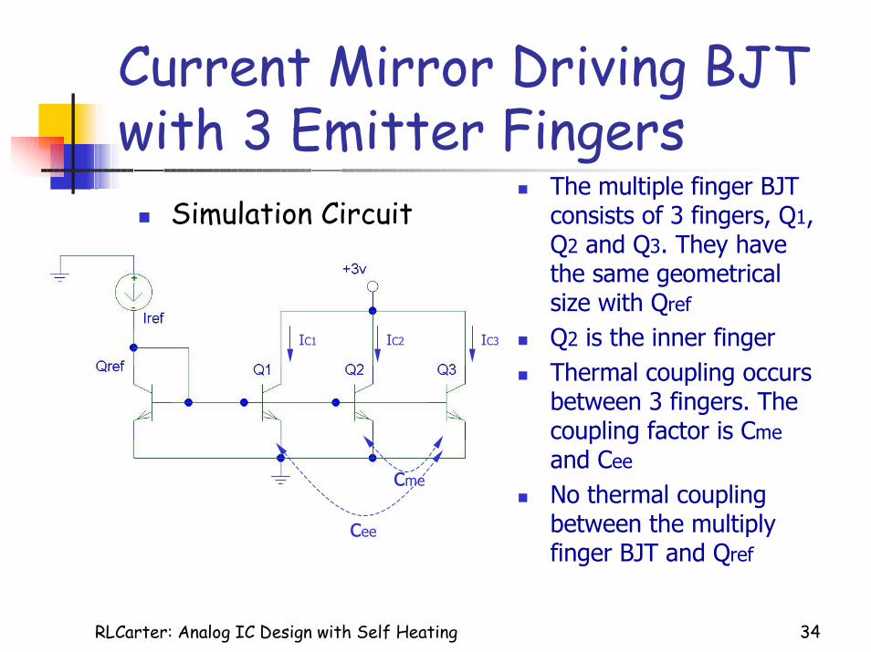
Current Mirror Driving BJTwith 3 Emitter Fingers
� Simulation Circuit� The multiple finger BJT
consists of 3 fingers, Q1,Q2 and Q3. They havethe same geometricalsize with Qref
� Q2 is the inner finger� Thermal coupling occurs
between 3 fingers. Thecoupling factor is Cmeand Cee
� No thermal couplingbetween the multiplyfinger BJT and Qref
IC1 IC2 IC3
cme
cee

RLCarter: Analog IC Design with Self Heating 35
VCVS Thermal CouplingModel

RLCarter: Analog IC Design with Self Heating 36
Model ParametersIS 1�10-18A BF 100 RE 5�
ISE 1�10-18A NF 1.07 RC 5�ISC 0 NR 1.07 RB 10�IKF 10mA NC 2 RBM 10�IKR � NE 1.259 EG 1.11eVIRB � VAF 74.03V XTI 3BR 0.7371 VAR 500V XTB 1.5
* Typical values for 1um�2um device

RLCarter: Analog IC Design with Self Heating 37
Current Ratio (IC/Iref) forDifferent RTH
0.051cee
0.102cme
3umS2umL1umW
0 0.5 1 1.5 2 2.5 3 3.5 40.8
1
1.2
1.4
1.6
1.8
2
2.2
2.4
2.6
2.8
Iref (mA)
Cur
rent
Rat
io
�Rth=3000K/W
�
Rth=1000K/W
�
Rth=300K/W
Inner emitterOuter emitter
1um�2um device

RLCarter: Analog IC Design with Self Heating 38
Temperature Rise forDifferent RTH
0 0.5 1 1.5 2 2.5 3 3.5 40
20
40
60
80
100
120
Iref (mA)
Tem
pera
ture
Ris
e (D
egre
e)
�Rth=3000K/W
�Rth=1000K/W
�Rth=300K/W
Inner fingerOuter finger
0.051cee
0.102cme
3umS2umL1umW
1um�2um device

RLCarter: Analog IC Design with Self Heating 39
Current Ratio forDifferent Spacing
0.0280.0577um
0.0360.0735um
0.0510.1023umCeeCme
RTH=3000 K/W
0 0.5 1 1.5 2 2.5 3 3.5 40.8
1
1.2
1.4
1.6
1.8
2
2.2
2.4
2.6
2.8
Iref (mA)
Cur
rent
Rat
io
�No thermal coupling
Inner emitterOuter emitter
5um
7um
3um
L=2um W=1um

RLCarter: Analog IC Design with Self Heating 40
Temperature Rise forDifferent Spacing
0.0280.0577um
0.0360.0735um
0.0510.1023umCeeCme
RTH=3000 K/W
0 0.5 1 1.5 2 2.5 3 3.5 40
20
40
60
80
100
120
Iref (mA)
Tem
pera
ture
Ris
e (D
egre
e)
�No thermal coupling
Inner emitterOuter emitter
5um
7um
3um
L=2um W=1um

RLCarter: Analog IC Design with Self Heating 41
0 0.5 1 1.5 2 2.5 3 3.5 4 4.5 50.8
1
1.2
1.4
1.6
1.8
2
2.2
2.4
2.6
Iref (mA)
Cur
rent
Rat
io
�Rth=2000K/W�
Rth=1000K/W
�
Rth=200K/W
Inner emitterOuter emitter
Current Ratio (IC/Iref) forDifferent RTH
0.050cee
0.100cme
3umS5umL1umW
1um�5um device

RLCarter: Analog IC Design with Self Heating 42
0 0.5 1 1.5 2 2.5 3 3.5 4 4.5 50
10
20
30
40
50
60
70
80
90
100
Iref (mA)
Tem
pera
ture
Ris
e (D
egre
e)
�Rth=2000K/W �Rth=1000K/W
�Rth=200K/W
Inner emitterOuter emitter
Temperature Rise forDifferent RTH
0.050cee
0.100cme
3umS5umL1umW
1um�5um device

RLCarter: Analog IC Design with Self Heating 43
Current Ratio forDifferent Spacing
0 0.5 1 1.5 2 2.5 3 3.5 4 4.5 50.8
1
1.2
1.4
1.6
1.8
2
2.2
2.4
2.6
Iref (mA)
Cur
rent
Rat
io
�No the rma l coupling
Inner emitterOuter emitter
0.0330.0677um
0.0400.0805um
0.0500.1003umCeeCme
RTH=2000 K/W
5um
7um
3um
L=5um W=1um

RLCarter: Analog IC Design with Self Heating 44
0 0.5 1 1.5 2 2.5 3 3.5 4 4.5 50
10
20
30
40
50
60
70
80
90
100
Iref (mA)
Tem
pera
ture
Ris
e (D
egre
e)
�No the rma l coupling
Inner emitterOuter emitter
Temperature Rise forDifferent Spacing
RTH=2000 K/W
L=5um W=1um 5um
7um
3um
0.0330.0677um
0.0400.0805um
0.0500.1003umCeeCme

RLCarter: Analog IC Design with Self Heating 45
Analog IC Designwith Self-Heating� Heat Source/Temperature Effects� Thermal Equations/Analogy� Thermal Resistance Models� Effect of Thermal Resistance on
Device Biasing� Effect of Thermal Resistance on the
Circuit Performance� Conclusions/Future Work

RLCarter: Analog IC Design with Self Heating 46
�A741 Simulation� Simulated by Spectre (Ver. 4.4.6.061301)� Analog Waveform is used to obtain graphic output� Use the circuit posted on WEB (http://www-
ee.uta.edu/Online/adavis/analog/f_opamp.cir)� Transistor models are mapped to VBIC model using
sgp_2_vbic (only one npn and pnp model used)� Area of Q13A is 0.25; Area of Q13B is 0.75� Areas of Q14 and Q20 are 3� Areas of other transistors are 1� Connect �A741 with �15V voltage supplies

RLCarter: Analog IC Design with Self Heating 47
µA741 Op-Amp Schematic [1]

RLCarter: Analog IC Design with Self Heating 48
Relative DeviceTemperatures
� Configure �A741as a voltagefollower
� DC analysis result� Rth for all npn
transistors is5000K/W
� Rth for all pnptransistors is1000KW
� No load isconnected
Temper at ur e def l ect i on
0
20
40
60
80
100
1 3 5 7 9 11 13 15 17 19 21 23Tr ans i s t or
Degr
ee
Q17 is 91 degrees higher than the ambient temperature!

RLCarter: Analog IC Design with Self Heating 49
Temperature transitions ofQ1 and Q13 (without Cth)
Q17
Q13
(Rth,npn=5000 K/W;Rth,pnp=1000 K/W)

RLCarter: Analog IC Design with Self Heating 50
Temperature transition ofQ17 (1)
� Rth,npn=5000K/W� Cth,npn=1� sW/K� Rth,pnp=1000K/W� Cth,pnp=10� sW/KNeed about 60msto reach thestable temperature
RLCarter: Analog IC Design with Self Heating 51
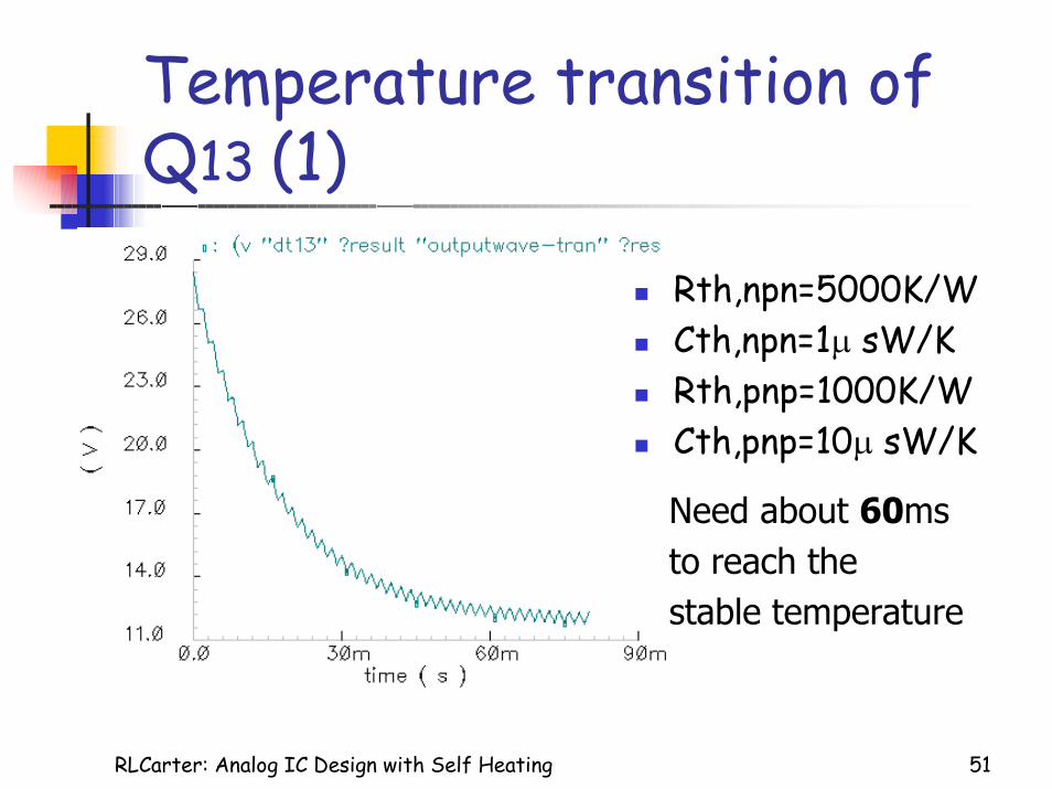
Temperature transition ofQ13 (1)
� Rth,npn=5000K/W� Cth,npn=1� sW/K� Rth,pnp=1000K/W� Cth,pnp=10� sW/K
Need about 60msto reach thestable temperature

RLCarter: Analog IC Design with Self Heating 52
Temperature transition ofQ17 (2)
� Need about40ms to reachthe stabletemperature
� Temperature var-iation increases
� Rth,npn=5000K/W� Cth,npn=0.1�sW/K� Rth,pnp=1000K/W� Cth,pnp=10� sW/K

RLCarter: Analog IC Design with Self Heating 53
Temperature transition ofQ13 (2)
� Need about10ms to reachthe stabletemperature
� Temperature var-iations increase
� Rth,npn=5000K/W� Cth,npn=1� sW/K� Rth,pnp=1000K/W� Cth,pnp=1� sW/K

RLCarter: Analog IC Design with Self Heating 54
Circuit used to measure theopen loop gain[2]
� Use a feedback technique todetermine the open loop gain
� DUT is the op amp to betested
� Nulling op amp is connectedin a feedback mode
� R1=100� R2=1M� R3=1K� Vmid=0� VSRC1 sweeps
from 0 to 1V
Simulation parameters:

RLCarter: Analog IC Design with Self Heating 55
Typical simulation output
RLCarter: Analog IC Design with Self Heating 56
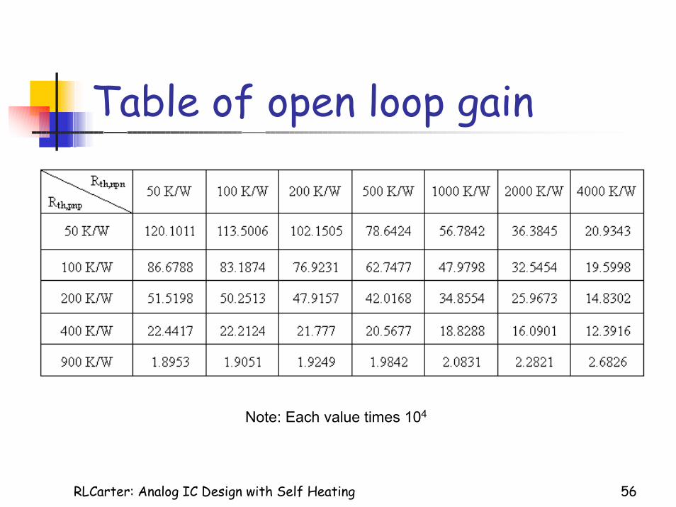
Table of open loop gain
Note: Each value times 104

RLCarter: Analog IC Design with Self Heating 57
Surface of open loop gain
� Interpolationused
� Decreasesabout afactor of 60!
22.5
33.5
1.82
2.22.4
2.62.8
2
4
6
8
10
12
x 105
log10(Rth,pnp)
log10(Rth,npn)
Ope
n Lo
op G
ain
RLCarter: Analog IC Design with Self Heating 58
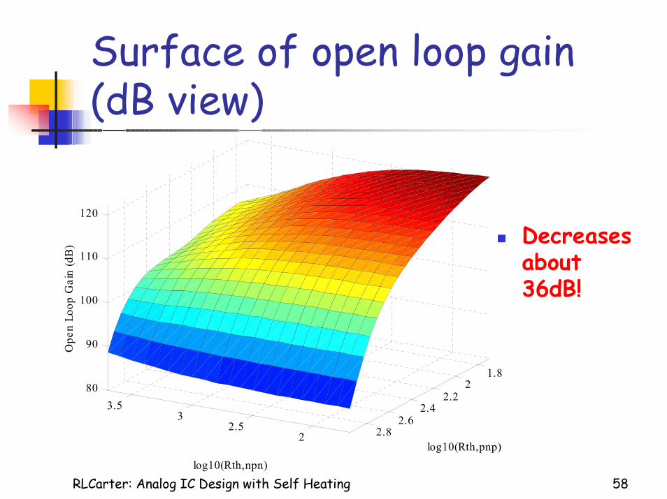
Surface of open loop gain(dB view)
� Decreasesabout36dB!
22.5
33.5
1.82
2.22.4
2.62.8
80
90
100
110
120
log10(Rth,pnp)log10(Rth,npn)
Ope
n Lo
op G
ain
(dB
)

RLCarter: Analog IC Design with Self Heating 59
Slew rate (without Cth )� Voltage follower is
used� Input signal
� 5K pulse input� rise and fall time: 1�S
� Voltage level: 0 and 10V� Rising edge is measured
� Unit: V/�S
Only 2% variation

RLCarter: Analog IC Design with Self Heating 60
Slew rate (including Cth )Set Rth,npn=5000 K/W and Rth,pnp=1000 K/W
� Only 0.4% variation when Cth changes� Comparing with Cth=0 case (0.6751, circled
value at previously table), only 1.5% variation� Self-heating (isolated) has no significant effect
on slew rate

RLCarter: Analog IC Design with Self Heating 61
Thermal coupling effect onopen-loop gain
� Use the same circuit discussed previously� Set Rth,npn=4000 K/W and Rth,pnp=900 K/W and
Cth,npn=Cth,pnp=0� The hottest transistor is Q17
� The amplificatory transistors at 1st stage are Q3 and Q4
� Temperature node of Q17 is connected with temperaturenode of Q3 and Q4 by two identical thermal resistors RC

RLCarter: Analog IC Design with Self Heating 62
Open-loop gain reduced bythermal coupling
101 102 103 104 105 1061.9
2
2.1
2.2
2.3
2.4
2.5
2.6
2.7x 10
4
Coupling Thermal Res is tor
Ope
n Lo
op G
ain
� Interpolationis used toobtain thiscurve
� Decreaseabout 25.4%!

RLCarter: Analog IC Design with Self Heating 63
Analog IC Designwith Self-Heating� Heat Source/Temperature Effects� Thermal Equations/Analogy� Thermal Resistance Models� Effect of Thermal Resistance on
Device Biasing� Effect of Thermal Resistance on the
Circuit Performance� Conclusions/Future Work
RLCarter: Analog IC Design with Self Heating 64
Summary� VBIC model used to analyze thermal effects
� Effect of individual device temperatures in a �A741� Inter-device heating effects
� Isolated self-heating in �A741� Isolated self-heating can reduce the open loop gain� Not a significant change in slew rate
� Preliminary study on thermal coupling effect� Open loop gain is reduced if significant thermal coupling
exists between 1st and 2nd stage� Current mirror temperature compensation schemes are
more critical when coupling is not optimum.

RLCarter: Analog IC Design with Self Heating 65
Acknowledgements: Support
� TheTexas Higher Education CoordinatingBoard (THECB)
� National Semiconductor Corporation (NSC)� The National Science Foundation
Industry/University Center for ElectronicMaterials, Devices and Systems(NSF/CEMDAS)

RLCarter: Analog IC Design with Self Heating 66
Acknowledgements:Analog IC Research Group� Professor W. Alan Davis� Zhipeng Zhu� Zheng Li� Siddharth Nashiney� Naveen Kumar Reddy Siddareddygari� Shankaranarayanan Rajaraman� Piyush Thacker� Anurag Lakhlani

RLCarter: Analog IC Design with Self Heating 67
ReferencesPaul R. Gray, Robert G. Meyer, et al, Analysis and design of analog integrated circuits, New York: Wiley, c2001
Fujiang Lin, et al, “Extraction Of VBIC Model for SiGe HBTs Made Easy by Going Through Gummel-Poon Model”,from http://eesof.tm.agilent.com/pdf/VBIC_Model_Extraction.pdf
http://www.fht-esslingen.de/institute/iafgp/neu/VBIC/
Avanti Star-spice User Manual, 04, 2001.
Affirma Spectre Circuit Simulator Device Model Equations
Zweidinger, D.T.; Fox, R.M., et al, “Equivalent circuit modeling of static substrate thermal coupling using VCVSrepresentation”, Solid-State Circuits, IEEE Journal of , Volume: 2 Issue: 9 , Sept. 2002, Page(s): 1198 -1206
Jonathan S. Brodsky, “Physics based impedance models for the simulation of self-heating in semiconductordevices and circuits”, PhD Dissertation, Dept of Electrical and Computer Engineering, University of Florida,Gainesville, Aug 1997.
McAndrew, C., Seitchik, J. and etal, ” VBIC95: An improved vertical, IC bipolar transistor model”,Bipolar/BiCMOS Circuits and Technology Meeting, 1995., Proceedings of the 1995
Burns and Robert, An introduction to mixed-signal testing, Oxford University Press, 1999 Copyright Texas Instruments