high-performance drams in workstation environments...
TRANSCRIPT

High-Performance DRAMsin Workstation Environments
Vinodh Cuppu, Student Member, IEEE, Bruce Jacob, Member, IEEE,
Brian Davis, Member, IEEE, and Trevor Mudge, Fellow, IEEE
AbstractÐThis paper presents a simulation-based performance study of several of the new high-performance DRAM architectures,
each evaluated in a small system organization. These small-system organizations correspond to workstation-class computers and use
only a handful of DRAM chips (~10, as opposed to ~1 or ~100). The study covers Fast Page Mode, Extended Data Out, Synchronous,
Enhanced Synchronous, Double Data Rate, Synchronous Link, Rambus, and Direct Rambus designs. Our simulations reveal several
things: 1) Current advanced DRAM technologies are attacking the memory bandwidth problem but not the latency problem; 2) bus
transmission speed will soon become a primary factor limiting memory-system performance; 3) the post-L2 address stream still
contains significant locality, though it varies from application to application; 4) systems without L2 caches are feasible for low- and
medium-speed CPUs (1GHz and below); and 5) as we move to wider buses, row access time becomes more prominent, making it
important to investigate techniques to exploit the available locality to decrease access time.
Index TermsÐDRAM architectures, DRAM performance, DRAM systems, system modeling, DDR DRAM, Direct Rambus DRAM,
PC100 SDRAM, DDR2 DRAM.
æ
1 INTRODUCTION
IN response to the growing gap between memory accesstime and processor speed, DRAM manufacturers have
created several new DRAM architectures. This paperpresents a simulation-based performance study of arepresentative group, evaluating each in terms of its effecton total execution time. We simulate the performance ofseven DRAM architectures: Fast Page Mode [36], ExtendedData Out [19], Synchronous [20], Enhanced Synchronous[13], Double Data Rate [21], Synchronous Link [38], Rambus[32], and Direct Rambus [33]. While there are a number ofacademic proposals for new DRAM designs, space limits usto covering only existing commercial architectures. Toobtain accurate memory-request timing for an aggressiveout-of-order processor, we integrate our code into theSimpleScalar tool set [4].
This paper presents a baseline study of a small-systemDRAM organization: These are systems with only a handfulof DRAM chips (0.1-1GB). We do not consider large-systemDRAM organizations with many gigabytes of storage thatare highly interleaved. We also study a set of benchmarksthat are appropriate for such systems: user-class applica-tions, such as compilers and small databases, rather thanserver-class applications, such as transaction processing
systems. The study asks and answers the followingquestions:
. What is the effect of improvements in DRAMtechnology on the memory latency and bandwidthproblems?
Contemporary techniques for improving proces-sor performance and tolerating memory latency areexacerbating the memory bandwidth problem [5].Our results show that current DRAM architecturesare attacking exactly this problem: The most recenttechnologies (SDRAM, ESDRAM, DDR, and Ram-bus) have reduced the stall time due to limitedbandwidth by a factor of three compared to earlierDRAM architectures. However, the memory-latencycomponent of overhead has not improved.
. Where is time spent in the primary memory system(the memory system beyond the cache hierarchy, butnot including secondary [disk] or tertiary [backup]storage)? What is the performance benefit ofexploiting the page mode of contemporary DRAMs?
For the newer DRAM designs, the time to extractthe required data from the sense amps/row cachesfor transmission on the memory bus is the largestcomponent in the average access time, though pagemode allows this to be overlapped with columnaccess and the time to transmit the data over thememory bus.
. How much locality is there in the address streamthat reaches the primary memory system?
The stream of addresses that miss the L2 cachecontains a significant amount of locality as measuredby the hit-rates in the DRAM row buffers. The hitrates for the applications studied range 2-97 percent,with a mean hit rate of 40 percent for a 1MB L2
IEEE TRANSACTIONS ON COMPUTERS, VOL. 50, NO. 11, NOVEMBER 2001 1133
. V. Cuppu and B. Jacob are with the Department of Electrical and ComputerEngineering, University of Maryland, College Park, College Park, MD20742. E-mail: {ramvinod, blj}@eng.umd.edu.
. B. Davis is with the Department of Electrical and Computer Engineering,Michigan Technological University, Houghton, MI 49931-1295.E-mail: [email protected].
. T. Mudge is with the Department of Electrical Engineering and ComputerScience, University of Michigan, Ann Arbor, MI 48109-2122.E-mail: [email protected].
Manuscript received 5 Dec. 2000; revised 25 May 2001; accepted 31 May2001.For information on obtaining reprints of this article, please send e-mail to:[email protected], and reference IEEECS Log Number 114256.
0018-9340/01/$10.00 ß 2001 IEEE

cache. (This does not include hits to the row bufferswhen making multiple DRAM requests to read onecache-line.)
. Does it make sense to eliminate the L2 cache in low-cost systems?
Modern DRAM designs are increasing theamount of SRAM and other cache-like storage onthe DRAM die [12]. In most cases, a memory systemcomprised of multiple DRAM chips will have manykilobytes of high-speed memory (for example, 8KBof high-speed storage per DRAM is common todayand the amount is increasing quickly). Our simula-tions show that, for low- and medium-speed CPUs(1GHz and under), it is possible to eliminate the L2cache and still have very reasonable performance.
We also make several observations. First, there is a one-time trade-off between cost, bandwidth, and latency: To apoint, latency can be decreased by ganging togethermultiple DRAMs into a wide structure. One can essentiallypay for bandwidth and simultaneously reduce latency: Arequest size is typically much larger than the DRAMtransfer width and the increased bandwidth improves thetransfer time of the large request. Both page mode andinterleaving exploit this phenomenon. However, once thebus is as wide as the request size, the benefit diminishes,and, to obtain further improvements, one must run theDRAM core and bus at faster speeds. Though currentmemory buses are adequate for current low- to mid-endsystems, they are inadequate for high-end systems. Widerbuses via embedded DRAM [5], [23], [37] are not a near-term solution, as embedded DRAM performance is poor onhigh-end workloads [3]. Faster buses are more likelysolutionsÐwitness the elimination of the slow intermediatememory bus in future systems [16]. Another solution is tointernally bank the memory array into many small arrays sothat each can be accessed very quickly, as in the MoSysMultibank DRAM architecture [39].
Second, widening buses will present new optimizationopportunities. Each application exhibits a different degreeof locality and therefore benefits from page mode to adifferent degree. As buses widen, this effect becomes morepronounced to the extent that different applications canhave average access times that differ by a factor of two. Thisis a minor issue considering current bus technology.However, future bus technologies will expose the rowaccess as a primary performance bottleneck, justifying theexploration of mechanisms that exploit locality to guaranteehits in the DRAM row buffers: e.g., row-buffer victimcaches, prediction mechanisms, etc. Note that recentcommercial DRAM proposals address exactly this issue byplacing associative SRAM caches on the DRAM die toexploit locality and the tremendous bandwidth availableon-chip [12].
Third, while buses as wide as the L2 cache yield the bestmemory latency, they have passed the point of diminishingreturns: For instance, a bus half as wide would not yieldtwice the latency. The use of page mode overlaps thecomponents of DRAM access when making multiplerequests to the same row, and one can only exploit thisoverlap when a cache block is larger than the bus widthÐ
otherwise, every cache-fill request requires one row accessand one column access. Therefore, the DRAM bus shouldnot exceed N/2 bits, where N is the L2 cache width.
Fourth, we note that, for the applications studied, totalexecution time seems to correlate more with end-to-endDRAM latencies than with critical-word latencies.
Finally, the choice of refresh mechanism can significantlyalter the average memory access time. For some bench-marks and some refresh organizations, the amount of timespent waiting for a DRAM in refresh mode accounted for50 percent of the total latency.
As one might expect, our results and conclusions aredependent on our system specifications, which we chose tobe representative of mid- to high-end workstations: a100MHz 128-bit memory bus (an organization that is foundin SPARC workstations and has the same bandwidth as aDRDRAM channel), an eight-way superscalar out-of-orderCPU, lockup-free caches, and a small-system DRAMorganization with ~10 DRAM chips.
2 RELATED WORK
Burger et al. quantified the effect on memory behavior ofhigh-performance latency-reducing or latency-toleratingtechniques, such as lockup-free caches, out-of-order execu-tion, prefetching, speculative loads, etc. [5]. They concludedthat, to hide memory latency, these techniques oftenincrease the demands on memory bandwidth. They classifymemory stall cycles into two types: those due to lack ofavailable memory bandwidth and those due purely tolatency. This is a useful classification, and we use it in ourstudy. This study differs from theirs in that we focus on theaccess time of only the primary memory system, while theirstudy combines all memory access time, including the L1and L2 caches. Their study focuses on the behavior oflatency-hiding techniques, while this study focuses on thebehavior of different DRAM architectures.
Several marketing studies compare the memory latencyand bandwidth available from different DRAM architec-tures [6], [30], [31]. This paper builds on these studies bylooking at a larger assortment of DRAM architectures,measuring DRAM impact on total application performance,decomposing the memory access time into differentcomponents, and measuring the hit rates in the row buffers.
Finally, there are many studies that measure system-wide performance, including that of the primary memorysystem [1], [2], [10], [22], [26], [27], [34], [35]. Our resultsresemble theirs in that we obtain similar figures for thefraction of time spent in the primary memory system.However, these studies have different goals from ours inthat they are concerned with measuring the effects on totalexecution time of varying several CPU-level parameters,such as issue width, cache size and organization, number ofprocessors, etc. This study focuses on the performancebehavior of different DRAM architectures.
3 BACKGROUND
A Random Access Memory (RAM) that uses a singletransistor-capacitor pair for each binary value (bit) isreferred to as a Dynamic Random Access Memory or
1134 IEEE TRANSACTIONS ON COMPUTERS, VOL. 50, NO. 11, NOVEMBER 2001
DRAM. This circuit is dynamic because leakage requires
that the capacitor be periodically refreshed for information
retention. Initially, DRAMs had minimal I/O pin counts
because the manufacturing cost was dominated by the
number of I/O pins in the package. Due largely to a desire
to use standardized parts, the initial constraints limiting the
I/O pins have had a long-term effect on DRAM architec-
ture: The address pins for most DRAMs are still multi-
plexed, potentially limiting performance. As the standard
DRAM interface has become a performance bottleneck, a
number of ªrevolutionaryº proposals [28] have been made.
In most cases, the revolutionary portion is the interface or
access mechanism, while the DRAM core remains essen-
tially unchanged.
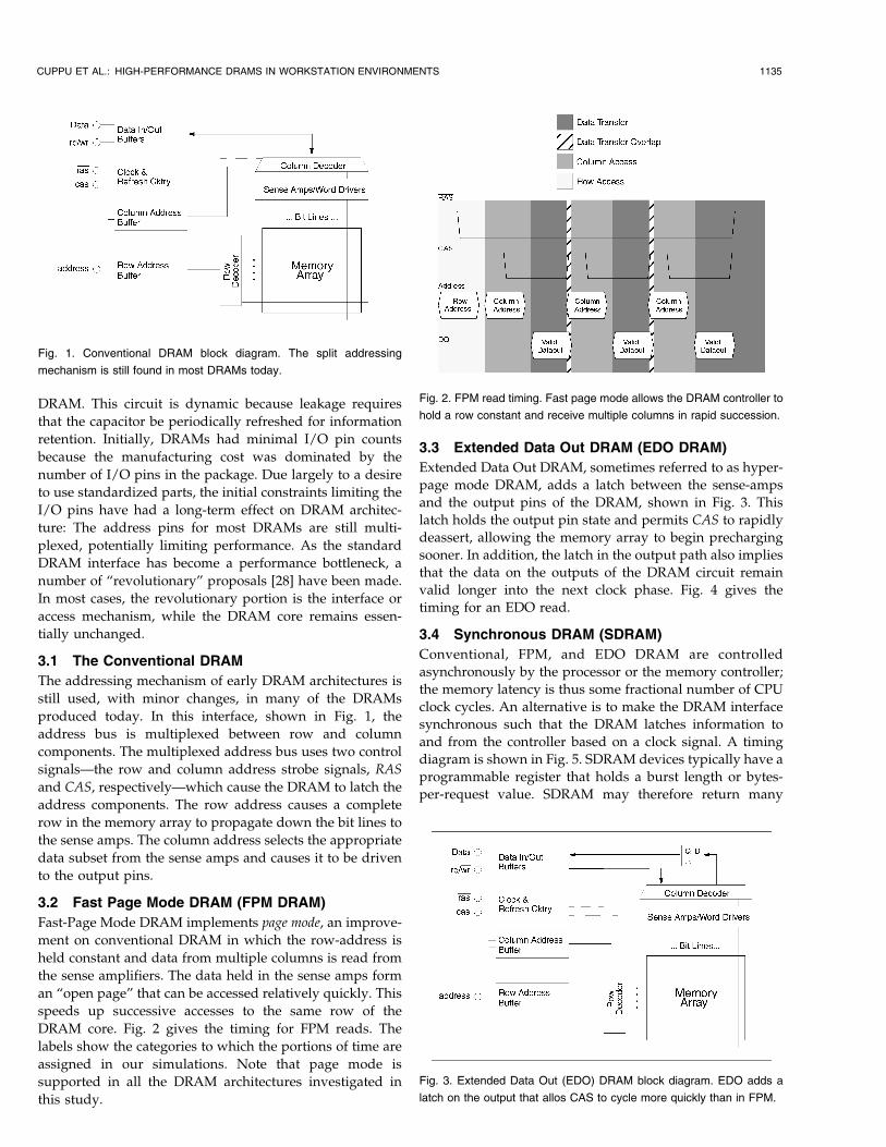
3.1 The Conventional DRAM
The addressing mechanism of early DRAM architectures is
still used, with minor changes, in many of the DRAMs
produced today. In this interface, shown in Fig. 1, the
address bus is multiplexed between row and column
components. The multiplexed address bus uses two control
signalsÐthe row and column address strobe signals, RAS
and CAS, respectivelyÐwhich cause the DRAM to latch the
address components. The row address causes a complete
row in the memory array to propagate down the bit lines to
the sense amps. The column address selects the appropriate
data subset from the sense amps and causes it to be driven
to the output pins.
3.2 Fast Page Mode DRAM (FPM DRAM)
Fast-Page Mode DRAM implements page mode, an improve-
ment on conventional DRAM in which the row-address is
held constant and data from multiple columns is read from
the sense amplifiers. The data held in the sense amps form
an ªopen pageº that can be accessed relatively quickly. This
speeds up successive accesses to the same row of the
DRAM core. Fig. 2 gives the timing for FPM reads. The
labels show the categories to which the portions of time are
assigned in our simulations. Note that page mode is
supported in all the DRAM architectures investigated in
this study.
3.3 Extended Data Out DRAM (EDO DRAM)
Extended Data Out DRAM, sometimes referred to as hyper-
page mode DRAM, adds a latch between the sense-amps
and the output pins of the DRAM, shown in Fig. 3. This
latch holds the output pin state and permits CAS to rapidly
deassert, allowing the memory array to begin precharging
sooner. In addition, the latch in the output path also implies
that the data on the outputs of the DRAM circuit remain
valid longer into the next clock phase. Fig. 4 gives the
timing for an EDO read.
3.4 Synchronous DRAM (SDRAM)
Conventional, FPM, and EDO DRAM are controlled
asynchronously by the processor or the memory controller;
the memory latency is thus some fractional number of CPU
clock cycles. An alternative is to make the DRAM interface
synchronous such that the DRAM latches information to
and from the controller based on a clock signal. A timing
diagram is shown in Fig. 5. SDRAM devices typically have a
programmable register that holds a burst length or bytes-
per-request value. SDRAM may therefore return many
CUPPU ET AL.: HIGH-PERFORMANCE DRAMS IN WORKSTATION ENVIRONMENTS 1135
Fig. 1. Conventional DRAM block diagram. The split addressing
mechanism is still found in most DRAMs today.
Fig. 2. FPM read timing. Fast page mode allows the DRAM controller to
hold a row constant and receive multiple columns in rapid succession.
Fig. 3. Extended Data Out (EDO) DRAM block diagram. EDO adds a
latch on the output that allos CAS to cycle more quickly than in FPM.

bytes over several cycles per request. The advantagesinclude the elimination of the timing strobes and theavailability of data from the DRAM each clock cycle. Theunderlying architecture of the SDRAM core is the same asin a conventional DRAM.
3.5 Enhanced Synchronous DRAM (ESDRAM)
Enhanced Synchronous DRAM is a modification to Syn-chronous DRAM that parallels the differences between FPMand EDO DRAM. First, the internal timing parameters ofthe ESDRAM core are faster than SDRAM. Second, SRAMrow-caches have been added at the sense-amps of eachbank. These caches provide the kind of improved inter-rowperformance observed with EDO DRAM, allowing requeststo the last accessed row to be satisfied even whensubsequent refreshes, precharges, or activates are takingplace. It also allows a write to proceed through the senseamps directly without overwriting the line buffered in theSRAM cache, which would otherwise destroy any readlocality.
3.6 Double Data Rate DRAM (DDR DRAM)
Double data rate (DDR) DRAM doubles the bandwidthavailable from SDRAM by transferring data at both edges ofthe clock. DDR DRAM are very similar to single data rateSDRAM in all other characteristics. They use the samesignaling technology, the same interface specification, andthe same pinouts on the DIMM carriers. However,
DDR-DRAM's internal transfers from and to the DRAMarray, respectively, read and write twice the number of bitsas SDRAM.
3.7 Synchronous Link DRAM (SLDRAM)
RamLink is the IEEE standard (P1596.4) for a busarchitecture for devices. Synchronous Link (SLDRAM) isan adaptation of RamLink for DRAM and is another IEEEstandard (P1596.7). Both are adaptations of the ScalableCoherent Interface (SCI). The SLDRAM specification istherefore an open standard allowing for use by vendorswithout licensing fees. SLDRAM uses a packet-based splitrequest/response protocol. Its bus interface is designed torun at clock speeds of 200-600 MHz and has a two-byte-wide datapath. SLDRAM supports multiple concurrenttransactions, provided all transactions reference uniqueinternal banks. The 64Mbit SLDRAM devices contain eightbanks per device.
Note that SLDRAM is currently only of academicinterest; the SLDRAM standards development effort hasrecently been abandoned, and it is unlikely that anySLDRAM chips will ever be produced.
3.8 Rambus DRAMs (RDRAM)
Rambus DRAMs use a one-byte-wide multiplexed address/data bus to connect the memory controller to the RDRAMdevices. The bus runs at 300 Mhz and transfers on bothclock edges to achieve a theoretical peak of 600 Mbytes/s.Physically, each 64-Mbit RDRAM is divided into fourbanks, each with its own row buffer, and, hence, up to fourrows remain active or open.1 Transactions occur on the bususing a split request/response protocol. Because the bus ismultiplexed between address and data, only one transac-tion may use the bus during any four clock cycle period,referred to as an octcycle. The protocol uses packettransactions; first, an address packet is driven, then thedata. Different transactions can require different numbers ofoctcycles, depending on the transaction type, location of thedata within the device, number of devices on the channel,etc. Fig. 6 gives a timing diagram for a read transaction.
3.9 Direct Rambus (DRDRAM)
Direct Rambus DRAMs use a 400 Mhz 3-byte-widechannel (two for data, one for addresses/commands).Like the Rambus parts, Direct Rambus parts transfer atboth clock edges, implying a maximum bandwidth of1.6 Gbytes/s. DRDRAMs are divided into 16 banks with17 half-row buffers.2 Each half-row buffer is sharedbetween adjacent banks, which implies that adjacentbanks cannot be active simultaneously. This organizationhas the result of increasing the row-buffer miss rate ascompared to having one open row per bank, but itreduces the cost by reducing the die area occupied by therow buffers, compared to 16 full row buffers. A criticaldifference between RDRAM and DRDRAM is that, becauseDRDRAM partitions the bus into different components,
1136 IEEE TRANSACTIONS ON COMPUTERS, VOL. 50, NO. 11, NOVEMBER 2001
1. In this study, we model 64-Mbit Rambus parts, which have four banksand four open rows. Earlier 16-Mbit Rambus organizations had two banksand two open pages and future 256-Mbit organizations may have evenmore.
2. As with the previous part, we model 64-Mbit Direct Rambus, whichhas this organization. Future (256-Mbit) organizations may look different.
Fig. 4. EDO read timing. The output latch in EDO DRAM allows more
overlap between column access and data transfer than in FPM.
Fig. 5. SDRAM read operation clock diagram. SDRAM contains a
writable register for the request length, allowing high-speed column
access.
three transactions can simultaneously use the differentportions of the DRDRAM interface.
4 EXPERIMENTAL METHODOLOGY
To obtain accurate timing of memory requests in adynamically reordered instruction stream, we integratedour code into SimpleScalar, an execution-driven simulatorof an aggressive out-of-order processor [4]. We calculate theDRAM access time, much of which is overlapped withinstruction execution. To determine the degree of overlap,and to separate memory stalls due to bandwidth limitationsfrom memory stalls due to latency limitations, we run twoother simulationsÐone with perfect primary memory (zeroaccess time) and one with a perfect bus (as wide as an L2cache line). Following the methodology in [5], we partitionthe total application execution time into three components,TP, TL, and TB, which correspond, respectively, to timespent processing, time spent stalling for memory due tolatency, and time spent stalling for memory due to limitedbandwidth. In this paper, time spent ªprocessingº includesall activity above the primary memory system, i.e., itcontains all processor execution time and L1 and L2 cacheactivity. Let TR be the total execution time for the realisticsimulation; let TU be the execution time assuming un-limited bandwidthÐthe results from the simulation thatmodels cacheline-wide buses. Then TP is the time given bythe simulation that models a perfect primary memorysystem, and we can calculate TL and TB as follows: TL �TU ÿ TP and TB � TR ÿ TU. In addition, we consider the
degree to which the processor is successful in overlappingmemory access time with processing time. We call theoverlap component TO, and, if TM is the total time spent inthe primary memory system (the time returned by ourDRAM simulator), then TO � TP ÿ �TR ÿ TM�. This is theportion of TP that is overlapped with memory access.
4.1 DRAM Simulator Overview
The DRAM simulator models the internal state of thefollowing DRAM architectures: Fast Page Mode [36],Extended Data Out [19], Synchronous [20], EnhancedSynchronous [13], [20], Double Data Rate [21], SynchronousLink [38], Rambus [32], and Direct Rambus [33].
The timing parameters for the different DRAM archi-tectures are given in Table 1. Since we could not find a64M-bit part specification for ESDRAM, we extrapolatedbased on the most recent SDRAM and ESDRAM datasheets.To measure DRAM behavior in systems of differingperformance, we varied the speed at which requests arriveat the DRAM. We ran the L2 cache at speeds of 100ns, 10ns,and 1ns, and, for each L2 access-time, we scaled the mainprocessor's speed accordingly (the CPU runs at 10x the L2cache speed).
We wanted a model of a typical workstation, so theprocessor is eight-way superscalar, out-of-order, with lock-up-free L1 caches. L1 caches are split 64KB/64KB, 2-way setassociative, with 64-byte linesizes. The L2 cache is unified1MB, 4-way set associative, writeback, and has a 128-bytelinesize. The L2 cache is lockup-free, but only allows oneoutstanding DRAM request at a time; note this organizationfails to take advantage of some of the newer DRAM partsthat can handle multiple concurrent requests. This isaddressed later on in the discussion and in several follow-on studies of ours [7], [8], [11]. 100MHz 128-bit buses arecommon for high-end workstations, so this is the busconfiguration that we model. Note that it also has the samebandwidth as Direct Rambus (1.6 GB/s). We assume thatthe communication overhead is only one 10ns cycle in eachdirection. For the DDR simulations, the bus transfers dataon both edges of the clock; therefore, its effective bandwidthis twice that of the other simulations. See Table 2.
The DRAM/bus configurations simulated are shown inFig. 7. For DRAMs other than Rambus and SLDRAM, eightDRAMs are arranged in parallel in a DIMM-like organiza-tion to obtain a 128-bit bus. SLDRAM, RDRAM, and
CUPPU ET AL.: HIGH-PERFORMANCE DRAMS IN WORKSTATION ENVIRONMENTS 1137
Fig. 6. Rambus DRAM read operation. Rambus DRMs transfer on both
edges of a fast clock and can handle multiple simultaneous requests.
TABLE 1DRAM Specifications Used in Simulations
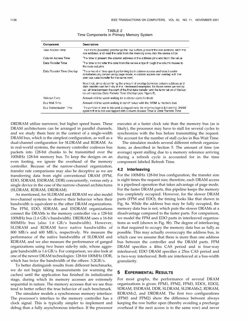
DRDRAM utilize narrower, but higher speed buses. TheseDRAM architectures can be arranged in parallel channels,and we study them here in the context of a single-widthDRAM bus, which is the simplest configuration, as well as adual-channel configuration for SLDRAM and RDRAM. Asin real-world systems, the memory controller coalesces buspackets into 128-bit chunks to be transmitted over the100MHz 128-bit memory bus. To keep the designs on aneven footing, we ignore the overhead of the memorycontroller. Because of the narrow-channel organization,transfer rate comparisons may also be deceptive as we aretransferring data from eight conventional DRAM (FPM,EDO, SDRAM, ESDRAM, DDR) concurrently, versus only asingle device in the case of the narrow-channel architectures(SLDRAM, RDRAM, DRDRAM).
As mentioned, for SLDRAM and RDRAM we also modeltwo-channel systems to observe their behavior when theirbandwidth is equivalent to the other DRAM organizations.The FPM, EDO, SDRAM, and ESDRAM organizationsconnect the DRAMs to the memory controller via a 128-bit100MHz bus (1.6 GB/s bandwidth). DRDRAM uses a 16-bit800MHz bus (also 1.6 GB/s bandwidth). However,SLDRAM and RDRAM have native bandwidths of800 MB/s and 600 MB/s, respectively. We measure theperformance of the native bandwidths of SLDRAM andRDRAM, and we also measure the performance of gangedorganizations using two buses side-by side, whose aggre-gate bandwidth is 1.6 GB/s. For comparison, we also look atone of the newer DRAM technologies: 128-bit 100MHz DDR,which has twice the bandwidth of the others: 3.2GB/s.
To better distinguish results from different benchmarks,we do not begin taking measurements (or warming thecaches) until the application has finished its initializationstage, during which its memory accesses are extremelysequential in nature. The memory accesses that we see thustend to better reflect the true behavior of each benchmark.
The simulator models a synchronous memory interface:The processor's interface to the memory controller has aclock signal. This is typically simpler to implement anddebug than a fully asynchronous interface. If the processor
executes at a faster clock rate than the memory bus (as islikely), the processor may have to stall for several cycles tosynchronize with the bus before transmitting the request.We account for the number of stall cycles in Bus Wait Time.
The simulator models several different refresh organiza-tions, as described in Section 5. The amount of time (onaverage) spent stalling due to a memory reference arrivingduring a refresh cycle is accounted for in the timecomponent labeled Refresh Time.
4.2 Interleaving
For the 100MHz 128-bit bus configuration, the transfer sizeis eight times the request size; therefore, each DRAM accessis a pipelined operation that takes advantage of page mode.For the faster DRAM parts, this pipeline keeps the memorybus completely occupied. However, for the slower DRAMparts (FPM and EDO), the timing looks like that shown inFig. 8a. While the address bus may be fully occupied, thememory data bus is not, which puts the slower DRAMs at adisadvantage compared to the faster parts. For comparison,we model the FPM and EDO parts in interleaved organiza-tions as well (shown in Fig. 8b). The degree of interleavingis that required to occupy the memory data bus as fully aspossible. This may actually overoccupy the address bus, inwhich case we assume that there is more than one addressbus between the controller and the DRAM parts. FPMDRAM specifies a 40ns CAS period and is four-wayinterleaved; EDO DRAM specifies a 25ns CAS period andis two-way interleaved. Both are interleaved at a bus-widthgranularity.
5 EXPERIMENTAL RESULTS
For most graphs, the performance of several DRAMorganizations is given: FPM1, FPM2, FPM3, EDO1, EDO2,SDRAM, ESDRAM, DDR, SLDRAM, SLDRAMx2, RDRAM,RDRAMx2, and DRDRAM. The first two configurations(FPM1 and FPM2) show the difference between alwayskeeping the row buffer open (thereby avoiding a prechargeoverhead if the next access is to the same row) and never
1138 IEEE TRANSACTIONS ON COMPUTERS, VOL. 50, NO. 11, NOVEMBER 2001
TABLE 2Time Components in Primary Memory System

keeping the row buffer open. FPM1 is the pessimistic
strategy of closing the row buffer after every access and
precharging immediately; FPM2 is the optimistic strategy
of keeping the row buffer open and delaying precharge.
The difference is seen in Row Access Time, which, as the
graphs show, is not large for present-day organizations.
For all other DRAM simulations but ESDRAM, we keep
the row buffer open as the timing of the pessimistic
strategy can be calculated without simulation. The FPM3
and EDO2 labels represent the interleaved organizations
of FPM and EDO DRAM. The SLDRAMx2 and
RDRAMx2 labels represent the SLDRAM and RDRAM
organizations with two channels (described earlier). The
remaining labels should be self-explanatory.
5.1 Handling Refresh
Surprisingly, DRAM refresh organization can affect perfor-mance dramatically. Where the refresh organization is notspecified for an architecture, we simulate a model in whichthe DRAM allocates bandwidth to either memory referencesor refresh operations at the expense of predictability [28].The refresh period for all DRAM parts but Rambus is 64ms;Rambus parts have a refresh period of 33ms. In thesimulations presented in this paper, this period is dividedinto N individual refresh operations that occur33/N milliseconds apart, where 33 is the refresh period inmilliseconds, and N is the number of rows in an internalbank times the number of internal banks. This is theRambus mechanism and a memory request can be delayedat most the refresh of one DRAM row. For Rambus parts,this behavior is spelled out in the data sheets. For otherDRAMs, the refresh mechanism is not explicitly stated.Note that, normally, when multiple DRAMs are gangedtogether into physical banks, all banks are refreshed at thesame time. This is different; Rambus refreshes internalbanks individually.
Because many textbooks describe the refresh operationas a periodic shutting down of the DRAM until all rows arerefreshed (e.g., [17]), we also simulated stalling the DRAMonce every 64ms to refresh the entire memory array; thus,every 64ms, one can potentially delay one or more memoryreferences for the length of time it takes to refresh the entirememory array. This approach yields refresh stalls up to twoorders of magnitude worse than the time-interspersedscheme. Particularly hard-hit was the compress benchmark,
CUPPU ET AL.: HIGH-PERFORMANCE DRAMS IN WORKSTATION ENVIRONMENTS 1139
Fig. 7. DRAM bus configurations. The DRAM/bus organizations used in(a) in noninterleaved FPM, EDO, SDRAM, and ESDRAM simulations,(b) the SLDRAM and Rambus simulations, (c) the SLDRAM andRambus dual-channel organizations, and (d) the parallel-channelSLDRAM and Rambus performance numbers in Fig. 11. Due todifferences in bus design, the only bus overhead included in thesimulations is that of the bus that is common to all organizations: the100MHz 128-bit memory bus.
Fig. 8. Interleaving in DRAM simulator. Time in Data Transfer Overlapaccounts for much activity in interleaved organizations. Bus Transmis-sion is the remainder of time that is not overlapped with anything else.(a) Noninterleaved timing for access to DRAM. (b) Interleaved timing foraccess to DRAM.

shown in Fig. 9, with refresh stalls accounting for over 50percent of the average access time in several of the DRAMarchitectures. Because such high overheads are easilyavoided with an appropriate refresh organization, we onlypresent results for the time-interspersed refresh approach.
5.2 Total Execution Time
Fig. 10a shows the total execution time for several bench-marks of SPECint '953 using SDRAM for the primarymemory system. The time is divided into processorcomputation, which includes accesses to the L1 and L2caches, and time spent in the primary memory system. Thegraphs also show the overlap between processor computa-tion and DRAM access time. For each architecture, there arethree vertical bars, representing L2 cache cycle times of100ns, 10ns, and 1ns (left, middle, and rightmost bars,respectively). For each DRAM architecture and L2 cacheaccess time, the figure shows a bar representing executiontime, partitioned into four components:
. memory stall cycles due to limited bandwidth,
. memory stall cycles due to latency,
. processor time (includes L1 and L2 activity) that isoverlapped with memory access,
. processor time (includes L1 and L2 activity) that isnot overlapped with memory access.
One of the most obvious results is that more than half of theSPECint '95 benchmarks (gcc, ijpeg, m88ksim, perl, andvortex) exhibit the same memory-system overhead that hasbeen reported in the literature for large-footprint applica-tions considered much more memory-intensive than SPEC:The middle bars in Fig. 10a for these benchmarks, whichrepresent CPU speeds of 1GHz, have nonoverlappedDRAM components constituting 10-25 percent of the totalexecution time. This echoes published results for DRAMoverheads in commercial workloads such as transactionprocessing [1], [2], [10], [22].
Another obvious point is that anywhere from 5 percentto 99 percent of the memory overhead is overlapped withprocessor executionÐthe most memory-intensive applica-
tions successfully overlap 5-20 percent. SimpleScalar sche-dules instructions extremely aggressively and hides a fairamount of the memory latency with other workÐthoughthis ªother workº is not all useful work as it includes all L1and L2 cache activity. For the 100ns L2 (corresponding to a100MHz processor), between 50 percent and 99 percent ofthe memory access-time is hidden, depending on the typeof DRAM the CPU is attached to (the faster DRAM partsallow a processor to exploit greater degrees of concurrency).For 10ns (corresponding to a 1GHz processor), between5 percent and 90 percent of the latency is hidden. Asexpected, the slower systems hide more of the DRAMaccess time than the faster systems.
Fig. 10b and Fig. 10c show that the more advancedDRAM designs have reduced the proportion of overheadattributed to limited bandwidth by roughly a factor of three:e.g., looking at the 10ns bars (corresponding to 10GHzCPUs) for both GCC and PERL benchmarks, the Stalls Dueto Memory Bandwidth component decreases from 3 for PERLand 1.5 for GCC in the FPMDRAM organization to 1 forPERL and 0.5 for GCC in the SDRAM, ESDRAM, DDR, andDRDRAM organizations.
The figures also show the difference in performance dueto DRAM architectures. For today's high-end DRAMs (e.g.,SDRAM, Direct Rambus, ESDRAM, and DDR), there is littledifference in total execution time. The rankings do notchange from application to application (DDR is fastest,followed by ESDRAM, Direct Rambus, ad SDRAM), and thegap between the fastest and slowest architectures is only10-15 percent.
Summary. The graphs demonstrate the degree to whichcontemporary DRAM designs are addressing the memorybandwidth problem. Popular high-performance techniques,such as lockup-free caches and out-of-order execution,expose memory bandwidth as the bottleneck to improvingsystem performance, i.e., common techniques for improv-ing CPU performance and tolerating memory latency areexacerbating the memory bandwidth problem [5]. Ourresults show that contemporary DRAM architectures areattacking exactly that problem. We see that the most recenttechnologies (SDRAM, ESDRAM, DDR, SLDRAM, andRambus designs) have reduced the stall time due to limitedbandwidth by a factor of two to three, as compared toearlier DRAM architectures. Unfortunately, there are nomatching improvements in memory latency; while thenewest generation of DRAM architectures decreases thecost of limited bandwidth by a factor of three compared tothe previous generation, the cost of stalls due to latency hasremained almost constant.
The graphs also show the expected result that, as L2cache and processor speeds increase, systems are less ableto tolerate memory latency. Accordingly, the remainder ofour study focuses on the components of memory latency.
5.3 Average Memory Latency
Fig. 11 breaks down the memory-system component ofFig. 10. The access times are divided by the number ofaccesses to obtain an average time-per-DRAM-access. Thisis end-to-end latency: the time to complete an entire requestas opposed to critical-word latency. Much of this time isoverlapped with processor execution; the degree of overlap
1140 IEEE TRANSACTIONS ON COMPUTERS, VOL. 50, NO. 11, NOVEMBER 2001
Fig. 9. The penalty for choosing the wrong refresh organization. In some
instances, time waiting for refresh can account for more than 50 percent.
3. We do not look at the floating-point benchmarks here because theirregular access patterns make them easy targets for optimizations such asprefetching and access reordering [24], [25].

depends on the speed of the L2 cache and main CPU. Sincethe variations in performance are not large, we only showbenchmarks that vary most widely. The differences arealmost entirely due to Row Access Time and Bus Transmission
Time.Row Access Time varies with the hit rate in the row
buffers, which, as later graphs show, is as application-dependent as cache hit-rate. The pessimistic FPM1 strategyof always closing pages wins out over the optimistic FPM2strategy. However, with larger caches, we have seen manyinstances where the open-page strategy wins; compulsoryDRAM accesses tend to exhibit good locality.
The differences between benchmarks in Bus Transmission
Time are due to write traffic. Writes allow a different degreeof overlap between the column access, data transfer, andbus transmission. The heavier the write traffic, the higherthe Bus Transmission component. One can conclude that perl
and compress have heavier write traffic than go or li.Though it is a completely unbalanced design, we also
measured latencies for 128-bit wide configurations forRambus and SLDRAM designs, pictured in Fig. 7d. These
ªparallel-channelº results are intended to demonstrate themismatch between today's bus speeds and fastest DRAMs;they are shown in the bottom left corner of Fig. 11.
Bus Transmission Time is that portion of the bus activitynot overlapped with column access or data transfer, and itaccounts for 10 to 30 percent of the total latency. In the DDRresults, Bus Transmission accounts for 40-45 percent of thetotal, and, in the parallel-channel results, it accounts formore than 50 percent. This suggests that, for some DRAMarchitectures, bus speed is becoming a critical issue. Whilecurrent technologies seem balanced, bus speed is likely tobecome a significant problem very quickly for next-generation DRAMs. It is interesting to note that the recentlyannounced Alpha 21364 integrates Rambus memory con-trollers onto the CPU and connects the processor directly tothe DRDRAMs with a 400MHz Rambus Channel, therebyeliminating the slow intermediate bus [16].
EDO DRAM does a much better job than FPM DRAM ofoverlapping column access with data transfer. This is to beexpected, given the timing diagrams for these architectures.Note that the overlap components (Data Transfer Time
CUPPU ET AL.: HIGH-PERFORMANCE DRAMS IN WORKSTATION ENVIRONMENTS 1141
Fig. 10. Total execution time + access time to the primary memory system. (a) shows the total execution time in CPI for all benchmarks, usingSynchronous DRAM. (b) and (c) give total execution time in units of CPI for different DRAM types ((b) for gcc, (c) for perl). The overhead is brokeninto processor time and memory time, with overlap between the two shown and memory cycles are divided into those due to limited bandwidth andthose due to latency.

Overlap) tend to be very large in general, demonstrating
relatively significant performance savings due to page-
mode. This is an argument for keeping buses no wider than
half the block size of the L2 cache.Several of the architectures show no overlap at all
between data transfer and column access. SDRAM and
ESDRAM do not allow such overlap because they instead
use burst mode, which obviates multiple column accesses
(see Fig. 5). SLDRAM does allow overlap, just as the
Rambus parts do; however, for simplicity, in our simula-
tions, we modeled SLDRAM's burst mode. The overlapped
mode would have yielded similar latencies.The interleaved configurations (FPM3 and EDO2) de-
monstrate excellent performance; latency for FPM DRAM
improves by a factor of 2 with four-way interleaving, and
EDO improves by 25-30 percent with two-way interleaving.
1142 IEEE TRANSACTIONS ON COMPUTERS, VOL. 50, NO. 11, NOVEMBER 2001
Fig. 11. Break-downs for primary memory access time, 128-bit bus. These graphs present the average access time on a 128-bit bus across DRAMarchitectures for benchmarks that display the most widely varying behavior. The different DRAM architectures display significantly different accesstimes. The main cause for variation from benchmark to benchmark is the Row-Access Time, which varies with the probability of hitting an open pagein the DRAM's row buffers. If a benchmark exhibits a high degree of locality in its post-L2 address stream, it will tend to have a small Row AccessTime component.

The interleaved EDO configuration performs slightly worsethan the FPM configuration because it does not take fulladvantage of the memory bus; there is still a small amountof unused data bus bandwidth. Note that the break-downsof these organizations look very much like Direct Rambus;Rambus behaves similarly to highly interleaved systems butat much lower cost points.
The ªx2º variants of SLDRAM and RDRAM demonstrateexcellent performance as well. Both Column Access and DataTransfer decrease by a factor of two; both channels can beactive simultaneously, fetching or writing different parts ofthe same L2 cache line. This behavior is expected. Thisreduces the average DRAM access time by roughly30 percent and the total execution time (see Fig. 10) by25 percent, making these configurations as fast as any otherof the modern DRAM designs.
The time stalled due to refresh tends to account for1-2 percent of the total latency; this is more in line withexpectations than the results shown in Fig. 9. The timestalled synchronizing with the memory bus is in the samerange, accounting for 1-5 percent of the total. This is a smallprice to pay for a simpler DRAM interface, compared to afully asynchronous design.
Summary. The FPM architecture is the baseline archi-tecture, but it could be sped up by 30 percent with a greaterdegree of overlap between the column access and datatransmission. This is seen in the EDO architecture: Itscolumn access is a bit faster due to the latch between thesense amps and the output pins, and its degree of overlapwith data transfer is greater, yielding a significantly fasterdesign using essentially the same technology as FPM.Synchronous DRAM is another 30 percent faster than EDO,and Enhanced SDRAM increases performance another15 percent by improving the row- and column-accesstiming parameters and adding an SRAM cache to improveconcurrency. DDR is the fastest of the DRAM architecturesstudied, which is not surprising due to its bandwidth,which is twice that of the other DRAMs studied. It isinteresting to note that its performance is slightly betterthan that of Enhanced Memory's SDRAM, and Fig. 10shows that, while it has reduced the bandwidth portion oflatency more than ESDRAM, ESDRAM has reduced thelatency component more than DDR. This is to be expectedas DDR has a core that is fundamentally similar to that ofSDRAMÐit simply has a faster interfaceÐwhile ESDRAMhas a core unlike any other DRAM architecture studied:Latching the entire row optimally hides the prechargeactivity and increases the overlap between access todifferent rows, thus reducing average latency.
As modeled, SLDRAM and Rambus designs have higherend-to-end transaction latencies than SDRAM, ESDRAM, orDDR, as they require twice as many data transfers tocomplete a 128-bit transaction. However, they are notganged together into a wide datapath as are the otherorganizations. Despite the handicap, SLDRAM performswell, which is important considering it is a public standard.The SLDRAMx2 and RDRAMx2 variants, which have thesame bandwidth and therefore the same number of datatransfers as the other organizations, manage to make up thedifference in performance, with SLDRAMx2 yielding the
same performance as Direct Rambus. Direct Rambus alsocomes out about equal to SDRAM in end-to-end latency anda little behind ESDRAM and DDR.
Last, the DDR results and parallel-channel resultsdemonstrate the failure of a 100MHz 128-bit bus to keepup with today's fastest parts. DDR spends more than40 percent of its time in bus transmissionÐsometimes asmuch as twice the overhead as other DRAMs, suggestingthat the bus is not keeping up with the speed of the DDRDRAM core. In the parallel-channel organizations, wehave placed enough narrow channels side-by-side tocreate a 128-bit datapath that is then pushed across the100MHz bus; even with the increased bandwidth, DirectRambus has roughly the same end-to-end latency asbefore. Both these results suggest that we are pushing thelimits of today's buses. The Alpha 21364 will solve thisproblem by ganging together multiple Rambus Channelsconnected directly to the CPU, eliminating the 100MHzbus [16].
5.4 Perfect-Width Buses
As a limit study, we measured the performance of a perfect-width bus: 100MHz and as wide as an L2 cache line. Theresults are shown in Fig. 12. The scale is much smaller thanthe previous graphs, and some, but not all, of thecomponents have scaled with the change in bus width.The number of column accesses is reduced by a factor ofeight, which reduces the Column Access and Data Transfertimes. The row access remains the same, as does Bus WaitTime; they appear to have increased in importance. Bustransmission for a read has been reduced from 90ns (10 forthe request, 80 to transmit the data), much of which wasoverlapped with column access and data transfer, to 20ns,none of which is overlapped. Because each request requiresonly one memory access, there is no pipelining to beexploited, and the full 20ns transmission is exposed (10nseach for address and data). FPM2 and FPM3 look identical,as do EDO1 and EDO2. This is no mistake. Two configura-tions are interleaved; the others are not. Making the bus thewidth of the request size obviates interleaving.
The fastest of the designs is ESDRAM, not DDR as onewould expect based on the average access-time graphs. Asmentioned earlier, this is because ESDRAM is the onearchitecture studied that has a different internal core; allother DRAMs have the same DRAM core inside. DDRtherefore only has a bandwidth advantage over othersÐanadvantage that is nullified when modeling a perfect-widthbus. This figure thus serves to highlight the time-to-first-bitinefficiencies of the various DRAM interfaces.
There are no Overlap components in these graphs. With a128-byte bus, each cache line fill requires a single transac-tion. Overlap is possible if multiple concurrent requests tothe DRAM are allowed, but this is beyond the scope of ourcurrent DRAM simulations. Overlap shown in previousgraphs is due to the overlap of multiple requests requiredfor a single cache line fill.
As before, the primary variation between benchmarks isthe Row Access Time. The variations are larger than in theprevious graphs because the row access time is proportion-ally much larger. The graphs show that the locality ofreference for each application (seen in the row-buffer hit-
CUPPU ET AL.: HIGH-PERFORMANCE DRAMS IN WORKSTATION ENVIRONMENTS 1143

rates, Fig. 19) can have a dramatic impact on the access
latencyÐfor example, there is a 10 to 90 percent difference
between the average access latencies for li and perl. This
effect has been seen beforeÐMcKee et al.'s work shows that
intentionally reordering memory accesses to exploit locality
can have an order of magnitude effect on memory-system
performance [24], [25].Summary. Coupled with extremely wide buses that hide
the effects of limited bandwidth and thus highlight the
differences in memory latency, the DRAM architectures
perform similarly. As FPM1 and ESDRAM show, the
variations in Row Access can be avoided by always closing
the row buffer after an access and hiding the sense-amp
precharge time during idle moments. This yields the best
measured performance, and its performance is much more
deterministic (e.g., FPM1 yields the same Row Access,
independent of benchmark). Note that, in studies with a
4MB L2 cache, some benchmarks executing with an
optimistic strategy showed very high row-buffer hit rates
and had Row Access components that were near-zero (see
Fig. 13); however, this simply serves to illustrate the
behavior when the bulk of the requests reaching the DRAM
system are compulsory cache misses.Comparing the 128-byte results to the previous experi-
ment, we see that, when one considers current technology
(128-bit buses), there is little variation from application to
application in the average memory access time. The two
components that vary, Row Access and Bus Transmission,
contribute little to the total latency, being overshadowed by
long memory-access pipelines that exploit page mode.
However, moving to wider buses decreases the column
accesses per request, and, as a result, the row access, which
is much larger than column access to begin with, becomes
significant. With fewer column accesses per request, we are
less able to hide bus transmission time, and this component
becomes more noticeable as well.Variations in row access time, though problematic for
real-time systems, do offer an opportunity to optimize
1144 IEEE TRANSACTIONS ON COMPUTERS, VOL. 50, NO. 11, NOVEMBER 2001
Fig. 12. Break-downs for primary memory access times, 128-byte bus. These graphs present the average access time on a 128-byte bus, the samewidth as an L2 cache line. Therefore, the pipelined access to memory (multiple column accesses per row access) is not seen, and the Row Accesscomponent becomes relatively more significant than in the results of a 128-bit bus (Fig. 11). Whereas, in Fig. 11, variations in Row Access causedoverall variations in access time of roughly 10 percent, these graphs quantify the effect that Row Access has on systems with wider buses; averageaccess time can vary by a factor of two.
performance: One can easily imagine enhanced row-buffercaching schemes, row-buffer victim caches, or even predic-tion mechanisms that attempt to capitalize on the amount ofpost-L2-cache locality. However, with current organiza-tions, such measures make little senseÐfor example, ourrecent comparison of VCRAM and ESDRAM shows littledifference in performance, though VCDRAM expends moredie area in a set-associative organization of the samenumber of SRAM bits on the DRAM die [11].
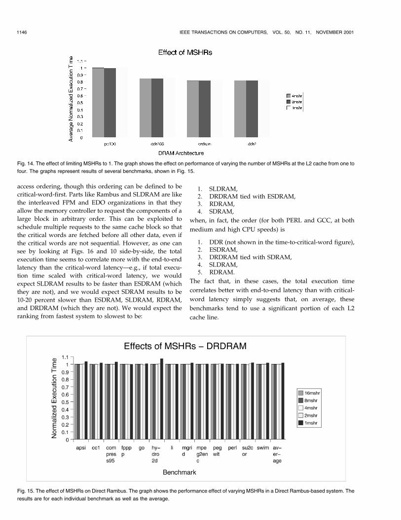
5.5 The Effect of Limited MSHRs
As mentioned in Section 4.1, the measurements presentedso far represent a system model with lock-up free caches,but with what is effectively a single MSHR at the L2-cachelevel. Though there can be up to 32 outstanding missesbetween the L1 and L2 caches, and though the L2 cacheallows any number of hits under a miss, only a single L2miss can be active in the memory system. This fails toexploit the degrees of concurrency offered by highperformance DRAM architecturesÐfor example, DirectRambus can support up to three concurrent accesses.
It is reasonable to wonder how badly this limitationhampers the performance of the DRAMs under study. Toquantify the effect, we present additional data (using adifferent simulator) for the newer DRAM architectures in ahighly concurrent environment in which we vary thenumber of MSHRs. Most of this data, as well as theparticulars of the simulator environment, can be found in[40]. The results in Fig. 14 present data for PC100, DirectRambus DRAM, DDR266, and DDR2 averaged over anumber of benchmarks. The results in Fig. 15 show theindividual benchmarks for DRDRAM alone. Obviously, weexpect little variation from four to 16 MSHRs because thisexceeds the capabilities of single-bus designsÐnonetheless,it acts as a reasonable sanity-check.
As the graphs show, there is, on average, a 1 percentdifference in execution time between a system with a single
MSHR and a system with enough MSHRs to fully occupy aDRAM architecture's abilities. We measured a maximumdifference of roughly 5 percent (shown in the DRDRAMresults). We conclude that our MSHR-based limitation ofconcurreny in the DRAM system introduces no significantperformance degradation. This is not to say that concur-rency in the memory system is not beneficial, however: Welook more closely at the effects of memory-system con-currency in several follow-on studies that suggest con-currency is better exploited at the DRAM-system level thanthe DRAM-architecture level [7], [8].
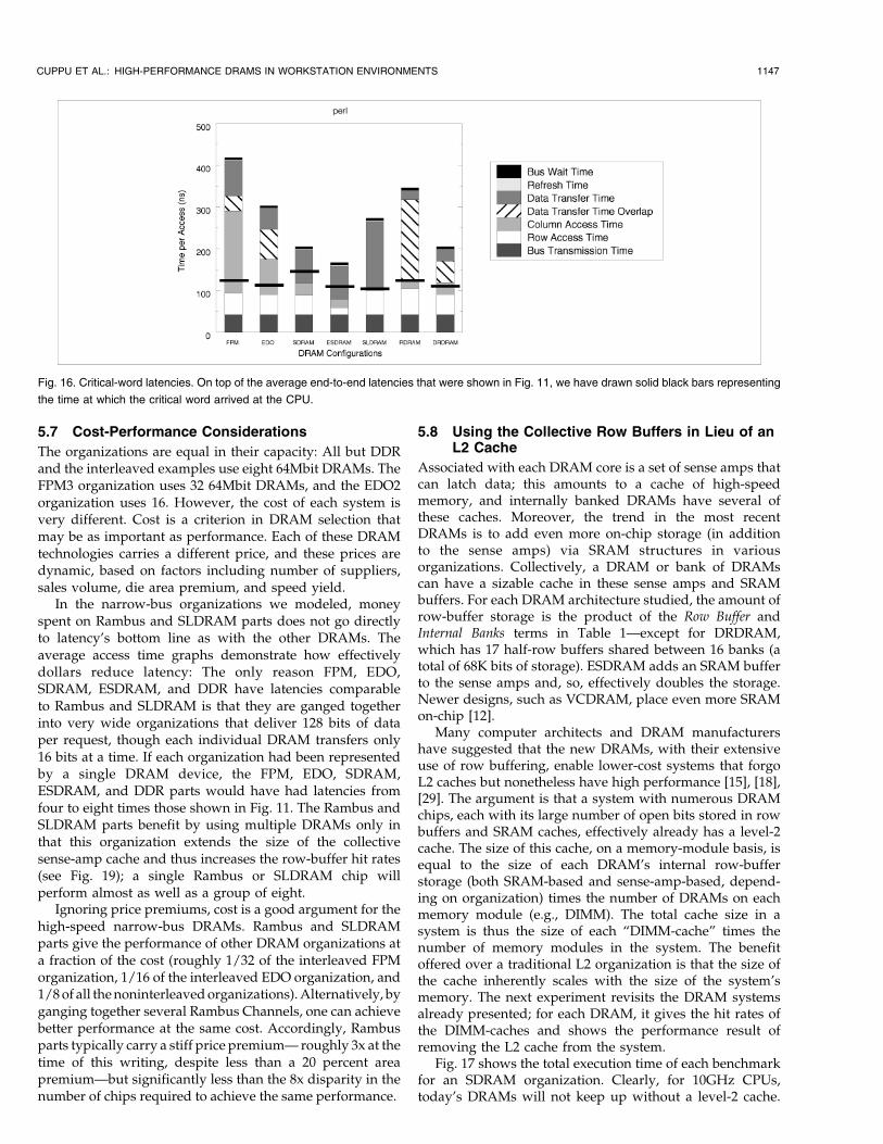
5.6 Critical-Word Latencies
The average access-time numbers shown in Fig. 11represent average end-to-end latency, e.g., for a read, theyrepresent the time from the start of the DRAM request tothe moment the last word in the requested block reaches thelevel-2 cache. This is somewhat misleading because it iswidely held that the true limiter to performance is thecritical-word latency.
Critical-word latencies are shown in Fig. 16 for most ofthe DRAM architectures, at the highest CPU speed. Thefigure shows that time-to-critical-word is significantlylower than the end-to-end latency, as expected. At greatexpense, the end-to-end latency can be improved bywidening the bus, thereby making the end-to-end latencyequal to the critical-word latency. This is shown in Fig. 12(described earlier). Note that doing so yields latenciessimilar to the critical-word latencies in Fig. 16Ðin short,there is no significant latency argument for widening thebus. To reduce latency, one must speed up the bus, speedup the DRAM core, improve the hit ratio in the DRAM rowbuffers, or redesign the DRAM interface.
It is interesting to note that the SLDRAM and Rambusdesigns excel in their ability to schedule the indivisualtransfers in a cache-block request: Though SDRAM andESDRAM win in end-to-end latency, they are rigid in their
CUPPU ET AL.: HIGH-PERFORMANCE DRAMS IN WORKSTATION ENVIRONMENTS 1145
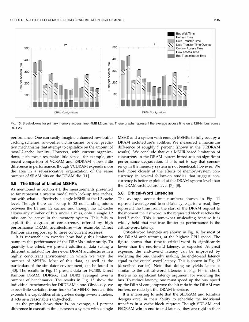
Fig. 13. Break-downs for primary memory access time, 4MB L2 caches. These graphs represent the average access time on a 128-bit bus across
DRAMs.
access ordering, though this ordering can be defined to be
critical-word-first. Parts like Rambus and SLDRAM are like
the interleaved FPM and EDO organizations in that they
allow the memory controller to request the components of a
large block in arbitrary order. This can be exploited to
schedule multiple requests to the same cache block so that
the critical words are fetched before all other data, even if
the critical words are not sequential. However, as one can
see by looking at Figs. 16 and 10 side-by-side, the total
execution time seems to correlate more with the end-to-end
latency than the critical-word latencyÐe.g., if total execu-
tion time scaled with critical-word latency, we would
expect SLDRAM results to be faster than ESDRAM (which
they are not), and we would expect SDRAM results to be
10-20 percent slower than ESDRAM, SLDRAM, RDRAM,
and DRDRAM (which they are not). We would expect the
ranking from fastest system to slowest to be:
1. SLDRAM,2. DRDRAM tied with ESDRAM,3. RDRAM,4. SDRAM,
when, in fact, the order (for both PERL and GCC, at both
medium and high CPU speeds) is
1. DDR (not shown in the time-to-critical-word figure),2. ESDRAM,3. DRDRAM tied with SDRAM,4. SLDRAM,5. RDRAM.
The fact that, in these cases, the total execution time
correlates better with end-to-end latency than with critical-
word latency simply suggests that, on average, these
benchmarks tend to use a significant portion of each L2
cache line.
1146 IEEE TRANSACTIONS ON COMPUTERS, VOL. 50, NO. 11, NOVEMBER 2001
Fig. 15. The effect of MSHRs on Direct Rambus. The graph shows the performance effect of varying MSHRs in a Direct Rambus-based system. The
results are for each individual benchmark as well as the average.
Fig. 14. The effect of limiting MSHRs to 1. The graph shows the effect on performance of varying the number of MSHRs at the L2 cache from one to
four. The graphs represent results of several benchmarks, shown in Fig. 15.
5.7 Cost-Performance Considerations
The organizations are equal in their capacity: All but DDRand the interleaved examples use eight 64Mbit DRAMs. TheFPM3 organization uses 32 64Mbit DRAMs, and the EDO2organization uses 16. However, the cost of each system isvery different. Cost is a criterion in DRAM selection thatmay be as important as performance. Each of these DRAMtechnologies carries a different price, and these prices aredynamic, based on factors including number of suppliers,sales volume, die area premium, and speed yield.
In the narrow-bus organizations we modeled, moneyspent on Rambus and SLDRAM parts does not go directlyto latency's bottom line as with the other DRAMs. Theaverage access time graphs demonstrate how effectivelydollars reduce latency: The only reason FPM, EDO,SDRAM, ESDRAM, and DDR have latencies comparableto Rambus and SLDRAM is that they are ganged togetherinto very wide organizations that deliver 128 bits of dataper request, though each individual DRAM transfers only16 bits at a time. If each organization had been representedby a single DRAM device, the FPM, EDO, SDRAM,ESDRAM, and DDR parts would have had latencies fromfour to eight times those shown in Fig. 11. The Rambus andSLDRAM parts benefit by using multiple DRAMs only inthat this organization extends the size of the collectivesense-amp cache and thus increases the row-buffer hit rates(see Fig. 19); a single Rambus or SLDRAM chip willperform almost as well as a group of eight.
Ignoring price premiums, cost is a good argument for thehigh-speed narrow-bus DRAMs. Rambus and SLDRAMparts give the performance of other DRAM organizations ata fraction of the cost (roughly 1/32 of the interleaved FPMorganization, 1/16 of the interleaved EDO organization, and1/8 of all the noninterleaved organizations). Alternatively, byganging together several Rambus Channels, one can achievebetter performance at the same cost. Accordingly, Rambusparts typically carry a stiff price premiumÐ roughly 3x at thetime of this writing, despite less than a 20 percent areapremiumÐbut significantly less than the 8x disparity in thenumber of chips required to achieve the same performance.
5.8 Using the Collective Row Buffers in Lieu of anL2 Cache
Associated with each DRAM core is a set of sense amps thatcan latch data; this amounts to a cache of high-speedmemory, and internally banked DRAMs have several ofthese caches. Moreover, the trend in the most recentDRAMs is to add even more on-chip storage (in additionto the sense amps) via SRAM structures in variousorganizations. Collectively, a DRAM or bank of DRAMscan have a sizable cache in these sense amps and SRAMbuffers. For each DRAM architecture studied, the amount ofrow-buffer storage is the product of the Row Buffer andInternal Banks terms in Table 1Ðexcept for DRDRAM,which has 17 half-row buffers shared between 16 banks (atotal of 68K bits of storage). ESDRAM adds an SRAM bufferto the sense amps and, so, effectively doubles the storage.Newer designs, such as VCDRAM, place even more SRAMon-chip [12].
Many computer architects and DRAM manufacturershave suggested that the new DRAMs, with their extensiveuse of row buffering, enable lower-cost systems that forgoL2 caches but nonetheless have high performance [15], [18],[29]. The argument is that a system with numerous DRAMchips, each with its large number of open bits stored in rowbuffers and SRAM caches, effectively already has a level-2cache. The size of this cache, on a memory-module basis, isequal to the size of each DRAM's internal row-bufferstorage (both SRAM-based and sense-amp-based, depend-ing on organization) times the number of DRAMs on eachmemory module (e.g., DIMM). The total cache size in asystem is thus the size of each ªDIMM-cacheº times thenumber of memory modules in the system. The benefitoffered over a traditional L2 organization is that the size ofthe cache inherently scales with the size of the system'smemory. The next experiment revisits the DRAM systemsalready presented; for each DRAM, it gives the hit rates ofthe DIMM-caches and shows the performance result ofremoving the L2 cache from the system.
Fig. 17 shows the total execution time of each benchmarkfor an SDRAM organization. Clearly, for 10GHz CPUs,today's DRAMs will not keep up without a level-2 cache.
CUPPU ET AL.: HIGH-PERFORMANCE DRAMS IN WORKSTATION ENVIRONMENTS 1147
Fig. 16. Critical-word latencies. On top of the average end-to-end latencies that were shown in Fig. 11, we have drawn solid black bars representing
the time at which the critical word arrived at the CPU.

However, for the 100MHz and 1GHz CPU speeds (the leftand middle bars in each group of three), we see that thememory component is not overwhelming. With a1GHz CPU and no L2 cache, the DRAM system accountsfor 10-80 percent of the total execution time. For low-costsystems, this might very well be acceptable.
Fig. 18 shows the average access times for both 128-bitbuses and ideal 64-byte buses. The ideal buses are 64 bytesand not 128 bytes because the L1 cache block is 64 bytes.The main result is that these graphs look just like previousgraphs except that the scale is smaller because of thedifference in L1 and L2 block sizes (with the L2 gone, theamount of data per request is cut in half). The most obviousdifference between these results and previous results is thatthere is very little variation from benchmark to benchmark.This is largely because the elimination of the L2 cachemakes write operations more frequent, thereby disruptingread locality [9]. This is also seen in the decreased hit ratesrelative to hit rates with 1MB and 4MB L2 caches (nextfigure).
Fig. 19 presents the variations in hit rates for the row-buffer caches of different DRAM architectures. Hit rate doesnot include the effect of hits that are due to multiplerequests to satisfy one L2 cacheline: These results are for theideal buses. We present results for two sets of benchmarks,including applications from the SPEC and Etch suites. Asmentioned later, the Etch applications are included becausethey tend to have larger footprints than SPEC.
The results show that memory requests frequently hit therow buffers; hit rates range from 2-97 percent, with a meanof 40 percent. Hit rates increase with increasing L2 cachesize (because the DRAM traffic is increasingly compulsorymisses, that tend to be sequential) and decrease as the L2cache disappears (because the writeback L2 does a good jobof filtering out writes, as well as the fact that morenoncompulsory misses will hit the DRAM with the L2cache gone). As shown in our previous study [9], there is asignificant change in hit rate when writes are included inthe address stream: Including write traffic tends to decreasethe row-buffer hit-rate for those DRAMs with less SRAMstorage. Writebacks tend to purge useful data from the
smaller row-buffer caches; thus, the Rambus, SLDRAM,
and ESDRAM parts perform better than the others. This
effect suggests that, when writebacks happen, they do so
without much locality: The cachelines that are written back
tend to be to DRAM pages that have not been accessed
recently. This is expected behavior.Note that a designer can play with the ordering of
address bits to maximize the row-buffer hits. A similar
technique is used in interleaved memory systems to obtain
the highest bandwidth.
5.9 Trace-Driven Simulations
We also investigated the effect of using trace-driven
simulation to measure memory latency. We simulated the
same benchmarks using SimpleScalar's in-order mode with
single-issue. Clearly, in-order execution cannot yield the
same degree of overlap as out-of-order execution, but we
did see virtually identical average access times compared to
out-of-order execution, for both 128-bit and 128-byte buses.
Because SPEC has been criticized as being not representa-
tive of real-world applications, we also used the University
of Washington's Etch traces [14] to corroborate what we had
seen using SPEC on SimpleScalar. The Etch benchmarks
yielded very similar results, with the main difference being
that the row-buffer hit rates had a smaller standard
deviation. An example for the compress benchmark is
shown in Fig. 20; this graph is very representative of the
entire Etch suite. In general, the Etch benchmarks have
similar break-downs, which is expected since their row-
buffer hit rates have a small standard deviation. Also, the
average access times for the Etch benchmarks tend to be
smaller than their SimpleScalar counterparts (see Fig. 11),
and the differences lie primarily in the Bus Transmission
Time component. Trace-driven simulations are often de-
rided for being less accurate; the fact that these results are
so similar to those obtained through accurate request timing
in an out-of-order core suggests that trace-driven ap-
proaches may be viable for future DRAM studies. This is
corroborated by other results of ours [11].
1148 IEEE TRANSACTIONS ON COMPUTERS, VOL. 50, NO. 11, NOVEMBER 2001
Fig. 17. Performance without a level-2 cache.

6 CONCLUSIONS
We have simulated seven commercial DRAM architectures
in a workstation-class setting, connected to a fast, out-of-
order, eight-way superscalar processor with lockup-free
caches. We have found the following:
1. Contemporary DRAM technologies are addressingthe memory bandwidth problem but not thememory latency problem;
2. The memory latency problem is closely tied tocurrent mid- to high-performance memory busspeeds (100MHz), which will soon become inade-quate for high-performance DRAM designs;
3. There is a significant degree of locality in theaddresses that are presented to the primary memorysystemÐthis locality seems to be exploited well byDRAM designs that are multibanked internally andtherefore have more than one row buffer; and
4. Exploiting this locality will become more importantin future systems when memory buses widen,exposing row access time as a significant factor.
The bottom line is that contemporary DRAM architec-
tures have used page-mode and internal interleaving to
achieve a one-time performance boost. These techniques
improve bandwidth directly and improve latency indirectly
by pipelining over the memory bus the multiple transac-
tions that satisfy one read or write request (requests are
often cacheline-sized, and the cache width is typically
greater than the bus width). This is similar to the
performance optimization of placing multiple DRAMs in
parallel to achieve a bus-width datapath: This optimization
works because the bus width is typically greater than an
individual DRAM's transfer width. We have seen that each
of the DRAM architectures studied takes advantage of
internal interleaving and page mode to differing degrees of
success. However, as the studies show, we will soon hit the
limit of these benefits: The limiting factors are now the
speed of the bus and, to a lesser degree, the speed of the
DRAM core. To improve performance further, we must
explore other avenues.
CUPPU ET AL.: HIGH-PERFORMANCE DRAMS IN WORKSTATION ENVIRONMENTS 1149
Fig. 18. Break-downs for primary memory access time, 128-bit and 64-byte bus, no L2 cache. These graphs present the average access time on a
128-bit bus across DRAM architectures for the three benchmarks that display the most widely varying behavior. The different DRAM architectures
display significantly different access times.

7 FUTURE WORK
We will extend the research to cover large systems which
have different performance behavior. In the present study,
the number of DRAMs per organization is small, therefore,
the hit rate seen in the row buffers can be high. In larger
systems, this effect decreases in significance. For instance, in
large systems, bandwidth is more of an issue than latencyÐ
hitting an open page is less important than scheduling the
DRAM requests so as to avoid bus conflicts.We have also extended the work to incorporate higher
degrees of concurrency on the memory bus and additional
experimental DRAM architectures [7], [8], [11].As buses grow wider, Row Access Time becomes sig-
nificant; in our 1MB L2 studies, it accounts for 20-50 percent
of the total latency. Increasing the number of open rows is
1150 IEEE TRANSACTIONS ON COMPUTERS, VOL. 50, NO. 11, NOVEMBER 2001
Fig. 19. Hit-rates in the row buffers. These graphs show hit-rates for the benchmarks on each of the DRAM architectures. The new DRAMs, with
more internal banking, tend to have higher hit rates. Write traffic, due to writebacks, disrupts the locality of the address stream for architectures with
fewer internal banks.
one approach to decreasing the overhead, as seen in themultibanked DRAMs such as Rambus and SLDRAM. Otherapproaches include adding extra row buffers to cachepreviously opened rows, prefetching into the row buffers,placing row-buffer victim-caches onto the chips, predictingwhether or not to close an open page, etc. We intend to lookinto this more closely, but wanted to get a rough idea of thepotential gains. We kept the last eight accessed row buffersin a FIFO and kept track of the number of hits and misses tothe buffer, as well as the depth at which any hits occurred.
The results are shown in Fig. 21. For each benchmark, weshow the number of misses to the main row buffer. Thefirst value at the leftmost of each curve is the number of hitsat a depth of one in the FIFO victim buffer. The next valuerepresents the number of hits at a depth of two and so on.The rightmost value in each curve is the number of accessesthat missed both the main row buffer and the FIFO victimbuffer. The two graphs on the bottom show the amount oflocality in the two benchmarks with the most widelyvarying behavior; the graphs plot the time in CPU clocks
CUPPU ET AL.: HIGH-PERFORMANCE DRAMS IN WORKSTATION ENVIRONMENTS 1151
Fig. 20. Average access times for Etch traces. Results are for 1MB L2 cache and 128-bit buses.
Fig. 21. Locality in the stream of accesses to the single open row in the FPM DRAM. The top six graphs show the frequency with which accesses to a
given DRAM page hit at stack depth x. The bottom two graphs show the interarrival time of accesses that hit in an open DRAM page. Both sets of
graphs show that, when references are made to the data in a particular DRAM page, the accesses tend to be localized in time.

between successive references to the previous open row(i.e., the row that was replaced by the currently open row: italso happens to be the topmost entry in the FIFO). Thisgraph demonstrates that, when the row is accessed in thefuture, it is most often accessed in the very near future. Ourconclusion is that the previously referenced row has a highhit rate and it is likely to be referenced within a short periodof time if it is referenced again at all. A number of proventechniques exist to exploit this behavior, such as victimcaching, set associative row buffers, etc.
ACKNOWLEDGMENTS
This study grew out of research begun by Brian Davis andextended by Vinodh Cuppu, OÈ zkan Dikmen, and RohitGrover in a graduate-level architecture class taught byProfessor Jacob in the spring of 1998. Dikmen and Groverwere instrumental in the development of the simulator usedin this study. The authors would like to thank severalresearchers at IBM who provided helpful insight into theinternal workings of the various DRAM architectures: MarkCharney, Paul Coteus, Phil Emma, Jude Rivers, and JimRogers. They would also like to thank Sally McKee for herdetailed comments on and suggestions for the paper, aswell as the anonymous reviewers of the earlier version ofthis paper that appeared in the Proceedings of theInternational Symposium on Computer Architecture '99(ISCA '99) [9]. Trevor Mudge is supported in part by USDefense Advanced Research Projects Agency grant DABT63-96-C0047. Vinodh Cuppu and Bruce Jacob are supportedin part by US National Science Foundation (NSF) CAREERAward CCR-9983618 and NSF grant EIA-0000439.
REFERENCES
[1] L.A. Barroso, K. Gharachorloo, and E. Bugnion, ªMemory SystemCharacterization of Commercial Workloads,º Proc. 25th Ann. Int'lSymp. Computer Architecture (ISCA'98), pp. 3-14, June 1998.
[2] D. Bhandarkar and J. Ding, ªPerformance Characterization of thePentium Pro Processor,º Proc. Third Int'l Symp. High PerformanceComputer Architecture (HPCA'97), pp. 288-297, Feb. 1997.
[3] N. Bowman, N. Cardwell, C. Kozyrakis, C. Romer, and H. Wang,ªEvaluation of Existing Architectures in IRAM Systems,º Proc.Workshop Mixing Logic and DRAM, June 1997.
[4] D. Burger and T.M. Austin, ªThe SimpleScalar Tool Set, Version2.0,º Technical Report CS-1342, Univ. of Wisconsin-Madison, June1997.
[5] D. Burger, J.R. Goodman, and A. Kagi, ªMemory BandwidthLimitations of Future Microprocessors,º Proc. 23rd Ann. Int'l Symp.Computer Architecture (ISCA '96), pp. 78-89, May 1996.
[6] R. Crisp, ªDirect Rambus Technology: The New Main MemoryStandard,º IEEE Micro, vol. 17, no. 6, pp. 18-28, Nov. 1997.
[7] V. Cuppu and B. Jacob, ªConcurrency, Latency, or SystemOverhead: Which Has the Largest Impact on UniprocessorDRAM-System Performance?º Proc. 28th Int'l Symp. ComputerArchitecture (ISCA '01), June 2001.
[8] V. Cuppu and B. Jacob, ªOrganizational Design Trade-Offs at theDRAM, Memory Bus, and Memory Controller Level: InitialResults,º Technical Report UMD-SCA-1999-2, Univ. of MarylandSystems & Computer Architecture Group, Nov. 1999.
[9] V. Cuppu, B. Jacob, B. Davis, and T. Mudge, ªA PerformanceComparison of Contemporary DRAM Architectures,º Proc. 26thAnn. Int'l Symp. Computer Architecture (ISCA'99), pp. 222-233, May1999.
[10] Z. Cvetanovic and D. Bhandarkar, ªPerformance Characterizationof the Alpha 21164 Microprocessor Using TP and SPEC Work-loads,º Proc. Second Int'l Symp. High Performance ComputerArchitecture (HPCA '96), pp. 270-280, Feb. 1996.
[11] B. Davis, T. Mudge, B. Jacob, and V. Cuppu, ªDDR2 and LowLatency Variants,º Proc. Memory Wall Workshop at the 26th Ann.Int'l Symp. Computer Architecture, May 2000.
[12] B. Dipert, ªThe Slammin, Jammin, DRAM Scramble,º EDN,vol. 2000, no. 2, pp. 68-82, Jan. 2000.
[13] ªESDRAM, Enhanced SDRAM 1M x 16,ºEnhanced MemorySystems, Inc., http://www.edram.com/products/datasheets/16M_esdram0298a.pdf, 1998.
[14] ªEtch: Memory System Research at the University of Washing-ton,º Univ. of Washington, http://etch.cs.washington.edu/, 1998.
[15] J.R. Goodman and M. Chiang, ªThe Use of Static Column RAM asa Memory Hierarchy,º Proc. 11th Ann. Int'l Symp. ComputerArchitecture (ISCA '84), pp. 167-174, June 1984.
[16] L. Gwennap, ªAlpha 21364 to Ease Memory Bottleneck: CompaqWill Add Direct RDRAM to 21264 Core for Late 2000 Shipments,ºMicroprocessor Report, vol. 12, no. 14, pp. 12-15, Oct. 1998.
[17] J.L. Hennessy and D.A. Patterson, Computer Architecture: AQuantitative Approach, second ed. Morgan Kaufmann, 1996.
[18] W.-C. Hsu and J.E. Smith, ªPerformance of Cached DRAMOrganizations in Vector Supercomputers,º Proc. 20th Ann. Int'lSymp. Computer Architecture (ISCA '93), pp. 327-336, May 1993.
[19] IBM, ªEDO DRAM 4M x 16 Part No. IBM0165165PT3C,º IBM,http://www.chips.ibm.com/products/memory/88H2011/88H2011.pdf, 1998.
[20] IBM, ªSDRAM 1M x 16 x 4 Bank Part No. IBM0364164,º IBM,http://www.chips.ibm.com/products/memory/19L3265/19L3265.pdf, 1998.
[21] IBM, ªDDR DRAM 16M x 8 Part No. IBM0612804GT3B,º IBM,http://www.chips.ibm.com/products/memory/06K0566/06K0566.pdf, 2000.
[22] K. Keeton, D.A. Patterson, Y.Q. He, R.C. Raphael, and W.E. Baker,ªPerformance Characterization of a Quad Pentium Pro SMP UsingOLTP Workloads,º Proc. 25th Ann. Int'l Symp. Computer Architec-ture (ISCA '98), pp. 15-26, June 1998.
[23] C. Kozyrakis, S. Perissakis, D. Patterson, T. Anderson, K.Asanovic, N. Cardwell, R. Fromm, J. Golbus, B. Gribstad, K.Keeton, R. Thomas, N. Treuhaft, and K. Yelick, ªScalableProcessors in the Billion-Transistor Era: IRAM,º Computer,vol. 30, no. 9, pp. 75-78, Sept. 1997.
[24] S. McKee, A. Aluwihare, B. Clark, R. Klenke, T. Landon, C. Oliver,M. Salinas, A. Szymkowiak, K. Wright, W. Wulf, and J. Aylor,ªDesign and Evaluation of Dynamic Access Ordering Hardware,ºProc. Int'l Conf. Supercomputing, May 1996.
[25] S.A. McKee and W.A. Wulf, ªAccess Ordering and Memory-Conscious Cache Utilization,º Proc. Int'l Symp. High PerformanceComputer Architecture (HPCA '95), pp. 253-262, Jan. 1995.
[26] B. Nayfeh, L. Hammond, and K. Olukotun, ªEvaluation of DesignAlternatives for a Multiprocessor Microprocessor,º Proc. 23rd Ann.Int'l Symp. Computer Architecture (ISCA '96), pp. 67-77, May 1996.
[27] B.A. Nayfeh, K. Olukotun, and J.P. Singh, ªThe Impact of Shared-Cache Clustering in Small-Scale Shared-Memory Multiproces-sors,º Proc. Second Int'l Symp. High Performance Computer Archi-tecture (HPCA '96), pp. 74-84, Feb. 1996.
[28] S. Przybylski, ªNew DRAM Technologies: A ComprehensiveAnalysis of the New Architectures,º MicroDesign Resources,Sebastopol, Calif., 1996.
[29] Rambus, ªRambus Memory: Enabling Technology for PC Gra-phics,º technical report, Rambus Inc., Mountain View, Calif., Oct.1994.
[30] Rambus, ªComparing RDRAM and SGRAM for 3D Applications,ºtechnical report, Rambus Inc., Mountain View, Calif., Oct. 1996.
[31] Rambus, ªMemory Latency Comparison,º technical report,Rambus Inc., Mountain View, Calif., Sept. 1996.
[32] Rambus, ª16/18Mbit & 64/72Mbit Concurrent RDRAM DataSheet,º Rambus, http://www.rambus.com/docs/Cnctds.pdf,1998.
[33] Rambus, ªDirect RDRAM 64/72-Mbit Data Sheet,º Rambus,http://www.rambus.com/docs/64dDDS.pdf, 1998.
[34] P. Ranganathan, K. Gharachorloo, S.V. Adve, and L.A. Barroso,ªPerformance of Database Workloads on Shared-Memory Systemswith Out-of-Order Processors,º Proc. Eighth Int'l Conf. ArchitecturalSupport for Programming Languages and Operating Systems (ASPLOS'98), pp. 307-318, Oct. 1998.
[35] M. Rosenblum, E. Bugnion, S.A. Herrod, E. Witchel, and A. Gupta,ªThe Impact of Architectural Trends on Operating SystemPerformance,º Proc. 15th ACM Symp. Operating Systems Principles(SOSP '95), Dec. 1995.
1152 IEEE TRANSACTIONS ON COMPUTERS, VOL. 50, NO. 11, NOVEMBER 2001
[36] Samsung, ªFPM DRAM 4M x 16 Part No. KM416V4100C,ºSamsung Semiconductor, http://www.usa.samsungsemi.com/products/prodspec/dramcomp/KM416V40(1)00C.PDF, 1998.
[37] A. Saulsbury, F. Pong, and A. Nowatzyk, ªMissing the MemoryWall: The Case for Processor/Memory Integration,º Proc. 23rdAnn. Int'l Symp. Computer Architecture (ISCA '96), pp. 90-101, May1996.
[38] SLDRAM, ª4M x 18 SLDRAM Advance Datasheet,º SLDRAM,Inc., http://www.sldram.com/Documents/corp400b.pdf, 1998.
[39] R. Wilson, ªMoSys Tries Synthetic SRAM,º EE Times Online, July1997, http://www.eetimes.com/news/98/1017news/tries.html.
[40] B. Davis, ªModern DRAM Architectures,º PhD thesis, Univ. ofMichigan, 2001.
Vinodh Cuppu received the MS degree inelectrical engineering from the University ofMaryland, College Park, in 2000 and the BEdegree in electronics and communication en-gineering from the University of Madras, India, in1997. He is currently a PhD student in theDepartment of Electrical and Computer Engi-neering at the University of Maryland, CollegePark. His research interests include DRAMarchitectures, latency reduction techniques and
power reduction techniques for embedded microprocessors. He is astudent member of the IEEE and the IEEE Computer Society and amember of the ACM.
Bruce Jacob received the AB degree cum laudein mathematics from Harvard University in 1988and the MS and PhD degrees in computerscience and engineering from the University ofMichigan, Ann Arbor, in 1995 and 1997, respec-tively. At the University of Michigan, he was partof a design team building high-performance,high-clock-rate microprocessors. He has alsoworked as a software engineer for two success-ful startup companies: Boston Technology and
Priority Call Management. At Boston Technology, he worked as adistributed systems developer and, at Priority Call Management, he wasthe initial system architect and chief engineer. He is currently on thefaculty of the University of Maryland, College Park, where he is anassistant professor of electrical and computer engineering. His presentresearch covers memory-system design and includes DRAM architec-tures, virtual memory systems, and memory management hardware andsoftware for real-time and embedded systems. He is a recipient of a USNational Science Foundation CAREER award for his work on DRAMsystems. He is a member of the IEEE, the IEEE Computer Society, theACM, and Sigma Xi.
Brian Davis received the BSE degree magnacum laude in electrical engineering from Michi-gan Technological University in 1991 and theMSE and PhD degrees in computer engineeringfrom the University of Michigan, Ann Arbor, in1994 and 2001, respectively. He is presently anassistant professor in the Electrical and Com-puter Engineering Department at MichiganTechnological University. He has served on thefaculty of the University of Toledo and Will-
amette University. His present research is focused upon modern DRAMinterfaces and architectures, latency tolerance in high-speed micro-processors, memory controller policies, and computer simulationmethodologies. Dr. Davis is a member of the IEEE, the IEEE ComputerSociety, the ACM, and Tau Beta Pi.
Trevor Mudge received the BSc degree incybernetics from the University of Reading,England, in 1969 and the MS and PhD degreesin computer science from the University ofIllinois, Urbana, in 1973 and 1977, respectively.Since 1977, he has been on the faculty of theUniversity of Michigan, Ann Arbor. He ispresently a professor of electrical engineeringand computer science and the author of numer-ous papers on computer architecture, program-
ming languages, VLSI design, and computer vision, and he holds apatent in computer-aided design of VLSI circuits. He has also chairedabout 20 theses in these research areas. His research interests includecomputer architecture, computer-aided design, and compilers. Inaddition to his position as a faculty member, he is a on the advisoryboards of for several computer companies and venture funds. Dr.Mudge is a fellow of the IEEE, a member of the ACM, the IEE, and theBritish Computer Society.
. For more information on this or any computing topic, please visitour Digital Library at http://computer.org/publications/dlib.
CUPPU ET AL.: HIGH-PERFORMANCE DRAMS IN WORKSTATION ENVIRONMENTS 1153