high-performance, transparent, and stretchable electrodes ...imdl.khu.ac.kr/publication/2013/161....
TRANSCRIPT
High-Performance, Transparent, and Stretchable Electrodes UsingGraphene−Metal Nanowire Hybrid StructuresMi-Sun Lee,† Kyongsoo Lee,† So-Yun Kim,† Heejoo Lee,† Jihun Park,† Kwang-Hyuk Choi,‡ Han-Ki Kim,‡
Dae-Gon Kim,§ Dae-Young Lee,∥ SungWoo Nam,# and Jang-Ung Park*,†
†School of Nano-Bioscience and Chemical Engineering, School of Mechanical and Advanced Materials Engineering,Low-Dimensional Carbon Materials Center, Ulsan National Institute of Science and Technology (UNIST), Ulsan, 689-798, Republicof Korea‡Department of Advanced Materials Engineering for Information and Electronics, Kyung Hee University, Yongin-si, 446-701,Republic of Korea§Samsung Techwin R&D Center, Seongnam-si, 463-400, Republic of Korea∥Display Research Center, Samsung Display, Yongin-city, 446-711, Republic of Korea#Department of Mechanical Science and Engineering, University of Illinois at Urbana−Champaign, Urbana, Illinois 61801, UnitedStates
*S Supporting Information
ABSTRACT: Transparent electrodes that can remain electricallyconductive and stable under large mechanical deformations arehighly desirable for applications in flexible and wearable electronics.This paper describes a comprehensive study of the electrical,optical, and mechanical properties of hybrid nanostructures basedon two-dimensional graphene and networks of one-dimensionalmetal nanowires, and their use as transparent and stretchableelectrodes. Low sheet resistance (33 Ω/sq) with high transmittance (94% in visible range), robust stability against electricbreakdown and oxidation, and superb flexibility (27% in bending strain) and stretchability (100% in tensile strain) are observed,and these multiple functionalities of the hybrid structures suggest a future promise for next generation electronics. The use ofhybrid electrodes to fabricate oxide semiconductor transistors and single-pixel displays integrated on wearable soft contact lenseswith in vivo tests are demonstrated.
KEYWORDS: Nanowires, graphene, hybrid, transparent electrodes, stretchable electronics
Transparent electrodes have been widely used in electronicssuch as displays, touch screens, solar cells, and light-
emitting devices. Recently, encoding mechanical flexibility andstretchability into transparent electrodes has been extensivelyexplored as the key in emerging flexible electronics. Althoughindium tin oxide (ITO) is the most commonly used materialfor transparent electrodes, its brittleness and growing cost ofindium limit its utility for flexible devices. Thus, there is a clearand urgent need for new transparent conductive materials withsuperb mechanical properties. Several alternative materials toITO, including conductive polymers,1 carbon nanotubes,1−5
graphene,6−16 nanowires,2,17−26 and metal mesh-struc-tures,15,26−28 have been studied for this purpose. Amongthese alternatives, two-dimensional graphene and percolatingnetworks of one-dimensional metal nanowires (mNWs) havebeen considered as promising candidates for next-generationtransparent electrodes, due to their high mechanical flexibilityas well as good optical transparency and electric conductivity.For example, monolayer graphene can be distorted up to astrain of ∼4% with negligible cracking14 and absorbs only 2.3%of visible light.7 In addition, the theoretical minimum sheetresistance (Rs) of pristine graphene has been estimated to be as
low as ∼30 Ω/sq.8 However, scalable graphene synthesismethods such as epitaxially grown graphene on silicon carbide9
and chemical vapor deposited (CVD) graphene on Ni or Cucatalysts6,10−12 produce relatively lower quality graphene withpolycrystalline structures and defects (i.e., grain boundaries,ripples, wrinkles, folds, cracks, etc.), and hence the experimentalRs of the undoped, synthesized graphene (≥∼ 1 kΩ/sq)6,11−13is significantly higher than Rs of ITO (<∼ 80 Ω/sq withtransmittance of ∼90% at 550 nm).15 Although chemicaldoping methods14,16 can further reduce Rs of the CVDsynthesized graphene by increasing carrier density, instabilityof the graphene−dopant interactions in air and under thermalloading typically limits the lifetime of this doping effect andcauses a time-variant increase of Rs.
15
Instead, another promising alternative to ITO is thenetworks of randomly distributed mNWs.21−25 Charge trans-port occurs along the NWs, and open spaces between NWsprovide optical transparency. Typically, Rs of the mNW
Received: March 24, 2013Revised: May 7, 2013Published: May 23, 2013
Letter
pubs.acs.org/NanoLett
© 2013 American Chemical Society 2814 dx.doi.org/10.1021/nl401070p | Nano Lett. 2013, 13, 2814−2821
networks (<∼ 80 Ω/sq)21−23 for transmittance of >90% arelower than the Rs of the undoped, CVD synthesized graphene,and comparable with that of ITO. Also, their mesh-likegeometries present outstanding mechanical robustness whenbent (up to a strain of ∼1%)21,22 or stretched (over a strain of∼50%).24,25 The mNWs are normally coated as networks bysolution processes, which can facilitate the low-cost, high-speedfabrication of transparent electrodes. However, disadvantages ofthe mNW networks, such as (i) low breakdown voltages, (ii)typically high NW−NW junction resistance, (iii) high contactresistance between the network and active materials due to thenoncontacted, open spaces within the network, (iv) materialinstability in harsh environment, and (v) their poor adhesion toplastic substrates, have limited their integration into commer-cial devices.19,21−26
Here, we report graphene-mNW hybrid structures as high-performance, transparent, and stretchable electrodes. Thegraphene-mNW hybrid films have been recently explored butonly for the subpercolation regime, where NWs with lowdensities below the percolation threshold cannot form theirown conductive paths but can locally improve the conductivityof graphene by providing conductive pathways through defectsof polycrystalline graphene.29−31 In our approach, percolatingnetworks of mNWs with high densities above the percolationthreshold were integrated into graphene, without significantreduction of transmittance. Here, both conducting componentsof graphene and the mNW percolating network allowsimultaneous charge transport in the hybrid nanostructure,each complementing the disadvantages of the other compo-nent. This hybrid structure can reduce Rs down to ∼33 Ω/sqfor a transmittance of 94%, while preserving these electrical andoptical properties reliably against thermal oxidation conditions(85% in humidity, 85 °C, 240 h), and also present superbmechanical flexibility (folding with minimum bending radius of∼3.7 μm) and stretchability (maximum stretching strain of100%). Compared to the single material of graphene or mNW
network, the formation of this hybrid can significantly improverobustness against an electrical breakdown as well, whichsuggests its potential advantages for highly integrated andminiaturized devices. This hybrid nanostructure is transferableonto a variety of substrates, including soft eye contact lenses.Inorganic light-emitting diode (ILED) devices fitted on a softeye contact lens using the transparent, stretchable interconnectsof the hybrid electrodes demonstrate an application exampletoward flexible and wearable electronics. Furthermore, oxidesemiconductor transistor arrays with source/drain electrodes ofthe hybrid structure suggest the future promise for theintegration into commercial devices.The hybrid transparent conductive film can be fabricated by
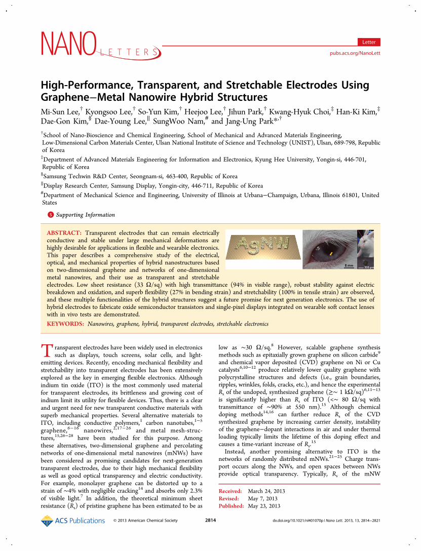
spinning a suspension of Ag nanowires (AgNWs) onto a CVD-synthesized graphene layer, and AgNWs are attached tographene through van der Waals force (see SupportingInformation). Figure 1a presents a photo and SEM image ofthe graphene−AgNW hybrid film on a PET substrate. Asshown in the AFM image of Figure S2a, the average diameterand length of the AgNWs are 20 nm and 30 μm, respectively.The average density of the NWs coated on the graphenesurface is controlled within the range between 640 ± 300 and3730 ± 114 NWs per 100 × 100 μm2 area (Figure 1b) usingdifferent spin rates. Lower spin rates result in smaller deviationsof the NW density and better uniformity (Supporting Table 1),which causes smaller deviations of sheet resistance values(Figure 1d). These densities belong to the percolation regime.For example, conductive paths along solely AgNWs are yieldedwhen the NWs with the similar density range are coated on thePET with no graphene. Figure 1c plots the transmittances forthe graphene−AgNW hybrid films with several different NWdensities. These transmittances are higher than 94% in thevisible range and almost consistent in the broad range from 400to 1500 nm. Unlike the single material of graphene or AgNWs,only ∼2−3% loss of transmittance is introduced by forming thehybrid structure (Figure S2b). This high transparency of the
Figure 1. Fabrication and quantitative analysis of graphene−AgNW hybrid nanostructures. (a) Photograph of graphene−AgNW hybrid film on aPET substrate. The scale bar indicates 2 cm. The inset shows a SEM image of this hybrid (scale bar, 5 μm). (b) Dependence of AgNW density (inthe area of 100 × 100 μm2) on spin rate. (c) Optical transmittance spectra of the hybrid films where AgNWs are coated with different spin rates. (d)Log-scale plots of the sheet resistances as a function of NW density.
Nano Letters Letter
dx.doi.org/10.1021/nl401070p | Nano Lett. 2013, 13, 2814−28212815
hybrid in the visible light is comparable to ITO, and theirtransmittances in the near-infrared region are superior thanITO that has strong absorption for wavelengths over 1100nm.22 As shown in Figure 1d, the Rs of the hybrid film can bereduced with increasing the density of AgNWs via themodulation of the spin rate, and the lowest Rs of 33 Ω/sqwith the transmittance of 94% (at 550 nm) was achieved. ThisRs is significantly lower than that of the CVD graphene (Rs ≥ ∼1 kΩ/sq) and comparable to the ITO electrode.We compared the resistance of this hybrid nanostructure
(Rs,hybrid) to the case where two singular components ofgraphene and AgNWs are connected as resistors in parallelwithout forming the hybrid geometry (Figure S2c). Sheetresistance in this parallel circuit (Rs,parallel) can be calculated,according to 1/Rs,parallel = 1/Rs,graphene + 1/Rs,AgNW. For thiscalculation, Rs,graphene (1.02 kΩ/sq) and Rs,AgNW were exper-imentally measured after producing graphene and AgNWnetworks separately. Figure S2c indicates Rs,hybrid is lower thanRs,parallel overall, which means two components of the grapheneand AgNWs in the hybrid form do not provide independentpathways for carriers but improve their own conductancescomplementarily. For example, the AgNW bridges acrossdefects of the polycrystalline graphene can reduce the resistanceof graphene significantly,29−31 and graphene occupying emptyspaces of the AgNW network also can improve the
conductance. The relative difference in Rs values of the parallelcircuit model and the hybrid electrode can fall below 20%,which indicates that the dense network of AgNWs becomes themain conductive component and graphene acts as an additionalcomponent, as the density of AgNWs increases (Figure S2d).Electrical properties can be changed by pattern geometries.
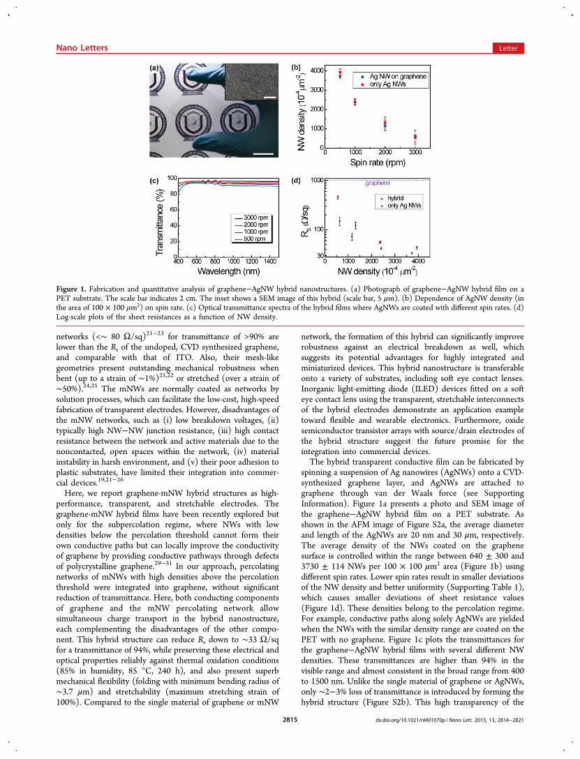
For this study, we photolithographically patterned the threematerials (graphene, AgNWs, and the hybrid) with variouswidths and lengths using oxygen plasma exposure and wetetching (see Supporting Information and Figure 2a), and thenmeasured their resistances to compare the Rs after depositingtwo contact pads of metals (2 nm thick Cr and 300 nm thickAu). As shown in Figure 2b, Rs of the AgNW network shows alarge variation by changing widths of patterns because locallydisconnected areas are produced by etching NWs. In contrastto a 2D graphene layer that presents negligible dependence ofRs on the pattern width, for example, Rs of the AgNW networkincreases significantly as the width decreases to the level similarto the NW length (∼30 μm) and becomes nonconductive forthe width less than 20 μm (at the case of 500 μm in patternlength). In addition, the Rs dependent on the width can vary bychanging the pattern length as well (Figure S4). For example,the narrow widths below 20 μm can be conductive for shortlengths of patterns (length < 100 μm). This Rs dependence onwidth and length can yield undesirable, local changes in
Figure 2. Electrical properties of the hybrid patterns. (a) Optical images of graphene−AgNW hybrid electrodes with different pattern widths. Thescale bar is 200 μm. (b) Dependence of sheet resistance on the width of patterns (pattern length: 500 μm). The Y-axis in the graph is plotted on alogarithmic scale. (c) I−V characteristics of AgNWs, graphene, and their hybrid patterns (pattern width: 10 μm, length: 50 μm). (d) Dependence ofthe breakdown electric fields on the length of patterns (pattern width: 10 μm). The Y-axis in the graph is plotted on a logarithmic scale. (e) Log-scaleplots of the max current versus pattern length for these three materials (pattern width: 10 μm).
Nano Letters Letter
dx.doi.org/10.1021/nl401070p | Nano Lett. 2013, 13, 2814−28212816
resistance of circuits, and hence can limit the use of AgNWs fordesigning compactly integrated circuits that require diverse andfine electrode geometries. On the other hand, the graphene−AgNW hybrid electrode presents negligible dependence of Rs
on pattern structures similar to graphene but preservessignificantly lower Rs even for narrow patterns below 20 μmin width (Figure 2b). These sizes (5−20 μm in width) arecomparable to the dimensions of electrodes for recent displaysand touch-screen panels. This consistency in Rs and highconductance are advantages of the hybrid electrode.In addition, the robustness of conductive materials that can
withstand electrical load becomes one of important features, asdevices are highly integrated and miniaturized. The I−Vcharacteristics of graphene, AgNWs, and the hybrid withvarious lengths (L) of patterns were measured in ambient air.As an example, Figure 2c presents breakdown behaviors of thethree materials for a 50 μm-long and 10 μm-wide pattern. Theslopes in the I−V curves indicate conductances, and the narrowpattern size caused the relatively large resistance (∼2 kΩ) ofAgNW networks, compared to resistance of the hybrid, becauseonly small portions of conductive pathways along the NWsremained inside the patterns. For all of the three, currents
increase almost linearly with the applied bias before theirbreakdowns. Figure 2d compares the breakdown electric fields(Ebreakdown) from various L of these three different materials. Inthe case of AgNW network that can be degraded byelectromigration,32 the breakdown occurs at a relatively lowbias (Ebreakdown < 0.1 V/μm) for L ≥ ∼ 30 μm (average lengthof AgNWs), due to the large aspect ratio of NWs and NW−NW contact resistances. This Ebreakdown increases with reducingL below 30 μm, because more NWs can bridge two metalcontact pads directly without NW−NW junctions. On theother hand, the Ebreakdown of CVD graphene is bigger about 10-fold compared to the AgNW network, as shown in Figure 2d.This polycrystalline graphene can be damaged by Joule heatingand oxidation at the defect sites,33 and the Ebreakdown ofgraphene also increases when L falls below the thresholdrelated to grain sizes. In the graphene−AgNW hybridnanostructure, graphene underneath AgNWs can create apath to dissipate heat and electric stress, which can makeAgNWs sustainable against breakdown at relatively high electricfields. Therefore the hybrid exhibits the highest values ofEbreakdown among the three materials (graphene, AgNWnetworks, and the hybrid). Also, the hybrid electrode can
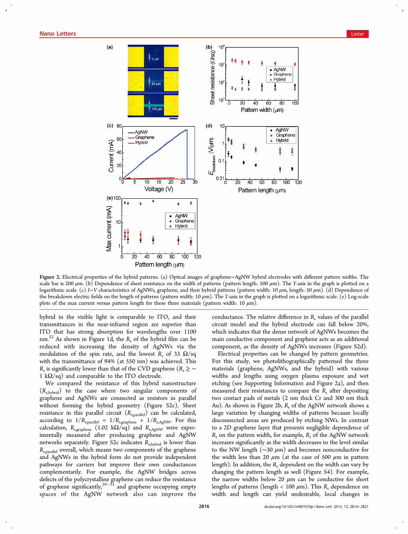
Figure 3. Mechanical properties and reliability of the hybrid nanostructures. (a) Photos of the hybrid electrodes wrapped on various cylindricalsupports with different curvatures. In the middle and right parts of (a), are a photo and SEM image of the hybrid sample folded in half (radius ofcurvature: ∼3.7 μm), respectively. Black scale bar, 5 mm. White scale bar, 50 μm. (b) Relative difference in resistance as a function of radius ofcurvature. (c) A photograph of the hybrid film on a PDMS substrate which is rested on a paper. Scale bar, 5 mm. (d) Relative change in theresistance as a function of tensile strain. (e) Plot of the sheet resistance versus time for graphene, AgNWs, and their hybrid films after exposure tohumid and hot air (temperature: 85 °C, humidity: 85%) for 240 h.
Nano Letters Letter
dx.doi.org/10.1021/nl401070p | Nano Lett. 2013, 13, 2814−28212817
flow the highest current against its breakdown due to its lowresistance, as shown in Figure 2e. This improved robustness ofthe hybrid against electrical load is another advantage.Flexible and stretchable electronics represents an important
application area that can take advantage of the graphene−AgNW hybrid nanostructures. We demonstrate the ultimateflexibility (folding capability) of the hybrid electrode in Figure3. To realize this, a CVD graphene layer was transferred onto a2 μm thick polyimide substrate, followed by spin-coating ofAgNWs (see Supporting Information). As shown in Figure 3a,the hybrid electrodes were wrapped on various cylindricalsupports with different curvatures, and folded in half bypressing two pieces of Si wafer using tape to attach both ends ofthe polyimide to the wafer. The right inset presents a SEMimage of the folded area (radius of curvature: ∼3.7 μm). Figure3b shows the relative difference in Rs as a function of bending-induced strain (ε).6,14 Although this folding leads to a strain of∼27%, no significant change in Rs occurs for the bending toradii of curvature as small as 3.7 μm. In addition, the largeelasticity of graphene34 and the mesh geometry of AgNWnetworks24,25,35 enable the hybrid electrodes to be stretchablemechanically with preserving electric resistance. For themeasurement of the stretchable characteristics of the hybrid,a PDMS elastomeric substrate was used instead of thepolyimide. Figure 3c presents a photograph of the hybrid filmon PDMS which is rested on a paper to demonstrate itstransparent properties. After clamping this conductive sampleby two fixtures connected to the current−voltage measurementsystem, it was stretched to specific elongation lengths using a
mechanical apparatus. Figure 3d shows the relative change inthe resistance under various tensile strains, and the hybridelectrode can be stretched up to 100% tensile strain withnegligible resistance change. This mechanical stability of thehybrid nanostructure against bending and stretching is superiorcompared to ITO that can be cracked by applying a bending ortensile strain of ∼1%.Furthermore, we tested thermal oxidation stabilities of
graphene, AgNWs, and the hybrid. For this test, the hybridfilm was formed by transferring the graphene onto a PET filmwhere AgNWs were precoated, and then exposed to thecondition at 85 °C and 85% RH for 240 h. It has been knownthat AgNWs are oxidized when it is exposed to air.22,23,26 X-raydiffraction (XRD) and energy dispersive spectroscopy (EDS)measurements of the AgNW film clearly confirms the formationof silver oxides after the thermal oxidation stability test (FigureS5). The formation of silver oxide on the surface of AgNWincreases the contact resistance among NWs, which results inincreasing Rs of AgNW networks (Figure 3e). In contrast, thegraphene−AgNW hybrid film exhibits negligible change in Rsbecause oxygen gas and moisture cannot permeate through thegraphene layer consistent with previous literature.36,37 Here thegraphene covering AgNWs can act as a passivation layer toretard Ag oxidation as well as providing conductive paths.As a demonstration of device fabrication using the hybrid
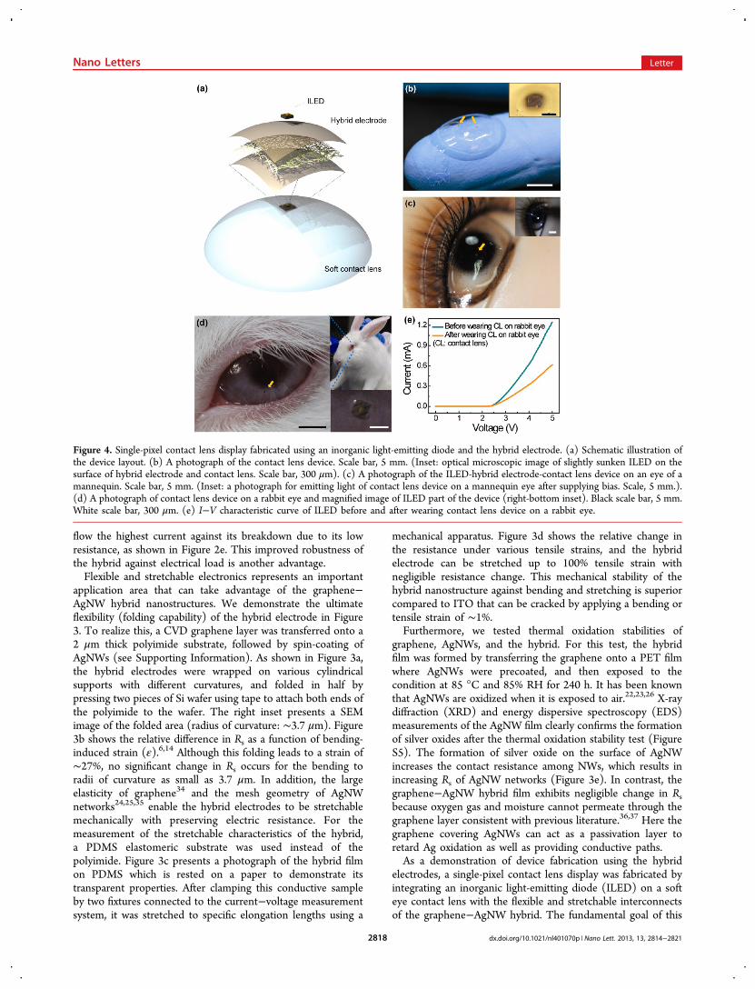
electrodes, a single-pixel contact lens display was fabricated byintegrating an inorganic light-emitting diode (ILED) on a softeye contact lens with the flexible and stretchable interconnectsof the graphene−AgNW hybrid. The fundamental goal of this
Figure 4. Single-pixel contact lens display fabricated using an inorganic light-emitting diode and the hybrid electrode. (a) Schematic illustration ofthe device layout. (b) A photograph of the contact lens device. Scale bar, 5 mm. (Inset: optical microscopic image of slightly sunken ILED on thesurface of hybrid electrode and contact lens. Scale bar, 300 μm). (c) A photograph of the ILED-hybrid electrode-contact lens device on an eye of amannequin. Scale bar, 5 mm. (Inset: a photograph for emitting light of contact lens device on a mannequin eye after supplying bias. Scale, 5 mm.).(d) A photograph of contact lens device on a rabbit eye and magnified image of ILED part of the device (right-bottom inset). Black scale bar, 5 mm.White scale bar, 300 μm. (e) I−V characteristic curve of ILED before and after wearing contact lens device on a rabbit eye.
Nano Letters Letter
dx.doi.org/10.1021/nl401070p | Nano Lett. 2013, 13, 2814−28212818
future display is to create see-through contact lens devices thatcan overlay visual information on the real world, providingimmediate, hands-free access to information.38−40 Here, animportant challenge is the safe operation of this display on alive eye, and hence it is necessary to adapt the devices towearable contact lenses, including hydrogel-type soft lenses,instead of to lens-shaped PET substrates that have poor oxygenpermeability. The transparent and stretchable characteristics ofthe graphene−AgNW hybrid electrodes can provide goodelectrical interfaces between the rigid ILED and deformable,soft contact lens substrate. The fabrication process began withthe CVD synthesis of graphene on a Cu foil. After coatingAgNW networks on the graphene surface, another graphenepassivation layer covered the NWs to prevent the possible lossof the NWs by tears. Patterning the hybrid nanostructure usingoxygen plasma followed by etching the Cu foil and thentransferring the hybrid electrode onto a soft contact lens (softgalyfilcon A polymer). Placing light-emitting diodes (RazerThinRT290, Cree, Inc.) on the top surface of the electrodes using atweezer completed the fabrication step. Figure 4a and b shows aschematic diagram of the device layouts and photographs ofthis sample. The contact lens area under the ILED (dimension:270 μm × 270 μm × 95 μm) becomes sunk down slightly dueto the ILED weight (inset of Figure 4b). The superb flexibilityand stretchability of this hybrid electrode enable its planarlayout to be wrapped on the curved, hemispherical outsidesurface of the contact lens comfortably. Figure 4c presents theILED sample worn on the eye of a mannequin, and this devicecan operate to emit light by supplying bias of 4 V (SupportingMovie 1). As an in vivo study, this contact lens was worn by alive rabbit eye for five hours (Figure 4d), and we have notobserved any abnormal behavior of the live rabbit (Female NewZealand White Rabbit), such as bloodshot eyes or the rubbingof eye areas. Supporting Movie 2 shows the movement of therabbit with wearing the contact lens device. After wearing forfive hours, the contact lens was removed from the ocularsurface to measure the current−voltage characteristics of the
device using a probe station. As shown in Figure 4e, the ILEDon the contact lens is still working with emitting light. Theturn-on voltage is maintained after this in vivo experiment, butresistance is increased (i.e., slope is lowered) due to the slightslipping of ILED on the surface of the hybrid electrode by theregular eye nictation of the live rabbit. The developments ofbiocompatible and conductive adhesives, fabrications ofmultiple pixel displays on wearable contact lenses, andintegrations of antennas for wireless power transmissionrepresent next steps toward the future displays.The graphene−AgNW hybrid electrode can be used as
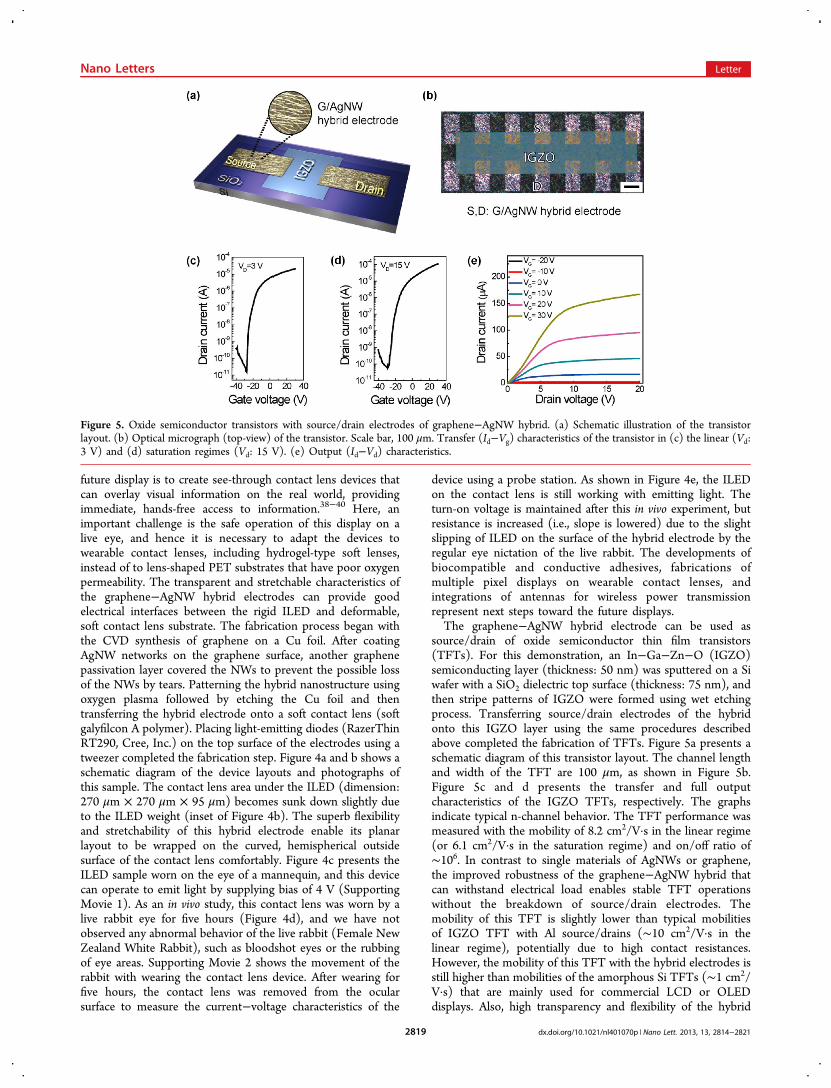
source/drain of oxide semiconductor thin film transistors(TFTs). For this demonstration, an In−Ga−Zn−O (IGZO)semiconducting layer (thickness: 50 nm) was sputtered on a Siwafer with a SiO2 dielectric top surface (thickness: 75 nm), andthen stripe patterns of IGZO were formed using wet etchingprocess. Transferring source/drain electrodes of the hybridonto this IGZO layer using the same procedures describedabove completed the fabrication of TFTs. Figure 5a presents aschematic diagram of this transistor layout. The channel lengthand width of the TFT are 100 μm, as shown in Figure 5b.Figure 5c and d presents the transfer and full outputcharacteristics of the IGZO TFTs, respectively. The graphsindicate typical n-channel behavior. The TFT performance wasmeasured with the mobility of 8.2 cm2/V·s in the linear regime(or 6.1 cm2/V·s in the saturation regime) and on/off ratio of∼106. In contrast to single materials of AgNWs or graphene,the improved robustness of the graphene−AgNW hybrid thatcan withstand electrical load enables stable TFT operationswithout the breakdown of source/drain electrodes. Themobility of this TFT is slightly lower than typical mobilitiesof IGZO TFT with Al source/drains (∼10 cm2/V·s in thelinear regime), potentially due to high contact resistances.However, the mobility of this TFT with the hybrid electrodes isstill higher than mobilities of the amorphous Si TFTs (∼1 cm2/V·s) that are mainly used for commercial LCD or OLEDdisplays. Also, high transparency and flexibility of the hybrid
Figure 5. Oxide semiconductor transistors with source/drain electrodes of graphene−AgNW hybrid. (a) Schematic illustration of the transistorlayout. (b) Optical micrograph (top-view) of the transistor. Scale bar, 100 μm. Transfer (Id−Vg) characteristics of the transistor in (c) the linear (Vd:3 V) and (d) saturation regimes (Vd: 15 V). (e) Output (Id−Vd) characteristics.
Nano Letters Letter
dx.doi.org/10.1021/nl401070p | Nano Lett. 2013, 13, 2814−28212819
electrode are advantageous for transparent and flexible TFTarrays, and this process is currently underway.In conclusion, the work presented here demonstrates the
advantages of graphene−AgNW hybrid nanostructures asflexible and stretchable, transparent electrodes. Integration oftwo-dimensional graphene and one-dimensional NWs in ahybrid film could significantly enhance electrical propertiessuch as low Rs and strong robustness against electricalbreakdown, with negligible degradation of optical trans-mittance. The graphene layer which covers AgNWs reliablypreserves these properties against thermal oxidation. Also, thehybrid electrode presents superb mechanical flexibility andstretchability that enables complete folding in half. Fabricationsof oxide semiconductor transistors and single-pixel displays onwearable, soft eye contact lenses with in vivo studies provideexamples of the use of the hybrid electrodes. We believe thehybridization between two-dimensional and one-dimensionalnanomaterials presents a promising strategy toward flexible,wearable electronics and implantable biosensor devices andindicates the substantial promise of future electronics.
■ ASSOCIATED CONTENT*S Supporting InformationExperimental details of CVD graphene synthesis, AgNWcoating, transfer of the hybrid structures, device fabrications,and supporting figures and movies. This material is availablefree of charge via the Internet at http://pubs.acs.org.
■ AUTHOR INFORMATIONCorresponding Author*E-mail: [email protected].
NotesThe authors declare no competing financial interest.
■ ACKNOWLEDGMENTSThe authors thank Prof. Sung Jun Kang for ILED support. Thiswork was supported by the National Research Foundation ofKorea (20110014111) and the Ministry of KnowledgeEconomy through the Materials Original Technology Program(10041222), IT R&D program (10041416), and New &Renewable Energy Technology Development Program(20113020010060). J.-U.P. thanks UNIST and SamsungDisplay for financial support through the 2012 ResearchFund (1.120001.01).
■ REFERENCES(1) Burroughes, J. H.; Bradley, D. D. C.; Brown, A. R.; Marks, R. N.;Mackay, K.; Friend, R. H.; Burns, P. L.; Holmes, A. B. Light-EmittingDiodes Based on Conjugated Polymers. Nature 1990, 347, 539−541.(2) Yu, G.; Cao, A.; Lieber, C. M. Large-area Blown Bubble Films ofAligned Nanowires and Carbon Nanotubes. Nat. Nanotechnol. 2007, 2,372−377.(3) Park, J.-U.; Meitl, M. A.; Hur, S.-H.; Usrey, M. L.; Strano, M. S.;Kenis, P. J. A.; Rogers, J. A. In-situ Deposition and Patterning ofSingle-Walled Carbon Nanotubes By Laminar Flow and ControlledFlocculation in Microfluidic Channels. Angew. Chem., Int. Ed. 2006, 45,581−585.(4) Wu, Z.; Chen, Z.; Du, X.; Logan, M. J.; Sippel, J.; Nikolou, M.;Karamas, K.; Reynolds, J. R.; Tanner, D. B.; Hebard, A. F.; et al.Transparent, Conductive Carbon Nanotube Films. Science 2004, 305,1273−1276.(5) Shim, B. S.; Zhu, J. A.; Jan, E.; Critchley, K.; Kotov, N. A.Transparent Conductors form Layer-by-Layer Assembled SWNT
Films: Importance of Mechanical Properties and a New Figure ofMerit. ACS Nano 2010, 4, 3725−3734.(6) Park, J.-U.; Nam, S.; Lee, M.-S.; Lieber, C. M. Synthesis ofMonolithic Graphene-Graphite Integrated Electronics. Nat. Mater.2012, 11, 120−125.(7) Nair, R. R.; Blake, P.; Grigorenko, A. N.; Novoselov, K. S.; Booth,T. J.; Stauber, T.; Peres, N. M. R.; Geim, A. K. Fine Structure ConstantDefines Visual Transparency of Graphene. Science 2008, 320, 1308.(8) Chen, J.-H.; Jang, C.; Xiao, S.; Ishigami, M.; Fuhrer, M. S.Intrinsic and Extrinsic Performance Limits of Graphene Devices onSiO2. Nat. Nanotechnol. 2008, 3, 206−209.(9) Emtsev, K. V.; Bostwick, A.; Horn, K.; Jobst, J.; Kellogg, G. L.;Ley, L.; McChesney, J. L.; Ohta, T.; Reshanov, S. A.; Rohrl, J. TowardsWafer-size Graphene Layers by Atmospheric Pressure Graphitizationof Silicon Carbide. Nat. Mater. 2009, 8, 203−207.(10) Reina, A.; Jia, X.; Ho, J.; Nezich, D.; Son, H.; Bulovic, V.;Dresselhaus, M. S.; Kong, J. Large Area, Few-Layer Graphene Films onArbitrary Substrates by Chemical Vapor Deposition. Nano Lett. 2008,9, 30−35.(11) Li, X.; Cai, W.; An, J.; Kim, S.; Nah, J.; Yang, D.; Piner, R.;Velamakanni, A.; Jung, I.; Tutuc, E. Large-Area Synthesis of High-Quality and Uniform Graphene Films on Copper Foils. Science 2009,324, 1312−1314.(12) Kim, K. S.; Zhao, Y.; Jang, H.; Lee, S. Y.; Kim, J. M.; Kim, K. S.;Ahn, J. H.; Kim, P.; Choi, J. Y.; Hong, B. H. Large-Scale PatternGrowth of Graphene Films for Stretchable Transparent Electrodes.Nature 2009, 457, 706−710.(13) Li, X. S.; Zhu, Y. W.; Cai, W. W.; Borysiak, M.; Han, B. Y.;Chen, D.; Piner, R. D.; Colombo, L.; Ruoff, R. S. Nano Lett. 2009, 9,4359−4363.(14) Bae, S.; Kim, H.; Lee, Y.; Xu, X.; Park, J.-S.; Zheng, Y.;Balakrishnan, J.; Lei, T.; Kim, H. R.; Song, Y. I.; Kim, Y.-J.; Kim, K. S.;Ozyilmaz, B.; Ahn, J.-H.; Hong, B. H.; Iijima, S. Roll-to-RollProduction of 30 in. Graphene Films for Transparent Electrodes.Nat. Nanotechnol. 2010, 5, 574−578.(15) Zhu, Y.; Sun, Z.; Yan, Z.; Jin, Z.; Tour, J. M. Rational Design ofHybrid Graphene Films for High-Performance Transparent Electro-des. ACS Nano 2011, 5, 6472−6479.(16) Kim, K. K.; Reina, A.; Shi, Y.; Park, H.; Li, L.-J.; Lee, Y. H.;Kong, J. Enhancing the Conductivity of Transparent Graphene Filmsvia Doping. Nanotechnology 2010, 21, 285205.(17) Lieber, C. M. Semiconductor Nanowires: A Platform forNanoscience and Nanotechnology. MRS Bull. 2011, 36, 1052−1063.(18) Wang, C.; Hu, Y.; Lieber, C. M.; Sun, S. Ultrathin Au Nanowiresand Their Transport Properties. J. Am. Chem. Soc. 2008, 130, 8902−8903.(19) Wu, Y.; Xiang, J.; Yang, C.; Lu, W.; Lieber, C. M. Single-crystalMetallic Nanowires and Metal/semiconductor Nanowire Hetero-structures. Nature 2004, 430, 61−65.(20) Wang, D.; Lieber, C. M. Inorganic Materials; NanocrystalsBranch Out. Nat. Mater. 2003, 2, 355−356.(21) De, S.; Higgins, T. M.; Lyons, P. E.; Doherty, E. M.; Nirmalraj,P. N.; Blau, W. J.; Boland, J. J.; Coleman, J. N. Silver NanowireNetworks as Flexible, Transparent, Conducting Films: Extremely HighDC to Optical Conductive Ratios. ACS Nano 2009, 3, 1767−1774.(22) Hu, L.; Kim, H. S.; Lee, J.-Y.; Peumans, P.; Cui, Y. ScalableCoating and Properties of Transparent, Flexible, Silver NanowireElectrodes. ACS Nano 2010, 4, 2955−2963.(23) De, S.; Coleman, J. N. The Effects of Percolation inNanostructured Transparent Conductors. MRS Bull. 2011, 36, 774−781.(24) Yang, L.; Zhang, T.; Zhou, H.; Price, S. C.; Wiley, B. J.; You, W.Solution-Processed Flexible Polymer Solar Cells with Silver NanowireElectrodes. ACS Appl. Mater. Interfaces 2011, 3, 4075−4084.(25) Hu, W.; Niu, X.; Li, L.; Yun, S.; Yu, Z.; Pei, Q. IntrinsicallyStretchable Transparent Electrodes Based on Silver-Nanowire-Cross-linked-Polyacrylate Composites. Nanotechnology 2012, 23, 344002.(26) Hu, L.; Wu, H.; Cui, Y. Metal Nanogrids, Nanowires, andNanofibers for Transparent Electrodes. MRS Bull. 2011, 36, 760−765.
Nano Letters Letter
dx.doi.org/10.1021/nl401070p | Nano Lett. 2013, 13, 2814−28212820

(27) Catrysse, P. B.; Fan, S. H. Nanopatterned Metallic Films for UseAs Transparent Conductive Electrodes in Optoelectronic Devices.Nano Lett. 2010, 10, 2944−2949.(28) Ahn, S. H.; Guo, L. J. Spontaneous Formation of PeriodicNanostructures by Localized Dynamic Wrinkling. Nano Lett. 2010, 10,4228−4234.(29) Jeong, C.; Nair, P.; Khan, M.; Lundstrom, M.; Alam, M. A.Prospects for Nanowire-Doped Polycrystalline Graphene Films forUltratransparent, High Conductive Electrodes. Nano Lett. 2011, 11,5020−5025.(30) Kholmanov, I. N.; Stoller, M. D.; Edgeworth, J.; Lee, W. H.; Li,H.; Lee, J.; Barnhart, C.; Potts, J. R.; Piner, R.; Akinwande, D.; Barrick,J. E.; Ruoff, R. S. Nanostructured Hybrid Transparent ConductiveFilms with Antibacterial Properties. ACS Nano 2012, 6, 5157−5163.(31) Kholmanov, I. N.; Magnuson, C. W.; Aliev, A. E.; Li, H.; Zhang,B.; Suk, J. W.; Zhang, L. L.; Peng, E.; Mousavi, S. H.; Khanikaev, A. B.;Piner, R.; Shvets, G.; Ruoff, R. S. Improved Electrical Conductivity ofGraphene Films Integrated with Metal Nanowires. Nano Lett. 2012,12, 5679−5683.(32) Zhao, J.; Sun, H.; Dai, S.; Wang, Y.; Zhu, J. Electrical Breakdownof Nanowires. Nano Lett. 2011, 11, 4647−4651.(33) Kang, C. G.; Lee, S. K.; Lee, Y. G.; Hwang, H. J.; Cho, C.; Lim,S. K.; Heo, J.; Chung, H.-J.; Yang, H.; Seo, S.; Lee, B. H. EnhancedCurrent Drivability of CVD graphene Interconnect in Oxygen-Deficient Environment. IEEE Electron Device Lett. 2011, 32, 1591−1593.(34) Lee, C.; Wei, X.; Kysar, J. W.; Hone, J. Measurement of theElastic Properties and Intrinsic Strength of Monolayer Graphene.Science 2008, 321, 385−388.(35) Kim, D.-H.; Rogers, J. A. Stretchable Electronics: MaterialsStrategies and Devices. Adv. Mater. 2008, 20, 4887−4892.(36) Bunch, S.; Verbridge, S. S.; Alden, J. S.; van der Zande, A. M.;Parpia, J. M.; Craighead, H. G.; McEuen, P. L. Impermeable AtomicMembranes from Graphene Sheets. Nano Lett. 2008, 8, 2458−2462.(37) Chen, S.; Brown, L.; Levendorf, M.; Cai, W.; Ju, S.; Edgeworth,J.; Li, X.; Magnuson, C. W.; Velamakanni, A.; Piner, R. D.; Kang, J.;Park, J.; Ruoff, R. S. Oxidation Resistance of Graphene-Coated Cu andCu/Ni Alloy. ACS Nano 2011, 5, 1321−1327.(38) Lingley, A. R.; Ali, M.; Liao, Y.; Mirjalili, R.; Klonner, M.;Sopanen, M.; Suihkonen, S.; Shen, T.; Otis, B. P.; Lipsanen, H.; Parviz,B. A. A Single-Pixel Wireless Contact Lens Display. J. Micromech.Microeng. 2011, 21, 125014.(39) Stauth, S. A.; Parviz, B. A. Self-Assembled Single-crystal SiliconCircuits on Plastic. Proc. Natl Acad. Sci. 2006, 103, 13922−7.(40) Parviz, B. A. For Your Eye Only. IEEE Spectrum 2009, 46, 36−41.
Nano Letters Letter
dx.doi.org/10.1021/nl401070p | Nano Lett. 2013, 13, 2814−28212821