high-speed analog-to-digital converters in cmos
TRANSCRIPT
SIYU
TAN
H
igh-Speed Analog-to-D
igital Converters in C
MO
S 2020
Lund UniversityFaculty of Engineering
Department of Electrical and Information Technology
978-91-7895-688-3 (print)978-91-7895-689-0 (pdf)ISSN 1654-790X No. 134
High-Speed Analog-to-Digital Converters in CMOSSIYU TAN
DEP. OF ELECTRICAL AND INFORMATION TECHNOLOGY | LTH | LUND UNIVERSITY
9789178
956883


High-Speed Analog-to-Digital
Converters in CMOS
by Siyu Tan
Doctoral Dissertation
Supervisors: Associate Prof. Pietro Andreani, Prof. Henrik SjolandFaculty opponent: Prof. Piero Malcovati
To be presented, with the permission of the Faculty of Engineering, LTH at Lund Univer-
sity, for public criticism in lecture hall E:C at the Department of Electrical and Information
Technology, Ole Romers vag 3, 223 63 Lund, Sweden, on Friday, the 18th of December 2020
at 09:00 a.m.

A doctoral thesis at a university in Sweden takes either the form of a single,cohesive research study (monograph) or a summary of research papers (compil-ation thesis), which the doctoral student has written alone or together with oneor several other author(s).
In the latter case the thesis consists of two parts. An introductory text putsthe research work into context and summarizes the main points of the papers.Then, the research publications themselves are reproduced, together with adescription of the individual contributions of the authors. The research papersmay either have been already published or are manuscripts at various stages (inpress, submitted, or in draft).
Cover illustration front: an ADC CMOS chip layout and its circuit board photo, tobe integrated into high-performance communication devices in the future.
Cover illustration back: a prototype ADC CMOS chip bonded on a circuit board.
� Siyu Tan 2020
Faculty of Engineering, LTH, Department of Electrical and Information Technology
isbn: 978-91-7895-688-3 (print)isbn: 978-91-7895-689-0 (pdf)issn: 1654-790X; No. 134
Printed in Sweden by Media-Tryck, Lund University, Lund 2020

Popular Summary
Technology advancements in the 21st century create a vast amount of possibilit-ies, allowing us to make strides that our ancestors could only dream of. Commu-nication systems improved greatly in the past several decades. The developmentof these systems closely follows the evolution of cellular mobile network stand-ards to the latest commercialized 5G: the fifth generation that starts deployingglobally. The emerging 5G communication systems enable reliable connectionswith significantly reduced latency at an increased transmission rate. Commu-nication among people is not limited to voice-only anymore but extended tomore versatile formats such as video chat and multimedia message. It is alreadyan essential part of our daily lives: communication among us is through smartdevices besides face-to-face.
Nowadays, the rapid development of high-performance handheld devices facilit-ates fast and secure access to the Internet: a global system that connects peopleworldwide. We share lives, acquire new knowledge, learn history, and explorethe world without leaving home by merely surfing the Internet. The ever in-creased demands of smooth surfing experiences increase current communicationsystems’ pressure and bring up the stringent requirements for technology ad-vancement of next-generation communication devices. They prefer low latency,stable and fast upload/download transmission speed, and broad coverage withlow energy dissipation.
The advance of communication systems will not be successful without the high-performance Analog to Digital Converter (ADC), an essential component in amodern high-performance radio transceiver device. The ADC acts as a bridgeconnecting the analog and the digital domain. Usually, the analog domainsignals are real-world analog measurable physical quantities, such as voltage orcurrent. However, the high-performance processors are entirely digital and onlycapable of processing signals in the digital format.
High-performance ADCs are capable of immediately digitalizing the analog sig-
iii

nal at high-speed. A high-speed ADC coping with a high-speed digital processorcan digitalize the input analog signals. It allows very flexible, reliable, and highlypower-efficient digital signal processing, filtering and calibrating the digital sig-nal in real-time. All the great features are possible thanks to the maturityof Complementary Metal Oxide Semiconductor (CMOS) technology nodes inintegrated circuits.
The main focus of this research is designing high-performance ADCs on in-tegrated circuits. This research analyzes various ADC architectures and theircomponent-level implementations in advanced CMOS technologies. This re-search aims to find optimized designs for high-speed analog-to-digital conver-sion, understand their benefits and limitations, and evaluate the possibilities ofintegrating them inside the advanced base station devices in the future.
The author performed extensive literature studies to examine the state-of-the-art designs from the research field and industry before the actual circuit designs.The ADC specifications and requirements are carefully drawn up. This disserta-tion explains the experimented ADC designs in detail and includes the relevantresearch papers at the end.
iv

Abstract
The Analog to Digital (A/D) Converters (ADC) are vital components in high-performance radio devices. In the receiver end, the signal received by the ana-log front-end can not be directly analyzed by the digital core, thus requiringhigh-performance ADC circuits acting as bridges connecting the analog anddigital domain. These circuits are integrated into Complementary Metal-Oxide-Semiconductor (CMOS) chips, which achieve high performance and consumelow power at the same time.
In this research, various types of ADCs are analyzed both in architectural designsand component-level implementations. The goal is to find out optimized circuitdesigns to be used in high-speed communication devices in the future.
Two Successive-Approximation-Register (SAR) ADCs are studied. One of theSAR ADCs is a previously designed synchronous SAR ADC CMOS chip, im-plemented in the 22 nm Fully Depleted Silicon On Insulator (FD-SOI) CMOS,whose measurement results are shown. An estimation and calibration techniquefor linearizing its Digital to Analog Converter (DAC) imbalance is presented.Another SAR ADC is improved from the synchronous version, which has asyn-chronously clocked internal components, designed and implemented in 22 nmFD-SOI.
Two Continuous-Time (CT) ΔΣ ADCs were designed and analyzed. One of theΔΣ ADCs is a high-speed converter implemented in 28 nm FD-SOI CMOS, run-ning at 5GHz sampling frequency and targeting at 250MHz signal bandwidth.Another ΔΣ ADC is implemented in 65 nm CMOS and fabricated. It evalu-ates the effectiveness of digital calibration techniques in linearizing a criticalouter-most DAC in the feedback.
All the ADC designs showing in this work are closely related to the state-of-the-art research works. The design specifications from the industry field are
v

also carefully considered during the design phase. The introductions and thedesign details are explained in the first part of this dissertation, and the relevantresearch papers are attached in the second part.
vi

Contents
Popular Summary iii
Abstract v
List of Publications xi
Acknowledgments xiii
List of Acronyms xv
List of Figures xix
List of Tables xxiii
1 Introduction 11.1 Overview of Radio Communication . . . . . . . . . . . . . . . . . 11.2 Analog to Digital Data Conversion . . . . . . . . . . . . . . . . . 4
1.2.1 Analog to Digital Data Conversion Principle . . . . . . . 41.3 ADC Specifications . . . . . . . . . . . . . . . . . . . . . . . . . . 5
1.3.1 ADC Input Bandwidth . . . . . . . . . . . . . . . . . . . 61.3.2 ADC Resolution . . . . . . . . . . . . . . . . . . . . . . . 71.3.3 ADC Power Consumption . . . . . . . . . . . . . . . . . . 71.3.4 ADC Noise . . . . . . . . . . . . . . . . . . . . . . . . . . 8
1.4 Overview of Nyquist-Rate ADCs . . . . . . . . . . . . . . . . . . 91.5 Overview of Oversampled ADCs . . . . . . . . . . . . . . . . . . 121.6 Relate to State-of-the-Art ADC Designs . . . . . . . . . . . . . . 131.7 Summaries of Experimented ADCs . . . . . . . . . . . . . . . . . 15
2 SAR ADC 172.1 Introduction . . . . . . . . . . . . . . . . . . . . . . . . . . . . . . 172.2 SAR ADC Architecture . . . . . . . . . . . . . . . . . . . . . . . 192.3 TI SAR ADC Architecture . . . . . . . . . . . . . . . . . . . . . 212.4 SAR ADC Clocking Schemes . . . . . . . . . . . . . . . . . . . . 22
2.4.1 Synchronous SAR ADC Clocking Scheme . . . . . . . . . 222.4.2 Asynchronous SAR ADC Clocking Scheme . . . . . . . . 242.4.3 SSAR and ASAR ADC Timing Differences . . . . . . . . 26
vii

2.5 Component-Level Implementations . . . . . . . . . . . . . . . . . 272.5.1 CDAC Design . . . . . . . . . . . . . . . . . . . . . . . . . 282.5.2 Estimation and Calibration of CDAC Imbalance . . . . . 322.5.3 Comparator Design . . . . . . . . . . . . . . . . . . . . . . 332.5.4 SAR Contol Logic Design . . . . . . . . . . . . . . . . . . 39
2.6 SAR ADC Non-Idealities . . . . . . . . . . . . . . . . . . . . . . 422.6.1 Bit Conversion Errors in SSAR ADC . . . . . . . . . . . . 422.6.2 SNDR Degradation at Increased Sampling Rate . . . . . . 462.6.3 Internal Clock Pulse Width Variations in ASAR ADC . . 472.6.4 Extra Capacitance Tuning . . . . . . . . . . . . . . . . . . 482.6.5 Redundancy Technique in SAR ADCs . . . . . . . . . . . 48
3 SSAR and ASAR ADC Chip Photos, Layouts, Simulation andMeasurement Results 533.1 SSAR and ASAR ADC Chip-Level Implementations . . . . . . . 533.2 SSAR ADC Measurement Procedures and Results . . . . . . . . 553.3 SSAR ADC Power Consumption . . . . . . . . . . . . . . . . . . 573.4 ASAR ADC Simulation Results . . . . . . . . . . . . . . . . . . . 593.5 ASAR ADC Power Consumption . . . . . . . . . . . . . . . . . . 613.6 Conclusion . . . . . . . . . . . . . . . . . . . . . . . . . . . . . . 62
4 High-Speed ΔΣ ADC 634.1 Introduction . . . . . . . . . . . . . . . . . . . . . . . . . . . . . . 634.2 Model Construction in MATLAB . . . . . . . . . . . . . . . . . . 65
4.2.1 ΔΣ ADC Model . . . . . . . . . . . . . . . . . . . . . . . 654.2.2 DT Coefficients . . . . . . . . . . . . . . . . . . . . . . . . 67
4.3 DT to CT Transformation . . . . . . . . . . . . . . . . . . . . . . 684.3.1 Impulse-Invariant Transformation . . . . . . . . . . . . . . 684.3.2 DAC Output Pulse Shape . . . . . . . . . . . . . . . . . . 694.3.3 ELD Compensation . . . . . . . . . . . . . . . . . . . . . 694.3.4 Dynamic Range Scaling . . . . . . . . . . . . . . . . . . . 71
4.4 Component-Level Implementation . . . . . . . . . . . . . . . . . 714.4.1 LF Design . . . . . . . . . . . . . . . . . . . . . . . . . . . 724.4.2 Active Summation . . . . . . . . . . . . . . . . . . . . . . 744.4.3 Quantizer Design . . . . . . . . . . . . . . . . . . . . . . . 754.4.4 Current-Steering Feedback DACs . . . . . . . . . . . . . . 754.4.5 CML in Quantizer and DAC . . . . . . . . . . . . . . . . 77
4.5 DAC Unit Cell Mismatches and Tuning . . . . . . . . . . . . . . 784.5.1 Bias Voltage and Current Tuning . . . . . . . . . . . . . . 784.5.2 Digital Tuning . . . . . . . . . . . . . . . . . . . . . . . . 79
4.6 Layout, Simulation, and Measurement Results . . . . . . . . . . . 794.7 Conclusion . . . . . . . . . . . . . . . . . . . . . . . . . . . . . . 83
viii

5 ΔΣ ADC with Digital Background Calibration 855.1 Introduction . . . . . . . . . . . . . . . . . . . . . . . . . . . . . . 855.2 ΔΣ ADC Architecture . . . . . . . . . . . . . . . . . . . . . . . . 865.3 Digital Calibration Algorithm . . . . . . . . . . . . . . . . . . . . 875.4 Component-Level Implementation . . . . . . . . . . . . . . . . . 89
5.4.1 DAC Unit Cell Design . . . . . . . . . . . . . . . . . . . . 895.4.2 Switch Logic Design . . . . . . . . . . . . . . . . . . . . . 905.4.3 Quantizer Design . . . . . . . . . . . . . . . . . . . . . . . 925.4.4 Amplifier Design . . . . . . . . . . . . . . . . . . . . . . . 93
5.5 Simulation and Measurement Results . . . . . . . . . . . . . . . . 945.6 Conclusion . . . . . . . . . . . . . . . . . . . . . . . . . . . . . . 98
6 Summary of Included Papers and Author Contributions 99Paper I:
Digital Background Calibration in Continuous-time ΔΣ Analogto Digital Converters . . . . . . . . . . . . . . . . . . . . . . . . . 99Summary . . . . . . . . . . . . . . . . . . . . . . . . . . . . . . . 99Author Contributions . . . . . . . . . . . . . . . . . . . . . . . . 100
Paper II:A continuous-time delta-sigma ADC with integrated digital back-ground calibration . . . . . . . . . . . . . . . . . . . . . . . . . . 100Summary . . . . . . . . . . . . . . . . . . . . . . . . . . . . . . . 100Author Contributions . . . . . . . . . . . . . . . . . . . . . . . . 100
Paper III:A 5 GHz CT ΔΣ ADC with 250MHz Signal Bandwidth in 28nm-FDSOI CMOS . . . . . . . . . . . . . . . . . . . . . . . . . . 101Summary . . . . . . . . . . . . . . . . . . . . . . . . . . . . . . . 101Author Contributions . . . . . . . . . . . . . . . . . . . . . . . . 101
Paper IV:A 10-bit Split-Capacitor SAR ADC with DAC Imbalance Estim-ation and Calibration . . . . . . . . . . . . . . . . . . . . . . . . 102Summary . . . . . . . . . . . . . . . . . . . . . . . . . . . . . . . 102Author Contributions . . . . . . . . . . . . . . . . . . . . . . . . 102
Paper V:Asynchronous vs. Synchronous CMOS SAR ADCs - A Comparison103Summary . . . . . . . . . . . . . . . . . . . . . . . . . . . . . . . 103Author Contributions . . . . . . . . . . . . . . . . . . . . . . . . 103
Paper VI:A Design Method to Minimize the Impact of Bit Conversion Er-rors in SAR ADCs . . . . . . . . . . . . . . . . . . . . . . . . . . 104Summary . . . . . . . . . . . . . . . . . . . . . . . . . . . . . . . 104
ix

Author Contributions . . . . . . . . . . . . . . . . . . . . . . . . 104
7 Conclusion and Future Work 105
A Coefficient Calculations in DT to CT DSM Architecture Trans-formation with 4th Order CRFF LF 109A.1 The DT DSM Open-Loop Transfer Function . . . . . . . . . . . . 110A.2 DT to CT DSM Transformation . . . . . . . . . . . . . . . . . . 111
A.2.1 DT to CT Transformation - ELD Less than or Equal toOne Clock Period . . . . . . . . . . . . . . . . . . . . . . . 112
A.2.2 DT to CT Transformation - ELD Larger than One ClockPeriod . . . . . . . . . . . . . . . . . . . . . . . . . . . . . 116
References 119
Paper I: Digital Background Calibration in Continuous-time ΔΣAnalog to Digital Converters 127
Paper II: A continuous-time delta-sigma ADC with integrateddigital background calibration 133
Paper III: A 5 GHz CT ΔΣ ADC with 250MHz Signal Band-width in 28 nm-FDSOI CMOS 145
Paper IV: A 10-bit Split-Capacitor SAR ADC with DAC Imbal-ance Estimation and Calibration 151
Paper V: Asynchronous vs. Synchronous CMOS SAR ADCs -A Comparison 159
Paper VI: A Design Method to Minimize the Impact of Bit Con-version Errors in SAR ADCs 169
x

List of Publications
This dissertation is based on the following publications, referred to by theirRoman numerals:
I Digital Background Calibration in Continuous-time ΔΣ Analogto Digital ConvertersSiyu Tan, Yun Miao, Mattias Palm, Joachim Rodrigues and Pietro Andreani
2015 IEEE Nordic Circuits and Systems Conference (NORCAS): NOR-CHIP and International Symposium of System-on-Chip (SoC)
II A continuous-time delta-sigma ADC with integrated digitalbackground calibrationSiyu Tan, Yun Miao, Mattias Palm, Joachim Neves Rodrigues and Pietro Andreani
Analog Integrated Circuits and Signal Processing volume 89, pages273–282 (2016)
III A 5 GHz CT ΔΣ ADC with 250MHz Signal Bandwidth in 28nm-FDSOI CMOSSiyu Tan, Lars Sundstrom, Mattias Palm, Sven Mattisson and Pietro Andreani
2019 IEEE Nordic Circuits and Systems Conference (NORCAS): NOR-CHIP and International Symposium of System-on-Chip (SoC)
IV A 10-bit Split-Capacitor SAR ADC with DAC Imbalance Es-timation and CalibrationSiyu Tan, Daniele Mastantuono, Roland Strandberg, Lars Sundstrom, Pietro An-dreani and Mattias Palm
2020 IEEE International Symposium on Circuits and Systems (ISCAS2020)
xi

V Asynchronous vs. Synchronous CMOS SAR ADCs - A Com-parisonSiyu Tan, Mattias Palm, Daniele Mastantuono, Roland Strandberg, Lars Sundstromand Pietro Andreani
Submitted to: IEEE Access
VI A Design Method to Minimize the Impact of Bit ConversionErrors in SAR ADCsSiyu Tan, Mattias Palm, Daniele Mastantuono, Roland Strandberg, Lars Sundstrom,Sven Mattisson and Pietro Andreani
2020 IEEE Nordic Circuits and Systems Conference (NORCAS): NOR-CHIP and International Symposium of System-on-Chip (SoC)
All papers are reproduced with permission of their respective publishers.
xii

Acknowledgments
It has been an honor for me to pursue my Ph.D. study in the Departmentof Electrical and Information Technology (EIT) in LTH, at Lund University,Sweden. I was given a chance to access the well-equipped research labs in EIT,and acquired a fortune of knowledge and improved my professional skills. Duringmy studies at Lund University, I enjoyed the research environment and wasgiven support from my supervisors, my colleagues, my parents, my girlfriend,my friends, and many other helpful people.
I would especially like to thank my principal supervisor: Associate ProfessorPietro Andreani, and assistant supervisor: Professor Henrik Sjoland. They gaveme priceless guidance throughout my journey of pursuing knowledge. I gotvarious inspirations from you during the paper revisions, technical and non-technical discussions, circuit designs, and measurements. I am grateful for yourpatience and support, providing me with your experience in both academia andindustry.
I want to thank my dear colleagues. Thank you, all the former and currentPh.D. students. I enjoyed the time when we had group meetings and discussions,and I was given many useful suggestions from you when I felt confused aboutboth work and daily life. The administrative staffs at Lund University are verysupportive, who guided me through non-technical matters.
I would also like to thank Ericsson AB, Lund, Sweden, which provided an internopportunity for me to measure my chip and work with the experts in the EricssonResearch department. During that period, I experienced the difference betweenthe academic realm and the industrial world. I would especially like to thank theresearchers in Ericsson Research. Thank you, Mattias Palm, for providing mea significant amount of useful tips and supervising me when I was a Master’sstudent and then during my Ph.D. study. You are very supportive when Iface challenges in projects. Thank you, Lars Sundstrom. You enlightened mewith very constructive comments based on your broad knowledge and inspiring
xiii

ideas during our regular ADC meetings. Thank you, Sven Mattisson. Youare a real expert in analog-system design who taught me so much in manypractical aspects of circuit design! Also, thank you, Martin Anderson, RolandStrandberg, Daniele Mastantuono. Your generous assistance helped me a lotboth in the SSAR ADC measurement and in the ASAR ADC project.
Lastly and importantly, I would like to thank my family: my parents Haihuaand Jiawei, my grandparents, and all my family members. You raised me andsupported me full-heartedly in every way. Thank you, Yuewen. You are mycousin and also my best friend since childhood. Thank you, Qianying, in frontof whom I can always be my true self. Your love and caress save me every timeI am down.
Thank you all, my dear friends. Your encouragements during my study and inmy life are precious. I enjoy the time with you, and the experiences in my Ph.D.study will be an unforgettable memory in my whole life!
xiv
List of Acronyms
AAF Anti-Aliasing Filter
ACL Asynchronous Control Logic
ADC Analog to Digital Converter
ASAR Asynchronous SAR
BS Base Station
CDAC Capacitive Digital to Analog Converter
CIFB Cascade of Integrators with Distributed Feedback
CIFF Cascade of Integrators with Feed-Forward Summation
CMFB Common-Mode Feedback
CML Current Mode Logic
CMOS Complementary Metal-Oxide-Semiconductor
CT Continuous-Time
CRFB Cascade of Resonators with Feedback
CRFF Cascade of Resonators with Feed-Forward Summation
DAC Digital to Analog Converter
DC Direct Current
DFF D-Flip-Flop
DT Discrete-Time
xv

DSM ΔΣ Modulator
DSP Digital Signal Processor
DUT Design Under Test
ELD Excess Loop Delay
ENOB Effective Number of Bits
ETF Error Transfer Function
FD-SOI Fully Depleted Silicon On Insulator
FinFET Fin Field-Effect Transistor
FOMs Schreier Figure of Merit
FOMw Walden Figure of Merit
FPGA Field-Programmable Gate Array
GBW Gain-Bandwidth Product
GSM Global System for Mobile Communications
IC Integrated Circuit
IoT Internet of Things
LDO Low-Dropout Regulator
LF Loop Filter
LPF Low-Pass Filter
LSB Least Significant Bit
LTE Long Term Evolution
LTI Linear Time-Invariant
MIMO Multiple-Input Multiple-Output
MCS Merged Capacitor Switching
NMOS N-Channel Metal-Oxide-Semiconductor
MOM Metal-Oxide-Metal
xvi
MSB Most Significant Bit
NTF Noise Transfer Function
NRZ Non-Return-to-Zero
OBG Out-of-Band Gain
OFDM Orthogonal Frequency-Division Multiplexing
OSR Oversampling Ratio
PCB Printed Circuit Board
PGA Programmable-Gain Amplifier
PMOS P-Channel Metal-Oxide-Semiconductor
PRBS Pseudo-Random Bit Sequence
PVT Process-Voltage-Temperature
RAM Random Access Memory
RF Radio Frequency
RA Residue Amplifier
ROM Read-Only Memory
RZ Return-to-Zero
SA Successive Approximation
SAR Successive Approximation Register
SCL Synchronous Control Logic
SNDR Signal to Noise and Distortion Ratio
SL Switch Logic
S/H Sample and Hold
SFDR Spurious-Free Dynamic Range
SNR Signal to Noise Ratio
SPI Serial Peripheral Interface
xvii

SQNR Signal to Quantization Noise Ratio
SSAR Synchronous SAR
STF Signal Transfer Function
TI Time-Interleaved
TTF Test Transfer Function
xviii

List of Figures
1.1 Conceptual illustration of 5G radio scenario. . . . . . . . . . . . . 31.2 System-level block diagram of a single receiver core in 5G base
station. . . . . . . . . . . . . . . . . . . . . . . . . . . . . . . . . 31.3 An analog to digital conversion example. . . . . . . . . . . . . . 51.4 Graphical illustration of the input signal bandwidth versus the
ADC sampling frequency in the frequency domain, of (a) Nyquist-rate ADC and (b) oversampled ADC. . . . . . . . . . . . . . . . 7
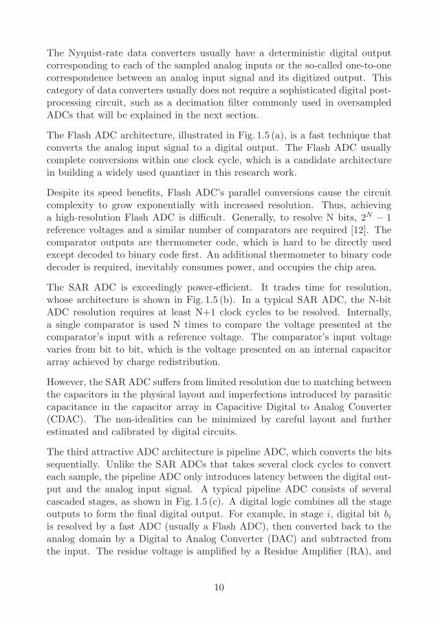
1.5 The Nyquist-rate ADC architectures, including (a) Flash ADC,(b) SAR ADC, and (c) Pipeline ADC. . . . . . . . . . . . . . . . 11
1.6 The ΔΣ ADC architecture. . . . . . . . . . . . . . . . . . . . . . 121.7 A examplar simulated ADC output spectrum with 250MHz signal
bandwidth and sampled at 5GHz. . . . . . . . . . . . . . . . . . 13
2.1 A 6-bit SAR ADC conversion example, with the timing diagramillustration of the ADC input and output signals. . . . . . . . . . 19
2.2 Time-Interleaved ADC architecture, with sampling signals timingdiagram shown at the lower-left corner. . . . . . . . . . . . . . . 21
2.3 N-bit SSAR ADC architecture and critical nodes timing diagram. 232.4 N-bit ASAR ADC architecture and critical nodes timing diagram. 252.5 The timing diagram of (a) an SSAR ADC and (b) an ASAR ADC. 262.6 Component-level implementation of (a) m-bit SSAR ADC and
(b) m-bit ASAR ADC, with one of the CDAC explicitly drawn. 282.7 The CDAC architecture of (a) a bottom plate sampling binary-
weighted CDAC and its controlling switches, and (b) a split ca-pacitor array with a bridge capacitor Cb between the mDAC andthe sDAC. . . . . . . . . . . . . . . . . . . . . . . . . . . . . . . . 29
2.8 10-bit capacitor array with PRBS calibration bits and redund-ancy bit, where (a) shows a complete capacitor array, (b) showsa simplified capacitor array, and (c) shows the actual implement-ation in the presented work. . . . . . . . . . . . . . . . . . . . . 31
2.9 The relationship between Ce and Cb in different BS in the pro-posed 10-bit capacitor array, normalized to Cu. . . . . . . . . . 32
xix

2.10 Theoretical r values, estimated value by the correlation-basedestimator, and estimated value by SNDR maximization sweep,as a function of C ′
e. Capacitor values are normalized to Cu. . . . 332.11 Comparator schematic with either an SR latch or two buffers in
its output stage. . . . . . . . . . . . . . . . . . . . . . . . . . . . 342.12 Pre-amplifier schematic, used in the comparator. . . . . . . . . . 352.13 Regenerative latch timing diagram for a 100mV and a 100 uV
differential latch input voltage Vin. . . . . . . . . . . . . . . . . 362.14 τ vs. input voltage Vin, in a component-level comparator and an
ideal comparator model. . . . . . . . . . . . . . . . . . . . . . . 362.15 τ in ten individual ADC bit conversions, when the ADC input is
a full-scale amplitude sinusoidal signal. . . . . . . . . . . . . . . 372.16 Total conversion time distribution, with input amplitudes of 0 dBFS,
-10 dBFS and -20 dBFS. . . . . . . . . . . . . . . . . . . . . . . . 382.17 A limiter to force a decision within a preset time, digitally tuned
by an adjustable capacitance C, with (a) schematic and (b) timingdiagram. . . . . . . . . . . . . . . . . . . . . . . . . . . . . . . . . 39
2.18 N-bit SCL state machine, including a sampling state Ssmp andbit conversion states SN to S1. . . . . . . . . . . . . . . . . . . . 40
2.19 The SCL schematic, including a ring counter to generate samplingsignal and a control & data generator to generate control signals. 41
2.20 The ACL schematic, including a control & data generator forcontrol signals generation and a clock generator for comparatorclock cmp clk generation. . . . . . . . . . . . . . . . . . . . . . . 41
2.21 Comparator differential outputs vs. clk, when (a) an SR latch isused, and (b) two buffers are used in the comparator output stage. 43
2.22 Conceptual illustration of SCL decision errors when latching com-parator differential outputs, where (a) shows an SCL design withparallel signal paths, and (b) shows a modified SCL design byprocessing single-ended comparator output for generating non-overlapping control signals. . . . . . . . . . . . . . . . . . . . . . 44
2.23 Graphical illustration of Vin after each bit conversion in a 6-bitSAR ADC example. (a) |VMW | is very small, Vin approaches 0reference. (b) The tconv is insufficient, causing a relatively large|VMW |, Vin converges to a new reference voltage −VMW using theproposed method, where the default control signals are d(i) = 1and d(i) = 0. . . . . . . . . . . . . . . . . . . . . . . . . . . . . . 45
2.24 Simulated ADC output spectra, with an ideal error-free resultshown in black; with large |VMW | and buffers in the comparator,shown in blue; with the SR latch in the comparator, shown in red. 45
2.25 SNDR vs. tconv plots, using proposed and standard design. . . . 46
xx

2.26 SNDR vs. sampling frequency sweep. . . . . . . . . . . . . . . . 472.27 A 5-bit binary searching algorithm shows the internal voltage Vi
changes in each bit conversion step, including the converted bitsand ADC output. . . . . . . . . . . . . . . . . . . . . . . . . . . 50
2.28 (5+1)-bit binary searching algorithm with 1-bit redundancy. (a)shows the ideal scenario without conversion errors, and (b) showsa -0.42V is converted regardless of error presented in b3 conver-sion, resulting in the same ADC digital output. . . . . . . . . . 51
3.1 Chip photo of the 7-channel TI SSAR ADC fabricated in 22 nmFD-SOI CMOS, and its SSAR sub-ADC core layout. . . . . . . . 54
3.2 A 7-channel TI ASAR ADC layout, designed in 22 nm FD-SOICMOS. . . . . . . . . . . . . . . . . . . . . . . . . . . . . . . . . 54
3.3 The SSAR ADC (DUT) chip measurement test-bench. . . . . . . 553.4 Measured ADC output spectrum of a single sub-ADC core run-
ning at fs=200MHz , with 95.7MHz input frequency. . . . . . . 563.5 Measured SNDR and SFDR versus input signal frequency sweep,
where (a) shows a single SSAR sub-ADC core performance, withfin up to 191.4MHz; (b) shows the 7-channel TI SSAR ADCperformance, with fin up to Nyquist frequency of 735MHz. . . . 57
3.6 Single ASAR sub-ADC core post-layout vs. schematic-level sim-ulations, with gain swept between sDAC and mDAC bit weights,for a maximum SNDR. . . . . . . . . . . . . . . . . . . . . . . . 59
3.7 ADC output spectra for schematic and post-layout simulationresults at the maximum SNDR. . . . . . . . . . . . . . . . . . . 60
3.8 SNDR and SFDR of the 10-bit 7-channel TI ASAR ADC, simu-lated in five process corners. . . . . . . . . . . . . . . . . . . . . 60
4.1 ΔΣ ADC implemented with (a) CIFB and CRFB architecturesand (b) CIFF and CRFF architecture. . . . . . . . . . . . . . . . 66
4.2 Pole and zero plot of an NTF with parameters: 4th order LF,OSR=10, and OBG=3.5. . . . . . . . . . . . . . . . . . . . . . . 67
4.3 The DAC output pulses vs. T , where (a) shows an NRZ DACand (b) shows an RZ DAC pulse. . . . . . . . . . . . . . . . . . 69
4.4 Proposed DSM architecture in the Simulink model, with ELDpaths shown. . . . . . . . . . . . . . . . . . . . . . . . . . . . . . 70
4.5 LF component-level design, including integrators, an active sum-mation block, and feedback DACs. . . . . . . . . . . . . . . . . . 72
4.6 Schematic of (a) the amplifier used in the active-RC integratorand (b) the transconductor in the inverter-based integrator. . . 73
xxi

4.7 Tuning the gm-C integrator using body-biasing, where nominallygm=1mS and C=1pF. . . . . . . . . . . . . . . . . . . . . . . . 74
4.8 Outer-most DAC architecture with 4-bit biasing current tuning. . 764.9 Schematic of (a) a CML inverter or a CML buffer, and (b) a CML
latch with a PMOS transistor reset switch. . . . . . . . . . . . . 784.10 DAC conceptual architecture, including 15 DAC unit cells, an
extra unit cell, and a reference unit cell. . . . . . . . . . . . . . . 794.11 Chip layout and simulated power consumption breakdown. . . . 804.12 The ΔΣ ADC output spectra, including the CT and DT DSM
MATLAB model simulations, and with or without transient noiseresults in component-level simulations. . . . . . . . . . . . . . . . 81
4.13 Photo of (a) chip, (b) bonded chip, and (c) PCB. . . . . . . . . . 814.14 A base PCB, providing bias voltages to the ΔΣ ADC chip that
is stacked on. . . . . . . . . . . . . . . . . . . . . . . . . . . . . . 824.15 Measured time-domain ADC digital output, with the ΔΣ ADC
fed with (a) an input of 11MHz and (b) an input of 60MHz,sampled at 3.3GHz. . . . . . . . . . . . . . . . . . . . . . . . . . 82
5.1 3rd order, 4-bit feedback CIFB ΔΣ ADC architecture, includinga built-in digital calibration core. . . . . . . . . . . . . . . . . . . 87
5.2 Block diagram of the cross-correlator & control module. . . . . . 885.3 The resistive DAC unit cell schematic. . . . . . . . . . . . . . . . 905.4 4-bit differential DAC layout. . . . . . . . . . . . . . . . . . . . . 915.5 The SL design, (a) shows the schematic of switches, (b) shows
the layout of switch ROM, and (c) shows the layout of switches. 925.6 4-bit quantizer schematic. . . . . . . . . . . . . . . . . . . . . . . 935.7 Comparator schematic. . . . . . . . . . . . . . . . . . . . . . . . . 935.8 OP-amplifier schematic, includes a bias circuit and a CMFB circuit. 945.9 ADC output spectra of: Before and after calibration when DAC
mismatch appears, and the ideal simulation result. . . . . . . . . 955.10 Chip microscopic photo, layout of ΔΣ ADC core and digital cal-
ibration core. . . . . . . . . . . . . . . . . . . . . . . . . . . . . . 955.11 The bonded chip microscopic view and a customized PCB. . . . 965.12 Post-layout simulation, CT model simulation, and measurement
result. . . . . . . . . . . . . . . . . . . . . . . . . . . . . . . . . . 965.13 The estimated calibration coefficients CC for 15 DAC unit cells
from the measurement results. . . . . . . . . . . . . . . . . . . . . 97
A.1 4th order CRFF DT ΔΣ DSM architecture. . . . . . . . . . . . . 110A.2 4th order CRFF CTΔΣDSM architecture, with each feed-forward
loop delay included due to the finite GBW of integrators. . . . . 110
xxii

List of Tables
3.1 Single SSAR sub-ADC core power consumption from the simula-tion and measurement, and the simulation-adjusted power con-sumption in the last column. . . . . . . . . . . . . . . . . . . . . 58
3.2 Simulated power consumption in 10-bit ASAR and SSAR sub-ADC cores. . . . . . . . . . . . . . . . . . . . . . . . . . . . . . . 61
4.1 The DT model coefficients from a 4th order LF, 4-bit quantizerand DAC, OSR=10 CRFF architecture, and its equivalent CTmodel coefficients. . . . . . . . . . . . . . . . . . . . . . . . . . . 71
4.2 Differential and common-mode load resistance in inverter-basedgm cell. . . . . . . . . . . . . . . . . . . . . . . . . . . . . . . . . 74
5.1 Summary of measurement settings and results . . . . . . . . . . . 97
A.1 Terms and coefficients in HDT [n] . . . . . . . . . . . . . . . . . . 111A.2 Terms and coefficients in HCT [n] . . . . . . . . . . . . . . . . . . 115
xxiii


Chapter 1
Introduction
1.1 Overview of Radio Communication
The rapid development of communication technologies has already shown hugepotential in the business world and our colorful daily lives. The transmissiondata rate increases enormously from the Global System for Mobile Communic-ations (GSM) systems, to the latest fifth-generation (5G) of the communicationsystem.
The earlier generations of communication systems were only capable of voicetraffic. Around 2000, the third-generation (3G) was launched worldwide, sup-porting more multimedia formats to be transmitted and providing access to theInternet through mobile phone networks. The Internet is one of the greatestinventions connecting individuals and the world, whose origin and develop-ment have been explained in [1]. It provides an opportunity for us to ex-plore the world in real-time and without geometric limitations. The fourth-generation (4G) technology, based on Orthogonal Frequency-Division Multi-plexing (OFDM) technology, utilizes multiple-antenna transmission for spatialmultiplexing. It has the potential to reach 100Mbps, a data transfer rate muchhigher than 3G.
The 4G communication system has already allowed us to enjoy our lives fullof adventure without leaving our homes. Online virtual meetings have becomean alternative to face-to-face conferences. Online courses provide students anexcellent opportunity for seamless experience as in a physical lecture room.E-Commerce becomes more popular than physical retail stores, with many ad-vantages such as low costs, no geographical limitations, and easy to locate a
1

product.
The significantly increased data transmissions impose pressure on the existingcommunication system. In the current communication scenario, mobile devicesare serviced in the cellular network by base stations. The network traffic can becrowded when multiple users simultaneously connect to the same base station.In some particular locations where the user number is large, denser base stationsare deployed, and the cell size is shrunk to avoid dense traffic. However, thesame frequency resources are dynamically shared between the users, which vastlyimpacts the bandwidth per user when the user number increases, commonlyhappened in a stadium or a large shopping center where user density is high.
The increased network traffic demands the development of the 5G network. The5G network employs a much higher frequency than the current 4G Long TermEvolution (LTE) standard, benefiting from millimeter-wave technology, an at-tractive technique to boost transmission rate. It is very suitable to be deployedin dense urban cities and areas where potentially a large crowd of people isgathered. The 5G network enables a significantly higher system capacity, allow-ing low latency. The 5G network introduces various opportunities, benefitingboth the consumer market and the business field, creating a fully connectedsociety.
Fig. 1.1 briefly demonstrates the future 5G radio scenario, in which a BaseStation (BS) communicates with typical user devices. These devices includeInternet of Things (IoT) devices, autonomous cars, robotics, high-resolutionstreaming, and many more. The yellow side lobes represent the beam-formingtechnique, which is a technique concentrating the transmission power to narrowdirections, providing spatial filtering, and improving the transmission efficiency[2][3]. Conventionally, the BS communicates with each of the receiving devices ina separate time/frequency domain, which increases the occupation of frequencyspectrum resources [4] [5]. The high-performance components in a BS consumea large amount of power to effectively distribute its transmission energy, mainlydue to its internal ultra-linear high-performance power amplifier. Using beam-forming technology, the BS can communicate with multiple users at the sametime/frequency domain and efficiently deliver the power to the receiving devices[6]. Thus, the total transmission power is decreased since the emitted RadioFrequency (RF) power is reduced [7].
A key enabler of 5G radio communication is the Massive Multiple-Input Multiple-Output (MIMO) technique, which has already attracted many research interestsfor years. By incorporating the Massive MIMO technique, the BS is equippedwith several hundreds of antennas in a single device [8]. At the receiver end, the
2

Figure 1.1: Conceptual illustration of 5G radio scenario.
analog signal is received by multiple antennas and passed through the RF chain.Instead of a single amplifier, hundreds of low-power, low-cost amplifiers worksimultaneously to improve the BS transmission efficiency at the transmissionside. For example, the world’s first real-time Massive MIMO testbed (LuMaMi)has been presented at Lund University in Lund, Sweden, utilizing up to 100 basestation antennas to serve up to 12 user equipment at the same time/frequencydomain [9]. The antennas are small in size and low cost in hardware.
Fig. 1.2 shows a conceptual block diagram of a single receiver core in a high-performance BS. In the receiver chain, analog signals are firstly converted todigital signals using the Analog to Digital Converter (ADC). Then, the digitalsignals are processed by the Digital Signal Processor (DSP) for analyzing thetransmitted information in real-time in the digital domain.
5G base station
LNA filter, mixeretc.
DSP
antenna
RF chaindigital output
analog inputADC
Figure 1.2: System-level block diagram of a single receiver core in 5G base station.
3

All in all, a wide variety of user devices in the future are possibly connectedto the 5G network, benefiting from the system’s wide signal bandwidth, highenergy power efficiency, and broad signal coverage. All the above features re-quire essential components: high-performance ADC cores. Their operations andcircuit implementations are the main topics in this research work.
1.2 Analog to Digital Data Conversion
The ADCs are widely used in communications devices and almost all daily lifeappliances. They act as bridges between the analog and the digital domain,convert a real-world analog signal to an equivalent digital counterpart for fur-ther processing by the high-performance digital processors. In our lives, ADCsare very common: high-resolution ADC converts sounds picked up by the mi-crophone into the digital signal for further processing; high-speed ADC convertslight detected by a high-resolution digital camera sensor into digital pixels asan image storing in the memory card.
In communication devices, ADCs are vital. The ADCs should impose minimumnoise to the system and accurately convert high-speed continuous varying analogsignals to digital codes in almost real-time. The ADCs should be fast andefficient, without occupying too much power budget of the whole system.
1.2.1 Analog to Digital Data Conversion Principle
In this section, the analog to digital data conversion principle is overviewed.A fundamental principle that governs the design of mixed-mode systems is theNyquist theorem [10]. It states that “an analog signal waveform may be uniquelyand precisely reconstructed from samples taken of the waveform at equal timeintervals, provided the sampling rate is equal to, or greater than, twice thehighest significant frequency in the analog signal.” The Nyquist theorem is afundamental consideration in the ADC designs to determine how fast a signalto be sampled and correctly reconstructed.
There are two main data converter categories, the Nyquist-rate converter andthe oversampled converter [11]. The signal bandwidth in Nyquist-rate convertersis close to half of the sampling frequency. While in contrast, the oversampledconverters have a signal bandwidth of a fraction of the sampling frequency, whichis able to achieve a high resolution. However, this type of architecture usuallyinvolves sophisticated noise-shaping feedback loops.
4

A basic ADC block diagram is shown in Fig. 1.3, which consists of an Anti-Aliasing Filter (AAF), a Sample and Hold (S/H) circuit, and a quantizer.
sampling
quantizing
000
001
010
011
100
101
110
111
AAF
S/H
quantizer
analog input
digital output
V[n]
U(t)
V[n]
Dout
Uin(t)
Dout
U(t)
T
holdsample
t n
n
Figure 1.3: An analog to digital conversion example.
The AAF is located in front of the S/H circuit. It can be an analog low passfilter removing unwanted interference higher than Nyquist frequency so thatthey are no longer folded back into the signal bandwidth that deteriorates theoriginal signal.
A continuously varying analog input U(t) is sampled into an equivalent voltagein each discrete time step in the sampling process. The sampled voltage is heldfor a duration usually equal to half of the sampling signal period T . The sampledanalog voltage V [n] is updated in the interval of T , which is:
V [n] = U(t) · δ(t− n · T ) (1.1)
where the delta function δ(t) is the unit impulse.
In the quantizing process, the sampled signal V [n] is quantized to a correspond-ing digital code Dout by a quantizer. This step rounds the analog input voltageinto discrete voltage steps, introducing quantization errors due to the finite di-gital word length. The finer the quantization step, the lower the quantizationerror.
1.3 ADC Specifications
The ADC specifications are essential considerations before the actual designphase. A set of specifications describe the ADC performance, for example,input bandwidth, ADC resolution, power consumption, and ADC noise [12].
5

The ADC performance survey in [13], analyzed by Prof. Boris Murmann, sum-marizes the state-of-the-art ADC designs from 1997 to 2020 from ISSCC andVLSI Symposium. Both the Schreier Figure of Merit (FOMs) and the WaldenFigure of Merit (FOMw) are important performance metrics in benchmarkingthe ADC performance. The FOMw relates the ADC power to its performanceand sampling rate [14], is:
FOMw =P
2 · fb · 2ENOB[
Joule
Conversion− Step] (1.2)
where P is the ADC power consumption, and fb is signal bandwidth. TheEffective Number of Bits (ENOB), representing the effective accuracy in theADC [15], is :
ENOB =SNDR–1.76
6.02(1.3)
where the Signal to Noise and Distortion Ratio (SNDR) represents the perform-ance of the ADC, which will be explained in Section 1.3.2.
The FOMs is:
FOMs = SNDR+ 10log10(fbP)[dB] (1.4)
From the above equations, we could metric the ADC performance by evaluatingthe three key variables: fb, ENOB, and P , which will be explained next.
1.3.1 ADC Input Bandwidth
In the communication systems, the input signal bandwidth (fb) could be in theGHz range, requiring the high-performance ADCs that are capable of handlinga large fb [16] [17] [18]. The multi-GHz sampling frequency is thus a must forcorrectly sampling the high-speed input signal without losing information.
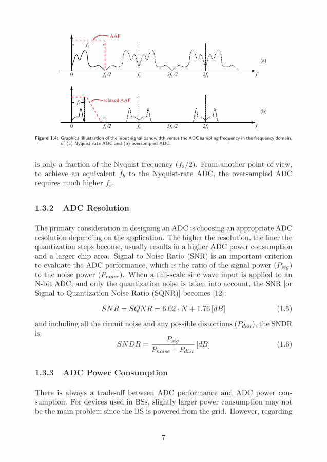
As already mentioned, before being converted to the digital domain, the analoginput signal passes through an AAF to limit its maximum signal frequency com-ponent to Nyquist frequency. It avoids any aliasing issue that high-frequencysignals folded back to fb that contaminates the original signal. For a Nyquist-rate ADC, the relation between the fb and the sampling frequency (fs) is graph-ically illustrated in Fig. 1.4 (a). It can be directly seen that the sampled inputsignal spectrum is replicated at the multiple of fs, which has to be at least twicethe fb to satisfy the Nyquist theorem.
In an oversampled ADC, the requirement of an AAF design is more relaxedthan in the Nyquist-rate ADC. The spectrum in Fig. 1.4 (b) shows that the fb
6
0 fs /2 fs
0 fs /2 fs
fb
fb
AAF
relaxed AAF
f2fs
(a)
f
(b)
2fs
3fs /2
3fs /2
Figure 1.4: Graphical illustration of the input signal bandwidth versus the ADC sampling frequency in the frequency domain,of (a) Nyquist-rate ADC and (b) oversampled ADC.
is only a fraction of the Nyquist frequency (fs/2). From another point of view,to achieve an equivalent fb to the Nyquist-rate ADC, the oversampled ADCrequires much higher fs.
1.3.2 ADC Resolution
The primary consideration in designing an ADC is choosing an appropriate ADCresolution depending on the application. The higher the resolution, the finer thequantization steps become, usually results in a higher ADC power consumptionand a larger chip area. Signal to Noise Ratio (SNR) is an important criterionto evaluate the ADC performance, which is the ratio of the signal power (Psig)to the noise power (Pnoise). When a full-scale sine wave input is applied to anN-bit ADC, and only the quantization noise is taken into account, the SNR [orSignal to Quantization Noise Ratio (SQNR)] becomes [12]:
SNR = SQNR = 6.02 ·N + 1.76 [dB] (1.5)
and including all the circuit noise and any possible distortions (Pdist), the SNDRis:
SNDR =Psig
Pnoise + Pdist[dB] (1.6)
1.3.3 ADC Power Consumption
There is always a trade-off between ADC performance and ADC power con-sumption. For devices used in BSs, slightly larger power consumption may notbe the main problem since the BS is powered from the grid. However, regarding
7

the battery-powered handheld devices, they are more favorable to utilize lowpower components.
Technology advance in the semiconductor field followed quite well with Moore’slaw, which predicted that the number of transistors in a dense Integrated Circuit(IC) doubles about every two years [19]. Thanks to Complementary Metal-Oxide-Semiconductor (CMOS) technology developments, the transistor has asmaller feature size. It benefits in a vast improvement to the circuit speed anda tremendous decrease in power consumption than the older technologies.
In recent years, 28 nm and 22 nm Fully Depleted Silicon On Insulator (FD-SOI)CMOS technologies reveal good potentials in the high-performance designs. Inthe future, the transistor size is predicted to be even smaller. The ADC designsin this research work have been implemented in 65 nm CMOS and in 28 nm and22 nm FD-SOI CMOS, trying to reach high performance and low power at thesame time. Besides, these designs utilize power-efficient architectures, trying tofurther decrease the total ADC power consumption.
1.3.4 ADC Noise
In a real circuit, noise degrades the ADC performance, causes a deviation tothe expected ADC resolution. There are two main types of ADC noise. Thefirst type is the quantization noise, which is generated during the quantizationprocess. The second type is the thermal noise related to component value,temperature, and bandwidth.
The quantization errors represent the differences between the sampled analoginput and its converted digital output, which appears to be non-linear and signal-dependent noise. These errors are generated during the quantization process,in which the sampled version of analog input is quantized and converted to aseries of digital codes with a finite resolution. The quantization errors, referredto as quantization noise, are usually modeled as uniform noise [20].
The amount of the quantization noise is directly related to the chosen ADCresolution. Theoretically, in an N-bit ADC with the number of quantizationlevels equal to 2N , the Δ represents the minimum quantization step, is:
Δ =VFS
2N(1.7)
where VFS is the full-scale voltage of the input signal. A high-resolution ADCwith a large N results in a smaller quantization step Δ. Assuming an input signal
8

has an amplitude much larger than Δ, and the quantization noise follows uniformdistribution from −Δ/2 to Δ/2, the quantization noise power PQ becomes [12]:
PQ =Δ2
12(1.8)
Obviously, PQ decreases four times when the Δ is reduced by two for every 1-bitincrease in the ADC resolution.
Besides the quantization noise limiting the theoretical limit of ADC resolution,the thermal noise is another critical design consideration in actual component-level implementation. Thermal noise in a circuit is mainly generated from therandom thermal motion of charge carriers in electrical components. The com-ponent value affects the thermal noise, such as the mean square voltage varianceper hertz of bandwidth (v2n) of a resistor is proportional to the resistance R:
v2n = 4kB · T ·R (1.9)
where kB is Boltzmann constant, and T is the temperature. When an inputis sampled on the capacitor through a non-ideal switch in the sample and holdsystem, the sampling noise is directly related to the sampling capacitance Cs.The v2n is [21]:
v2n =kB · TCs
(1.10)
Thus a sufficiently large Cs is necessary for low noise, especially in high-resolutionADCs.
There is a balance between the quantization noise and the thermal noise, suchthat too much thermal noise causes the resulting ADC resolution much lowerthan expected, while in the other case, the ADC efficiency is reduced. In apractical design, the thermal noise in an ADC could be selected comparableto the quantization noise, which may cause a slight degradation in SNDR butbenefit in a reduced chip area occupation and power consumption.
1.4 Overview of Nyquist-Rate ADCs
Nyquist-rate ADCs are attractive due to their fast speed and straightforwardarchitectures. Some of the popular Nyquist-rate ADC architectures such asFlash ADC, Successive Approximation Register (SAR) ADC, and Pipeline ADC,are shown in Fig. 1.5. These ADCs are sampled at a sampling frequency fs twicethe input signal bandwidth to satisfy the Nyquist theorem.
9
The Nyquist-rate data converters usually have a deterministic digital outputcorresponding to each of the sampled analog inputs or the so-called one-to-onecorrespondence between an analog input signal and its digitized output. Thiscategory of data converters usually does not require a sophisticated digital post-processing circuit, such as a decimation filter commonly used in oversampledADCs that will be explained in the next section.
The Flash ADC architecture, illustrated in Fig. 1.5 (a), is a fast technique thatconverts the analog input signal to a digital output. The Flash ADC usuallycomplete conversions within one clock cycle, which is a candidate architecturein building a widely used quantizer in this research work.
Despite its speed benefits, Flash ADC’s parallel conversions cause the circuitcomplexity to grow exponentially with increased resolution. Thus, achievinga high-resolution Flash ADC is difficult. Generally, to resolve N bits, 2N − 1reference voltages and a similar number of comparators are required [12]. Thecomparator outputs are thermometer code, which is hard to be directly usedexcept decoded to binary code first. An additional thermometer to binary codedecoder is required, inevitably consumes power, and occupies the chip area.
The SAR ADC is exceedingly power-efficient. It trades time for resolution,whose architecture is shown in Fig. 1.5 (b). In a typical SAR ADC, the N-bitADC resolution requires at least N+1 clock cycles to be resolved. Internally,a single comparator is used N times to compare the voltage presented at thecomparator’s input with a reference voltage. The comparator’s input voltagevaries from bit to bit, which is the voltage presented on an internal capacitorarray achieved by charge redistribution.
However, the SAR ADC suffers from limited resolution due to matching betweenthe capacitors in the physical layout and imperfections introduced by parasiticcapacitance in the capacitor array in Capacitive Digital to Analog Converter(CDAC). The non-idealities can be minimized by careful layout and furtherestimated and calibrated by digital circuits.
The third attractive ADC architecture is pipeline ADC, which converts the bitssequentially. Unlike the SAR ADCs that takes several clock cycles to converteach sample, the pipeline ADC only introduces latency between the digital out-put and the analog input signal. A typical pipeline ADC consists of severalcascaded stages, as shown in Fig. 1.5 (c). A digital logic combines all the stageoutputs to form the final digital output. For example, in stage i, digital bit biis resolved by a fast ADC (usually a Flash ADC), then converted back to theanalog domain by a Digital to Analog Converter (DAC) and subtracted fromthe input. The residue voltage is amplified by a Residue Amplifier (RA), and
10

CMP2N-1
CMP1
Vrefm
Vrefp S/H
Vin
R
R
R
R2
R2
CMPi thermometer code to binary code
decoder
Vin stage0 stagei stageN-1
digital logicNclk
S/H ADC DAC
bi
RAto next stagefrom previous stage
b0 bi bN-1
Vinclk
S/H
CMP SARcontrollogic
VrefVrefVref control signals
DoutN2N-1C C2iC C
(a)
(b)
(c)
DoutN
clk
Dout
Figure 1.5: The Nyquist-rate ADC architectures, including (a) Flash ADC, (b) SAR ADC, and (c) Pipeline ADC.
propagates to the next stage.
The limitation of a pipeline ADC is its RA, which usually has a critical accuracyrequirement. These amplifiers are sensitive to process variations that cause non-linearities in gain and offset and consume modest levels of power dissipation thatcould exceed the system’s power budget.
11

1.5 Overview of Oversampled ADCs
Another ADC category is the oversampled data converter, which includes thepopular ΔΣ ADC that employing the principle of ΔΣ Modulator (DSM). Com-pared to the Nyquist-rate ADCs, as the name implies, a noticeable difference isthat the oversampled ADC is sampled at a much higher fs for a similar fb. Thesearchitectures typically reach a high performance using moderate-resolution ana-log components, reducing in-band noise due to oversampling and noise shapingtechniques.
A simplified ΔΣ ADC linear model is shown in Fig. 1.6. The subtraction residue(Δ) of the input signal U(t) and the feedback DAC output is fed to a chain ofintegrators (whose transfer function is L) for quantization noise shaping (Σ). Inits linear model, a quantizer converts the Loop Filter (LF) output Y (t) to thedigital output V [n], with a quantization noise E(t) added in the model.
U(t)L
DAC
V[n]N
quantizer(integrators)
loop filter
Y(t)E(t) quantization
error
Figure 1.6: The ΔΣ ADC architecture.
The ADC transfer function in z-domain [11] is:
V (z) = Y (z) + E(z) = STF · U(z) +NTF · E(z) (1.11)
where the Noise Transfer Function (NTF) applies to the quantization noise andthe Signal Transfer Function (STF) applies to the signal, are:
NTF (z) =1
1 + L(z)(1.12)
STF (z) =L(z)
1 + L(z)(1.13)
Eq. 1.11, Eq. 1.12 and Eq. 1.13 indicate that the NTF is an inverse function ofthe LF’s transfer function L(z). By selecting a low-pass filter in the LF, suchas a chain of integrators, the NTF is a high-pass filter that filters E(t). Whenthe open-loop gain of L(z) is large, the STF is flat. Note that the STF can be
12

unity when an additional feed-forward path bypassing the loop filter, from U toY , is implemented.
The combination of the NTF and the STF determines the transfer function ofthe DSM. The desired transfer function is realized by selecting an appropriatearchitecture based on component-level considerations such as power consump-tion and chip area requirement.
Fig. 1.7 shows an examplar simulated ADC output spectrum of a 4th order DSMsampled at 5GHz, achieves 250MHz input signal bandwidth. The SNR is 80 dB,and noise shaping behavior is clearly visible. Note that a notch is presented atapproximately 200MHz, which is achieved by optimizing zeros in the NTF forthe maximum ADC resolution.
frequency [Hz]
[dB]
fb = 250MHz
109108107106
0
-20
-40
-60
-80
-100
-120
-140
Figure 1.7: A examplar simulated ADC output spectrum with 250MHz signal bandwidth and sampled at 5GHz.
At the ADC output, the bitstream is produced at the sampling rate, whichcontains high-frequency noise. These high-frequency noises should be filteredby a digital decimation filter to filter the out-of-band high-frequency noise anddown-sample the digital output data to Nyquist-rate [22].
1.6 Relate to State-of-the-Art ADC Designs
The state-of-the-art ADC designs are briefly discussed and compared. In theresearch area, there are two main tracks of ADC designs, namely high-speeddesigns and ultra low power designs. This research work mostly focuses onADCs that will be implemented in future high-performance base stations thusit is more favorable to high-speed ADC designs.
13

Considering the Nyquist-rate ADCs, Time-Interleaved (TI) architecture is an at-tractive technique that parallels multiple identical ADC cores at a much highersampling frequency than an individual one. Thanks to the CMOS technologynode advance which provides high-speed transistors, multi-GHz sampling fre-quency becomes possible, resulting in a signal bandwidth above 1GHz.
In ISSCC 2018, Kull et al. presented a high-speed TI ADC implemented in14 nm CMOS Fin Field-Effect Transistor (FinFET) technology [23]. The ADCwas sampled at 72GS/s and optimized for best SNDR at the Nyquist frequencyof up to 36GHz. The proposed ADC achieved 39.3 dB at low input frequen-cies and 30.4 dB at Nyquist frequency. In ISSCC 2019, Pisati et al. presen-ted a complete transceiver design implemented in TSMC 7nm FinFET CMOS[24]. The design incorporates a 7-bit 40-way time-interleaved ADC, divided intoeight front-end track and hold circuits running at 3.75GS/s. Each consists offive 750MS/s non-binary charge-redistribution DAC-based asynchronous SARADCs. The overall power consumption of the complete design is 244mW. BothADC designs show that TI architecture is a viable solution for achieving a largeinput signal bandwidth, which is also the selected technique used in SAR ADCdesigns presented in this dissertation.
The oversampled ADCs already achieved a signal bandwidth exceeding 100MHz.A ΔΣ ADC sampled at 4GHz that achieves 125MHz signal bandwidth waspresented by Bolatkale et al. in ISSCC 2011 [25], and later published in JSSC[26]. A 3rd order ADC was implemented in 45 nm CMOS, consumed 256mWenergy from dual-supply voltages 1.1V, and 1.8V and achieved 70 dB dynamicrange (DR). This work shows a good reference to my ADC design: a high-speed ΔΣ ADC tries to push circuit limits for achieving a much higher signalbandwidth using an advanced technology node.
Besides the SAR ADCs and ΔΣ ADCs, pipeline ADCs are attractive in recentyears. It is also possible to interleave multiple Pipeline ADCs. Devarajan etal. presented a 12-bit interleaved Pipeline ADC in ISSCC 2017 [27], whichis capable of being sampled at 10GS/s, achieved an SNDR of 55 dB and anSpurious-Free Dynamic Range (SFDR) of 64 dB with a 4GHz input signal. Thedesign was implemented in 28 nm CMOS, dissipating 2.9W power.
Even smartly, SAR ADCs and Pipeline ADCs can be integrated into a so-calledpipelined-SAR hybrid ADC. Ramkaj et al. presented a TI ADC with eight625MS/s channels, at a sampling rate of 5GS/s [18]. Inside each ADC channel,three dynamic SAR stages with 4-4-6 bits per stage are pipelined. The prototypeADC, fabricated in 28 nm bulk CMOS, achieved an SNDR of 61.3 dB at 600MHzand 58.5 dB at 2.4GHz and consumed 158.6mW energy. The pipeline ADCs
14

show promising results, which will be chosen as a candidate architecture forfuture designs.
In the industry, high-performance chips for high-performance applications havebeen released. In 2019, the industry’s widest bandwidth, fastest samplingrate, and lowest power consumption ADC was introduced by Texas Instru-ments (www.ti.com): a 12-bit ADC ADC12DJ5200RF, which is a dual- andsingle-channel ultra-high-speed ADC, capable to run at a sampling frequencyup to 5.2GHz, suitable for devices such as oscilloscopes, wide-band digitizers,and communications testers. The specifications of this chip are very attractive,which sets a target for future ADC designs in research.
1.7 Summaries of Experimented ADCs
In this research work, a high-speed Nyquist-rate Asynchronous SAR (ASAR)ADC has been designed. A self-generated internal clock triggers its internalcomparator sequentially. Comparing with a similar Synchronous SAR (SSAR)ADC, which was previously designed by Ericsson Research, the asynchronousversion shows a graceful SNDR degradation at the increased sampling frequency,with a small penalty in design complexity. The SSAR ADC was measured, withtheir non-idealities in the capacitor bank estimated using the post-processor inMATLAB (www.mathworks.com) and calibrated.
The oversampled ADC’s behavior and performance are evaluated by designingand implementing a high-speed ΔΣ ADC in 28 nm FD-SOI CMOS. This designtargets the application in high-performance 5G base stations. The samplingfrequency is in the GHz range with a low Oversampling Ratio (OSR) and ag-gressive noise shaping. Inverter-based integrators are used to boost the ADCspeed, and Current Mode Logic (CML) digital cells are used to improve thespeed of the digital feedback loop, with a trade-off in higher power consumptionthan a conventional digital circuit design using CMOS digital cells.
The last presented ADC design is a ΔΣ ADC implemented in 65 nm CMOS,which integrates a digital calibration core. This design aims to examine thepossibility of using an on-chip calibration core to perform background calibrationto linearize the outer-most DAC in the feedback loop.
15


Chapter 2
SAR ADC
2.1 Introduction
The rapid growth of the transmission rate in the communication systems requiresadvanced high-performance hand-held mobile devices. High-speed, medium-to-high resolution, and power-efficient ADCs are essential. The A/D convertersaccurately convert the fast varying analog signal presented at their input to adigital counterpart, achieving a high resolution and a low power dissipation atthe same time.
SAR ADC is an attractive architecture in recent years according to [13], which isvery suitable for various modern wired and wireless communication applications.The SAR ADCs incorporate power-efficient and digital-friendly architecture.The term digital-friendly means that the ADC is partially built with manydigital blocks and scales well into deep-submicrometer CMOS technology nodes.
The first commercial data converter, the vacuum-tube based “DATRAC” in1954, uses shift-programmable successive approximation architecture, achievesan 11-bit resolution in 50KS/s, and consumes a power of 500W [28]. Nowadays,state-of-the-art SAR ADCs accomplish a 13-bit resolution in 40MS/s while onlyconsuming a power less than 1mW [29]. It is a significant leap in almost a half-century.
The SAR ADC is categorized in the type of Nyquist-rate ADC. Comparing withother Nyquist-rate ADCs, the SAR ADC shows significant benefits in terms ofpower-efficiency, minimized design complexity, low chip area occupation, andhigh-speed operation.
17

Comparing with a Flash ADC, the SAR ADC consumes significantly lowerpower. In the Flash ADC architecture, N-bit resolution typically requires 2N -1comparators for a full parallel comparison with the entire quantization levels inone clock cycle. It means that the number of highly accurate comparators will bedoubled at each increased bit. On the contrary, in the SAR ADC, the increasedresolution only requires an increased number of accurate and well-matched com-ponents, e.g., twice the number of capacitors for an extra bit. Even includingthe additional switches necessary to control those added capacitors, the wholedesign complexity does not increase exponentially.
Comparing with the Pipeline ADC, the SAR ADC does not show large latencyas the Pipeline ADC usually does. Latency means a time delay between thesampled voltage and its corresponding digital output value. It is the nature of aPipeline architecture since it has inherent parallelism to utilize each stage sim-ultaneously. Furthermore, the SAR ADC does not require the high-performanceinter-stage amplifiers as needed in the Pipeline ADCs. The high linearity andlow noise amplifiers between the stages contribute to increased power consump-tion and increased circuit complexity, limiting the maximum circuit speed.
In short, the SAR ADC divides the bit conversions into several conversion stagesby using a single comparator approximately N times for N-bit resolution.
This chapter focuses on the theory and the circuit implementations of two prac-tical SAR ADC designs: an SSAR ADC and an ASAR ADC. Their archi-tectures are explained, and the differences in clocking schemes are shown. InSection 2.2, a basic SAR ADC architecture is shown, and the Successive Ap-proximation (SA) algorithm is briefly explained. Section 2.3 shows a TI SARADC architecture, which has great potential in increasing the ADC signal band-width. Then, Section 2.4 discusses the synchronous and asynchronous clockingscheme. Section 2.5 explains the component-level implementations of the ASARADC designs, with the comparator, CDAC, and SAR control logic explainedin detail. Lastly, in Section 2.6, the SAR ADC non-idealities, introduced byProcess-Voltage-Temperature (PVT) variations, will be addressed. Techniquesto improve the SAR ADC robustness are presented, including redundancy tech-nique, CDAC array imbalance estimation and calibration, ASAR ADC internalclock pulse width tuning, and a proposed design method to reduce SSAR ADCrandom noise when incorrect bit conversions occur.
18

2.2 SAR ADC Architecture
The SAR operation, as the name implies, converts the analog input signal to anequivalent digital output based on the SA algorithm. The SA algorithm is animplementation of binary searching, realizing N-bit resolution by N comparisons.Many of the SAR ADCs nowadays incorporate the operation principle similarto the charge redistribution technique described in [30], using a binary-weightedcapacitor array to perform high-speed conversion.
The SSAR and ASAR ADC architectures share numerous similar internal com-ponents but differ in the control logic design. Fig. 2.1 shows a conceptual 6-bitSAR ADC architecture using a synchronous clocking scheme. In this particu-lar SAR ADC architecture, four main components are shown: a S/H circuit, aCDAC, a comparator (CMP), and a SAR control logic. An external clock clkcontrols the comparator and the SAR control logic. The comparator makes com-parisons at the clk falling edge, and the SAR control logic sequentially generatesdigital outputs b5 to b0 at the clk rising edge.
Vin
clk
0
b5 b4 b3 b2 b1 b0digitaloutput
>0
<0
>0>0 >0
<0
Vin_init
CDAC CMPVinS/H
control signalsmp
b5
b0
digitaloutput
analoginput Vin_init
timing diagram
registerSAR
controllogic
-
+
MSB LSB
bootstrapped
smp
clk
Figure 2.1: A 6-bit SAR ADC conversion example, with the timing diagram illustration of the ADC input and outputsignals.
To facilitate understanding the SA algorithm, the timing diagram of externalclock signal clk, sampling signal smp, comparator input voltage (also the CDACoutput voltage) Vin, and six digital output bits b5 to b0 are shown in the bottompart of Fig. 2.1. The algorithm finds a unique digital code representing the
19
sampled input voltage Vin init, marked in the red dot in the timing diagram. Inthe sampling mode, the analog input voltage is sampled on the binary-weightedcapacitors in the CDAC. In the hold mode, the sampling signal smp is released,and the Vin = Vin init is proportional to the sampled input voltage. Next, bitconversions start.
At a first clk falling edge, Vin is compared with a reference voltage (0 in thisexample). When Vin > 0, the comparator output is a logic one, and vise versa.Next, the comparator output is latched by the SAR register at the clk risingedge, which determines the Most Significant Bit (MSB) (b5) in the digital out-put. In the meantime, the control logic sets a set of control signals based onthe comparison result to redistribute the charge in the CDAC, causing the Vin
increases or decreases to a new value accordingly, in a step half of the previ-ous step. The same procedure continues until the Least Significant Bit (LSB)conversion is completed. The bits determined during each conversion step arecombined as the ADC digital output.
The S/H, placed at the front of the ADC, samples the analog input voltage togenerate a series of sampled voltage (Vin init). The linearity of the S/H blockis essential since any non-linearity introduced by the S/H directly propagatesto the ADC output. Typically, the S/H component-level design is based on thebootstrapped architecture, an architecture initially proposed in [31]. The boot-strap technique allows a constant voltage applied to the sampling transistor’sgate-to-source terminals, allowing a low and constant conducting resistance in-dependent of the input signal voltage. Therefore, the sampling switch introducesminimum distortion to maintain the overall SAR ADC linearity.
The CDAC follows the S/H, constructed by an internal capacitor array of ca-pacitors with binary-weighted capacitance. The controlling scheme and chargeredistribution details will be explained in Section 2.5.1.
The comparator is a crucial component in a SAR ADC. Noise, offset, and com-parison speed of the selected comparator design dominant the SAR ADC per-formance, thus requires a trade-off between its performance and power consump-tion.
Lastly, the SAR control logic latches the comparator outputs. Its primary func-tion is to generate a series of control signals for the switches in the CDAC ineach clock cycle, connecting the corresponding capacitor to one of the referencevoltages to redistribute charge stored on the capacitors. In the meantime, thecomparison results are saved in the registers in the SAR control logic, becomingthe SAR ADC digital output.
20

2.3 TI SAR ADC Architecture
The high-speed, high-resolution ADCs commonly incorporate TI architecture.It is a practical method that interleaves multiple SAR ADCs for increased per-formance, satisfying a broad signal bandwidth requirement and a fast samplingrate. In the TI ADC architecture, each of the single SAR ADC is called asub-ADC core. The sub-ADC core specification is chosen such that an optimumpoint is reached between the total ADC power consumption versus the samplingrate.
Fig. 2.2 shows a 7-channel TI SAR ADC architecture. A timing diagram isexplicitly shown at the lower-left corner to illustrate the sampling signal timingdifferences between the common S/H and the sub-ADC cores. The common S/His clocked by a sampling signal smp, which samples the buffered analog inputsignal to be Vsmp, then distributes to all the sub-ADC cores. The sub-samplersin the sub-ADCs are clocked in turn, sample the Vsmp to be Vin init by non-overlapped sampling signals smp0 to smp6, each with a pulse width equal toone smp period. Thus, at a time, only one of the sub-ADCs is in the samplingstate while the rest are in bit conversions. The seven sub-ADC core outputsare sequentially selected by a digital multiplexer. The TI-ADC digital outputis generated at a rate of fs for further signal processing in the digital domain.
...
common
input...
sub-ADC0
digitalmultiplexer
sub-sampler
smp0smp1
smp6
G
buffer
smpsmp
smp6
smp1
smp0
...
S/Hanalog
outputsub-sampler
sub-sampler
input
sub-ADC1
sub-ADC6
Vsmp
Figure 2.2: Time-Interleaved ADC architecture, with sampling signals timing diagram shown at the lower-left corner.
There could be a trade-off in selecting the sub-ADC core bandwidth and thenumber of sub-ADC cores. In many of the TI ADC designs, the single sub-ADCcore has a minimum 10-bit resolution and a sampling frequency of 200–300MS/s.For example, in [32], a 10-bit non-interleaving SAR ADC design is presented,which achieves an SNDR at Nyquist frequency of 57.7 dB at 160MS/s and57.1 dB at 320MS/s.
Interleaving a small number of high-performance sub-ADCs becomes a sensiblechoice in wide-bandwidth designs. The total number of sub-ADC cores is re-
21

duced, but each sub-ADC core’s sampling rate is increased. It is beneficial interms of matching between sub-ADC cores and a simplified calibration module.The work in [33] presents a high-speed single SAR ADC running at a samplingrate of 1.25GS/s, which still maintains an SNDR of 36.4 dB up to 5GHz in-put frequency, allowing smooth integration into a future interleaved system.However, a single ADC core only achieves a resolution of 7-bit, it is not verysuitable for a TI-ADC requiring a higher resolution. The TI SAR ADC couldalso have a large number of sub-ADCs interleaved for an even higher samplingrate. For example, in [34], a 16-channel TI SAR ADC has been presented witha 10-bit resolution and a sampling rate of 2.6GS/s, which achieves an SNDR of50.6 dB at Nyquist frequency; in [35], a 12-bit 8-way time-interleaved SAR ADChas been designed, achieving an SNDR above 65.3 dB at 1GHz input frequencyunder a sampling rate of 1.6GS/s.
2.4 SAR ADC Clocking Schemes
One of the key differences between the two types of SAR ADCs is their clockingschemes. Specifically, the term synchronous or asynchronous is used to describewhether or not the SAR ADC internal blocks are synchronized to an externalclock. If the SAR ADC internal states are updated synchronously with theclock cycles, it is an SSAR ADC. On the other hand, if the internal states arechanged depending on the status of the internal comparator decision and aninternal clock generated upon the completion of the previous comparison, it isan ASAR ADC.
Both architectures have benefits and drawbacks, with trade-offs among the per-formance, power consumption, and design complexities. In the following Sec-tions, the SSAR ADC is described first, followed by the detailed explanationsof ASAR ADC.
2.4.1 Synchronous SAR ADC Clocking Scheme
The SSAR ADC is clocked by a high-speed external clock signal clk possiblyrunning at the GHz frequency range. Such a high-speed clock is distributed toall the internal blocks, provides synchronization of the internal blocks. Thus,digital-friendly SAR control logic can be designed, attracting interests both incommercial applications and research [23].
However, a potential risk for the SSAR ADC is an insufficient decision time
22

for the comparator to complete a comparison. If the clock is fast and an errorappears on deciding a high-weight bit, the resulting performance may degradeabruptly. Thus, the external clock frequency has to be slow enough to fulfill theworst-case scenario, which significantly limits the maximum speed of the SSARADC.
Fig. 2.3 shows a simplified SSAR ADC architecture. The illustration is single-ended, but the real implementation has a differential architecture. The timingdiagram of the sampling signal smp, the digital output bN−1 to b0, and theexternal clock clk, are shown. It can be seen from Fig. 2.3, that at least N + 1clock cycles are required for a complete N-bit conversion, where one clock cycleis used for sampling, and the rest N clock cycles are occupied for bit conversions.Note that there is one clock cycle latency due to the comparator output beenlatched by the SAR register at the upcoming clock rising edge.
bN-1 bN-2 b0
analog
clk (external signal)
CDAC
CMP
S/H
control signalsmp
SSAR ADC
-
+input bN-1
b0
digitaloutput
registerSAR
controllogic
bit conversionssample latency
MSB MSB-1 LSB
clk
smp
digitaloutput
Figure 2.3: N-bit SSAR ADC architecture and critical nodes timing diagram.
The SSAR benefits from a structural digital-cell-based SAR control logic designbut also has a few drawbacks.
� The SSAR ADC could consume high power and require a complicatedlayout to distribute a high-speed external clock (clk). At an increasedADC resolution, multiple clock cycles are needed to complete a singlesample conversion. The clk frequency could be up to a few GHz, whilethe sampling frequency fs is only in a few hundred MHz range. It showsthat buffering such a high-frequency clock signal requires a large amountof power to be dispensed, which is higher than only buffering fs in anASAR ADC counterpart. Besides, such a high-speed external clock signal
23

distribution in the chip layout requires design experiences. Any clockdelay between the comparator and the control logic may affect the circuitfunctionality, which must be well controlled. Thus, a general rule is todraw the layout routes as short as possible and match the critical clockroutes length.
� The SSAR suffers an inefficient clock cycle utilization. Since the externalclock signal to the SSAR ADC has a fixed clock cycle, it becomes lessefficient in clocking the ADC since the comparator decision time is in-put voltage dependent. Previous works pointed out that the comparatordecision time versus comparator input voltage follows a logarithm func-tion as described in [36]. The maximum clk frequency has to satisfy theworst-case scenario, i.e., a very long comparator decision time when thecomparator experiences a minimum input voltage. Thus, the maximumSSAR ADC sampling frequency is limited since it is usually proportionalto the external clock frequency.
2.4.2 Asynchronous SAR ADC Clocking Scheme
Alternatively, to utilize the clocking more efficiently, a similar ASAR ADC isdesigned. The scenario becomes different when an asynchronous clocking schemeis used. The ASAR ADC architecture, shown in Fig. 2.4, is similar to the SSARADC architecture in Fig. 2.3, but differs in clocking scheme. A low duty cycleexternal sampling signal smp, with a frequency of a few hundred MHz, controlsthe start time of each sample conversion. Internally in the ASAR ADC, thebit conversions are converted by the quantizer clocked by a self-generated high-speed clock cmp clk from the ASAR control logic. The ASAR ADC robustnessis significantly improved compared to the SSAR ADC since the dynamic clockguarantees each bit conversion finished before the start of the subsequent bitconversion. Any bit conversion error caused by insufficient timing will onlyappear to the low-weighted bits in a sample that causes marginal performancedegradation. Furthermore, it avoids the necessity of directly injecting a high-speed external clock into the ADC, which saves power and avoids any potentialtiming issues.
In summary, the ASAR ADC only requires an external low frequency samplingsignal clocking the ADC, which consumes less power in buffering it, therefore,showing a better power efficiency. It is a preferable choice as a high-performancesub-ADC core to be further used in a time-interleaved way.
The benefits of selecting an ASAR ADC over an SSAR ADC counterpart are
24

cmp_clk
smp
bN-1 bN-2 b0
analog
smp (external signal)
CDAC
CMP
S/H
control signalASAR ADC
-
+input
digitaloutput
registerSAR
controllogic
bit conversionssample
digitaloutput
MSB MSB-1 LSB
cmp_clk
gap
ready
ready
b1
bN-1
b0
Figure 2.4: N-bit ASAR ADC architecture and critical nodes timing diagram.
two-fold:
� Buffering and distributing the external high-speed clock signal as in theSSAR is alleviated. Instead, a much slower sampling signal smp is distrib-uted to both the S/H block and the ASAR ADC control logic. Distributingand buffing the smp to the ASAR ADC consumes much less power thanthe high-frequency clk to the SSAR ADC. In the meantime, reduce thelayout complexity as well as the chip size.
� The ASAR ADC is generally faster than the SSAR ADC. The prior work[36] claims that the asynchronous conversion takes advantage of the fastercomparison cycles since there is only one critical bit conversion with aworst-case comparator decision time. It proves mathematically that thetotal conversion time in the ASAR ADC is shorter than the SSAR ADCcounterpart. The difference becomes more pronounced when the ADCresolution is high, which means more bits need to be converted.
Above all, the ASAR ADC dynamically utilizes the bit conversion time slotas the timing diagram example illustrated in Fig. 2.4. Because the comparatordecision time depends on its input voltage, the clock pulse widths can be dy-namically adjusted in the ASAR ADC to match the conversion time of eachbit for maximum efficiency. Therefore, an important task is to understand thecomparator behavior. The comparator will be studied in Section 2.5.3 where theinput voltage versus the comparator decision time is studied in detail supported
25

by the results from component-level simulations. In the next section, the timingdifferences between the two architectures are analyzed first.
2.4.3 SSAR and ASAR ADC Timing Differences
The timing differences of the SSAR and the ASAR ADC have been brieflyexplained in the previous Sections, where the N-bit SSAR and ASAR ADCarchitectures and their timing diagrams were illustrated in Fig. 2.3 and Fig. 2.4.In this section, the timing differences between the two ADC architectures areanalyzed mathematically.
Fig. 2.5 (a) and (b) show the detailed timing diagram of the SSAR and theASAR ADC, respectively. The key controlling signals i.e., clk, smp, cmp clk,and ready, are marked in bold. The sampled analog input voltage Vin init thatapplied onto the CDAC is assumed to be equal in the two timing diagrams. InFig. 2.5, τk denotes the comparator decision time for kth conversion (where kranges from N-1 down to 0), and T is the clock period of the external clocksignal clk to the SSAR ADC. The tdac is the time allocated for CDAC chargeredistribution, and the tsmp is the sampling signal width, lasting one clock cycleT and are aligned between the two designs. The comparator differential inputvoltage is denoted as Vin (=Vinp − Vinm), and its differential outputs are doutpand doutm.
...
...
...
tsmp ...
...
...
N-1 N-2 01
N
tsmp T T T T T
tdac tcmp
N-1 N-2 01
tdac
tdac+
Vin_init
bN-1 bN-2 ... b0b1b2b3
bN-1 bN-2 b0b1b2...
...
(a)
(b)
Vin_init
...
...
tSSAR
smp
tASAR
ASA
R A
DC
SSA
R A
DC
clk
Vin
cmp_clk
doutp( (
Vindigitaloutput
digitaloutput
ready
N-1+ N-2 + 0...+
doutm
doutp( (doutm
Figure 2.5: The timing diagram of (a) an SSAR ADC and (b) an ASAR ADC.
26

The bit conversions start after sampling. The Vin init is the first voltage to becompared, and the comparison result determines the MSB bit bN−1 value. Therest bit (bN−2 to b0) are converted following the direction from MSB to LSB,described below:
� A new Vin is loaded onto the CDAC, in response to the previous (k+1)th
bit conversion. At the same time, comparator outputs doutp and doutmare reset to 0. In the SSAR ADC, the length tdac of this phase is half theperiod T of the clock clk, which is tdac ≈ 120 ps under nominal workingconditions based on simulation results.
� The value of the kth bit is decided: doutp and doutm are resolved at thefalling edge of cmp clk after a signal-dependent decision time τk.
In the SSAR ADC, the decision time is typically fixed to tcmp, which is equalto one half of T , independent of k. To cope with the metastability errors, tcmp
should be long enough to cover all but the most extended decision times. Theconversion time tSSAR of the N-bit SSAR ADC is then:
tSSAR = N · (tdac + tcmp) + tsmp = N · T + tsmp (2.1)
where tsmp is the time allocated for sampling analog input into the ADC.
In the ASAR ADC, the conversion time tASAR is instead:
tASAR = N · tdac + ttot + tsmp (2.2)
with ttot in each sample:
ttot =N−1∑k=0
τk (2.3)
The ASAR ADC is faster than the SSAR ADC if the ttot is smaller than theN · tcmp, which is valid in most situations.
2.5 Component-Level Implementations
Both the SSAR and ASAR ADCs have been implemented in 22 nm FD-SOICMOS and tested. The architectures of both SAR ADC designs are shownin Fig. 2.6. Note that the designs implement differential architectures to re-duce even-order distortions. One of the CDAC architecture is drawn explicitly
27

to show the controlling switches and their corresponding control signals gener-ated by the Asynchronous Control Logic (ACL). The two designs share similarhardware blocks, e.g., similar CDAC and comparator, but different in the SARcontrol designs. In the SSAR ADC architecture shown in Fig. 2.6 (a), the ex-ternal clock signal clk ext is buffered before clocking the comparator and theSynchronous Control Logic (SCL). On the contrary, in the ASAR ADC archi-tecture shown in Fig. 2.6 (b), a low duty cycle external sampling signal smp extis buffered and then sent to the ACL. As mentioned earlier, a series of dy-namic clock pulses cmp clk are generated to trigger the comparator for makingdecisions.
... ...Cb
Cm-1CC1 Ci
data(m-1:0)
(a)
(b)
Control Logic (SCL)
Synchronous
(1(()1 (1(()1 (1(()1
CMP
c d d
i+1
data(m-1:0)
Control Logic (ACL)
BUF
BUF
SW1 SWi SWi+1 SWm-1
(i(()i (i(()i (i(()ic d d (i((+1)))1
(i((+1)))1
(i((+1)))1
c d d (m((-1))1
(m((-1))1
(m((-1))1
c d d (
CDACCDAC
CDAC
CDAC
Ainp
clkclk_ext
smpc;d;d
c;d;d
smp_ext
smpcmp_clk
readyVinm
Ainm
Vcm
Vref+ Vref-Vcm
Vcm Vcm
Vcm
CMP
Asynchronous
Vref+ Vref-VcmAinp
Vref+
Vref-
Ainm Vref+ Vref- Vcm Vref+ Vref- Vcm Vref+ Vref- Vcm Vref+ Vref-
Vinp
doutm
doutpVinp
Vinm
doutm
doutp
Figure 2.6: Component-level implementation of (a) m-bit SSAR ADC and (b) m-bit ASAR ADC, with one of the CDACexplicitly drawn.
In the following sections, the power-efficient CDAC design with split-capacitorarray architecture and Merged Capacitor Switching (MCS) switching schemewill be described, and the bridge capacitor value (Cb) will be mathematicallycalculated. The comparator design will be described, and both the SCL and theACL designs will be presented in detail.
2.5.1 CDAC Design
The CDAC is a vital component dominating the SAR ADC performance. TheCDAC has to be well-matched without creating linearity issues to the ADCperformance. In this section, the binary-weighted CDAC is firstly explained forillustrating the CDAC operation principles. A split-capacitor CDAC design isthen shown, which uses a reduced total capacitance for the same ADC resolution.
Fig. 2.7 (a) shows a single-ended binary-weighted N-bit CDAC with bottom-
28

plate sampling. The capacitor array consists of switchable binary-weighted ca-pacitors. It is implemented by an integer number of unit capacitance Cu, whichis beneficial in terms of the device matching. There is an extra Cu connectedto the ground, resulting in a total capacitance in the CDAC equal to exactly2N−1 · Cu.
2Cu
Cb mDAC
(b)
Ce 2BS-2Cu 2BM-1CuCu
(a)
Vref+ Vref-Ain
smp
To comparator
Cu 2Cu 2N-2Cu... 2N-3Cu
smp
Cu
binary-weighted capacitor array
smp c2 d2d2 smp cN-1dN-1 dN-1
sDAC
4Cu... ...
To comparator
Vref+ Vref-
smp cN-2dN-2 dN-2c1 d1d1
Vref+ Vref- Vref+ Vref-
Figure 2.7: The CDAC architecture of (a) a bottom plate sampling binary-weighted CDAC and its controlling switches,and (b) a split capacitor array with a bridge capacitor Cb between the mDAC and the sDAC.
The switches for controlling the capacitors array are drawn explicitly in Fig. 2.7(a), with connections to either the input Ain (=Ainp − Ainm) during samplingor to the reference voltages during bit conversions. The reference voltages areground, plus (Vref+), and minus (Vref−) reference voltage. The ith capacitor’sconnection for the ith bit conversion is depended on the control signals c(i),d(i), and ¯d(i). The CDAC utilizes bottom plate sampling, which provides goodsignal isolation between the input and the comparator.
In the binary-weighted CDAC design, the total capacitance grows exponentiallywith the increased ADC resolution. An efficient way of reducing the total capa-citance is implementing a split-capacitor array [12], as shown in Fig. 2.7 (b). Inthe architecture, a small bridge capacitor Cb is placed between the main-DAC(mDAC) and the sub-DAC (sDAC) as an attenuation capacitance. It reducesthe total capacitance by approximately half compared to the binary-weightedCDAC array while agreeing with the SA algorithm. Since the total capacitanceis reduced, the split-capacitor CDAC architecture shows a decreased ADC powerconsumption and reduced chip area than the binary-weighted CDAC.
During sampling, the sampling switches controlled by sampling signal smp are
29

closed. The input signal is applied to the capacitor bottom plates. The bitconversions start after sampling when the sampling switches are opened, causingan initial voltage Vin init appears at the CDAC output. The charge stored on theCDAC capacitors are redistributed in the following bit conversions, governed bythe control signals c, d, and d from the SAR control logic, resulting in a changeto the CDAC output voltage.
There are multiple switching schemes to efficiently redistribute CDAC chargesin response to the c, d, and d. In the conventional switching method presented in[37], there are a series of up and down transitions for the CDAC to redistributethe charge. The prior work [38] claimed that the down transitions consumealmost five times higher the power than the up transitions, which makes theconventional algorithm insufficient. It presented a method to split an MSBcapacitor into binary scaled sub-capacitors, which achieves an average switchingenergy reduction of 37% compared with the conventional switching algorithm.However, it is still less efficient than the MCS scheme presented in [39] and [40],which is 93.4% more power-efficient than the conventional switching scheme.Briefly, in the MCS switching scheme, the capacitor bottom plates are firstconnected to the input Ain in the sampling phase, then to the common-modevoltage in a differential architecture. The reversed polarity Ain now appearsat the CDAC output for the MSB to be converted. Afterward, each capacitorbottom plate is connected to either Vref+ or Vref− depending on the previous bitconversion, until the LSB capacitor is switched. Using three reference levels inthe MCS scheme instead of two in the conventional method, the average CDACswitching power is significantly reduced.
To further analyze the split-capacitor CDAC, a complete 10-bit split-capacitorarray is drawn in Fig. 2.8 (a). The CS in sDAC and the CM in mDAC are chosento be equal weight for the Pseudo-Random Bit Sequence (PRBS) signal injectionfor calibration purposes, which will be explained in Section 2.5.2. Fig. 2.8 (b)shows a simplified capacitor array, where the capacitors except CS and CM arecombined into CSe in sDAC and CMe in mDAC.
Each capacitance is preferably chosen as an integer number of unit capacitanceCu to improve the matching between components in an actual design. In theproposed split-capacitor architecture, Cb is an integer number of Cu, while theCe is set accordingly. It was shown that to set Cb = 2Cu [41], or even simplyCb = Cu [42] is possible for a linear transfer function.
To derive a relation between Cb and the other capacitances, the inverse polarityvoltage −V and +V act on the CS and CM , respectively. A Norton equivalentcircuit is used, which is shown in Fig. 2.8 (b).
30
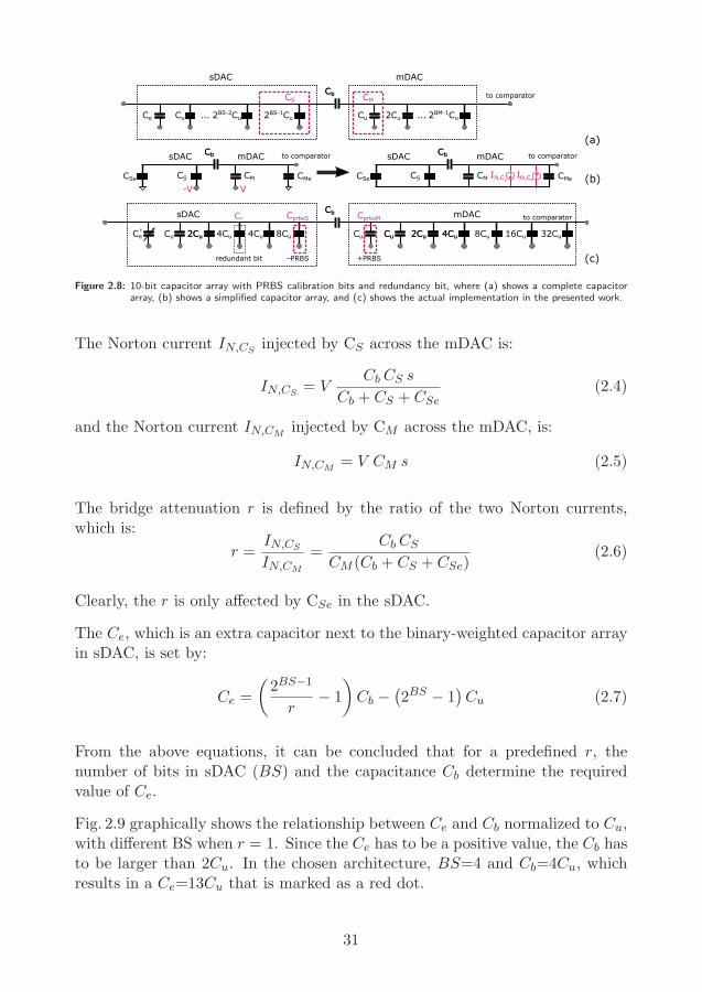
IN,CMIN,CS
Cu 2Cu 4Cu Cu 2Cu 4Cu
Cb
2Cu Cu 2Cu 4Cu
Cb mDACsDAC
CMe
Cb
CSe CS
Cb mDACsDAC
(c)
8Cu
redundant bit
4Cu Cu 8Cu 16Cu 32Cu
CM
CprbsS CprbsMCr
2Cu
Cb
Cu
Cb
mDACsDAC
to comparator
(a)
Ce 2BS-2Cu 2BM-1Cu
CMCS
...
to comparator
Cu ... 2BS-1Cu
Ce'
V
+PRBSPRBS
(b)-V
to comparator
CMe
Cb
CSe CS
Cb mDACsDAC
CM
to comparator
Figure 2.8: 10-bit capacitor array with PRBS calibration bits and redundancy bit, where (a) shows a complete capacitorarray, (b) shows a simplified capacitor array, and (c) shows the actual implementation in the presented work.
The Norton current IN,CSinjected by CS across the mDAC is:
IN,CS= V
CbCS s
Cb + CS + CSe(2.4)
and the Norton current IN,CMinjected by CM across the mDAC, is:
IN,CM= V CM s (2.5)
The bridge attenuation r is defined by the ratio of the two Norton currents,which is:
r =IN,CS
IN,CM
=CbCS
CM (Cb + CS + CSe)(2.6)
Clearly, the r is only affected by CSe in the sDAC.
The Ce, which is an extra capacitor next to the binary-weighted capacitor arrayin sDAC, is set by:
Ce =
(2BS−1
r− 1
)Cb −
(2BS − 1
)Cu (2.7)
From the above equations, it can be concluded that for a predefined r, thenumber of bits in sDAC (BS) and the capacitance Cb determine the requiredvalue of Ce.
Fig. 2.9 graphically shows the relationship between Ce and Cb normalized to Cu,with different BS when r = 1. Since the Ce has to be a positive value, the Cb hasto be larger than 2Cu. In the chosen architecture, BS=4 and Cb=4Cu, whichresults in a Ce=13Cu that is marked as a red dot.
31

1 2 3 4-2 0
-1 0
0
1 0
2 0
3 0BS =3BS =4BS =5
r =1
Cb [normalized to Cu]
Ce
[nor
mal
ized
to C
u]
Figure 2.9: The relationship between Ce and Cb in different BS in the proposed 10-bit capacitor array, normalized toCu.
In the proposed CDAC architecture, parts of the capacitors are used for addingan extra bit for redundancy. The redundancy scheme that will be explained inSection 2.6.5 is a practical way to reduce the errors introduced by slow CDACsettling time in particular bits. Therefore, 4 out of 13 Cu from Ce are occupiedfor capacitors implementing redundant bit. As a result, the actual extra capa-citance C ′
e is 9Cu, and the actual CDAC implementation is shown in Fig. 2.8(c).
2.5.2 Estimation and Calibration of CDAC Imbalance
This part explains the estimation and calibration of the split CDAC array imbal-ance. The capacitor matching can be ensured by layout matching in sDAC andmDAC, respectively. However, the parasitic capacitance introduces a weightimbalance between the two CDAC arrays, leading to performance degradation.
A practical way to balance the two capacitor arrays is by injecting PRBS to thesame weighted capacitor in both sides of the capacitor bank and examine theiroutputs. Still consider the CDAC array shown in Fig. 2.8, where the CprbsS andCprbsM on each side of the DAC array are two equal weights capacitors, whenr = 1. Ideally, without parasitic capacitance, the test sequence will not be visibleat the output since the Norton equivalent current IN,CS
, and IN,CMare canceled
out. However, influenced by DAC imbalance due to parasitic capacitance in thesDAC, the test sequence residue may appear at the SAR ADC digital output.The characteristic of the DAC arrays is determined by post-processing, namely,using correlation to detect the residue value and estimate the weight differencebetween sDAC and mDAC.
The post-processor finds the correlation between the known PRBS signal (SPRBS)
32

and the ADC output (So). Its output is proportional to the deviation Δr fromthe ideal value of r. The estimated r of the bridge attenuation is:
r = 1 +Δr = 1 +1
wM
M∑k=1
So[k]SPRBS [k] (2.8)
where M is the number of samples and w is the PRBS bit weight.
To calibrate the CDAC, it is preferable to use r directly switching on or off afraction of C ′
e on-chip, which is made tunable by digital control signals; altern-atively, the SDAC bit weights can be corrected in the digital domain throughmultiplication by r, then combined with the MDAC bits.
Fig. 2.10 plots r vs. C ′e between 3 and 15Cu, where its nominal value is 9Cu. In
the first scenario shown in blue curve, the r is implicitly given by Eq.2.7. In thesecond scenario shown in green curve, the r is estimated using Eq.2.8. Lastly,r is swept and found when maximum SNDR is reached, shown in purple curve.From the simulation, the three methods generate nearly identical results.
4 6 8 10 12 14C
0.8
0.9
1
1.1
1.2
e
estim
ated
r
r: theoreticalr: by estimatorr: by sweep
'9
[normalized to Cu]
Figure 2.10: Theoretical r values, estimated value by the correlation-based estimator, and estimated value by SNDRmaximization sweep, as a function of C′
e. Capacitor values are normalized to Cu.
2.5.3 Comparator Design
In a SAR ADC, another core component is a comparator. The comparatorcompares its input voltage Vin with a reference voltage (zero in the single-endedillustration) to generate a digital logic value based on the comparison result.Specifically, the Vin, which is also the CDAC output voltage, varies in each con-version step in response to a previous bit decision. In the following examples,
33

assume logic one is generated when the Vin is positive, and a logic zero is gen-erated when the Vin is negative or zero.
2.5.3.1 Comparator Component-Level Implementation
In the component-level implementation, a simplified differential dynamic com-parator schematic is shown in Fig. 2.11. The circuit is similar to the designpresented in [43], which consists of a clocked pre-amplifier, a regenerative latch,and an output stage. Note that there are two choices of the output stages: eitheran SR latch or simply two buffers.
SR latch
pre-amplifier
clk
VinpVinm
Vampm
VamppVlatchmVlatchp doutm
doutp
buffersdoutmdoutp
clkVampp
reset conversion
regenerative latch
tconv
Vampm ready
Figure 2.11: Comparator schematic with either an SR latch or two buffers in its output stage.
The timing diagram of the clk and the pre-amplifier output signal Vamp is drawnat the lower-left corner in Fig. 2.11. At the clk high pulse, the pre-amplifier is inreset. Both of the pre-amplifier outputs Vampp and Vampm are reset to ground,which resets the regenerative latch internal nodes and removes any memoryeffect from the previous bit conversion. At the clk low pulse, the comparator’sdifferential input voltage Vin is amplified to toggle the regenerative latch.
The pre-amplifier schematic is drawn in Fig. 2.12, including a clocked amplifystage and an inverter second stage to increase gain. There are an optional inputpair of P-Channel Metal-Oxide-Semiconductor (PMOS) transistors drawn inthe blue dashed box, behaving as a push-pull architecture together with theN-Channel Metal-Oxide-Semiconductor (NMOS) transistor pair, to reduce thecomparator noise. However, the input capacitance is increased, which slightlyaffects the Vin transition speed.
There are two options at the comparator output stage: either an SR latchor merely a pair of buffers. By implementing an SR latch, the comparator
34

VampmVinp
clk
Vampp
Vinm
Vinp Vinm
PMOS input pair
inverter stage
clk
clkclkclk
clk
vdd vdd vdd
Figure 2.12: Pre-amplifier schematic, used in the comparator.
outputs doutp, and doutm are stable for a whole clock period [44], which eases thefollowing control logic design. However, it may experience bit conversion errorsdue to a remained previous bit conversion: the previous comparator decisionis not updated in time due to a short clock cycle period before latched by thefollowing SAR control logic. By replacing the SR latch with two buffers forthe differential output terminals, the doutp and doutm switch exactly as theregenerative latch’s outputs Vlatchp and Vlatchm. In other words, the comparatoroutputs doutp and doutm exercise a reset pulse before becoming valid.
A benefit of replacing the SR latch with buffers is that reset values are alwaysused instead of the remaining previous decisions whenever comparator decisionsare not ready. It will no longer randomize the bit decisions but instead set themto a default value. Equivalently, the default decisions create a high ADC offsetvoltage, showing an increased Direct Current (DC) offset to the ADC outputspectrum and a reduced ADC dynamic range. More importantly, the ADC willnot suffer a significant performance drop. Another benefit of removing the SRlatch is that the comparator becomes faster, since the SR latch’s cross-coupledarchitecture inevitably introduces a small propagation delay to the output sig-nals.
2.5.3.2 Comparator Decision Time
The comparison speed is one of the dominant factors limiting the maximumSAR ADC conversion speed, which is studied in detail in this section.
In an actual circuit, the comparator decision time τ is not a constant value. It issignal-dependent and is directly related to the Vin. Fig. 2.13 shows a conceptualtiming diagram of the regenerative latch, in which differential input Vin and two
35

outputs Vlatchp and Vlatchm are shown. For illustration purposes, the regenerativelatch generates Vlatchp and Vlatchm within a finite decision time τA = 36 ps for alarge Vin (100mV) and τB = 74 ps for a small (100 uV) Vin, where both decisiontimes are derived from component-level simulations.
clk
Vlatchp
Vlatchm
Vin=100uVVin=100mV
B=74ps
A=36ps
time
Figure 2.13: Regenerative latch timing diagram for a 100mV and a 100 uV differential latch input voltage Vin.
Based on the discussions presented in [45], the dependence of τ on Vin is ex-pressed by a logarithm equation, which is:
τ = f(Vin) = α ln(Vin) + β (2.9)
where α and β are constants, determined by the selected components and com-parator architecture.
The component-level comparator, whose schematic was already shown in Fig. 2.11,is simulated in 22 nm FD-SOI CMOS. A τ versus Vin plot is drawn in the redcurve in Fig. 2.14. Besides, the ideal calculation using Eq. 2.9, with α = −3.5 psand β = 70 ps, is plotted in the blue dashed curve. A trend is clearly visible: ata very small Vin, the τ is very large. With the Vin continuously increasing, theτ reduces.
VMW
tconv
increased
decreased
0 0.2 0.4 0.6 0.8 1normalized Vin
65
70
75
85
80
bit c
onve
rsio
n tim
e (
) [ps
]
90
95
100
component-level comparator =(-3.5ps) ln(Vin)+70ps
metastabilitywindow
Figure 2.14: τ vs. input voltage Vin, in a component-level comparator and an ideal comparator model.
36

The fully-differential comparator architecture has symmetrical plus and minussignal paths. Ideally, with a small input voltage Vin ≈ 0, the clocked pre-amplifier outputs are very close to each other. The slight voltage difference isnot sufficient to drive the regenerative latch, causing a long decision time for afull separation of Vlatchp and Vlatchm.
Due to such input signal dependent variation of τ , the limitation of an SSARADC architecture emerges. Still, seeing from the timing diagram shown inFig. 2.5, the clock negative pulse width tconv is the allocated time for a compar-ator to complete a decision in time. Therefore, the tconv is selected so that mostof the τ is guaranteed to be lower than this threshold. However, it is inefficientsince the external clock clk to the SSAR is selected with a minimum periodof T (usually chosen to be twice the tconv). As a result, the maximum clockfrequency, directly related to the ADC sampling frequency, is reduced.
Alternatively, an asynchronous architecture dynamically generates the compar-ator clock to satisfy the signal-dependent variation of τ . Fig. 2.15 shows a simu-lated histogram of τ for each bit in an exemplar 10-bit SAR ADC design, wherethe ADC is fed with a full-scale amplitude sinusoidal input signal. In the figure,the average τ for each bit conversion is marked as vertical dashed lines. It canbe seen that there is as large as a 20 ps difference between the MSB decision(τ9) and the LSB decision (τ0). Fig. 2.16 shows the total conversion time, whichis the summation of the τ in those as mentioned above, ten individual bits. Itappears a much narrow distribution than τ distributions in the individual bits,e.g., very a few points beyond 750 ps compared with a few τ beyond 100 ps inbit 0 in Fig. 2.15.
9
8
7
6
5
4
3
2
1
0
[ps]1401351301251201151101051009590858075706560555045
counts
010002000
010002000
010002000
010002000
010002000
010002000
010002000
010002000
010002000
010002000 56ps
61ps
65ps
69ps
71ps
73ps
74ps
76ps
77ps
78ps0816081608160816081608160816081608160816
Figure 2.15: τ in ten individual ADC bit conversions, when the ADC input is a full-scale amplitude sinusoidal signal.
These circuit-level simulations show that the ttot in the ASAR ADC is smallerthan N · tcmp in the SSAR as explained earlier in Section 2.4.3. It results in a
37

680 700 720 740ttot for ten individual bits [ps]
0
100
200
3000dBFS
-10dBFS-20dBFS
coun
ts
Figure 2.16: Total conversion time distribution, with input amplitudes of 0 dBFS, -10 dBFS and -20 dBFS.
reduced tASAR, which in turn, increases the maximum sampling rate.
2.5.3.3 Decision Time Limiter
The comparator used in the ASAR ADC requires an indication signal ready forsignaling a comparison completion. The ready signal generator is implemen-ted by adding an XOR gate to the outputs in the comparator. It detects thedifference between the two terminals and releases a high pulse whenever thedifference is large. Upon the ready is set, the next cmp clk pulse is releasedfrom the control logic preparing for the following comparison. The ready signalis an enabler for the control logic to correctly generate the next clock pulse forthe comparator, which is crucial for uninterrupted bit conversions.
The ready and the cmp clk are closely related to each other, which meansthe cmp clk will not release until the previous comparator decision has beencompleted. It could interrupt ADC bit conversions: for a very long comparatordecision time, a bit conversion may take too much time, leaving the remainingbits unable to be decided within the allocated time.
A precautionary method is implemented to avoid the ASAR ADC entering sucha situation. Suppose the clock generation is suspended at a particular bit. Inthat case, a limiter forces the generation of a decision and releases ready aftera preset time whenever a bit decision takes a too long time. Fig. 2.17(a) showsthe limiter circuit schematic. Its timing diagram is shown in Fig. 2.17(b). Theadjustable capacitance C is controlled digitally to select a preset time threshold.Two possibilities are shown for illustration purposes: tight timing and relaxedtiming. By tuning the C to compensate for any possible long decision time thatmay suspend the current and the following bit conversions, the ASAR ADCruns under different PVT corners.
38

N1
cmp_clk
ready_cmp
readycmp_clk_n
A B
R
C en
cmp_clk
time
A
Bready_cmp
ready
(a)
(b)
relaxed timingtight timing
Figure 2.17: A limiter to force a decision within a preset time, digitally tuned by an adjustable capacitance C, with (a)schematic and (b) timing diagram.
2.5.4 SAR Contol Logic Design
The SAR control logic is a circuit that latches the comparator outputs to gen-erate a set of feedback control signals correspondingly to toggle the CDACswitches. In the meantime, it creates the ADC output bitstream. The detaileddesign of SCL and ACL will be explained separately.
The control logic circuits have not been widely analyzed in the published works.Most of the articles mainly focus on the architecture and algorithm level, such as[36]. Especially an ACL, which is an essential block that dynamically generatesa variable pulse width clock signal, benefiting from a customized design.
2.5.4.1 The SCL Design
The SSAR ADC design architecture was shown in Fig. 2.6(a). Recall that inthis particular architecture, all the internal blocks are synchronized to a clocksignal clk that is buffered from an external clock clk ext. Since the SCL is adigital circuit, presenting a state machine is necessary to demonstrate the statepropagation and the control signals c, d, and d generation. The SCL design isusually implemented using digital standard cells, which can be easily migratedto other CMOS technologies in the future.
The state-machine for the SCL is shown in Fig. 2.18. During the first samplingstate (Ssmp), the smp is a logic one, and all the control signals c, d, and d arezero. Next, in the SN state, all the c are one, which connects all the capacitorbottom plates to a common-mode voltage Vcm in differential architecture. Thesampled input differential voltage now appears on the CDAC output, compared
39

by the comparator, and becomes MSB [data(N−1)] at the next state. This MSBdetermines the generation of a next set of control signals, i.e., cN−1, dN−1, anddN−1 in the SN−1 state, that toggles the following CDAC charge redistribution.The rest bits are converted in sequence in the following states until reaching theS1 state, where the last set of control signals c1, d1, and d1 is determined. N bitconversions are completed, and the LSB [data(0)] is determined.
ssmp
smp=1c=d=d=0 sN
sN-1
smp=0c=1,d=d=0
sN-2
c(N-1)=0d(N-1)=doutmd(N-1)=doutp
c(N-2)=0d(N-2)=doutmd(N-2)=doutpsk
c(k)=0d(k)=doutmd(k)=doutp
s1
c(1)=0d(1)=doutmd(1)=doutp
N-bit SSAR conversion
data(N-1)
data(N-2)
data(N-3)data(k-1)
data(0)
Figure 2.18: N-bit SCL state machine, including a sampling state Ssmp and bit conversion states SN to S1.
Fig. 2.19 shows the SCL schematic. It consists of two main parts: a ring counterand a control & data generator. The ring counter converts the cmp clk toa series of non-overlapping pulses for controlling the multiplexers c MUX andd MUX in the control & data generator. The smp is originated from the ringcounter for sampling the input voltage onto the CDAC. At cmp clk rising edge,the control & data generator has N pairs of D-Flip-Flop (DFF) to either latcha new pair of CMP outputs doutp and doutm, or to store the previous decision,depending on the combination of controlling pulses (p) from the ring counter.The SCL output data(N : 1) is a combination of d(N − 1 : 1) and the LSB bit,which will be either directly read out by a DSP device or temporarily storedinto an on-chip memory device.
2.5.4.2 The ACL Design
Comparing with the SCL design, the ACL design is more sophisticated. Theprevious article presented by Harpe et al. [46] proposed a detailed ACL design,where a set of control signals control the logic to switch the CDAC properly.Besides, capacitors are used as memory elements to store the states, and adynamic logic implements state transitions.
In this research work, the ACL is built mainly based on the digital logic cells.
40

cmp_clk
doutmdoutp
d(i)d(i)
data(i)
...
c(i)
to CDAC
d_MUX
c_MUXp(1)
c(i+1)
1
0
p(2)p(3)
ring counter
ADC out
sel
x N
control & data generator
DFF
DFF
DFF
i ranges from 0 to N-1, c(N)=0
*
d(i)
smp
clk
clk
*
cmp_clk
smp
sel
clk
21
Figure 2.19: The SCL schematic, including a ring counter to generate sampling signal and a control & data generator togenerate control signals.
The proposed ACL schematic is shown in Fig. 2.20. Like the SCL design, it hastwo main parts: a clock generator and a control & data generator.
...P A
...
pulse gen.
...adj. delay line
......
...
1 0
1sel
MUX
clock generator
DFF
to CDAC
ADC out
pulse gen.
pulse gen.
control & data generator timing diagram
xN x1sr
falling edge: CMP decision
...
...
...
...
...
i ranges from 0 to N-1, c(N)=0
*
...
*
doutmdoutp
c(i+1)
ready trig(i) smp
ctrl(i)
d(i)d(i)
ready
smp set
c(i)
data(i)
c(1)
c(N-1)
smp
readyc(1)
c(1)
r_ pulsec_ pulse(1)
c_ pulse(N-1)cmp_clk
set
to CMP
0
N1
NN-1
Cp
smpsetcmp_ clkreadyr_ pulsec_ pulse(N-1)c_ pulse(N-2:1)
c(N-1:0)
ctrl(N-1)trig(N-1)ctrl(N-2)trig(N-2)
d(N-1:0)
d(N-1:0)d(N-1) d(N-2)d(N-1) d(N-2)
c(N-1) c(N-2)
sel1
0
0MUX
rDFF
DFF
clk
rclk
clk... ...
doutp
Figure 2.20: The ACL schematic, including a control & data generator for control signals generation and a clock generatorfor comparator clock cmp clk generation.
As seen from the ACL schematic, instead of having a high-frequency clock signalcmp clk that directly clocks the SCL, there is a low duty cycle sampling signalsmp controls the ACL. The smp starts each sample conversion, for the internalcomparator clock cmp clk generation. The control & data generator schematicis similar to the SCL schematic but clocked by a completion indicator readyfrom the comparator instead of the clock. The ready is gated by multiplexers(MUX) first and delivered to the DFFs.
The clock generator is the core for generating the cmp clk pulses in sequence,with most of its components chosen from the digital standard cell library. Sinceunderstanding such a complicated circuit is not easy and straightforward, in thefollowing paragraphs, the details of this circuit are studied by using the timingdiagram shown on the right side of Fig. 2.20.
To begin with, the smp pulse initially resets all the DFFs in the control & datagenerator. Afterward, a pulse set pulls up c but remains d and d low. Then,
41

the rising edge of ready (issued by the comparator) triggers the shift registersto shift c(i+ 1) to c(i) [similar to the SCL, c(N) = 0]; c(i+ 1) and c(i) act as awindow-like ctrl(i), which passes only one ready pulse to trig(i) in each of theunit cells. The d(i), d(i), and data(i) are then generated from dout at the risingedge of trig(i).
Pulse generators are used extensively to convert the falling edge of each c(i) intoa short pulse c pulse(i). The corresponding NMOS transistor Ni is then turnedon to pull node A down. Similarly, each of the rising edges of ready generatesa negative pulse r pulse to pull node A up. The absence of overlap betweenr pulse and c pulse is enforced by adjustable delay lines placed after the pulsegenerators, and the desired cmp clk is generated.
2.6 SAR ADC Non-Idealities
In SAR ADCs, circuit non-idealities impair the ADC performance. The capa-citor mismatches in CDAC limit the ADC resolution, which can be minimizedduring layout using the common-centroid technique. Non-negligible parasitic ca-pacitances in circuit layout increase the capacitance on the CDAC array, causingan imbalance between sDAC and mDAC in split-capacitor DAC, requiring es-timation and calibration by a calibration engine. Furthermore, PVT variationscause the circuit’s operation points to deviate from their designed values. Itresults in a slow CDAC settling, which requires redundancy technique to beimplemented. The uncertainties to the internally generated clock pulse widthsin the ASAR ADC are introduced, which need tunings to counter.
2.6.1 Bit Conversion Errors in SSAR ADC
A potential problem in SSAR ADC arises when performing extensive simula-tions: the SCL latches a pair of incorrect comparator output signals in a differ-ential architecture and releases a set of invalid control signals, suspending chargeredistribution in the CDAC. It causes bit conversion error and may affect thesubsequent decisions’ correctness thus imposing large errors to the ADC output.
The comparator schematic was shown in Fig. 2.11. The timing diagram of thecomparator outputs doutp and doutm is illustrated in Fig. 2.21. Fig. 2.21 (a)shows the output signal transitions when an SR latch is used. Clearly, thecomparator’s previous decisions remain until updated. Fig. 2.21 (b) shows theresult when two buffers are used. In this case, the doutp and doutm are firstly
42

reset to logic one at clk high phase, then updated after clk falling edge. Thedelay between the clk falling edge and the time when output values are settledis denoted as τ .
clk
doutp
(b)doutp (i)=1doutm (i)=1
clk
(a)doutp (i)=doutp (i-1)doutm (i)=doutm (i-1)
T/2
doutm
doutpdoutm
T/2
Figure 2.21: Comparator differential outputs vs. clk, when (a) an SR latch is used, and (b) two buffers are used in thecomparator output stage.
Recall that τ vs. Vin follows the equation shown in Eq. 2.9, which was plottedin Fig. 2.14, showing that a small Vin leads to a large τ which could be lar-ger than the allocated tconv, usually equal to half clock period (tconv = T/2).The insufficient tconv leads to an increase of |VMW |. The |VMW | means a meta-stability window, which is an uncertain region that a comparator takes a longtime to resolve a decision. Thus, under a high sampling frequency where T/2 issmall, comparator decisions are not settled in time, causing a wrong value beenread by the SCL, either the previous decisions [Fig. 2.21 (a)], or the reset values[Fig. 2.21 (b)].
There are also two uncertainties when the SCL processing the doutp and doutm.Fig. 2.22 (a) shows a fully differential SCL architecture, where the doutp anddoutm are processed in parallel. The CDAC control signals d(i) and d(i) aregenerated separately, which could become invalid when doutp and doutm areequal, i.e. the comparator outputs are still in reset and SR latch is not used.On the other hand, Fig. 2.22 (b) is the proposed modified architecture, thatsingle-ended comparator output signal doutp is used for generating d(i), and itsinverse d(i) is created by adding an inversion circuit in the SCL. The timingdiagram is shown on the right side of each architecture.
The effectiveness of the proposed method can be graphically illustrated in timedomain in Fig. 2.23. Fig. 2.23 (a) is an ideal condition that tconv is sufficient,
43

(b)
(a)
SAR control logic
clk
SAR control logic
clk
doutp
doutm
0
1
1
vin
b0b1b2b3
DFFclk
DFFclk
DFFclk
doutp
doutm
c(i)
d(i)
d(i)1
1
inv. circuit
c(i)d(i)
d(i)
c(i)
d(i)
d(i)
0
0
1
1
0
0
0
1
0
0
0
1
0
vin
b0b1b2b3
c(i)d(i)
d(i)
0
0
1
1
0
0
0
0
0
0
0
0
*
*decision errors cause d(i)=0, d(i)=0
*
*decision errors cause d(i)=1, d(i)=0
clk
+VMW-VMW
clk
+VMW-VMW
*
b(i)
b(i)
Figure 2.22: Conceptual illustration of SCL decision errors when latching comparator differential outputs, where (a) showsan SCL design with parallel signal paths, and (b) shows a modified SCL design by processing single-endedcomparator output for generating non-overlapping control signals.
all the comparisons are completed in time and Vin continuously approaching 0reference voltage, no error occurs. Fig. 2.23 (b) is the case when tconv is shortcausing a large |VMW | appears. By implementing the proposed method, the resetvalue of the comparator outputs is selected. Whenever |Vin|< |VMW |, a set ofdefault control signals is generated to control a default charge redistribution inCDAC. The Vin gradually finds its way to −VMW instead of 0. For two exemplarvoltages to be converted: Vin = V1 and Vin = V2, the proposed method shows aconstant +11 increase to the digital output data.
In short, to avoid generating invalid control codes, the proposed method replacesthe SR latch that is commonly found in the comparator with two buffers. Aninversion circuit is included in the SCL that using single-ended output from thecomparator for control signal generation. A reduced tconv causing Vin pursuinga new reference voltage of approximately −VMW (or +VMW depending on thepredefined default values of the control signals) other than 0, effectively causingan increased DC offset to the SSAR ADC other than an increased random noisewhen the standard method is used. In the frequency domain, this is illustratedin Fig. 2.24. When using the standard method, as the red spectrum shows, thenoise floor is much higher than the ideal error-free spectrum shown in black.By using the proposed method, seen from the spectrum shown in blue, a highDC bin is visible when the |VMW | is large. It shows a very slight increase tothe noise floor compared to the ideal scenario. However, the proposed method
44

(b)
(a)
b0b1b2b3
0
new referenceb4b5
b0b1b2b3
0
0 reference
b4b5
+VMW
com
para
tor i
nput
Vin
-VMW
V1
V2
com
para
tor i
nput
Vin
V1
V2
0 reference-VMW
V2
V1
b5 b4 b3 b2 b1 b0 data ( )01 01 1 110 11 0 0
58 (+11)21 (+11)
V2
V1
b5 b4 b3 b2 b1 b0 data11 10 1 100 00 1 1
4710
Figure 2.23: Graphical illustration of Vin after each bit conversion in a 6-bit SAR ADC example. (a) |VMW | is very small,Vin approaches 0 reference. (b) The tconv is insufficient, causing a relatively large |VMW |, Vin convergesto a new reference voltage −VMW using the proposed method, where the default control signals are d(i) = 1and d(i) = 0.
causes a reduction to the ADC’s dynamic range, requiring a reduced input signalamplitude to avoid over-ranging the ADC.
0
-20
-40
-60
-80
-100
[dB]
frequency0
error-free resultsig: -0.1dB
-90
-70
-50
-30
-10proposed methodwith a large |VMW|
DC: -30.4dB
sig: -1.2dB
increased DC
fs/2
with SR latchand insufficient tconv
increased noise
Figure 2.24: Simulated ADC output spectra, with an ideal error-free result shown in black; with large |VMW | and buffersin the comparator, shown in blue; with the SR latch in the comparator, shown in red.
By continuously decreasing the tconv, the proposed method shows a more grace-ful degradation to the SNDR than the standard design. In the standard design,an SR latch is used in its comparator, and the SCL may latch the comparator’s
45

previous decision. The maximum SNDR vs. tconv for the proposed design (usingbuffers in the comparator) and the standard design (using SR latch in the com-parator) is shown in Fig. 2.25, with identical SAR control logic in the two ADCdesigns which readout a single comparator output. The SNDR starts degrad-ing rapidly at approximately tconv=95ps for the standard design, but degradesslower and holds a reasonable value up to tconv=78ps by using the proposeddesign method.
SND
R [d
B]
0
10
20
30
40
50
60
70
tconv [ps]707580859095100
proposed designwith buffers
standard designwith SR latch
Figure 2.25: SNDR vs. tconv plots, using proposed and standard design.
2.6.2 SNDR Degradation at Increased Sampling Rate
With a decreased tconv from an increased fs, the incomplete comparisons causebit conversion errors. If the errors happen frequently, the SNDR may degradeabruptly. The SSAR ADCs are easier to generate such errors since identicaltime is allocated for all the bit conversions. In contrast, an ASAR ADC usesan internally generated dynamic clock, allocating variable time for each bitconversion. Thus, it experiences a graceful SNDR degradation at an increasedfs, causing a significant improvement to the design robustness.
Recall that Fig. 2.16 showed the total conversion time simulated in an ASARADC, which is a key consideration for error-free conversions. In contrast, themaximum bit-wise decision time is a limiting factor to the SSAR ADC perform-ance. Assume sampling frequency is sufficiently low (fsmp <350MHz), both ofSSAR ADC and ASAR ADC can complete the conversions in time, shown asred and black curves in Fig. 2.26. With the fs continuously increased beyond350MHz, the two plots deviate. The SNDR in the SSAR degrades rapidly whenfs increases to 10% larger than an edge frequency fe,SSAR=390MHz. It is be-cause the errors may appear at the high-weight bits that significantly impact
46

the SSAR ADC performance. Thus for a robust SSAR ADC across the processcorners, the fs has to be selected as a lower value.
On the other hand, the ASAR ADC is more robust. The incomplete comparatordecisions mainly appear at low-weight bits, while the high-weight bits are notinfluenced. Seen from Fig. 2.26, at a continuously increased fs beyond an edgefrequency fe,ASAR=410MHz, the effect ADC resolution reduces by 1 bit, then2 bits, etc, and shows graceful SNDR degradation. Therefore, the ASAR ADCcan tolerate larger PVT variations and still functioning at a high fs. Abruptperformance degradation will not occur.
The similar behaviors can be observed when noise are presented in the circuits.The ASAR ADC still shows an extended operational sampling frequencies, whilethe SSAR ADC shows an abrupt SNDR degradation at a much lower frequency.
300 350 400 450 500 550fs [MHz]
10
20
30
40
50
60
70
SND
R [d
B]
7-bit8-bit9-bit
10-bit
SAR w/oASAR w/o
SAR w ASAR wSQNR
noisenoisenoisenoise
S
S
fe,ASARfe,SSAR
Figure 2.26: SNDR vs. sampling frequency sweep.
2.6.3 Internal Clock Pulse Width Variations in ASAR ADC
Another uncertainty due to PVT variations is the pulse width of the internallygenerated clock in ASAR. A very short clock pulse may reset the comparatorincorrectly. Therefore, it is wise to add tunability for generating the internalclock to satisfy the timing requirements.
In the ACL schematic shown in Fig. 2.20, adjustable delay lines in the clockgenerators control the pulse width of the cmp clk, which are configured by usingexternal digital control bits to select one of the internal outputs from a chain
47

of inverters. The delay lines slow down the signals to internal NOMS/PMOStransistors for an optimized clock pulse width to counter PVT variations.
2.6.4 Extra Capacitance Tuning
A challenge in high-performance SAR ADC design is constructing a well-matchedcapacitor array. It is beneficial to have a unit cell-based design from the devicematching perspective, meaning that a single component is designed and usedmultiple times. The CDAC in the SSAR ADC has a Cu of 2 fF constructed bya 10V Metal-Oxide-Metal (MOM) capacitor. In the ASAR ADC, instead, a2.5V MOM capacitor is used with a capacitance of 6 fF, without increasing theparasitic capacitance and the physical size.
As mentioned previously, the split-capacitor array is implemented in both theSSAR ADC and the proposed ASAR ADC, with the architecture shown inFig. 2.7 (b). All the capacitances are chosen as an integer number of Cu. Itwas already shown by Eq. 2.6, that the r is not changed if there is any parasiticcapacitance appears in the mDAC array (an increased CMe).
In contrast, the parasitic capacitance at the sDAC array causes the r deviatesfrom its original value. Without proper compensation, large distortions appearat the SAR ADC output. Therefore, efforts are taken to reduce the impact fromthe SAR ADC non-idealities: either by digital tuning or by post-processing.
In the CDAC circuit, four digital tuning bits are placed to shift in or out partsof the capacitors in C ′
e, coarsely compensating for the r variations due to theincreased parasitic capacitance during the layout. Further, the DAC imbalanceis calibrated by applying gains to the sDAC bit weights in the post-processorto estimate an exact value of r and calibrate it, which has been explained inSection 2.5.2.
2.6.5 Redundancy Technique in SAR ADCs
In a SAR ADC, the capacitor switching speed is finite. It causes a problem: theCDAC output voltage has not entirely settled but was already compared witha reference voltage. It leads to bit conversion errors that impair the SAR ADCresolution. It becomes critical if such errors appear at high-weight bits decisions.For example, a large high-weight bit capacitor is switched at a slow speed thatcausing an error, is more pronounced than an error from a smaller capacitorat a low-weight bit. A solution to improve the switching speed is using larger
48

switches in the CDAC and add large buffers to drive long inter-connection wiresbetween the SAR control logic and their large loads. However, this methodinevitably increases the SAR ADC physical area and its power consumption.
Another attractive method to minimize the influence of a finite capacitor set-tling time is adding redundancy bits to the SAR ADC. In short, the redundantarchitecture creates a small overlap region for the bit conversions, where anyanalog input is guaranteed to be converted to one equivalent digital represent-ation. The previous works already analyzed the effectiveness of redundancyin the SAR ADCs. In the article presented by Prof. Murmann [47], variousredundancy methods used in state-of-the-art SAR ADC designs are reviewed.The paper claims that “the errors are neither measured nor corrected but simplytolerated and rejected by the conversion algorithm.” In [48], the redundant ar-chitecture uses three redundancy bits to improve the SAR ADC performance.It addresses that the impact from the CDAC settling issues reduces from cycleto cycle. Three redundancy bits are placed in the CDAC, and digital error cor-rection logic is used to convert 13-bit redundant codes to 10-bit binary codes.Three extra clock cycles are required to tolerate the non-linearities appear inthe ADC, partially caused by the missing analog input range.
In the following analysis, a redundancy method is explained. A 5-bit SAR ADCexample is shown for illustration purposes, as shown in Fig. 2.27, which is basedon a binary searching algorithm. Three analog input voltages are shown: theinitial analog voltage equal to the plus and minus reference voltages (1V and-1V, respectively), and an arbitrary voltage (-0.42V). The corresponding digitaloutputs are calculated and marked on the vertical axis shown on the right.
According to binary searching algorithm, in the conversion step i where i=4 to0, the analog voltage Vi is compared with the reference voltage 0 for ith bit con-version to be bi. Then, depending on bi, the CDAC output voltage is decreasedor increased from Vi by half of the previous step to be Vi−1. Eventually, theLSB code (b0) is determined, and b4 to b0 is the final ADC digital output.
The ADC digital outputDout is a combination of the digital output bit with theirweights, which are binary scaled in a binary searching SAR ADC. Therefore inthe proposed exemplar 5-bit SAR ADC, Eq. 2.10 shows the Dout reconstruction:
Dout =4∑
i=0
bi · 2i (2.10)
For a digital code b4:b0=00000, theDout is 0 while theDout is 31 with b4:b0=11111.
Next, one redundancy bit is added with an equal weight of b3, called b3r. With
49

b4 b3 b2 b1 b0
0.8
1
0.8
0.6
0.4
0.2
0
1
0.8
0.6
0.4
0.2
11
11
1111 1
000
0
0
0
0 00
1
b4:b0 = 11111Dout = 16+8+4+2+1=31
V i
digi
tal o
utpu
t Dou
t
0
31
b4:b0 = 00000 Dout = 0
b4:b0 = 01000Dout = 0+8+0+0+0=8
5
10
20
25
15
Dout = 24b4+23 b3+22b2+21b1+20b0
V4 V3 V2 V1 V0
Figure 2.27: A 5-bit binary searching algorithm shows the internal voltage Vi changes in each bit conversion step, includingthe converted bits and ADC output.
this extra bit, more digital codes are created to cover the same input voltagerange meaning that a certain degree of redundancy is added. The architecturehas one or a few extra bits beside the regular binary-weighted capacitors tocreate an overlapping region for the input voltage decision, meaning that theclock cycles required for each sample conversions are larger than the SAR ADCactual resolution.
Fig. 2.28 shows an example of the conversion steps with the aforementioned ex-tra redundancy bit b3r. Similar to Fig. 2.27, two input voltages close-to referencevoltages are selected, and an exemplar input voltage of -0.42V is chosen. How-ever, the output digital code range is still 0 to 31 to cover the input voltagerange from -1V to 1V even though six conversion steps are used for a 5-bitconversion.
The new digital output range is not increased with an extra bit. Fig. 2.28 (a)is an example with a redundancy bit but without conversion errors. The ADCdigital output Dout is calculated using Eq. 2.11:
Dout = 24 · b4 + 23 · b3 + 23 · (b3r − 0.5) + 22 · b2 + 21 · b1 + 20 · b0 (2.11)
Notice that there is a -0.5 subtracted from b3r, which is included to compensatefor the offset introduced by the redundancy bit. Comparing the b2 and b3rin Fig. 2.28(a), clearly, these two bits are always contradictory to each otherif errors does not exist. This is due to the combination of these two bits are
50

V4 V3b4 b3 b3r b1 b0
0.8
1
0.8
0.6
0.4
0.2
0
1
0.8
0.6
0.4
0.2
11
11
11
1
00
0
0
0 00
1
b4,3,3r,2,1,0 = 111011Dout = 16+8+8(1-0.5)+0+2+1=31
digi
tal o
utpu
t
0
31
b4,3,3r,2,1,0 = 000100 Dout = 0+0+8(0-0.5)+4+0+0=0
b4,3,3r,2,1,0 = 010100Dout = 0+8+8(0-0.5)+4+0+0=8
5
10
20
25
15
o
3
=
b1 b0b1 b0b2
0
11
00
1
b4 b3 b3r b1 b0
0.8
1
0.8
0.6
0.4
0.2
0
1
0.8
0.6
0.4
0.20
001
digi
tal o
utpu
t
0
31
b4,3,3r,2,1,0 = 010100Dout = 0+8+8(0-0.5)+4+0+0=8
5
10
20
25
15
=
b1 b0b1 b0b2
0
b4,3,3r,2,1,0 = 001100Dout = 0+0+8(1-0.5)+4+0+0=8
00
0
0
1
11
b3=?
Dout = 24b4+23 b3+23(b3r-0.5)+22b2+21b1+20b0
(a)
(b)
Dout = 24b4+23 b3+23(b3r-0.5)+22b2+21b1+20b0
V4 V3 V3r V2 V1 V0
V3r V2 V1 V0
V iV i
Figure 2.28: (5+1)-bit binary searching algorithm with 1-bit redundancy. (a) shows the ideal scenario without conversionerrors, and (b) shows a -0.42V is converted regardless of error presented in b3 conversion, resulting in thesame ADC digital output.
treated as a single weight of 4. b3r, b2 = 01 representing a digital value of 0, andb3r, b2 = 10 representing a digital value of 4.
If b3 is not converted correctly, e.g. due to insufficient CDAC settling, the reddashed branch is selected in Fig. 2.28(b). b3 = 0 (error) and b3r = 1, stillleads to an analog voltage equal to the one from the blue branch when therest bits are assumed to be error free. Apply Eq. 2.11, Dout = 24 · 0 + 23 · 1 +23 · (0 − 0.5) + 22 · 1 + 21 · 0 + 20 · 0 = 8 for the error free blue branch andDout = 24 · 0+ 23 · 0+ 23 · (1− 0.5)+ 22 · 1+ 21 · 0+ 20 · 0 = 8 for the red-dashedbranch with one conversion error in b3. b3r = b2 counters a range of errors prior
51

to the redundancy bit. The resulting Dout are the same.
In terms of circuit-level implementation, the redundancy is accomplished byplacing a capacitor Cr in the sDAC. Seeing from the actual implementationshown in Fig. 2.8 (c), 4 out of 13Cu from the Ce are used as Cr. The ADCdigital output (Dout) of the proposed (10+1)-bit SAR ADC is:
Dout = DmDAC +DsDAC (2.12)
where:
DmDAC = 29 · b10 + 28 · b9 + 27 · b8 + 26 · b7 + 25 · b6 + 24 · b5 (2.13)
andDsDAC = 23 · b4 + 23 · (b3 − 0.5) + 22 · b2 + 21 · b1 + b0 (2.14)
where b3 is the redundant bit.
52

Chapter 3
SSAR and ASAR ADC ChipPhotos, Layouts, Simulationand Measurement Results
This chapter presents chip-level implementations of a 7-channel TI SSAR ADCand an improved 7-channel TI ASAR ADC, using the design techniques de-scribed in Chapter 2. The ASAR ADC simulation results and the SSAR ADCchip measurement results will be shown. The extensive simulations before chiptape-out provide the designer an insight into how well the chip will perform,and the chip prototype measurements further verify the design concept.
3.1 SSAR and ASAR ADC Chip-Level Implementa-tions
Fig. 3.1 shows the chip photo of the 7-channel TI SSAR ADC that was im-plemented in 22 nm FD-SOI CMOS. A single SSAR sub-ADC core occupies achip area of 280 um×60 um, whose layout is drawn beside the chip photo. Inthe design layout, crucial components, i.e., comparator, SCL, and differentialCDAC are marked. The layout of the differential CDAC incorporates the so-called common-centroid technique for fabricating an array of matched capacitors[49].
Like the SSAR ADC, seven ASAR sub-ADC cores are time-interleaved into a7-channel TI ASAR ADC. Fig. 3.2 illustrates the complete 7-channel TI ASAR
53

280um
60um
CDAC
CDAC
SCL (state machine)
comparator
sub-ADC0
sub-ADC1
sub-ADC2
sub-ADC3
sub-ADC4
sub-ADC5
sub-ADC6
Figure 3.1: Chip photo of the 7-channel TI SSAR ADC fabricated in 22 nm FD-SOI CMOS, and its SSAR sub-ADC corelayout.
ADC chip layout in 22 nm FD-SOI CMOS, which occupies a total chip area of495 um×448 um. The chip layout includes the surrounding circuits: two Low-Dropout Regulator (LDO) regulate the external supply voltage and provideanalog (vdda) and digital (vddd) supply voltages to the ASAR sub-ADC cores;a Vref generator provides plus, minus, and common-mode reference voltages forcapacitors in CDAC; an input buffer to buffer the analog input signal; and lastly,a common S/H samples the buffered analog input signal and distributes it toeach of the ASAR sub-ADC cores in a time-interleaved fashion.
280um
60um
CDAC
CDAC
ACL
comparator
sub-ADC0
sub-ADC1
sub-ADC2
sub-ADC3
sub-ADC4
sub-ADC5
sub-ADC6
495u
m
448um
com
mon
S/H
V ref g
ener
ator
LDO
(vdd
d)LD
O (v
dda)
inpu
tbu
ffer
Figure 3.2: A 7-channel TI ASAR ADC layout, designed in 22 nm FD-SOI CMOS.
Regarding the ASAR sub-ADC core, it has a layout similar to the SSAR sub-ADC core shown in Fig. 3.1, which also occupies a similar chip area. Internally,the ACL has similar pin placements as the SCL, which dramatically reducesthe layout efforts when connecting it to the comparator and the differentialCDAC, which was previously designed and used in the SSAR sub-ADC core.
54
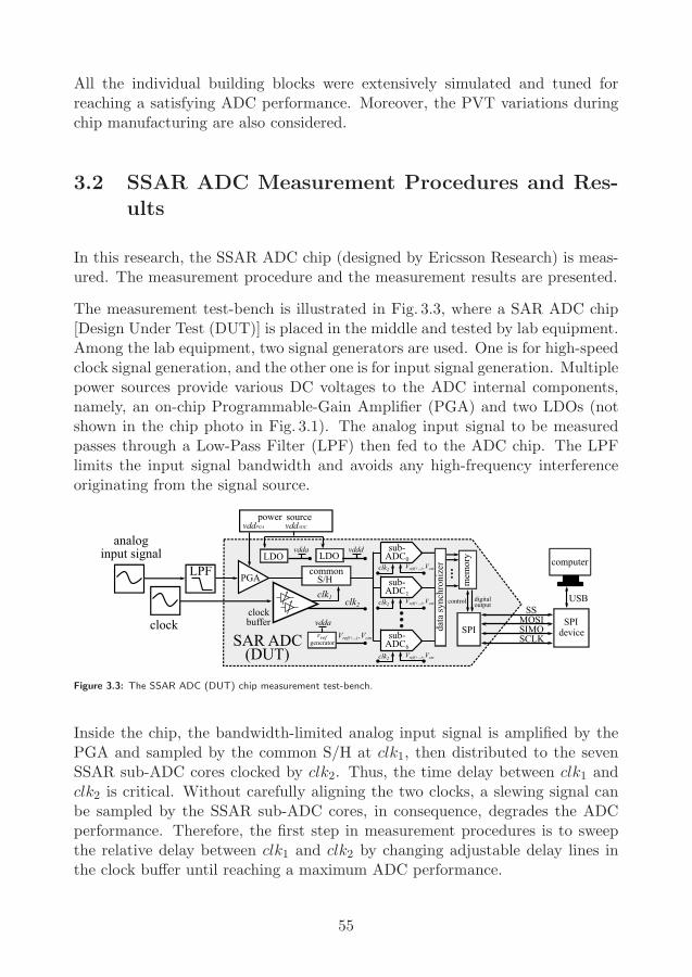
All the individual building blocks were extensively simulated and tuned forreaching a satisfying ADC performance. Moreover, the PVT variations duringchip manufacturing are also considered.
3.2 SSAR ADC Measurement Procedures and Res-ults
In this research, the SSAR ADC chip (designed by Ericsson Research) is meas-ured. The measurement procedure and the measurement results are presented.
The measurement test-bench is illustrated in Fig. 3.3, where a SAR ADC chip[Design Under Test (DUT)] is placed in the middle and tested by lab equipment.Among the lab equipment, two signal generators are used. One is for high-speedclock signal generation, and the other one is for input signal generation. Multiplepower sources provide various DC voltages to the ADC internal components,namely, an on-chip Programmable-Gain Amplifier (PGA) and two LDOs (notshown in the chip photo in Fig. 3.1). The analog input signal to be measuredpasses through a Low-Pass Filter (LPF) then fed to the ADC chip. The LPFlimits the input signal bandwidth and avoids any high-frequency interferenceoriginating from the signal source.
SAR ADC(DUT)
S/HPGA
sub-
data
sync
hron
izer
mem
ory
SPI
control
analogADC0
sub-ADC1
sub-ADC6
LDO LDOvdda vddd
clk1
clock
clk2
clk2
common
sourcepower
digitaloutput
SPIdevice
computer
USB
SCLK
MOSISIMO
SSbufferclock
generator
vddaVref
clk2
clk2
vddPGA
input signal
Vref(+,-) ,Vcm
Vref(+,-) ,Vcm
Vref(+,-) ,Vcm
Vref(+,-) ,VcmLPF
vddADC
Figure 3.3: The SSAR ADC (DUT) chip measurement test-bench.
Inside the chip, the bandwidth-limited analog input signal is amplified by thePGA and sampled by the common S/H at clk1, then distributed to the sevenSSAR sub-ADC cores clocked by clk2. Thus, the time delay between clk1 andclk2 is critical. Without carefully aligning the two clocks, a slewing signal canbe sampled by the SSAR sub-ADC cores, in consequence, degrades the ADCperformance. Therefore, the first step in measurement procedures is to sweepthe relative delay between clk1 and clk2 by changing adjustable delay lines inthe clock buffer until reaching a maximum ADC performance.
55

At the chip output side, a data synchronizer is used to receive and reassembleeach of the ADC digital outputs into a long word length at slow speed and thenstore them in on-chip memory. An external Serial Peripheral Interface (SPI)device communicates with the on-chip SPI module to sequentially read out theADC digital values that have been stored in the on-chip memory. The collec-ted ADC digital output is further post-processed by an appropriate computersoftware, such as MATLAB.
A single SSAR sub-ADC core performance is evaluated by examining its 11output bits, in which one redundant bit is added. The measured ADC outputspectrum, with a 95.7MHz input sine signal sampled at fs=200MHz, is plottedin Fig. 3.4. The resulting maximum SNDR is 48.7 dB, by tuning the on-chipcalibration capacitors and using the aforementioned off-chip DAC imbalanceestimation and calibration methods. Still, third and fifth-order harmonic tonesare visible.
frequency [MHz]0 10 20 30 40 50 60 70 80 90 100
0-10-20-30-40-50-60-70-80-90
-100-110-120
0
[dB] 3H5 H
Figure 3.4: Measured ADC output spectrum of a single sub-ADC core running at fs=200MHz , with 95.7MHz inputfrequency.
Fig. 3.5 (a) shows the SNDR and SFDR of a single SSAR sub-ADC core, withinput signal frequency swept up to 191.4MHz and fs=200MHz. It shows thatthe SNDR is almost constant at approximately 48 dB, and the SFDR is above60 dB.
The seven sub-ADC core output results are combined, post-processed and ana-lyzed, reflecting the 7-channel TI SSAR ADC performance. The measurementresults are shown in Fig. 3.5 (b), where the input signal frequency is swept froma low frequency to Nyquist frequency (735MHz), with an external samplingfrequency for 7-channel TI SSAR ADC of 1.47GHz. Thus, each sub-ADC coreis sampled at 210MHz.
It could be observed that the SNDR and SFDR in the TI SSAR ADC shownin Fig. 3.5 (b) is slightly lower than its single SSAR sub-ADC core performance
56

input frequency [MHz]
7x T
I AD
C S
ND
R, S
FDR
[dB
]
SFDRSNDR
65
60
55
50
45
40
35100 200 300 400 500 600 700
19.1 38.3 57.4 76.6 95.7 114.8 134.0 153.1 172.3 191.4sub-
AD
C c
ore
SND
R, S
FDR
[dB
]
69
60
4845
63
515457
66
(a)
(b)
input frequency [MHz]
SFDRSNDR
Figure 3.5: Measured SNDR and SFDR versus input signal frequency sweep, where (a) shows a single SSAR sub-ADC coreperformance, with fin up to 191.4MHz; (b) shows the 7-channel TI SSAR ADC performance, with fin up toNyquist frequency of 735MHz.
shown in Fig. 3.5 (a) within the same fin range. In a fabricated chip, the sub-ADC cores are not identical, which introduces gain mismatches. It introducesharmonic distortion tones to the ADC output spectrum, which are hard to beentirely removed by the post-processor and result in performance degradation.
Fig. 3.5 (b) also indicates that the SNDR degrades to below 45 dB with an inputfrequency beyond 300MHz, a frequency much lower than the Nyquist frequency.One reason for such a narrow input signal bandwidth is the weak amplifier usedin the common S/H, whose linearity is degraded at a high input frequency. Inthe modified design (TI ASAR ADC), the S/H is driven by a separate supplyvoltage that can be individually optimized. The input bandwidth in S/H canbe further extended by slightly increase its supply voltage.
3.3 SSAR ADC Power Consumption
The simulated and measured SSAR sub-ADC core power consumption is listedin Table 3.1. The second column in the table shows the power consumption fromthe simulation. It includes the average power consumption of global blocks such
57

Table 3.1: Single SSAR sub-ADC core power consumption from the simulation and measurement, and the simulation-adjusted power consumption in the last column.
simulation measurement simulation-adj.component power (uW) % of total power (uW) power (uW)
clock buffer 642 18%3189
798common S/H 845 24% 1050control logic 1006 29% 1250
Vref generator 234 7%543
291comparator 584 17% 725
CDAC 0.002 0% - -
other 184 5% 611 229
total 3495 100% 4343 4343
as the common S/H shared by seven sub-ADC cores, and the power consumptionof SSAR sub-ADC core internal blocks such as clock buffer, SSAR control logic,Vref generator, comparator, CDAC, and other un-categorized blocks. The thirdcolumn shows the percentage of the total sub-ADC core power consumptionregarding each component.
The fourth column shows the measured ADC power consumption. Notice thatthe power consumption of each group of components is combined. These com-ponents operate closely related to each other and can not be fully separated.In other words, it is not possible to directly measure the current and voltageof chip internal components. The power consumption is estimated indirectlyby toggling the SSAR sub-ADC core individual blocks’ enable signals and keeptrack of the differences in current drawn from the external power source. Thedifferences represent how much power is consumed when a set of blocks becomeactive. For example, the clock buffer, the common S/H, and the control logicare all started when enabled, drawing 3189 uW power compared with the casewhen disabled.
The last column, called simulation-adjusted power, is an adjusted power con-sumption by multiplying the total measured power consumption (4343 uW) withthe percentage showing in column three. It reveals an estimation of component-wise power consumption. It can be seen that the common S/H and the SSARcontrol logic occupy almost half of the total power consumption of a sub-ADCcore. The CDAC consumes almost no average power benefitting from the MCSCDAC switching scheme, and it is not feasible to measure such tiny power dif-ferences accurately.
58

3.4 ASAR ADC Simulation Results
In this section, the ASAR ADC simulation results are shown. Specifically, thesub-ADC core post-layout simulations compared to the schematic-level simula-tions are presented. A non-ideality effect introduced by layout is the increasedparasitic capacitance in the capacitor array, which causes the bridge attenuationr deviating from a designed value thus impairs the ADC performance.
Recall that an extra capacitance C ′e=9Cu is required for maintaining a pre-
defined r between the sDAC and the mDAC, as explained in Section 2.5.1. How-ever, due to increased sDAC parasitic capacitance, the C ′
e may not be accurateanymore. The C ′
e can be coarsely tuned on-chip by switching in or out severalunit capacitances. For achieving a maximum SNDR, a post-processor, which iscurrently implemented in the MATLAB, further applies a gain to the sDAC bitweights and swept. An optimized r of sDAC and mDAC bit weights is achievedwhen the SNDR is maximum.
Fig. 3.6 shows the SNDR and SFDR of the schematic-level and post-layout sim-ulation results, with r swept from 0.6 to 1.4. The post-layout simulation resultshows a maximum SNDR of 53.5 dB at r = 0.95. It is slightly smaller thanr = 1 in the schematic-level simulation, at which a maximum SNDR of 53.2 dBis achieved. The unit gain means no adjustment to the sDAC bit weights isrequired in the post-processing.
r [V/V]
[dB]
0.6 0.7 0.8 0.9 1.0 1.1 1.2 1.3 1.440
45
50
55
60
65
70
SNDRSFDR
schematicSNDRSFDR
post-layout
Figure 3.6: Single ASAR sub-ADC core post-layout vs. schematic-level simulations, with gain swept between sDAC andmDAC bit weights, for a maximum SNDR.
The ADC output spectra from the previous simulations are plotted in Fig. 3.7,with an optimized r applied in the post-processor. Note that the two spectraare similar in terms of their noise floor and signal peak but differ in the DC bin.The ADC post-layout output spectrum shows a higher DC offset than from theschematic-level simulation. Such DC offset is usually not included in the SNDR
59

calculation, resulting in similar SDNRs from the two simulations.
frequency [MHz]0 10 20 30 40 50 60 70 80 90 100
-100
-60
-40
-20
0
[dB]
-80
schematicpost-layout
Figure 3.7: ADC output spectra for schematic and post-layout simulation results at the maximum SNDR.
Before sending the chip for fabrication, the post-layout simulation of the fullchip design is usually performed, providing the designer an opportunity to es-timate the fabricated chip’s performance and paving the way to success. How-ever, it is not possible without extensive simulation time and computing re-sources, especially in large designs. In this work, the complete 10-bit 7-channelTI ASAR ADC design is simulated at schematic-level in five process corners,with thermal noise enabled in the simulator, and these simulation results areplotted in Fig. 3.8. The process corner models are described by two letters, re-ferring to the corner model of NMOS transistors and PMOS transistors. Forexample, tt means typical PMOS transistors and typical NMOS transistors,which is a normal operational condition; ss means all the NMOS and the PMOStransistors are slow, and ff means all the NMOS and the PMOS transistors arefast.
corner
50
60
70
[dB]
ff fs sf ss tt
SNDRSFDR
Figure 3.8: SNDR and SFDR of the 10-bit 7-channel TI ASAR ADC, simulated in five process corners.
In all these simulations, the input amplitude is full-scale voltage, and the inputfrequency is 211MHz. The TI ASAR ADC is sampled at 2GHz, and the tunableparameters are carefully selected, i.e., the clock delay between the commonS/H and the sub-ADC cores is properly chosen, and the pulse width of thecomparator clock generated from ACL is optimized. It can be seen in Fig. 3.8,
60

Table 3.2: Simulated power consumption in 10-bit ASAR and SSAR sub-ADC cores.
10-bit ASAR ADC 10-bit SSAR ADCpower (uW) power (uW)
fs 300MHz 390MHz 500MHz 300MHz 390MHz
comparator 897 1010 1078 877 974
digital 945 1181 1352 915 1143
-unit cells 536 664 751 609 763
-clock gen. 410 517 601 - -
-ring count. - - - 306 380
clock buffer 78 96 117 606 780
total 1920 2287 2547 2398 2897
that the SNDR is approximately 50 dB in all the corners, and the SFDR isapproximately 60 dB.
The SNDR of TI ASAR ADC (shown in Fig. 3.8) is lower than the single ASARsub-ADC core (shown in Fig. 3.6). Further analysis reveals that the degradedperformance is caused by increased thermal noise in the global blocks such asthe common S/H and the input buffer. These two blocks will be optimized infuture designs.
3.5 ASAR ADC Power Consumption
Since the ASAR and SSAR sub-ADC core has similar building blocks and ar-chitectures, their key component power consumptions are very similar whenrunning at the same fs. Table 3.2 lists the power consumption breakdown ofmain components in the 10-bit ASAR and SSAR sub-ADC core, sampled atfs of 300MHz and 390MHz. Besides, the ASAR sub-ADC core is sampled atan additional sampling frequency fs=500MHz, and its power consumption isincluded as well. However, this frequency becomes too high for the SSAR ADCto function correctly.
As seen from Table 3.2, the clock buffer in the SSAR sub-ADC core consumesalmost eight times higher power than the same clock buffer in the ASAR sub-ADC core. It is because a multi-GHz external clock needs to be buffered in theSSAR sub-ADC core, while a low duty cycle external sampling signal with afrequency in hundreds of MHz is buffered in the ASAR sub-ADC core.
61
3.6 Conclusion
In this chapter, the SAR ADC chip implementation, simulation, and meas-urement results are shown. Both the SSAR and ASAR ADC have 7-channeltime-interleaved architecture and were implemented in 22 nm FD-SOI CMOS.
A single SSAR sub-ADC core was measured, showing an SNDR of 48 dB withan input frequency up to the sampling frequency of 200MHz. Seven identicalSSAR sub-ADC cores are time-interleaved to a 7-channel TI SSAR ADC, con-suming a total power of 30.1mW. This total power includes the seven SSAR sub-ADC cores, their surrounding biasing blocks, and a common S/H. On average,each sub-ADC core, together with the necessary surrounding blocks, consumes4.3mW power and results in a FoMs of 152 dB.
The ASAR ADC was simulated using the circuit simulator Spectre in Cadence(www.cadence.com), and the results are analyzed. The post-processor imple-mented in MATLAB allows a maximum ADC performance to be achieved byadjusting the bridge attenuation r of sDAC and mDAC in fine steps. The ASARsub-ADC core is simulated both in schematic-level and post-layout, resulting inan SNDR of 53.2 dB, and 53.5 dB respectively. In a higher hierarchy level, the7-channel TI ASAR ADC was simulated across five process corners, resultingin an SNDR of approximately 50 dB. Compared with a single ASAR sub-ADCcore, the 7-channel TI ASAR ADC exhibits a decreased performance, partiallydue to thermal noise introduced by the input buffer and the common S/H.
Regarding the circuit design, the control logic in the SSAR ADC is based onpure-digital standard-cell architecture, which scales well with the future sub-micrometer CMOS technology node. However, the SSAR ADC is less power-efficient since the control logic and the comparator are clocked by a high-speedexternal clock signal, which needs to be adequately buffered by a power-hungryclock buffer in a practical ADC chip design. In this particular design, such aclock buffer consumes approximately 25% of the total power.
It shows that an ASAR ADC is more power-efficient than a similar SSAR ADC.The ASAR ADC is clocked by an external sampling signal with short pulse-widths and a much-reduced frequency, compared with the high-speed externalclock in the SSAR ADC. These sampling pulses synchronize the start of eachsample conversion and trigger the sampling of the analog input signal. Thesimulation results show that a clock buffer in the ASAR ADC consumes up toeight times less power than an identical clock buffer in the SSAR ADC.
62

Chapter 4
High-Speed ΔΣ ADC
4.1 Introduction
The ΔΣ ADC is categorized as an oversampled ADC, which incorporates DSMto convert an analog input signal to a fast varying digital representation. Forachieving a similar input bandwidth compared with the Nyquist-rate ADC,the ΔΣ ADC typically uses a significantly higher sampling rate. An importantterm: OSR defines the ratio between the Nyquist rate and the signal bandwidth.The ΔΣ ADC has the potential to achieve a high resolution by sampling thecomparator at a very high rate to distribute the noise power injected into thesampled signal to a wider bandwidth, resulting in an in-band noise becomes afraction of the total noise.
A simple DSM may only incorporate one bit to represent the analog signal butcan still reach an ADC resolution up to 16-bit. The single-bit DSM was studieddate back to 1996 by Aziz et al. [50]. The single-bit DSM is intrinsic linearsince the quantizer in DSM can be designed merely using a 2-level comparator.The feedback circuit is also linear since the multi-bit DAC is avoided. Thefeedback DAC output is either a plus or a minus reference voltage, which willnot deteriorate the overall system resolution. One drawback of the single bitarchitecture is that it usually necessitates much higher OSR than the multi-bitequivalent for achieving a similar SQNR.
The DSM usually incorporates an LF, which provides some noise filtering tofurther reduce in-band noise. The LF can be constructed by a chain of integ-rators, whose number determines the order of LF. Its purpose is to suppress thein-band noise but leave the signal unchanged. It “pushes” the in-band noise to
63

high frequencies, effectively increases in-band ADC resolution.
The signal injected into the LF is the difference between the input and thequantized output. By using a multi-bit quantizer and DAC, the input voltagesto integrators are reduced. The linearity of the feedback DAC affects the DSMaccuracy as the non-linearities of the outer-most DAC can be modeled as anadditional input to the ADC without being shaped by the LF. Therefore, es-timation and calibration methods are important to improve the DAC linearityand the ADC resolution.
Above all, a high-performance DSM usually incorporates a high-order multi-bitarchitecture. A high-order DSM efficiently shapes the quantization noise, whichshows a higher suppression on the in-band noise and a higher amplification onthe out-of-band noise. However, high-order DSM may also experience stabilityissues.
Furthermore, Continuous-Time (CT) DSM architecture is implemented in thehigh-speed design. The CT DSM generally benefits from two aspects comparedwith its Discrete-Time (DT) counterpart. First, CT DSM has an inherent anti-aliasing function. It does not require a dedicated anti-aliasing filter that isusually required in a discrete-time DSM. Second, the CT DSM is, in general,faster than the DT DSM. The components in the LF are continuous-time in-tegrators such as a gm-C integrator or an active-RC integrator, whose designdetails will be explained in the following sections.
For achieving a large input bandwidth, the CT DSM could be sampled at ahigh sampling rate. A ΔΣ ADC design previously presented by Bolatkale etal. in [26] presented that as large as 125MHz input bandwidth can be achievedwhen sampled at 4GHz. For reaching such a large input bandwidth, inevitably,the OSR becomes low compared with conventional DSMs, which incorporates alarge OSR, requiring aggressive noise shaping.
In this chapter, a high-speed ΔΣ ADC design is proposed. The target applic-ations are in high-performance communication systems, such as base stationdevices. The following sections focus on a high-speed single-loop ΔΣ ADCdesign, study the ADC operation principles and present component-level imple-mentations.
The behavior model construction will be presented in Section 4.2.1. Various ΔΣADC architectures will be explained, and the synthesize of DT DSM coefficientswill be addressed. Then, in Section 4.3, the synthesized DT DSM model istransformed into a CT DSM equivalent, with a set of CT coefficients calculatedusing time-invariant transformation from the DT coefficients. The Excess Loop
64

Delay (ELD) will be addressed, which is an important consideration during thetransformation of the coefficients from DT to CT. Furthermore, an additionalfast feedback path is added. A new set of coefficients are calculated so that anELD larger than one clock cycle between the quantizer and feedback DACs canbe compensated.
In the last section, the CT DSM model will be mapped into a component-level design. The ΔΣ ADC design, implemented in 28 nm FD-SOI CMOS, willbe explained. The ADC is sampled at a target sampling frequency of 5GHz,achieves a maximum signal bandwidth of 250MHz. The component-level designincorporates inverter-based integrators in its loop filter and CML in the digitalblocks to increase the digital signal speed.
4.2 Model Construction in MATLAB
4.2.1 ΔΣ ADC Model
The first step in constructing a ΔΣ ADC is selecting an appropriate discrete-time architecture. Four types of basic architectures can be chosen for a high-order modulator, as discussed extensively in [11]. There are two feedback archi-tectures: Cascade of Integrators with Distributed Feedback (CIFB) and Cascadeof Resonators with Feedback (CRFB). Each has an LF containing a cascade ofN delaying or delaying-free integrators (where N is the order of the LF). Simil-arly, two feed-forward architectures contain the chain of integrators: Cascade ofIntegrators with Feed-Forward Summation (CIFF) and Cascade of Resonatorswith Feed-Forward Summation (CRFF). Each has a summation node that sumsand amplifies the feed-forward signals from the integrator outputs and the inputsignal.
The aforementioned four ΔΣ ADC architectures have been illustrated in Fig. 4.1,with a 4th order LF shown for illustration purposes. Fig. 4.1(a) illustrates theCIFB and CRFB architectures, and Fig. 4.1(b) illustrates the CIFF and CRFFarchitectures.
The quantizer is a 4-bit flash ADC, with 24−1 comparators converting the analogsignal to digital codes at a fast pace, then drive the feedback DACs. For thecomponent matching perspective, the feedback DAC is implemented with unitcell design, which means identical DAC unit cells are used several times. Again,any mismatch in the outer-most DAC will inject into the system in parallel withthe input. These mismatches result in distortions, which requires a calibration
65
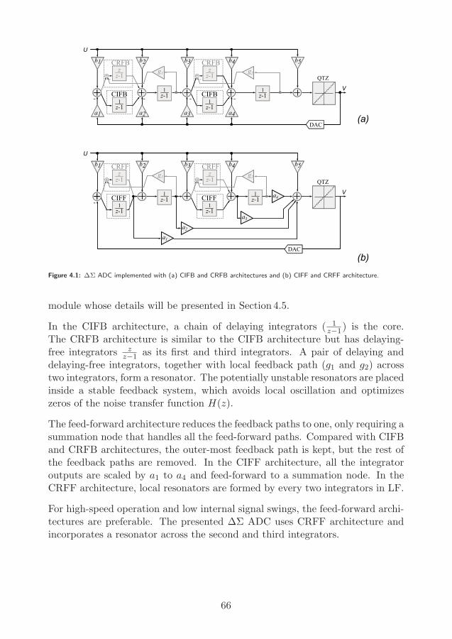
U
QTZ
DAC
V
U
QTZ
DAC
V
(a)
(b)
b1 b2
z-11
b3
z-11
b4
a4a3a2a1
z-11
b5
CIFB- - - -z-11
CIFB
b1 b2
z-11
b3
z-11
b4
z-11
b5
CIFF
z-1z
CRFF
-z-11
CIFF
-
a1
a2
a3
a4
g1 z-1z
CRFF
-
z-1z
CRFB
- z-1z
CRFB
-
g2
g1 g2
Figure 4.1: ΔΣ ADC implemented with (a) CIFB and CRFB architectures and (b) CIFF and CRFF architecture.
module whose details will be presented in Section 4.5.
In the CIFB architecture, a chain of delaying integrators ( 1z−1) is the core.
The CRFB architecture is similar to the CIFB architecture but has delaying-free integrators z
z−1 as its first and third integrators. A pair of delaying anddelaying-free integrators, together with local feedback path (g1 and g2) acrosstwo integrators, form a resonator. The potentially unstable resonators are placedinside a stable feedback system, which avoids local oscillation and optimizeszeros of the noise transfer function H(z).
The feed-forward architecture reduces the feedback paths to one, only requiring asummation node that handles all the feed-forward paths. Compared with CIFBand CRFB architectures, the outer-most feedback path is kept, but the rest ofthe feedback paths are removed. In the CIFF architecture, all the integratoroutputs are scaled by a1 to a4 and feed-forward to a summation node. In theCRFF architecture, local resonators are formed by every two integrators in LF.
For high-speed operation and low internal signal swings, the feed-forward archi-tectures are preferable. The presented ΔΣ ADC uses CRFF architecture andincorporates a resonator across the second and third integrators.
66

4.2.2 DT Coefficients
Amethod of synthesizing a DT architecture can be performed in MATLAB usingthe Delta-Sigma toolbox [51]. It is a tool for synthesizing the DT coefficientsa, b, and g and an NTF from given parameters such as LF order, Out-of-Band Gain (OBG), OSR, and whether the NTF zeros are optimized. Thereare trade-offs between these parameters: a higher-order LF provides aggressivenoise shaping, requiring a long chain of integrators which increases delay andharms loop stability; a higher OSR results in a lower in-band noise, but inneed of a proportionally higher sampling frequency; the OBG determines themaximum out-of-band gain for noise shaping, but still, a too high OBG maylead to stability issues.
The low OSR ΔΣ ADC requires an aggressive noise shaping to reach a certainADC resolution. The chosen parameters are 4th order, OSR of 10, OBG of3.5, and optimized for at least one zero at band-center. The pole-zero plot isgraphically illustrated in Fig. 4.2, where the zeros are separated due to zerooptimization, and poles are within the unit-circle. The NTF is:
NTF=(z − 1)2(z2 − 1.93z + 1)
(z2 − 0.7923z + 0.176)(z2 − 0.8354z + 0.4464)(4.1)
-1 -0.5 0 0.5 1-1
-0.5
0
0.5
1
Re(Z)
Im(Z)
Figure 4.2: Pole and zero plot of an NTF with parameters: 4th order LF, OSR=10, and OBG=3.5.
This NTF is mapped into the DT CRFF architecture, where a set of DT coef-ficients is generated. During the mapping from the transfer function to realimplementation, a high-resolution internal quantizer will potentially result in ahigh-accuracy ADC since each 1-bit increase in resolution results in a 6 dB ac-curacy improvement. A drawback of the multi-bit DAC is their linearity issues,which require sufficient linearity in the component design in components.
A DT CRFF DSM is constructed in the Simulink model in MATLAB usingthe synthesized coefficients. The simulation results of the Simulink model and
67

the calculations from a mathematical model show marginal differences. In thenext section, DT to CT transformation will be explained. The CT architectureis transformed from a DT equivalent, but with considerations of ELD. Thecalculations of ELD compensation will be covered in Section 4.3.3.
4.3 DT to CT Transformation
4.3.1 Impulse-Invariant Transformation
Conventionally, the architecture is synthesized in DT. It means that a S/Hcircuit is placed before the circuit to provide sampled input to the loop filter.The internal components are discrete-time circuits, such as switched capacitorintegrator. One step further, CT architecture is another alternative. It has aninherent anti-aliasing feature and handles the continuous varying signal. As aresult, circuit speed is improved since the slow-slewing switch-capacitor circuitsare avoided.
Prior researches addressed constructing an equivalent CT model transformedfrom a DT counterpart, such as [52] and [53]. Moreover, in [54], an intuitiveway of calculating equivalent CT coefficients from DT was proposed.
The CT model is transformed from an equivalent DT model to be used in thehigh-speed ΔΣ ADC. It has been implemented at component-level and fab-ricated in a chip. The DT to CT conversion is calculated based on impulse-invariant transformation. At the quantizer sampling instant, the impulse re-sponse seen at the quantizer input is identical between CT and DT models.
In the CT model, feedback DAC pulse shapes determine the integration valueswithin one clock period. AppendixA presents the detailed calculations of DTto CT transformation. In short, the goal is to match the LF output voltagesin CT DSM with the DT DSM at the sampling instant, when a DAC pulsefeedback either a Return-to-Zero (RZ) or a Non-Return-to-Zero (NRZ) pulse tothe Linear Time-Invariant (LTI) system. Thus, in the feedback loop, the signalsettles within one clock cycle, and the transformed CT architecture behavesidentically to the DT counterpart.
Besides, when the NTF zeros are optimized, the original DT model has reson-ators across the first two and the last two integrators. It is also possible to formthe resonator across the middle two integrators to reduce the load to the lastintegrator by re-calculating the coefficients.
68

4.3.2 DAC Output Pulse Shape
In the DT to CT transformation, the DAC feedback pulse shape is anotherconsideration. NRZ DAC feedback pulses are commonly used, but its perform-ance is limited by the inter-symbol-interference (ISI) from the switching events.Another alternative is to use RZ DAC feedback pulses, which benefits from re-ducing ISI commonly seen from an NRZ DAC. However, using RZ pulse willincrease clock jitter sensitivity [55], although the unequal DAC edge rise andfall times are avoided by implementing differential architecture [56].
The NRZ and RZ DAC feedback pulses are illustrated in Fig. 4.3. The paramet-ers α and β represent the start and stop time of the DAC pulse, respectively,related to T . For example, in an NRZ feedback pulse, α=0 and β=1 whenELD=0 and α=0.5 and β=1.5 when ELD=0.5T .
0 T
VDAC
time
T/2 3T/2
0 T
VDAC
timeT/2 3T/2
(a)
(b)
TT
TT
Figure 4.3: The DAC output pulses vs. T , where (a) shows an NRZ DAC and (b) shows an RZ DAC pulse.
4.3.3 ELD Compensation
The ELD measures the time difference between the quantizer output instant andthe next LF output becoming available, which is an important consideration incalculating coefficients in the CT DSM. Usually, an ELD should not be largerthan one clock cycle for correct transformation between DT to CT model. How-ever, under a high clocking rate, the feedback signal may not settle in time. Insuch a scenario, the longest ELD from the sampling instant to the next analogvoltage appearing at the quantizer input can be larger than one clock cycle.
The larger than one clock cycle ELD is partially due to the relatively slow quant-
69

izer. The propagation delay from the sampling instant to a settled feedbackDAC output could be large. In the previous work presented by Balagopal andSaxena, a 1.5 T ELD can be successfully compensated by creating a fast-looparound the last integrator using a sample-and-hold [57]. Without this additionalfast feedback loop, the DT to CT transformation becomes incorrect due to anunmatched sample in the CT impulse response.
The ELD compensation is studied by examining the proposed high-speed ΔΣADC architecture in Fig. 4.4. It is based on the CRFF architecture, where twoadditional feedback paths afb and adly are introduced for ELD compensation.Based on the calculations in SectionA.2.2 in AppendixA, it is clear that adifferent direct feedback path is required for the CT transfer function matchingto the original DT counterpart.
Instead of adding an analog fast-feedback path around the last integrator, in thepresented ΔΣ ADC, a fast DAC is scaled by afb, to directly inject the quantizedsignal back to the summation node. This DAC is not clocked, which outputsan analog voltage immediately when the quantizer completes a conversion. Theother DACs are delayed by T , where a typical value 0.5T is not sufficient.
V(n)
U(t)+
+
+
+
-
- QTZ
4b
DAC
DACELD1
ELD2
ELD3
ELD4
active summation
SfS c2 S
fSSfS
SfSc3 c4 a4
a3
a2
a1
Z-1adly-c1
afb-g
b
Figure 4.4: Proposed DSM architecture in the Simulink model, with ELD paths shown.
The detailed calculations of DT to CT transformation are presented in the Ap-pendixA, which is based on time-invariant transformation. In Table. 4.1, theconverted CT coefficients are listed, and the original DT coefficients are presen-ted. The estimated ELD values are based on each component delay simulatedat the component-level. In total, four ELD paths need to be considered, whereeach ELD path is marked with a number. The longest ELD is ELD1, which hasa nominal value of 1.6T estimated from the simulation.
70

Table 4.1: The DT model coefficients from a 4th order LF, 4-bit quantizer and DAC, OSR=10 CRFF architecture, andits equivalent CT model coefficients.
coefficient DT architecture CT architecture
a1 0.9214 2.2162
a2 1.3808 3.3136
a3 0.6513 3.9187
a4 0.2345 4.4927
adly - 1.6885
afb - 2.3022
b 1 2
c1 1 2
c2 1 0.4
c3 1 0.3
c4 1 0.3
g 0.0701 0.2336
4.3.4 Dynamic Range Scaling
The CT coefficients calculated in AppendixA using Eq.A.15 and Eq.A.16 aredynamic range scaled to limit the LF internal nodes signal swings. In Table4.1, the equivalent CT coefficients are scaled by applying coefficients c. Theoutput nodes voltages are simulated under different input signal frequencies toguarantee no over-ranging problem occurs. The scaled CT coefficients are thenimplemented at component-level, which will be explained in the next section.
4.4 Component-Level Implementation
The synthesized model is further realized at the component-level. A ΔΣ ADCwas designed in 28 nm FD-SOI CMOS and fabricated. The ADC input band-width is up to 250MHz, sampled at 5GHz. The output is first stored in thememory and then read out sequentially at a slower pace for further signal pro-cessing.
Designing the high-speed ΔΣ ADC becomes challenging, which requires select-ing high-performance components and laying out the circuit carefully. Espe-cially in feed-forward architecture, a high-speed summation node needs to bedesigned. From the simulation, the designed ΔΣ ADC achieves approximately80 dB SNDR in 250MHz signal bandwidth.
71

4.4.1 LF Design
A complete component-level LF design is shown in Fig. 4.5. The LF is builtwith a chain of integrators, where the first integrator is an active-RC integrator,and the rest are gm-C integrators. Each of the feedback current-steering DACsgenerates a current proportional to a 15-bit thermometer code from the quant-izer. Note that the DAC1 and the DACdly are clocked by a high-speed externalclock clk. It is also the sampling signal to the quantizer. Equivalently, one clockcycle delay is added in the feedback loop.
Up
Um
Vp
Vm
TpTn
gm2+
-gm3+
-
-
+
+
-gm4+
- -
+
+--+
+--+
+--+
+- -+
+-+-
gmg+
-
-
+
DAC1
DACfb
DACdlyclk clk
+- +-
+-amp C2 C3 C4
C1p
C1mR1p
R1m RS
s1
s2
s3
s4
Active Summation
cal4 x15
15-bit thermometer code from QTZ
ImII
IpII
Figure 4.5: LF component-level design, including integrators, an active summation block, and feedback DACs.
4.4.1.1 Integrator Design
Inside the LF shown in Fig. 4.5, active-RC and gm-C integrators are used. Thefirst integrator is an active-RC integrator, which has better linearity and canhandle a large input and output signal swing. The amplifier schematic is shownin Fig. 4.6(a), which is based on a single-stage integrator with a local cross-coupled negative load connected to the drains of the NMOS transistor inputpair (N1 and N2). A large Gain-Bandwidth Product (GBW) is needed for high-speed applications, therefore, it was designed with a DC gain of 53 dB and aGBW of 7.8GHz. The common-mode voltage of outputs Vp and Vm is detectedusing two resistors R1 and R2.
The following integrators are built based on well-known CMOS inverters [58],which uses inverters as transconductor (gm1, gm2 and gm3) and uses capacitiveload for integration. Instead of being used in pure digital circuits, the invertersare biased at a common-mode voltage (Vcm) for extended usage in an analogway.
Inverter-based integrator schematic is shown in Fig. 4.6(b). In total, six inverters
72
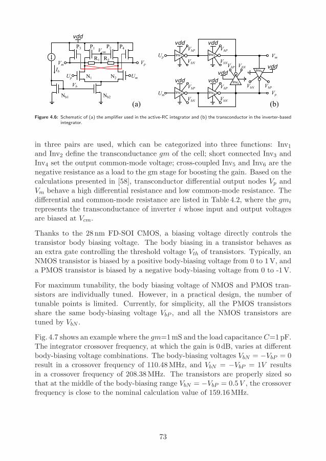
Vb
Up Um
Vm Vp
vdd
R2
P1 P2
N1 N2
Nb2Nb1
Vcm
Ib
P3 P4Inv1
VbN
Inv2 Inv4
Inv3
Inv5
Inv6
(a) (b)
R1
Um
Up
Vp
VmVbP
vdd vdd
vddvdd
vdd
vddVbN
VbP
VbN
VbP
VbN
VbP
VbP VbN
VbPVbN
Figure 4.6: Schematic of (a) the amplifier used in the active-RC integrator and (b) the transconductor in the inverter-basedintegrator.
in three pairs are used, which can be categorized into three functions: Inv1and Inv2 define the transconductance gm of the cell; short connected Inv3 andInv4 set the output common-mode voltage; cross-coupled Inv5 and Inv6 are thenegative resistance as a load to the gm stage for boosting the gain. Based on thecalculations presented in [58], transconductor differential output nodes Vp andVm behave a high differential resistance and low common-mode resistance. Thedifferential and common-mode resistance are listed in Table 4.2, where the gmi
represents the transconductance of inverter i whose input and output voltagesare biased at Vcm.
Thanks to the 28 nm FD-SOI CMOS, a biasing voltage directly controls thetransistor body biasing voltage. The body biasing in a transistor behaves asan extra gate controlling the threshold voltage Vth of transistors. Typically, anNMOS transistor is biased by a positive body-biasing voltage from 0 to 1V, anda PMOS transistor is biased by a negative body-biasing voltage from 0 to -1V.
For maximum tunability, the body biasing voltage of NMOS and PMOS tran-sistors are individually tuned. However, in a practical design, the number oftunable points is limited. Currently, for simplicity, all the PMOS transistorsshare the same body-biasing voltage VbP , and all the NMOS transistors aretuned by VbN .
Fig. 4.7 shows an example where the gm=1mS and the load capacitance C=1pF.The integrator crossover frequency, at which the gain is 0 dB, varies at differentbody-biasing voltage combinations. The body-biasing voltages VbN = −VbP = 0result in a crossover frequency of 110.48MHz, and VbN = −VbP = 1V resultsin a crossover frequency of 208.38MHz. The transistors are properly sized sothat at the middle of the body-biasing range VbN = −VbP = 0.5V , the crossoverfrequency is close to the nominal calculation value of 159.16MHz.
73
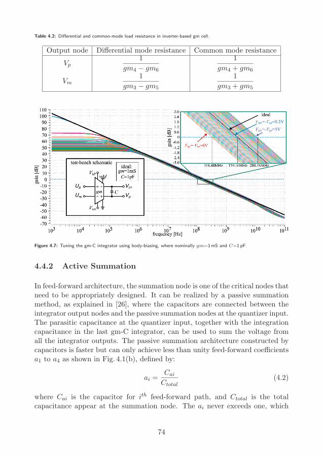
Table 4.2: Differential and common-mode load resistance in inverter-based gm cell.
Output node Differential mode resistance Common mode resistance
Vp1
gm4 − gm6
1
gm4 + gm6
Vm1
gm3 − gm5
1
gm3 + gm5
Figure 4.7: Tuning the gm-C integrator using body-biasing, where nominally gm=1mS and C=1pF.
4.4.2 Active Summation
In feed-forward architecture, the summation node is one of the critical nodes thatneed to be appropriately designed. It can be realized by a passive summationmethod, as explained in [26], where the capacitors are connected between theintegrator output nodes and the passive summation nodes at the quantizer input.The parasitic capacitance at the quantizer input, together with the integrationcapacitance in the last gm-C integrator, can be used to sum the voltage fromall the integrator outputs. The passive summation architecture constructed bycapacitors is faster but can only achieve less than unity feed-forward coefficientsa1 to a4 as shown in Fig. 4.1(b), defined by:
ai =Cai
Ctotal(4.2)
where Cai is the capacitor for ith feed-forward path, and Ctotal is the totalcapacitance appear at the summation node. The ai never exceeds one, which
74

results in a signal attenuation after the summation.
Another alternative is using active summation, which uses an active summingamplifier in the LF to sum feed-forward voltages. A gain of one or larger canbe realized using the active summation, requiring a high-bandwidth amplifierto accomplish it. This is attractive since it could amplify rather than attenuatethe feed-forward signals.
Revisit the coefficients shown in Table 4.1, in which the feed-forward pathsrequire coefficients larger than one. These large coefficients are partially due tothe limited input and output swing in the integrators. The active summationblock implemented in this work is based on gm-R architecture, as shown inFig. 4.5. The cores in s1 to s4 are the inverter-based transconductors, similar tothose used in the aforementioned integrators.
4.4.3 Quantizer Design
The quantizer is the main decision block in a ΔΣ ADC. The quantizer has aspeed requirement since any delay introduced will directly influence the feedbackloop delays. A large delay impairs the loop stability if it is beyond the coefficientstuning range.
Flash ADC is fast to convert an analog input signal to a digital output. Thearchitecture of a Flash-based quantizer is similar to Fig. 1.5 (a).
The Flash quantizer output is a thermometer code, similar to a thermometermeasuring temperature: a bar rises with increased temperature and falls at adecreased temperature. The digital representation of an analog input voltage isthe number of logic ones of the low-weight bits counting from b0. For example,in a 4-bit quantizer, all zeros in the 15 output bits represent an ADC digitaloutput of 0, and all ones mean a digital output of 15, in decimal representation.The thermometer code is then encoded into binary code by an encoder builtwith readily available digital standard cells.
4.4.4 Current-Steering Feedback DACs
The feedback DAC is a crucial component that converts the quantized digitaloutputs back to the analog domain. In the feedback system, negative coefficientsare accomplished by subtracting the DAC analog outputs from the desired sig-nals, either current or voltage.
75

In high-speed operations, current-steering DAC is preferable. The digital codesare converted to an analog current proportional to the digital value, and suchfeedback current is injected into a selected node in the LF integrator chains.
All the DACs have similar architectures, where each DAC consists of multipleunit cells, and their output currents are superpositioned at the DAC outputnode, becoming the DAC output current. In the specific architecture presentedin this research, the outer-most DAC (DAC1 in Fig. 4.5) is connected to thevirtual ground nodes Ip and Im of the amplifier in the first active-RC integrator.The DAC differential current is subtracted from the differential input current,which is the current flowing through the input resistors R1p and R1m whenan input signal is applied. The schematic of the outer-most DAC is shown inFig. 4.8, which incorporates a 4-bit tuning functionality to each of their internalunit cell for improved linearity.
CML DFF
1.8V
-0.8V
cal<3>
8Ical
4-bit tuningin outer-most
DAC
Vm
Vpvdd vdd vdd
clkDp Dm
QTZ
clk
Vp(i) IpIm
N1 N2
P1 P2
VcasP
VbiasP
VcasN
VbiasN
Pcas
Pb
Ncas
Nb
vdd
Nt2 Nt1
cal<2> cal<1> cal<0>
4Ical
2Ical
IcalIcal
15
15
1515
DAC unit cell
15x
Vm(i)
ImIp
Figure 4.8: Outer-most DAC architecture with 4-bit biasing current tuning.
Note that the supply voltage to the DAC unit cells is much higher than thestandard 1V supply voltage. The technique is similar to [26], where the highsupply voltage is 1.8V, and the low supply voltage is -0.8V to provide enoughheadroom for the current source devices to reduce DAC noise [59]. There arecascode transistors Pcas and Ncas to the current source transistors Pb and Nb,respectively, which improve the biasing current accuracy and reduce the voltageappears on top of the middle four switching transistors. The current sourcetransistors Pb and Nb are thick oxide gate devices to operate at high voltage.
The DACdly and DAC1 are clocked at the same clock edge as the quantizer,equivalent to creating one clock cycle delay between the quantizer and DACs.The DACfb, is the one directly controlled by the quantizer, i.e., whenever a com-
76

parison is completed, the DAC immediately process the digital output withoutwaiting for a clocking pulse. From Fig. 4.5, it can be seen that the latter twoDACs inject currents onto the summation resistor Rs. In such a way, the DACcurrents are subtracted from the current from the active summation block. Thenet current is applied to the summation resistor Rs and becomes LF outputvoltage ready to be compared by the quantizer.
4.4.5 CML in Quantizer and DAC
The CML circuit is beneficial in high-speed digital circuit designs. In the presen-ted work, the CML circuits have been extensively used in the quantizer andthe DAC. Compared with a typical CMOS digital logic that incorporates sev-eral NMOS transistors and PMOS transistors, the CML circuits mainly useNMOS transistors with constant bias current. The CML inverters are betterthan CMOS inverters since it can operate with higher operating frequency atlower supply voltage. It has been studied in [60] based on model simulationresults and experiments.
A CML inverter and a CML buffer schematic are shown in Fig. 4.9 (a), whereonly the NMOS transistor is used as current switching components. The connec-tion between output nodes (Vp and Vm) and drains of input transistors (N2 andN1) determines whether the circuit is an inverter or a buffer (shown in gray).The PMOS transistor, which is typically used in the conventional CMOS invert-ers, are replaced with resistors. The constant bias current flowing in the CMLinverter is determined by the tail current source transistor N3, and the outputcommon-mode voltage is determined by this current and the load resistors R1
and R2, with a nominal value of 750mV under 1V supply voltage vdd.
Fig. 4.9 (b) shows the CML latch schematic. There is a pair of current switchingtransistors N5 and N6 clocked by clk, switching the CML latch between theinput tracking mode and the latching mode. In the input tracking mode, thecircuit is similar to a CML buffer, and the differential outputs Vp and Vm trackthe differential input value Vp and Vm. Next, the latch mode is activated whenthe clk is high. The Vp and Vm will hold for a duration until the clk becomes lowagain, which controls the current flowing to one of the cross-coupled transistorsN3 and N4. Furthermore, a small PMOS transistor (Prst) is used to facilitatethe reset of the value stored in the CML latch, which conducts during the inputtracking mode when the clk is low.
77

(a ) (b )
UmUp
VmVpR1 R2
vdd
Vb constantbias currentN3
N1 N2
vdd
R1 R2
UmUp N1 N2
N5
clk
VbN7
N6
clk
N4N3
Vm
Vp Prstclk
constantbias current
Vp(buffer)Vm(buffer)
Figure 4.9: Schematic of (a) a CML inverter or a CML buffer, and (b) a CML latch with a PMOS transistor reset switch.
4.5 DAC Unit Cell Mismatches and Tuning
Due to the design complexity and the PVT variations, extensive tunings arerequired for an optimized DSM performance. There are two main types oftuning methods used in this work: 1) analog bias voltage and current tuning,and 2) digital calibration.
4.5.1 Bias Voltage and Current Tuning
The analog tuning of part of the design was already addressed in the previoussections. For example, the integrators are tuned by altering their body-biasingvoltages, which have dedicated pins on the chip connected to different voltagesources externally. Based on the simulation, altering the transistor body-biasingvoltages lead to changes to the integrator crossover frequency, resulting in atuning range of approximately ±30%.
The bias current of the CML cells is tuned for reaching a desirable common-mode output voltage to compensate for the resistance variations. Therefore, thecurrent sources in the CML cells can be tuned in a small range to compensatefor resistance variation.
Furthermore, bias currents to the feedback DACs are individually tuned. Thesimulations show that the required output current from the DACdly is sensitiveto the ELD variations, which needs a tuning range of approximately ±30%.
78

4.5.2 Digital Tuning
switchlogic
QTZ
clk
15 15
15xIm
Ip
DAC unit cell
DAC unit cell(extra)
Dm+Tm
Dp+Tp
Dp Dm
Tp
Tm
DAC unit cell(reference)
Tp
Tm
+-
+-
+-
+-
+-
+-
Figure 4.10: DAC conceptual architecture, including 15 DAC unit cells, an extra unit cell, and a reference unit cell.
In addition to the analog tuning, digital tuning is implemented in the outer-mostDAC for further DAC linearity adjustments. An extra unit and a reference DACunit cell are integrated into the outer-most DAC for injecting the test sequence,as shown in 4.10. The reference cell is controlled by a pair of test bits Tp andTm, while the switching logic recombines the input code to each DAC unit cell.The test bits are routed to one of the DAC unit cells at a time, and the extracell is switched in to replace the function of the cell under test. As can be seen,the reference cell has its outputs reversely connected to the rest of the unit cells.
Ideally, with all the cells matched, the reference cell output current is entirelycanceled out with the DAC unit cell under test. However, if the unit cells are notmatched, the current differences between the reference cell and the cell undertest are proportional to the mismatches between cells. By using this method,the static DAC unit cell matching can be estimated by cycling the external testbits through all the 15 unit cells. Finally, the optimized compensation currentsin each unit cell are found by observing the ADC performance.
4.6 Layout, Simulation, and Measurement Results
The high-speed ΔΣ ADC has been implemented in 28 nm FD-SOI CMOS andfabricated into a chip. The chip layout is presented in Fig. 4.11, occupying asilicon size of 1.5mm×1.2mm, including a ΔΣ ADC core of 573 um×340 um.The simulated power consumption breakdown pie chart is shown in the top-rightcorner in Fig. 4.11, with a total power consumption of 216.1mW when clockedat 5GHz.
79

Besides the ADC core, there is a synthesized SPI module placed in the center ofthe chip. It has two functions. First, it provides tuning signals to internal analogblocks. Second, it controls the on-chip Random Access Memory (RAM) cells,RAM1 and RAM2, for temporarily storing the ADC outputs and sequentiallyreads out for further post-processing.
Fig. 4.12 plots the 2048-point ADC output spectrum of the component-levelsimulations in Spectre with and without transient noise. The simulation resultsusing a DT and a CT model with 1.5T ELD are overlaid for comparison pur-poses. The signal frequency is selected close to fb. It shows that an analog signalup to 250MHz input frequency can be successfully converted to digital codes,with an SNDR up to 73.1 dB. The transformed CT model almost matches withthe original DT model with small SNDR differences. Notice that the thermalnoise is included in the simulation, causing the SNDR degrades from 81.4 dB inthe DT model and 82.8 dB in the CT model. The thermal noise is comparableto the ADC quantization noise for a balance between performance and powerconsumption.
The chip microscope view, its bonding diagram, and the Printed Circuit Board(PCB) photo are shown in Fig. 4.13. Note that two internal pads that bondedto the bottom PCB traces are additional supply pads for extra power delivery.The five internal pads on the right sides are used for outputting four ADCdigital outputs and one clock signal. The purpose of these pads is to providean alternative way to directly measure the ADC digital output, possibly by a
1.5mm
1.2mm
LF QTZ
DAC1 DACdly DACfbSPIRAM1
RAM2
573um
340um
CLKbufQTZclk
DACclk
DAC1
DACdly
DACfb
QTZ
LF
1.8V Vref
Power (mW)
32.8
24.0
21.0
21.1
100.6
16.6
1.8V Vref8%
LF47%
QTZ10%
DACfb10%
DACdly11%
DAC115%
Figure 4.11: Chip layout and simulated power consumption breakdown.
80
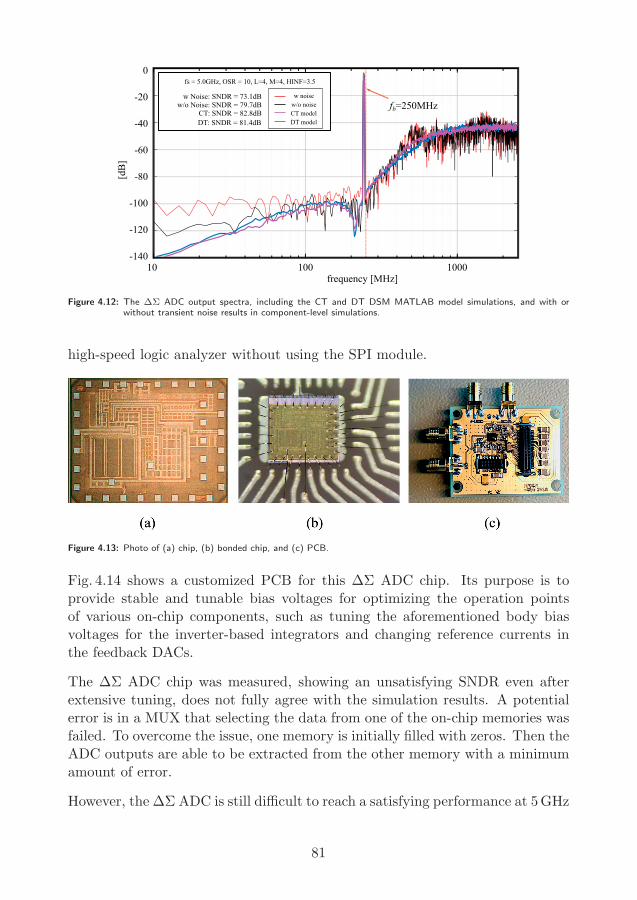
DT model
fs = 5.0GHz, OSR = 10, L=4, M=4, HINF=3.5
DT: SNDR = 81.4dB
w/o Noise: SNDR = 79.7dB w Noise: SNDR = 73.1dB
CT: SNDR = 82.8dB
w noisew/o noiseCT model
100010010frequency [MHz]
[dB
]
0
-20
-40
-60
-80
-100
-120
-140
fb=250MHz
Figure 4.12: The ΔΣ ADC output spectra, including the CT and DT DSM MATLAB model simulations, and with orwithout transient noise results in component-level simulations.
high-speed logic analyzer without using the SPI module.
Figure 4.13: Photo of (a) chip, (b) bonded chip, and (c) PCB.
Fig. 4.14 shows a customized PCB for this ΔΣ ADC chip. Its purpose is toprovide stable and tunable bias voltages for optimizing the operation pointsof various on-chip components, such as tuning the aforementioned body biasvoltages for the inverter-based integrators and changing reference currents inthe feedback DACs.
The ΔΣ ADC chip was measured, showing an unsatisfying SNDR even afterextensive tuning, does not fully agree with the simulation results. A potentialerror is in a MUX that selecting the data from one of the on-chip memories wasfailed. To overcome the issue, one memory is initially filled with zeros. Then theADC outputs are able to be extracted from the other memory with a minimumamount of error.
However, the ΔΣ ADC is still difficult to reach a satisfying performance at 5GHz
81

Figure 4.14: A base PCB, providing bias voltages to the ΔΣ ADC chip that is stacked on.
sampling frequency. Thus, the sampling frequency was decreased to 3.3GHz forstability consideration, and coefficients are carefully tuned. Fig. 4.15 shows thetime-domain measured ADC output, with a result of (a) an 11MHz input signaland (b) a 60MHz input signal. Notice that there are already random errorscausing a significant decrease in the ADC performance.
sample count
(a)
(b)
0 100 1000200 300 400 500 600 700 800 900
0 100 1000200 300 400 500 600 700 800 900
AD
C ou
tput
AD
C ou
tput
0000
1111
0000
1111
Figure 4.15: Measured time-domain ADC digital output, with the ΔΣ ADC fed with (a) an input of 11MHz and (b) aninput of 60MHz, sampled at 3.3 GHz.
82
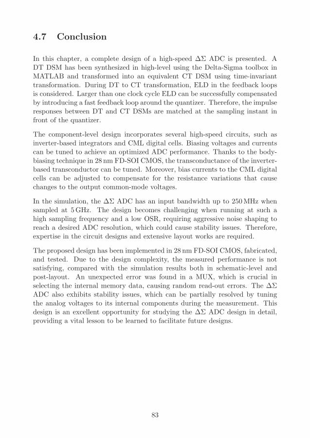
4.7 Conclusion
In this chapter, a complete design of a high-speed ΔΣ ADC is presented. ADT DSM has been synthesized in high-level using the Delta-Sigma toolbox inMATLAB and transformed into an equivalent CT DSM using time-invarianttransformation. During DT to CT transformation, ELD in the feedback loopsis considered. Larger than one clock cycle ELD can be successfully compensatedby introducing a fast feedback loop around the quantizer. Therefore, the impulseresponses between DT and CT DSMs are matched at the sampling instant infront of the quantizer.
The component-level design incorporates several high-speed circuits, such asinverter-based integrators and CML digital cells. Biasing voltages and currentscan be tuned to achieve an optimized ADC performance. Thanks to the body-biasing technique in 28 nm FD-SOI CMOS, the transconductance of the inverter-based transconductor can be tuned. Moreover, bias currents to the CML digitalcells can be adjusted to compensate for the resistance variations that causechanges to the output common-mode voltages.
In the simulation, the ΔΣ ADC has an input bandwidth up to 250MHz whensampled at 5GHz. The design becomes challenging when running at such ahigh sampling frequency and a low OSR, requiring aggressive noise shaping toreach a desired ADC resolution, which could cause stability issues. Therefore,expertise in the circuit designs and extensive layout works are required.
The proposed design has been implemented in 28 nm FD-SOI CMOS, fabricated,and tested. Due to the design complexity, the measured performance is notsatisfying, compared with the simulation results both in schematic-level andpost-layout. An unexpected error was found in a MUX, which is crucial inselecting the internal memory data, causing random read-out errors. The ΔΣADC also exhibits stability issues, which can be partially resolved by tuningthe analog voltages to its internal components during the measurement. Thisdesign is an excellent opportunity for studying the ΔΣ ADC design in detail,providing a vital lesson to be learned to facilitate future designs.
83


Chapter 5
ΔΣ ADC with DigitalBackground Calibration
5.1 Introduction
In the previous chapter, a ΔΣ ADC has been extensively studied. In thischapter, the ADC performance degradation caused by DAC non-idealities isaddressed.
Recall that in a ΔΣ ADC, a feedback loop exists. The digital signal from thequantizer output is fed back into the LF using DACs. Among all the feedbackDACs, the linearity of the outer-most DAC is essential since it behaves as anadditional input to the DSM. Any non-linearity issue can not be shaped by thehigh loop gain, which increases signal distortions seen from the output. In asimple single-bit DSM, the DAC is perfectly linear since the feedback signal iseither a plus or a minus reference voltage. While in a ΔΣ ADC architecturewhere multi-bit DACs are used, linearizing the DACs becomes a challenge thatmay require a large chip area and high power consumption.
In a multi-bit DAC, unit cell matching is one of the dominant factors for goodlinearity. Seen from a higher-level perspective, the DAC requires its linearitybetter than the overall modulator, even though it only has a limited numberof bits [61]. There are many methods to linearize the DAC. The static DACcalibration can be performed in the analog domain, that the current sourcecurrents are fine-tuned as presented in Section 4.5 in Chapter 4.
Another commonly used method is the dynamic element matching (DEM) tech-
85

nique, which is beneficial to eliminate distortion tones at the expense of addi-tional noise [12]. The Data Weighted Averaging (DWA) and Individual LevelAveraging (ILA) are algorithms to randomize the selection of the unit cells,so that mismatch error is first-order shaped. However, the DEM is less effect-ive when the OSR is low [62], which may require a second-order DEM and amodified NTF for better performance [63].
For low OSR designs, the DAC calibration is an alternative method that uses alow-cost digital core to estimate and calibrate the individual DAC unit cells, asproposed in [64]. The digital approach is attractive since it avoids the lineariza-tion block such as DEM in-the-loop, and all the estimation and calibration areperformed in the digital domain. The DAC can be implemented using small-sized devices, which further reduces power consumption.
This chapter presents a ΔΣ ADC design, using a digital calibration methodsimilar to [64]. A single chip is designed by integrating a ΔΣ ADC core and thedigital calibration core on the same chip in 65 nm CMOS. The digital circuitsare synthesized in Synopsys Design Compiler (www.synopsys.com) and placed-and-routed using Cadence SoC Encounter.
5.2 ΔΣ ADC Architecture
The proposed ΔΣ ADC is built using CIFB architecture, which means thefeedback signals are injected into the inputs of each of the integrators in theLF. The synthesized NTF is:
NTF =(z − 1)(z2 − 1.908z + 1)
(z − 0.1808)(z2 − 0.02173z + 0.08153)(5.1)
which is further mapped to an equivalent CT architecture using time-invarianttransformation similar to the approach presented in SectionA.2.1 in AppendixA.
The proposed CT ΔΣ ADC architecture is shown in Fig. 5.1. Comparing withthe DT CIFB architecture illustrated earlier in Fig. 4.1(a), the second DAC isomitted, replaced by a direct feed-forward path K2 from the first integratoroutput to a summation node to sum the second integrator and the DAC3 out-puts. This feed-forward path yields a lower signal swing at the first integratoroutput due to the lack of subtraction with the feedback signal and reduces thetotal ADC power consumption. Still, mathematically, all the coefficients in thestandard CIFB architecture in Fig. 4.1(a) can be accurately mapped.
86
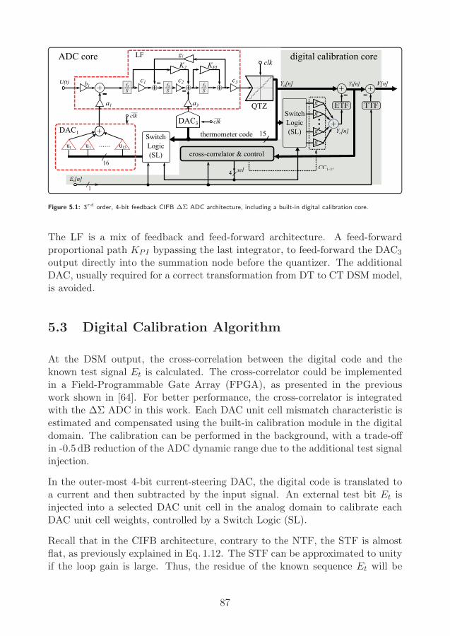
...
CC1~15
QTZ
......
16
Et[n]
SwitchLogic(SL)
DAC1
U(t)
-
K2
g1
-- -
DAC3
clk
clk
LF
a3
thermometer code 15
cross-correlator & control
TTF- -
sel
Yd[n] Yt[n] V[n]
Yc[n]
1
4
ut u1 u15
a1clk Switch
Logic(SL)
g
g
g
g
ETF TTF
SfS
KPI
c3c1 c2b1
ADC core digital calibration core
SfS
SfS
Figure 5.1: 3rd order, 4-bit feedback CIFB ΔΣ ADC architecture, including a built-in digital calibration core.
The LF is a mix of feedback and feed-forward architecture. A feed-forwardproportional path KPI bypassing the last integrator, to feed-forward the DAC3
output directly into the summation node before the quantizer. The additionalDAC, usually required for a correct transformation from DT to CT DSM model,is avoided.
5.3 Digital Calibration Algorithm
At the DSM output, the cross-correlation between the digital code and theknown test signal Et is calculated. The cross-correlator could be implementedin a Field-Programmable Gate Array (FPGA), as presented in the previouswork shown in [64]. For better performance, the cross-correlator is integratedwith the ΔΣ ADC in this work. Each DAC unit cell mismatch characteristic isestimated and compensated using the built-in calibration module in the digitaldomain. The calibration can be performed in the background, with a trade-offin -0.5 dB reduction of the ADC dynamic range due to the additional test signalinjection.
In the outer-most 4-bit current-steering DAC, the digital code is translated toa current and then subtracted by the input signal. An external test bit Et isinjected into a selected DAC unit cell in the analog domain to calibrate eachDAC unit cell weights, controlled by a Switch Logic (SL).
Recall that in the CIFB architecture, contrary to the NTF, the STF is almostflat, as previously explained in Eq. 1.12. The STF can be approximated to unityif the loop gain is large. Thus, the residue of the known sequence Et will be
87

visible in the quantizer output: Yd. Therefore, the DAC unit cell characteristicsare estimated by calculating the cross-correlation between the Yd and the Et.
The calibration relies on cross-correlation, as presented in [65]. The cross-correlator & control module shown in Fig. 5.1, which calculates the cross-correlationbetween Et and Yt and generates a set of calibration coefficient CCi. The blockdiagram of the cross-correlator & control module is shown in Fig. 5.2.
SL summation
DFF division
CCF calculator
Yd
Et
Yt V
Yc
CCFi
CCi
calibrator
calculator
DFF
DFFTTF
DFFETF
DFF
Figure 5.2: Block diagram of the cross-correlator & control module.
During estimation, first, the cross-correlation factor CCFi for ith unit cell inDAC1 is calculated, which is:
CCFi =
L∑n=1
Et[n] · Yt[n] ≈ ki · s2Et, i = t, 1, 2, ..., 15 (5.2)
where, ki is the individual gain of the unit element under test, and s2Etis the
variance of the known test signal Et. The L is the number of samples forcalculating cross-correlation, which is 218 that proved to be sufficient for properlycharacterizing the DAC linearity.
The next step is to calculate the calibration coefficient of CCi for each of theDAC unit cells. Note that there is one additional feedback DAC unit Ut in theDAC1, which provides a calibration reference for the rest unit cells, and replacesa specific unit cell under test that avoids disturbing the DAC1 operation duringcalibration.
The CCi is calculated based on the division between the CCFi and the referenceCCFt, which is:
CCi = k(CCFi
CCFt− 1), i = 1, 2, ..., 15 (5.3)
During calibration, the 15-bit thermometer code Yd from the quantizer output
88

is multiplied by the CC in bit-wise, which is:
Yc =
15∑i=1
Yd[i] · CCi (5.4)
The Yc passes through an Error Transfer Function (ETF), then subtracted bythe Yd, and becomes the calibrated ADC digital output Yt. The Yt is fed-backto the cross-correlator for iteratively refining its value. Finally, the test signalEt passed through a Test Transfer Function (TTF) and subtracted by Yt. TheETF and TTF are pure delays in this design, since the STF is flat, and theerror and test signal are injected into the system with the same path as theinput signal U .
The calibrated ADC output V becomes:
V [n] = Yd[n]− Yc[n] · ETF − Et[n] · TTF (5.5)
5.4 Component-Level Implementation
A design has been implemented in 65 nm CMOS to verify the concept of di-gital calibration. The DSM core is built with 3rd order, 4-bit output CIFBarchitecture, shown earlier in Fig. 5.1. The synthesized digital core, using cross-correlator to process the ADC output Yd and the known pseudo-random testsequence Et, is placed on the same chip. The CCF for each of the ADC outputbits is calculated and stored in the internal memory. The digital calibrationmodule is synthesized and laid out in the same chip as the DSM core, withmanually drawn connection wires between them.
5.4.1 DAC Unit Cell Design
The chosen DAC unit cells are based on resistive current-mode DAC. The res-istor is used to generate a current into the LF summation node, which is thevirtual ground node of the integrator, in response to the digital codes presentedon their input bit lines. Compared to the widely used current-steering DAC,the resistive DAC shows less noise [54].
The unit cell schematic is shown in Fig. 5.3. The DFF drives an inverter con-sisting of P8 and N8, and then convert the reference voltages to current by theresistor R. The DFF is built by two latches which are connected in series, up-dating the signal Q from the digital input D at the clk rising edge. The inverter
89

is connected to either Vref+ or Vref− controlled by Q. Lastly, the DAC unitcell’s output current Iout is the current flowing through the resistor R [66]. Thedirection Iout is controlled by the inverter, which either from Vref+ to A or theother way.
D
N1
N2
vdd
vdd
P1
P2ClkI
ClkN
ClkN
ClkI
ClkN
ClkIINV3
vdd
ClkI
ClkN
Vref+
RQ
Clk ClkIClkN
latch 1 latch 2
clk =0signal path
clk =1signal path
DFF
+Iout
-Iout
A
N3
N4
P3
P4
P5
N5
N6
N7
P6
P7
INV4
INV1
INV2
INV5 INV6
N8
P8
Vref-
Figure 5.3: The resistive DAC unit cell schematic.
The differential DAC1 and DAC3 share an identical layout, but different in thepurpose of each unit cell, which is shown in Fig. 5.4. In the DAC layout, theDAC unit cells are placed next to each other. In DAC1, two of the unit cellsat the edges are used for pseudo-random test sequence injection for calibrationpurposes. In DAC3, dummy unit cells are added to both sides of the DAC unitcell array to mitigate the difference of diffusion under the resistors between theouter and inner unit cells [49]. Thus, the DAC unit cell matching is preservedif the mismatches between the resistors are minimized.
5.4.2 Switch Logic Design
For calibration purposes, the digital code to the outer-most DAC1 is re-routedby an array of switches: a SL, which re-routes the thermometer codes fromthe quantizer to the outer-most DAC. Fig. 5.5(a) shows the schematic of theswitches, which is controlled by a Read-Only Memory (ROM): switch ROMthat generates a 30-bit predefined control signals c0 to c29 to the switches. Thelayout of the switch ROM is shown in Fig. 5.5(b), and the layout of switches isshown in Fig. 5.5(c).
By selecting a predefined c from the switch ROM using the external digital con-trol bits, the test bit DinT is injected into one of the selected DAC1 unit cells. Inthe meantime, the last unit cell is selected to maintain the ΔΣ ADC operation.
90

digital input
current output
resistors
DFFs
inverters
30 DAC unit cells (differential signal)unit celldummy
unit celldummyDAC3
30 DAC unit cells (differential signal)test bitDAC1
differential
Figure 5.4: 4-bit differential DAC layout.
For example, by default, the DinT is injected into the bit line DoutT to the testunit cell. The 15 input bit line Din0−14 are connected to the Dout0−14, respect-ively. For testing the DAC unit cell 0, c0 reconnects the Din0 to DoutT , and DinT
is connected to the Dout0. The rest bits remain unchanged. By cycling the DinT
through all the 15 DAC unit cells, the correlation-based estimator implementedin the digital domain can effectively estimate the mismatches between the DACunit cells in the outer-most DAC.
91

from comparator
from switch ROM
switches
to outer-most DAC
A B CA B
Din0DinT
A B C A BA B C
Din1 Din2 Din13 Din14
Dout0 Dout1 Dout2 Dout13 Dout14DoutTswitches
Din from comparatorDinT from external
Dout toouter-most DAC
c0 c1 ,c2 c3 ,c4 c5 ,c6 c27 ,c28 c29c from switch ROM
-c29
digi
tal c
ontro
l bits
switch ROM
(c)
(a) (b)
c0
Figure 5.5: The SL design, (a) shows the schematic of switches, (b) shows the layout of switch ROM, and (c) shows thelayout of switches.
5.4.3 Quantizer Design
The quantizer is a core block for converting the signal from the analog domain tothe digital domain. The delay between the clocking edge and the stable digitaloutput codes is critical since the quantizer is placed inside the feedback loop.The Flash ADC is one type of ADC that is fast in performing A/D conversion,which is suitable to be the core in a quantizer architecture.
The four-bit flash quantizer schematic is presented in Fig. 5.6, which consists of15 comparators. Each comparator receives its reference voltage from a resistorladder. The resistor ladder divides a high reference voltage and the ground into15 pairs of reference voltages, of which the high reference voltage is bufferedfrom an external reference voltage Vref . In contrast, the low reference voltageis the voltage that appears on the bottom resistance Rfoot. The differentialinput signal Vinp and Vinm are connected to the plus and the minus terminals,respectively, in all the 15 comparators.
The comparator schematic is shown in Fig. 5.7. In the pre-amplifier,the differ-ence between the differential input signal, Vinp and Vinm, and differential refer-ence voltages, Vrefp and Vrefm, is amplified. The pre-amplifier outputs Vampp
and Vampm are latched by a dynamic cross-coupled inverter latch [67]. During
92

Vref +- +
+--
regen.clk
Vinm
R7pcomparator 13
comparator 14b14
Vinp
R6p
R5p
R7mRfoot
latchSR
latch
clk
pre-++--amplifier
b13
comparator 0b0regen.
latchSR
latchamplifier
++--
pre-clk
Figure 5.6: 4-bit quantizer schematic.
the clk low pulse, the regenerative latch is in reset mode so that the Sint andRint are reset to the supply voltage vdd. During the clk high pulse, the regen-erative latch is in latch mode that the pre-amplifier’s outputs are latched andstored in the SR latch. The SR latch acts as a memory device that maintainsthe comparison results for one clock period.
N1 VrefmVrefpVinp
Vb Vb
vdd
vdd
Sint
Rint
S
R
Sint Rint
clkINV1
SR latch regenerative latch
V ampm
Vinm
V ampp
R1 R2
N2 N5
N3
N4
N6
N8N7
N9 N10
N11 N12
P1
P2 P3
P4
INV2
INV3 INV4
Dp
Dm
clk
clk
pre-amplifier
Figure 5.7: Comparator schematic.
5.4.4 Amplifier Design
The amplifiers are critical components in an active-RC integrator, used through-out this design. The first integrator in the LF requires high linearity as anynon-linearity in this stage directly degrades the ΔΣ ADC accuracy. The ampli-fier used in the last integrator requires a high driving capability due to a largeinput capacitance in the multi-bit quantizer.
In this ΔΣ ADC design, the amplifiers share the same two-stage, Miller-compensated,class-AB output architecture [14]. The bias current in each amplifier is uniquefor balancing the speed, area, and power consumption.
93

Fig. 5.8 shows the amplifier schematic. An external bias current Iref is injectedinto the bias circuit and mirrored into the tail current sources Nb1 and Nb2, whichare cascoded to provide a stable bias current. The common-mode voltage of theoutputs Voutp and Voutm are sensed by a Common-Mode Feedback (CMFB)circuit, which controls a part of the PMOS transistors in the input differentialstage active load.
Vinm
Vcmfb
VoutmVbN Vb1
Vb2
Vcmref
VcmfbIrefCcm
N1m
Nb1
P3m
N2m
C1m
Rzm
R1m
Vdd CMFB circuitbias circuit
Vinp
Vb2Nb2
P2m P1m
VbP
P1p P2p
VbP
N1p
N2pR1p
VbN
Voutp
C1p
Ccp
P3p
RzpRbias
VbP
Voutm
Voutp
Vb1VbN
Figure 5.8: OP-amplifier schematic, includes a bias circuit and a CMFB circuit.
The first amplifier has the highest linearity requirements, and the last amplifierhandles the KPI path that needs to be fast, while the second integrator has thelowest GBW requirement. The optimized simulated GBW of the three amplifiersare 600, 350, and 600MHz, respectively.
5.5 Simulation and Measurement Results
The design was implemented in 65 nm CMOS and has been simulated in theSpectre simulator in Cadence. The effectiveness of the proposed digital calibra-tion method is evaluated by introducing mismatches in DAC, based on Monte-Carlo simulation results, and then estimated and calibrated. Fig. 5.9 shows theADC output spectra with an input sine wave at 2MHz. Assume 2% unit ele-ment mismatch appear in the outer-most DAC, without calibration, the SNDRis 55.7 dB, and large distortion tones are visible. By injecting a pseudo-randomtest sequence Et into the system and cycle through all the unit cells, the calib-rated system shows a much improved SNDR of 69.2 dB, close to the well-matchedsystem that has a simulated SNDR of 70.0 dB.
Fig. 5.10 shows the microscopic photo of the fabricated chip. The ΔΣ ADC coreand the digital calibration block are overlaid with their layouts, respectively.The chip size is 1mm2, of which 420 um×320 um is for the ΔΣ ADC core, and
94

frequency [MHz]
[dB]
before calibrationwith calibration after 3 iterationswithout mismatch (ideal)wwb
mia
da
without mismatch (ideal)w m d
1 10-120
-100
-80
-60
-40
-20
0
HD3: -91dB HD3: -85dB HD2: -81dB
HD2: -60dB HD3: -75dB HD4: -72dB
signal bandwidth fb
SNDR=55.7dB, SFDR=56.5dBSNDR=69.2dB, SFDR=77.4dBSNDR=70.0dB, SFDR=85.3dB
Figure 5.9: ADC output spectra of: Before and after calibration when DAC mismatch appears, and the ideal simulationresult.
200 um×470 um is for the digital calibration core. The chip is bonded to acustomized PCB, as shown in Fig. 5.11, and measured.
Figure 5.10: Chip microscopic photo, layout of ΔΣ ADC core and digital calibration core.
The post-layout simulation and the measurement results are plotted in Fig. 5.12.The post-layout simulation shows an SNDR of 65.5 dB and an SFDR of 77.4 dB,which degrades from an SNDR of 69.6 dB and an SFDR of 80.6 dB in a CT modelsimulation in MATLAB, partially due to increased thermal noise.
95
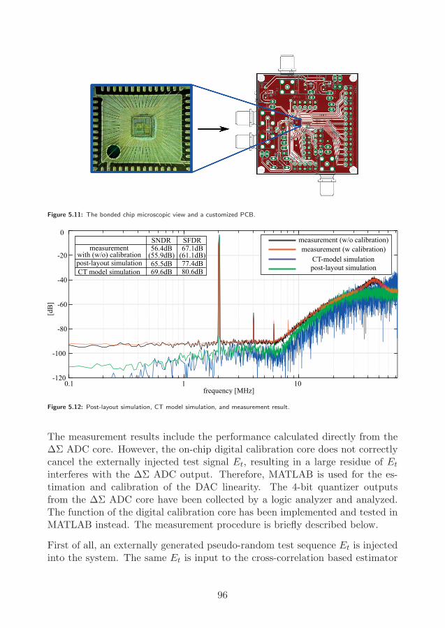
Figure 5.11: The bonded chip microscopic view and a customized PCB.
frequency [MHz]1010.1
-120
-100
-80
-60
-40
-20
0
[dB
]
post-layout simulationCT model simulation
SNDR
(55.9dB)65.5dB69.6dB
measurement with (w/o) calibration
56.4dBSFDR
(61.1dB)67.1dB
77.4dB80.6dB
CT-model simulationpost-layout simulation
measurement (w/o calibration)measurement (w calibration)
Figure 5.12: Post-layout simulation, CT model simulation, and measurement result.
The measurement results include the performance calculated directly from theΔΣ ADC core. However, the on-chip digital calibration core does not correctlycancel the externally injected test signal Et, resulting in a large residue of Et
interferes with the ΔΣ ADC output. Therefore, MATLAB is used for the es-timation and calibration of the DAC linearity. The 4-bit quantizer outputsfrom the ΔΣ ADC core have been collected by a logic analyzer and analyzed.The function of the digital calibration core has been implemented and tested inMATLAB instead. The measurement procedure is briefly described below.
First of all, an externally generated pseudo-random test sequence Et is injectedinto the system. The same Et is input to the cross-correlation based estimator
96
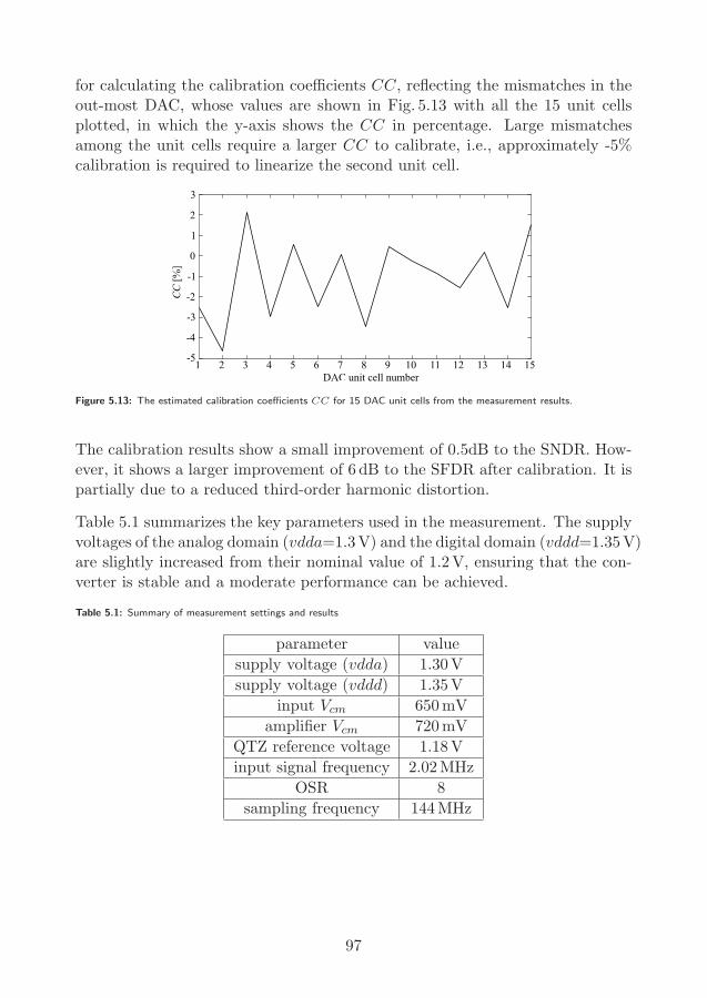
for calculating the calibration coefficients CC, reflecting the mismatches in theout-most DAC, whose values are shown in Fig. 5.13 with all the 15 unit cellsplotted, in which the y-axis shows the CC in percentage. Large mismatchesamong the unit cells require a larger CC to calibrate, i.e., approximately -5%calibration is required to linearize the second unit cell.
DAC unit cell number1 2 3 4 5 6 7 8 9 10 11 12 13 14 15-5
-4
-3
-2
-1
0
1
2
3
CC
[%]
Figure 5.13: The estimated calibration coefficients CC for 15 DAC unit cells from the measurement results.
The calibration results show a small improvement of 0.5dB to the SNDR. How-ever, it shows a larger improvement of 6 dB to the SFDR after calibration. It ispartially due to a reduced third-order harmonic distortion.
Table 5.1 summarizes the key parameters used in the measurement. The supplyvoltages of the analog domain (vdda=1.3V) and the digital domain (vddd=1.35V)are slightly increased from their nominal value of 1.2V, ensuring that the con-verter is stable and a moderate performance can be achieved.
Table 5.1: Summary of measurement settings and results
parameter value
supply voltage (vdda) 1.30V
supply voltage (vddd) 1.35V
input Vcm 650mV
amplifier Vcm 720mV
QTZ reference voltage 1.18V
input signal frequency 2.02MHz
OSR 8
sampling frequency 144MHz
97

5.6 Conclusion
In this chapter, a ΔΣ ADC with background calibration is explained. Thesimulation results are illustrated, and the chip measurement results are shown.
This work presents a digital calibration technique in CT ΔΣ ADC. The converteris clocked at 144MHz, with an OSR of only 8. Non-idealities in outer-most DACare measured and removed in the background by a digital calibration core, whichis implemented in a single chip together with the ΔΣ ADC core.
The digital calibration is an attractive method for efficiently improving the ΔΣADC linearity when the tuning in the analog domain is not feasible. The cross-correlation method does not involve large power consumption and chip areaoverhead, which can be placed aside with the ADC core.
Besides, low OSR ΔΣ ADC does not allow the randomized method for linear-izing the DAC. The digital calibration method presented in this research showsa feasible solution to low OSR designs.
A test chip has been implemented in 65 nm CMOS and measured. Even thoughthe integrated digital calibration module for calibrating the outer-most DACin the digital domain does not work as expected, the MATLAB calibrationmodule still proves that the distortion tones can be partially reduced using theproposed algorithm. As a result, an improvement to the SFDR of the converteris observed.
98

Chapter 6
Summary of Included Papersand Author Contributions
Paper I:Digital Background Calibration in Continuous-timeΔΣ Analog to Digital Converters
Summary
This paper presents a research work of a CT Delta-Sigma A/D converter that isdesigned, simulated, and implemented in 65 nm CMOS. The converter is clockedat 144MHz with a low OSR of only 8. The low OSR imposes low efficiency forthe DEM to linearize the DAC, thus requiring a background digital calibrationtechnique. A digital background calibration core is designed and integrated withthe ADC in a system-on-chip solution to measure and then remove non-idealitiesin the outer-most multi-bit feedback DAC in the background.
This paper presents the architecture and circuit level design of a third-order,four-bit feedback, single-loop CT Delta-Sigma ADC. The digital implementationand mathematical calculations have been explained for showing the effectivenessof linearizing the DAC in a low OSR Delta-Sigma ADCs. The maximum simu-lated SNDR is 67.1 dB within 9MHz signal bandwidth.
99

Author Contributions
I have designed, simulated, and chip-level implemented the CT Delta-SigmaADC in 65 nm CMOS. I was partially involved in developing the digital calibra-tion core. I carried out the top-level layout of integrating the Delta-Sigma ADCcore and the digital calibration core, designed in separate circuit design tools,into a single chip.
Paper II:A continuous-time delta-sigma ADC with integrateddigital background calibration
Summary
This paper is an extended version of paper I, with detailed descriptions of thecomponent-level implementation of the proposed digital background calibrationtechnique. Compared with paper I, the detailed digital circuit implementationis presented. The division block implementation based on the Newton-Raphsonequation is described, and the utilization of clock gating for saving dynamicpower dissipation is presented.
The component-level implementations of the core building blocks in the pro-posed third-order, four-bit feedback, single-loop CT Delta-Sigma ADC, suchas amplifiers, Flash quantizer, and DAC, are presented in this research paper.The converter simulation results are shown, and the effectiveness of the digitalbackground calibration block is verified.
Author Contributions
I have drawn new figures to represent the individual block schematics in theDelta-Sigma ADC and explained the operations of the digital background cal-ibration core. I have presented the DT to CT conversion using mathematicalequations and carefully organized the paper for an enhanced illustration.
100

Paper III:A 5 GHz CT ΔΣ ADC with 250MHz Signal Band-width in 28 nm-FDSOI CMOS
Summary
This paper presents a continuous-time Delta-Sigma ADC designed and simu-lated in 28 nm FD-SOI CMOS. The ADC is clocked at 5GHz with a signalbandwidth of 250MHz, for an OSR of only 10. A 4th order loop filter is adoptedto enhance quantization noise shaping in the presence of a low OSR. The excessloop delay exceeds one clock cycle, requiring two additional feedback paths torestore the nominal noise transfer function.
The conversion from a high-level model to component-level implementation hasbeen presented in this research paper. The Delta-Sigma ADC design is shownthat includes multiple high-speed design methodologies for achieving an optim-ized design for use in high-performance base stations in the future. The loopfilter is built with inverter-based integrators, and the transistors are tuned byadjusting body-biasing voltages. The current-mode logic is used in the digitalpart to improve the signal transition speed. The Delta-Sigma ADC has a sim-ulated SNDR of 73.1 dB for a power consumption of 232mW in simulation.
Author Contributions
I designed, simulated, and laid-out the complete Delta-Sigma ADC core in 28 nmFD-SOI CMOS. I studied the state-of-the-art high-performance Delta-SigmaADCs and utilized the fast-speed inverter-based integrators in the design basedon the suggestions from my supervisors. I calculated the transformation fromDT to CT ADC architecture using impulse-invariant transformation, with theconsiderations of the different excess loop delays in the ADC loop.
I synthesized and placed-and-routed the SPI module, using a source code providedby Ericsson Research, Ericsson AB, Lund, Sweden. I study the controllingmethod of this SPI module for controlling the on-chip memory that collectingthe data from the Delta-Sigma ADC’s output and reading-out the stored datain slow-speed sequentially. I managed to integrate the memory into the samechip design and connected it to the Delta-Sigma ADC core. I also designed thePCB for this ADC chip and soldered the components on the manufactured PCBfor measurements (measurement results are not shown in the attached paper).
101

Paper IV:A 10-bit Split-Capacitor SAR ADC with DAC Imbal-ance Estimation and Calibration
Summary
This paper presents a 10-bit SAR ADC core design sampled at 200MS/s. To re-duce area and power consumption, the ADC adopts a split-capacitor DAC. Thegain error is estimated by injecting a PRBS signal into the equal-weighted capa-citors on each split capacitor array and detected at the ADC output. The DACimbalance estimation and correction in the proposed SAR ADC is performed byan off-chip post-processor developed in MATLAB.
This paper shows a practical way of estimating and calibrating the DAC-imbalancein a split capacitor array and shows the capabilities of being placed in a largerTime-Interleaved SAR ADC architecture. The presented SAR ADC core lies ina 7-channel Time-Interleaved SAR ADC chip, which has been designed and fab-ricated in a 22 nm FD-SOI CMOS process. A single SAR ADC core achieves anSNDR of 48.7 dB and an SFDR of 66.7 dB for input frequencies up to samplingfrequency. The power consumption is 4.3mW, and the FoMs is 152 dB.
Author Contributions
In this work, I learned the functionality of different measurement tools in the lab.I performed the measurements of the fabricated SAR ADC, previously designedand taped-out by Ericsson Research, Ericsson AB, Lund, Sweden. I was involvedin the designs of the DAC imbalance estimation and calibration post-processorin MATLAB, to estimate and calibrate the bridge attenuation coefficient inthe split capacitor architecture. I wrote this paper based on simulation andmeasurement results.
102

Paper V:Asynchronous vs. Synchronous CMOS SAR ADCs -A Comparison
Summary
In this paper, an improved 10-bit ASAR ADC core has been implemented basedon the 10-bit SSAR ADC design. Similar to the previous SSAR design, sevenASAR sub-ADC cores are time-interleaved, designed, and simulated in 22 nmFD-SOI CMOS. The schematic of the ASAR ADC control logic is shown andcompared with the SSAR ADC control logic schematic.
The two ADCs are compared in this paper, in terms of design robustness andcircuit speed, in the same technology node and under a similar simulation test-bench. In the ASAR ADC, the maximum sampling frequency for nominal SNDRperformance, assessed both with and without transient noise, is slightly higher.The ASAR ADC displays a graceful SNDR degradation as the sampling fre-quency increases further instead of an abrupt SNDR collapse in the SSAR ADC.Together with the benefits of a lower external clock frequency, this establishesthe superiority of the ASAR ADC, with only a minor increase in design com-plexity.
Author Contributions
In this work, I did the schematic and the layout design of the ASAR ADC, witha reference of the previously designed SSAR ADC. The ASAR ADC chip hasalready been manufactured in 22 nm FD-SOI CMOS. I performed extensive sim-ulations for comparing the ASAR ADC and the SSAR ADC and concludes theoverall superiority of ASAR ADC. I synthesized an on-chip memory componentusing the scripts in the earlier design and built an interface circuit between theASAR ADC and the memory. I have analyzed the component-level simulationsand achieved satisfying results. Lastly, I was partially involved in the PCBdesign of this chip. The chip will be measured as soon as the PCB is ready, anda suitable lab is available.
103
Paper VI:A Design Method to Minimize the Impact of Bit Con-version Errors in SAR ADCs
Summary
This paper analyzes the bit conversion errors in high-speed SAR ADCs andproposes a design method to minimize their impact on ADC performance. Byclosely examining the existing design, the cause of bit conversion errors occursin SAR ADCs are found. Due to the parallel signal processing paths of thecomparator differential outputs in the existing design, large Sparkle-code errorsoccur that suspends the current and the subsequent charge redistribution in theCDAC. Besides, the use of SR latch in the SAR comparator may cause errorsif the previous decisions are not updated before latched by the following digitalcontrol logic. All these bit conversion errors cause abrupt SNDR degradationwhen the SAR ADC sampling frequency increases.
The proposed improved SAR ADC design removes the SR latch from the out-put stage of the differential comparator. While using only a single-ended com-parator output to generate the differential signals for the internal capacitiveDAC, sparkle-code errors are avoided, and conversion errors from a previous bitconversion due to memory effects in the SR latch are eliminated. The 10-bitsynchronous SAR ADC has been modeled in MATLAB and subsequently im-plemented at the circuit level in a 22 nm FD-SOI CMOS. The improved SARADC shows a graceful SNDR degradation at increased sampling frequencies,vastly improving the ADC performance compared to when sparkle-code errors,or conversion errors due to an invalid comparator output, are allowed to occur.
Author Contributions
In this work, I simulated the SAR ADC circuit and pinpointed an issue thatSparkle-code errors maybe generated from the invalid CDAC control codes. Icreated a MATLAB model to understand the root cause of the problem andimproved the previous SAR ADC design based on the analysis. I ran extensivesimulations to confirm that removing the SR latch and processing a single-endedcomparator’s output improves the circuit robustness, causing CDAC’s chargeredistribution to a default direction whenever a bit conversion error occurs.
104

Chapter 7
Conclusion and Future Work
The bandwidth increase in communication systems imposes enormous demandson the performance of their building blocks. The ADC is one of the criticalblocks in communication devices that advanced rapidly in the previous decades.The emerge of the 5G network requires high-speed, high-performance ADCs,an attractive topic in research and industry. In this research work, two SARADCs and two ΔΣ ADCs have been designed in component-level, simulated, andfabricated in the advanced CMOS technologies. The ADC architectures havebeen shown, the detailed circuit designs have been explained, and tunability tocounter react the non-idealities in the ADCs due to the Process, Voltage, andtemperature variations, have been addressed. The benefits and drawbacks ofeach design have been explained.
The SAR ADCs belong to the Nyquist-rate ADC category, which is very at-tractive due to their digital friendly architecture and time-interleaving capab-ility. The split-capacitor array in the CDAC in a SAR ADC is an attractivetechnique to reduce the total capacitance. As a result, the loads to the drivingswitches are decreased to reduce the SAR ADC’s power consumption. How-ever, influenced by parasitic capacitance, an imbalance between the two DACarrays in the split-capacitor CDAC appears, limiting the maximum ADC resol-ution. Thus, the DAC imbalance estimation and calibration are performed in apost-processor in the digital domain, currently implemented using MATLAB.
A reference SSAR ADC design uses an external high-speed clock to synchronizethe SAR ADC’s internal comparator and its digital control logic. The SARcontrol logic design can be implemented using digital cells, but the trade-offis higher power consumption and the potential risk of experiencing high-weight
105

bits conversion errors due to insufficient comparison time. In contrast, an ASARADC is designed based on the experiences gained from the SSAR ADC design.It dynamically generates an internal clock to the comparator, guaranteeing high-weigh bits to be correctly converted, showing a graceful SNDR degradation ata higher sampling frequency than the synchronous version.
In the presented work, two ΔΣ ADCs are designed. ΔΣ ADCs belong tothe oversampled ADC category, which is challenging when operated in a highsampling frequency for a moderate signal bandwidth. One of the designs is ahigh-speed ΔΣ ADC, implemented in 28 nm FD-SOI CMOS. This ADC designincorporates various techniques for achieving high-speed, such as inverter-basedintegrators in the loop-filter and current-mode logic in the digital logic. Largerthan one clock cycle excess loop delay is compensated by introducing a directfeedback loop using an un-clocked DAC around the quantizer.
The second design evaluates the effectiveness of a digital background calibrationtechnique, which is a ΔΣ ADC clocked at 144MHz with a low OSR of only 8.A pseudo-random test sequence is injected and cycled through all the DACunit cells, and the cross-correlation between the ADC output and the knownsequence is calculated in the digital domain. A digital calibration circuit andthe ΔΣ ADC are combined and implemented in a single chip in 65 nm CMOS,simulated and measured.
The future ADC designs can be inspired by the analysis presented in this dis-sertation, to design a high-performance ADC that will be implemented in asophisticated larger system. One choice is improving the single-channel SARADC’s performance and time-interleaving a larger number of channels for anwiden bandwidth and increased ADC resolution. Another choice is to designa high-performance ΔΣ ADC, which will still be an interesting topic in theforeseeable future. For reaching wide-bandwidth and high-accuracy at the sametime, high-order and aggressive noise shaping are inevitable. The current designalready involves extensive tuning both in analog and in the digital domain. Thenew design will be optimized for better robustness and stability in terms ofarchitecture selection and partially self-calibration, targeting high-speed, high-accuracy applications. Furthermore, Pipeline ADCs are very attractive, whichalready show huge potentials in communication devices and will be studied inthe future.
106

Appendix


Appendix A
Coefficient Calculations in DTto CT DSM ArchitectureTransformation with 4th OrderCRFF LF
This Appendix explains the CT DSM coefficient calculations in a 4th orderCRFF CT DSM LF, transformed from a set of coefficients from an equivalent4th order CRFF DT DSM architecture. A similar principle applies to otherDSM architectures as well.
The original DT DSM architecture is shown in Fig.A.1. It has a DAC thatfeedbacks the quantizer digital output signal into the analog domain then feed-forward to a summation node through four feed-forward paths aDT1 to aDT4.An additional feedback path gDT feeds the third integrator output signal backinto the second integrator input node, acting as a resonator.
In contrast to the DT DSM that process discrete-time signals, the transformedCT DSM architecture shown in Fig.A.2 processes the continuously varying sig-nals, meaning that the signals are changing from time to time. The method tomap the CT DSM with the original DT DSM is the impulse-invariant trans-formation [68]. The CT DSM coefficients are calculated so that the impulseresponse HCT of the open-loop filter in CT and HDT in DT DSM architectureare equivalent at the quantizer sampling instant.
An important consideration during a DT to CT DSM transformation is the
109

quantizer
DAC
Vz-1
zz-1-
gDT
aDT3
z-1z-11
z-11
HDT
step pulse
aDT4
aDT2aDT1
z-1-
summationnode
z
Figure A.1: 4th order CRFF DT ΔΣ DSM architecture.
quantizer
DAC
V
dclk
dELD3dELD2
dELD1
dELD4
gCT
aCT1
s1
HCT
step pulse
s s s
aCT2
aCT3
aCT4
aCTdly
aCTfb
1 1 1-
- --
summationnode i
when ELD >Tonly required
Figure A.2: 4th order CRFF CT ΔΣ DSM architecture, with each feed-forward loop delay included due to the finite GBWof integrators.
ELD, which is termed as a combination of the delay required for a practicalquantizer to resolve a decision and the inevitable delays in the feedback paths,including the DACs and the integrators.
The coefficients mapping from a 3rd order CIFB DT to CT DSM architecturehas been discussed in [54]. In this Appendix, the analysis extends further to a4th order CRFF CT DSM architecture. The coefficients are calculated under twodifferent lengths of ELDs: an ELD less than or equal to T ; and an ELD largerthan T . Before discussing the details of DT to CT DSM coefficient calculationsin the prior two scenarios, the original DT DSM coefficients are explained first.
A.1 The DT DSM Open-Loop Transfer Function
The proposed 4th order, single resonator CRFF DT DSM architecture, is shownin Fig.A.1. The z-domain open-loop transfer function HDT , observed from the
110

quantizer input, is:
HDT (z) =−aDT1
(z − 1)+
aDT2(z − 1− gDT z)
(z − 1)[(z − 1)2 + gDT z]
− aDT3z
(z − 1)[(z − 1)2 + gDT z]− aDT4z
2
(z − 1)2[(z − 1)2 + gDT z]
(A.1)
The Eq.A.1 is then mapped to DT domain HDT [n] using the z-transformation.The very small resonator coefficient gDT is temporarily set to zero in the follow-ing calculations, which shows a very small difference between the resulting CTDSM compared with the DT DSM. The HDT [n] is:
HDT [n] =− aDT1 − aDT2 · n− aDT3 · (n2
2− n
2)− aDT4 · [1
6· (n3 − n)] (A.2)
where the N is the sample number.
TableA.1 lists the coefficients for each term in HDT [n]:
Table A.1: Terms and coefficients in HDT [n]
HDT [n] term coefficient
n3 −aDT4
6
n2 −aDT3
2
n −aDT2 +aDT3
2+
aDT4
6
1 −aDT1
A.2 DT to CT DSM Transformation
Fig.A.2 shows a CRFF CT DSM architecture. Contrary to the CRFF DTDSM architecture, the ELDs are the important parameters for calculating the
111

coefficients. There is an additional delay when the DAC output signal is fedback to the first CT integrator input. The feedback signal then passes throughthe integrators, whose outputs are scaled and fed-forward to the summationnode through the gain paths from aCT1 to aCT4.
Note that the four feed-forward path delays may not be equal since the finiteGBW of the integrators introduce delays. These delays are described as dELD1 todELD4 in the feed-forward paths. Furthermore, a fixed delay of dclk is inevitablyadded between the quantizer and the feedback DAC. It could be set to half clockperiod delay (0.5T ), meaning that the DAC and the quantizer are clocked at theopposite clocking edges, e.g., the quantizer is clocked at the clock rising edgewhile the DAC is clocked at the clock falling edge.
Usually, such a 0.5T delay between the quantizer and feedback DACs is sufficientfor allowing the quantizer to complete a conversion, which leads to a scenariothat the ELD is less than or equal to T , which will be discussed in SectionA.2.1.
On the other hand, in a high-speed CT DSM, 0.5T may not be sufficient forreading out the properly settled quantizer outputs. A dclk close or equal to T isthe only viable choice, which eventually introduces a larger than one clock periodELD in the feedback loops after adding the dELD1 to dELD4. This scenario willbe discussed in SectionA.2.2.
A.2.1 DT to CT Transformation - ELD Less than or Equal toOne Clock Period
Typically, the ELD is not larger than T , meaning that the loop delay fromthe digital quantized signal is settled and feedback to the quantizer input nodeis within T . In this scenario, the impulse response of a CT DSM can per-fectly match to the impulse response of the original DT DSM architecture byadding one additional feedback path aCTdly to the summation node, as shownin Fig.A.2. The purpose of the aCTdly path is to match the first sample in theopen-loop impulse response of the CT to the DT DSM.
The impulse-response of the CT DSM architecture shown in Fig.A.2 is:
HCT (s) =aCT1
s+
aCT2
s2 + gCT+
aCT3
s(s2 + gCT )+
aCT4
s2(s2 + gCT )(A.3)
still, assuming gCT = 0 in the following calculations.
The DAC feedback pulses are determined first. Then, the ELDs need to beestimated to calculate the time-domain transfer function.
112

The DAC feedback pulses in the time domain are defined as rDAC , which isthe height of the feedback pulse, commonly in NRZ or in RZ shape. The twosymbols, αclk and βclk, are denoted as the DAC feedback pulse start and stoptime, respectively, compared with the quantizer sampling instant and normalizedto the T . Assume rDAC is 1 between αclk and βclk, and 0 in the other conditions,the rDAC in Laplace domain becomes RDAC :
RDAC =1
s(e−sαclk − e−sβclk) (A.4)
Based on component-level simulations, dELD1 to dELD4 are estimated. Thestart and stop times of the equivalent feedback signal, with an NRZ DAC pulsedelayed by dclk and four feed-forward paths delayed by dELD1,2,3,4, are α1,2,3,4 =dclk + dELD1,2,3,4 and β1,2,3,4. The CT DSM open-loop LF impulse response inthe time domain, including the Eq.A.4 and still disregarding the gCT path, is:
HCT a1 [n] = L−1{−aCT1
s2(e−sα1 − e−sβ1)}
=
{−aCT1(γ1 − α1) n = 1
−aCT1(β1 − α1) n ≥ 2
(A.5)
where γ1 = min{1, β1} when the DAC feedback pulses are extended beyond oneclock period.
Similarly, the inverse Laplace transformation for the rest of the paths are:
HCT a2 [n] = L−1{−aCT2
s3(e−sα2 − e−sβ2)}
=
{−aCT2[(γ2 − α2) +
α22−γ2
22 ] n = 1
−aCT2[(β2 − α2)n+α22−β2
22 ] n ≥ 2
(A.6)
HCT a3 [n] = L−1{−aCT3
s4(e−sα3 − e−sβ3)}
=
{−aCT3
2 [(γ3 − α3) + α23 − γ23 +
γ33−α3
33 ] n = 1
−aCT32 [(β3 − α3)n
2 + (α23 − β2
3)n+β33−α3
33 ] n ≥ 2
(A.7)
113

HCT a4 [n] = L−1{−aCT4
s5(e−sα4 − e−sβ4)}
=
⎧⎪⎪⎪⎪⎪⎪⎨⎪⎪⎪⎪⎪⎪⎩
−aCT424 [α4
4 − γ44 − 4(α34 − γ34)
+6(α24 − γ24)− 4(α4 − γ4)] n = 1
−aCT424 [α4
4 − γ44 − 4(α34 − γ34)n
+6(α24 − γ24)n
2 − 4(α4 − γ4)n3] n ≥ 2
(A.8)
HCT aCTdly[n] = L−1{−aCTdly
s(e−sα4 − e−sβ4)}
=
{−aCTdly n = 1
0 n ≥ 2
(A.9)
where γ2,3,4 = min{1, β2,3,4} when the DAC feedback pulses are extended bey-ond one clock period.
Combining the above equations Eq.A.5, Eq.A.6, Eq.A.7, A.8, and Eq.A.9, thetime domain transfer function HCT (1) for the first sample is:
HCT (1) =− aCT1(γ1 − α1)− aCT2[(γ2 − α2) +α22 − γ222
]
− aCT3
2[(γ3 − α3) + (α2
3 − γ23) +γ33 − α3
3
3]
− aCT4
24[α4
4 − γ44 − 4(α34 − γ34)
+ 6(α24 − γ24)− 4(α4 − γ4)]− aCTdly
(A.10)
and HCT [n] for the following samples when n ≥ 2, are:
HCT [n] =− aCT1(β1 − α1)− aCT2[(β2 − α2)n+α22 − β2
2
2]
− aCT3
2[(β3 − α3)n
2 + (α23 − β2
3)n+β33 − α3
3
3]
− aCT4
24[α4
4 − β44 − 4(α3
4 − β34)n
+ 6(α24 − β2
4)n2 − 4(α4 − β4)n
3]
(A.11)
The term coefficients in HCT [n] are combined and listed in Table. A.2: Thecoefficients aCT1, aCT2, aCT3, aCT4 are found by mapping the coefficients of each
114

Table A.2: Terms and coefficients in HCT [n]
HCT [n] term coefficient
n3 −aCT4
6· (β4 − α4)
n2 −aCT4
4· (α2
4 − β24)−
aCT3
2· (β3 − α3)
n −aCT2 · (β2 − α2)− aCT3
2· (α2
3 − β23) +
aCT4
6· (α3
4 − β34)
1 −aCT1 · (β1 − α1)− aCT2
2· (α2
2 − β22)−
aCT3
6· (β3
3 − α33)
−aCT4
24· (α4
4 − β44)
term in HCT [n] (shown in Table. A.2) with the corresponding term of HDT [n](shown in TableA.1), resulting in:
aCT4 =aDT4
β4 − α4
aCT3 =2aDT3 + (α4 + β4)aDT4
2(β3 − α3)
aCT2 =α34 − β3
4
6(β2 − α2)· aCT4 − α2
3 − β23
2(β2 − α2)· aCT3 +
6 · aDT2 − 3 · aDT3 − aDT4
6 · (β2 − α2)
aCT1 =aDT1 − α4
4 − β44
24· aCT4 − β3
3 − α33
6· aCT3 − α2
2 − β22
2· aCT2
β1 − α1
(A.12)
Lastly, the coefficient aCTdly is calculated by equating the first sample of HCT (1)
115

in Eq.A.10 with HDT (1) using Eq.A.2 at n = 1:
aCTdly =aDT1 + aDT2 − aCT1(γ1 − α1)− aCT2[(γ2 − α2) +α22 − γ222
]
− aCT3
2[(γ3 − α3) + (α2
3 − γ23) +γ33 − α3
3
3]
− aCT4
24[α4
4 − γ44 − 4(α34 − γ34) + 6(α2
4 − γ24)− 4(α4 − γ4)]
(A.13)
A.2.2 DT to CT Transformation - ELD Larger than One ClockPeriod
In a high-speed CT DSM, the ELD in the longest loop maybe larger than T . Inother words, the delay in the feedback path, caused by the non-ideal comparatordecision time and the finite GBW of the amplifiers in the integrators, maybecomparable to the clock period. Therefore, even including an additional adlypath seeing from Fig.A.1, the delay of such a feedback path could still be largerthan T if the dclk is large, and the summation amplifier is slow.
The influence of the DT to CT DSM transformation when experiencing a morethan T ELD has been discussed in [57]. It concluded that an ELD value couldbe larger than T , but an exact mapping from DT to CT is not feasible even withaltering the feedback paths or re-calculating the coefficients of the loop filter.A solution has proposed that a fast analog feedback loop can be implementedoutside the ADC loop without being limited by the latency of the quantizer andthe feedback DACs.
In contrary to the analog feedback loop, an additional fast digital feedback loopaCTfb that is shown in Fig.A.2 serves a similar purpose, with a prerequisitethat the quantizer can complete a decision within one clock cycle. The DACis not clocked, immediately responds to the quantizer digital outputs wheneverthey are ready for achieving the maximum speed of the feedback signal fromthe quantizer output back to the analog summation node. This path does notinvolve any integrator, only requiring a sufficient settling time of the feedbackpulse before the quantizer’s next sampling instant.
Assume that the DACs are clocked at the same clock edge as the quantizer,resulting in the α1,2,3,4 > 1. Thus, Eq.A.10 evidently shows that the firstsample of HCT (1) becomes zero. With the additional coefficient aCTfb, theHCT (1) is realizable, guaranteeing a successful mapping between CT and DTDSM. Similar to the calculation of aCTdly shown previously in SectionA.2.1, the
116

aCTfb is determined by mapping the HCT (1) with HDT (1), which is:
HCT (1) = L−1{−aCTfb
s(e−sαfb − e−sβfb)} = −aCTfb = HDT (1) (A.14)
where the αfb represents the start time of this extra fast feedback loop that hasto be smaller than the T , and the βfb represents the stop time of this pulse thatshould not be larger than 2T .
The CT DSM transfer functionHCT (n−1) from Eq.A.11 is mapped withHDT [n]from Eq.A.2, when n > 2. By using the similar calculations as presented inSectionA.2.1, substituting α1,2,3,4 with α1,2,3,4 − 1 and β1,2,3,4 with β1,2,3,4 − 1,the CT coefficients with an ELD larger than T , are:
aCT4 =aDT4
β4 − α4
aCT3 =aDT3 + aDT4 +
aDT4
2· (α4 + β4)
β3 − α3
aCT2 =aDT2 − 1
2· aDT3 − 2
3· aDT4 − aDT4
6· (α2
4 + α4 · β4 + β24)−
aDT4
2· (α4 + β4)
β2 − α2
+aCT3 · (β3 − α3)− aCT3
2· (α2
3 − β23)
β2 − α2
aCT1 =aDT1 + aCT2 · (β2 − α2)− aCT2
2· (α2
2 − β22)−
aCT3
2· (β3 − α3)
β1 − α1
+
aCT3
2· (α2
3 − β23)−
aCT3
6· (β3
3 − α33) +
aDT4
24· (α2
4 + β24) · (α4 + β4)
β1 − α1
+
aDT4
6· (α2
4 + α4 · β4 + β24) +
aDT4
4· (α4 + β4) +
aDT4
6β1 − α1
aCTfb =aDT1 + aDT2
(A.15)
Lastly, the new coefficient of the feedback path aCTdly, which is necessary formatching HCT (1) from Eq.A.10 with the second sample HDT (2) in DT DSM
117

(due to one clock period delay), becomes:
aCTdly =aDT1 + 2 · aDT2 + aDT3 + aDT4 − aCT1 · (γ1 − α1)
− aCT2 · (γ2 − α2 +α22 − γ222
)− aCT3
2· (γ3 − α3 + α2
3 − γ23 +γ33 − α3
3
3)
− aCT4
24· (α4
4 − γ44)− 4 · (α34 − γ34) + 6 · (α2
4 − γ24)− 4 · (α4 − γ4)
(A.16)
where γ1,2,3,4 = min(β1,2,3,4, 1).
118

References
[1] J. Tobin, Great Projects: The Epic Story of the Building of America, fromthe Taming of the Mississippi to the Invention of the Internet. Free Press,2001.
[2] B. D. Van Veen and K. M. Buckley, “Beamforming: a versatile approachto spatial filtering,” IEEE ASSP Magazine, vol. 5, no. 2, pp. 4–24, 1988.
[3] R. Rajashekar and L. Hanzo, “Hybrid Beamforming in mm-Wave MIMOSystems Having a Finite Input Alphabet,” IEEE Transactions on Commu-nications, vol. 64, no. 8, pp. 3337–3349, 2016.
[4] G. Caire, N. Jindal, M. Kobayashi, and N. Ravindran, “Multiuser MIMOAchievable Rates With Downlink Training and Channel State Feedback,”IEEE Transactions on Information Theory, vol. 56, no. 6, pp. 2845–2866,2010.
[5] J. Jose, A. Ashikhmin, T. L. Marzetta, and S. Vishwanath, “Pilot Contam-ination and Precoding in Multi-Cell TDD Systems,” IEEE Transactions onWireless Communications, vol. 10, no. 8, pp. 2640–2651, 2011.
[6] X. Chen, J. Lu, P. Fan, and K. B. Letaief, “Massive mimo beamformingwith transmit diversity for high mobility wireless communications,” IEEEAccess, vol. 5, pp. 23 032–23 045, 2017.
[7] H. Q. Ngo, E. G. Larsson, and T. L. Marzetta, “Energy and Spectral Ef-ficiency of Very Large Multiuser MIMO Systems,” IEEE Transactions onCommunications, vol. 61, no. 4, pp. 1436–1449, 2013.
[8] E. G. Larsson, O. Edfors, F. Tufvesson, and T. L. Marzetta, “Massive mimofor next generation wireless systems,” IEEE Communications Magazine,vol. 52, no. 2, pp. 186–195, 2014.
119

[9] S. Malkowsky, J. Vieira, L. Liu, P. Harris, K. Nieman, N. Kundargi, I. C.Wong, F. Tufvesson, V. Owall, and O. Edfors, “The world’s first real-timetestbed for massive mimo: Design, implementation, and validation,” IEEEAccess, vol. 5, pp. 9073–9088, 2017.
[10] M. H. Weik, Nyquist theorem. Boston, MA: Springer US, 2001, pp. 1127–1127. [Online]. Available: https://doi.org/10.1007/1-4020-0613-6 12654
[11] R. Schreier and G. C. Temes, Understanding Delta-Sigma Data Converters.Wiley, 2005.
[12] F. Maloberti, Data Converters. Springer, 2007.
[13] B. Murmann, “ADC Performance Survey 1997-2020,” [Online]. Available:http://web.stanford.edu/∼murmann/adcsurvey.html, 2020.
[14] R. H. Walden, “Analog-to-digital converter survey and analysis,” IEEEJournal on Selected Areas in Communications, vol. 17, no. 4, pp. 539–550,1999.
[15] W. Kester, “Understand SINAD, ENOB, SNR, THD, THD + N, and SFDRso You Don’t Get Lost in the Noise Floor,” 01 2009.
[16] M. Straayer, J. Bales, D. Birdsall, D. Daly, P. Elliott, B. Foley, R. Mason,V. Singh, and X. Wang, “A 4GS/s time-interleaved RF ADC in 65nmCMOS with 4GHz input bandwidth,” in 2016 IEEE International Solid-State Circuits Conference (ISSCC), 2016, pp. 464–465.
[17] B. Vaz, B. Verbruggen, C. Erdmann, D. Collins, J. Mcgrath, A. Boumaalif,E. Cullen, D. Walsh, A. Morgado, C. Mesadri, B. Long, R. Pathepuram,R. De La Torre, A. Manlapat, G. Karyotis, D. Tsaliagos, P. Lynch, P. Lim,D. Breathnach, and B. Farley, “A 13Bit 5GS/S ADC with Time-InterleavedChopping Calibration in 16NM FinFET,” in 2018 IEEE Symposium onVLSI Circuits, 2018, pp. 99–100.
[18] A. Ramkaj, J. C. P. Ramos, Y. Lyu, M. Strackx, J. M. Marcel Pel-grom, M. Steyaert, M. Verhelst, and F. Tavernier, “A 5GS/s 158.6mW 12bPassive-Sampling 8x-Interleaved Hybrid ADC with 9.4 ENOB and 160.5dBFoMS in 28nm CMOS,” in 2019 IEEE International Solid- State CircuitsConference - (ISSCC), 2019, pp. 62–64.
[19] R. R. Schaller, “Moore’s law: past, present and future,” IEEE Spectrum,vol. 34, no. 6, pp. 52–59, 1997.
120
[20] R. M. Gray, “Quantization noise spectra,” IEEE Transactions on Inform-ation Theory, vol. 36, no. 6, pp. 1220–1244, 1990.
[21] R. Sarpeshkar, T. Delbruck, and C. A. Mead, “White noise in MOS tran-sistors and resistors,” IEEE Circuits and Devices Magazine, vol. 9, no. 6,pp. 23–29, 1993.
[22] J. Candy, “Decimation for Sigma Delta Modulation,” IEEE Transactionson Communications, vol. 34, no. 1, pp. 72–76, 1986.
[23] L. Kull, D. Luu, C. Menolfi, M. Braendli, P. A. Francese, T. Morf,M. Kossel, A. Cevrero, I. Ozkaya, and T. Toifl, “A 24-to-72GS/s 8b time-interleaved SAR ADC with 2.0-to-3.3pJ/conversion and >30dB SNDR atnyquist in 14nm CMOS FinFET,” in 2018 IEEE International Solid - StateCircuits Conference - (ISSCC), 2018, pp. 358–360.
[24] M. Pisati, F. D. Bernardinis, P. Pascale, C. Nani, M. Sosio, E. Pozzati,N. Ghittori, F. Magni, M. Garampazzi, G. Bollati, A. Milani, A. Minuti,F. Giunco, P. Uggetti, I. Fabiano, N. Codega, A. Bosi, N. Carta, D. Pell-icone, G. Spelgatti, M. Cutrupi, A. Rossini, R. Massolini, G. Cesura, andI. Bietti, “A Sub-250mW 1-to-56Gb/s Continuous-Range PAM-4 42.5dBIL ADC/DAC-Based Transceiver in 7nm FinFET,” in 2019 IEEE Interna-tional Solid- State Circuits Conference - (ISSCC), 2019, pp. 116–118.
[25] M. Bolatkale, L. J. Breems, R. Rutten, and K. A. A. Makinwa, “A 4GHzCT ΔΣ ADC with 70dB DR and −74dBFS THD in 125MHz BW,” in 2011IEEE International Solid-State Circuits Conference, 2011, pp. 470–472.
[26] M. Bolatkale, L. J. Breems, R. Rutten, and K. A. A. Makinwa, “A 4 GHzContinuous-Time ΔΣ ADC With 70 dB DR and −74 dBFS THD in 125MHz BW,” IEEE Journal of Solid-State Circuits, vol. 46, no. 12, pp. 2857–2868, 2011.
[27] S. Devarajan, L. Singer, D. Kelly, S. Kosic, T. Pan, J. Silva, J. Brun-silius, D. Rey-Losada, F. Murden, C. Speir, J. Bray, E. Otte, N. Rakuljic,P. Brown, T. Weigandt, Q. Yu, D. Paterson, C. Petersen, and J. Gealow,“A 12b 10GS/s interleaved pipeline ADC in 28nm CMOS technology,” in2017 IEEE International Solid-State Circuits Conference (ISSCC), 2017,pp. 288–289.
[28] W. Kester and technical staff of Analog Devices Inc., Data ConversionHandbook, ser. Analog Devices series. Elsevier Science, 2005.
121

[29] J. Liu, X. Tang, W. Zhao, L. Shen, and N. Sun, “A 13b 0.005mm2 40MS/sSAR ADC with kT/C Noise Cancellation,” in 2020 IEEE InternationalSolid- State Circuits Conference - (ISSCC), 2020, pp. 258–260.
[30] R. Suarez, P. Gray, and D. Hodges, “An all-MOS charge-redistribution A/Dconversion technique,” 03 1974, pp. 194 – 195.
[31] A. M. Abo and P. R. Gray, “A 1.5-V, 10-bit, 14.3-MS/s CMOS pipelineanalog-to-digital converter,” IEEE Journal of Solid-State Circuits, vol. 34,no. 5, pp. 599–606, 1999.
[32] C. Liu, C. Kuo, and Y. Lin, “A 10 bit 320 MS/s Low-Cost SAR ADC forIEEE 802.11ac Applications in 20 nm CMOS,” IEEE Journal of Solid-StateCircuits, vol. 50, no. 11, pp. 2645–2654, 2015.
[33] A. T. Ramkaj, M. Strackx, M. S. J. Steyaert, and F. Tavernier, “A1.25-GS/s 7-b SAR ADC With 36.4-dB SNDR at 5 GHz Using Switch-Bootstrapping, USPC DAC and Triple-Tail Comparator in 28-nm CMOS,”IEEE Journal of Solid-State Circuits, vol. 53, no. 7, pp. 1889–1901, 2018.
[34] C. Lin, Y. Wei, and T. Lee, “A 10-bit 2.6-GS/s Time-Interleaved SARADC With a Digital-Mixing Timing-Skew Calibration Technique,” IEEEJournal of Solid-State Circuits, vol. 53, no. 5, pp. 1508–1517, 2018.
[35] Jae-Won Nam, M. Hassanpourghadi, Aoyang Zhang, and Mike Shuo-WeiChen, “A 12-bit 1.6 GS/s interleaved SAR ADC with dual reference shiftingand interpolation achieving 17.8 fJ/conv-step in 65nm CMOS,” in 2016IEEE Symposium on VLSI Circuits (VLSI-Circuits), 2016, pp. 1–2.
[36] Shuo-Wei Mike Chen and R. W. Brodersen, “A 6b 600MS/s 5.3mW Asyn-chronous ADC in 0.13/spl mu/m CMOS,” in 2006 IEEE International SolidState Circuits Conference - Digest of Technical Papers, Feb 2006, pp. 2350–2359.
[37] You-Kuang Chang, Chao-Shiun Wang, and Chorng-Kuang Wang, “A 8-bit500-ks/s low power sar adc for bio-medical applications,” in 2007 IEEEAsian Solid-State Circuits Conference, 2007, pp. 228–231.
[38] B. P. Ginsburg and A. P. Chandrakasan, “An energy-efficient charge recyc-ling approach for a SAR converter with capacitive DAC,” in 2005 IEEEInternational Symposium on Circuits and Systems, 2005, pp. 184–187 Vol.1.
122
[39] V. Hariprasath, J. Guerber, S. –H. Lee, and U. –K. Moon, “Merged capa-citor switching based SAR ADC with highest switching energy-efficiency,”Electronics Letters, vol. 46, no. 9, pp. 620–621, April 2010.
[40] Y. Cho, Y. Jeon, J. Nam, and J. Kwon, “A 9-bit 80 MS/s Successive Ap-proximation Register Analog-to-Digital Converter With a Capacitor Reduc-tion Technique,” IEEE Transactions on Circuits and Systems II: ExpressBriefs, vol. 57, no. 7, pp. 502–506, July 2010.
[41] P. Confalonieri, M. Zamprogno, F. Girardi, G. Nicollini, and A. Nagari, “A2.7mW 1MSps 10b Analog-to-Digital Converter with Built-in ReferenceBuffer and 1LSB Accuracy Programmable Input Ranges,” in Proc. of 30thIEEE ESSCIRC 2004, Leuven, Belgium, Sep. 20–24 2004, pp. 255–258.
[42] A. Agnes, E. Bonizzoni, P. Malcovati, and F. Maloberti, “A 9.4-ENOB1V 3.8μW 100kS/s SAR ADC with Time-Domain Comparator,” in ISSCCDig. Tech. Papers, San Francisco, CA, USA, Feb. 3–7 2008, pp. 246–610.
[43] H. Jeon and Y. Kim, “A CMOS low-power low-offset and high-speed fullydynamic latched comparator,” in IEEE International SOC Conference, Sep.2010, pp. 285–288.
[44] B. Razavi, “The StrongARM Latch [A Circuit for All Seasons],” IEEESolid-State Circuits Magazine, vol. 7, no. 2, pp. 12–17, Spring 2015.
[45] P. M. Figueiredo, “Comparator Metastability in the Presence of Noise,”IEEE Transactions on Circuits and Systems I: Regular Papers, vol. 60,no. 5, pp. 1286–1299, May 2013.
[46] P. J. A. Harpe, C. Zhou, Y. Bi, N. P. van der Meijs, X. Wang, K. Philips,G. Dolmans, and H. de Groot, “A 26 μ w 8 bit 10 ms/s asynchronous saradc for low energy radios,” IEEE Journal of Solid-State Circuits, vol. 46,no. 7, pp. 1585–1595, 2011.
[47] B. Murmann, “On the use of redundancy in successive approximation A/Dconverters,” 2013.
[48] C. Liu, S. Chang, G. Huang, Y. Lin, C. Huang, C. Huang, L. Bu, andC. Tsai, “A 10b 100MS/s 1.13mW SAR ADC with binary-scaled errorcompensation,” in 2010 IEEE International Solid-State Circuits Conference- (ISSCC), 2010, pp. 386–387.
[49] R. Baker, CMOS: Circuit Design, Layout, and Simulation, Third Edition,09 2010, vol. 18.
123

[50] P. M. Aziz, H. V. Sorensen, and J. V. der Spiegel, “An overview of sigma-delta converters: How a 1-bit adc achieves more than 16-bit resolution,”Departmental Papers (ESE), January 1996.
[51] R. Schreier, “Delta Sigma Toolbox(https://www.mathworks.com/matlabcentral/fileexchange/19-delta-sigma-toolbox), MATLAB Central File Exchange. Retrieved June 11,2020.”
[52] R. Schreier and B. Zhang, “Delta-sigma modulators employing continuous-time circuitry,” IEEE Transactions on Circuits and Systems I: FundamentalTheory and Applications, vol. 43, no. 4, pp. 324–332, 1996.
[53] H. Aboushady and M. . Louerat, “Systematic approach for discrete-time to continuous-time transformation of ΔΣ modulators,” in 2002IEEE International Symposium on Circuits and Systems. Proceedings (Cat.No.02CH37353), vol. 4, 2002, pp. IV–IV.
[54] M. Andersson, L. Sundstrom, M. Andersson, and P. Andreani, “Theory andDesign of a CT Delta Sigma Modulator with Low Sensitivity to Loop-DelayVariations,” Analog Integrated Circuits and Signal Processing, vol. 76, no. 3,pp. 353–366, 2013.
[55] M. Ortmanns and F. Gerfers, Continuous-time sigma-delta A/D conver-sion, fundamentals, performance limits and robust implementations. Ber-lin: Springer, 01 2006, vol. 21.
[56] J. F. Jensen, G. Raghavan, A. E. Cosand, and R. H. Walden, “A 3.2-GHzsecond-order delta-sigma modulator implemented in InP HBT technology,”IEEE Journal of Solid-State Circuits, vol. 30, no. 10, pp. 1119–1127, 1995.
[57] S. Balagopal and V. Saxena, “A 1 GS/s, 31 MHz BW, 76.3 dB dynamicrange, 34 mW CT-ΔΣ ADC with 1.5 cycle quantizer delay and improvedSTF,” in 2012 IEEE 55th International Midwest Symposium on Circuitsand Systems (MWSCAS), 2012, pp. 802–805.
[58] B. Nauta, “A CMOS transconductance-C filter technique for very highfrequencies,” IEEE Journal of Solid-State Circuits, vol. 27, no. 2, pp. 142–153, Feb 1992.
[59] Y. Dong, J. Zhao, W. W. Yang, T. Caldwell, H. Shibata, Z. Li, R. Schreier,Q. Meng, J. B. Silva, D. Paterson, and J. C. Gealow, “A 72 dB-DR 465MHz-BW Continuous-Time 1-2 MASH ADC in 28 nm CMOS,” IEEEJournal of Solid-State Circuits, vol. 51, no. 12, pp. 2917–2927, Dec 2016.
124

[60] P. Heydari and R. Mohavavelu, “Design of ultra high-speed cmos cml buf-fers and latches,” in Proceedings of the 2003 International Symposium onCircuits and Systems, 2003. ISCAS ’03., vol. 2, 2003, pp. II–II.
[61] F. Medeiro, A. Perez-Verdu, and A. Rodrıguez-Vazquez, “Top-DownDesign of High-Performance Sigma-Delta Modulators,” 1998.
[62] Zhimin Li and T. S. Fiez, “Dynamic element matching in low oversamplingdelta sigma ADCs,” in 2002 IEEE International Symposium on Circuitsand Systems. Proceedings (Cat. No.02CH37353), vol. 4, 2002, pp. IV–IV.
[63] A. K. Gupta, E. Sanchez-Sinencio, S. Karthikeyan, Wern Ming Koe, andYong-In Park, “Second order dynamic element matching technique for lowoversampling delta sigma ADC,” in 2006 IEEE International Symposiumon Circuits and Systems, 2006, pp. 4 pp.–2976.
[64] J. G. Kauffman, P. Witte, J. Becker, and M. Ortmanns, “An 8.5 mWcontinuous-time ΔΣ modulator with 25 MHz bandwidth using digital back-ground DAC linearization to achieve 63.5 dB SNDR and 81 dB SFDR,”IEEE J. Solid-State Circuits, vol. 46, no. 12, pp. 2869–2881, Dec. 2011.
[65] P. Witte and M. Ortmanns, “Background DAC Error Estimation Usinga Pseudo Random Noise Based Correlation Technique for Sigma-DeltaAnalog-to-Digital Converters,” IEEE Transactions on Circuits and Sys-tems I: regular papers, vol. 57, no. 7, July 2010.
[66] S. Pavan, N. Krishnapura, R. Pandarinathan, and P. Sankar, “A Power Op-timized Continuous-Time ΔΣ ADC for Audio Applications,” IEEE Journalof Solid-State Circuits, vol. 43, no. 2, pp. 351–360, 2008.
[67] T. B. Cho and P. R. Gray, “A 10 b, 20 Msample/s, 35 mW pipeline A/Dconverter,” IEEE Journal of Solid-State Circuits, vol. 30, no. 3, pp. 166–172, 1995.
[68] J. A. Cherry and W. M. Snelgrove, “Excess loop delay in continuous-timedelta-sigma modulators,” IEEE Transactions on Circuits and Systems II:Analog and Digital Signal Processing, vol. 46, no. 4, pp. 376–389, 1999.
125


SIYU
TAN
H
igh-Speed Analog-to-D
igital Converters in C
MO
S 2020
Lund UniversityFaculty of Engineering
Department of Electrical and Information Technology
978-91-7895-688-3 (print)978-91-7895-689-0 (pdf)ISSN 1654-790X No. 134
High-Speed Analog-to-Digital Converters in CMOSSIYU TAN
DEP. OF ELECTRICAL AND INFORMATION TECHNOLOGY | LTH | LUND UNIVERSITY
9789178
956883