high-speed serial data link design and simulation by
TRANSCRIPT
HIGH-SPEED SERIAL DATA LINK DESIGN AND SIMULATION
BY
EDWARD W. LEE
THESIS
Submitted in partial fulfillment of the requirementsfor the degree of Master of Science in Electrical and Computer Engineering
in the Graduate College of theUniversity of Illinois at Urbana-Champaign, 2009
Urbana, Illinois
Adviser:
Professor Jose E. Schutt-Aine

ABSTRACT
This thesis describes the modeling and simulation of 10 Gb/s serial data link archi-
tectures. The first architecture uses a continuous-time receiver equalizer to equalize
a channel with known frequency response. The second incorporates an adaptive de-
cision feedback equalizer (DFE) for use in unknown or time-varying channels.
ii

To my Father and Mother
iii

ACKNOWLEDGMENTS
I would like to thank my adviser, Prof. Jose Schutt-Aine, for his guidance and selec-
tion of this thesis topic. I would also like to thank Prof. Hyeon-Min Bae, without
whom this effort would not have been possible. Much appreciation goes to my col-
league Johnson Liu for providing assistance with the compilation of this document
in LATEX. I am grateful for my brother Young and my dear friend Shinae and their
endless encouragement, especially on those tough days. Finally, my parents deserve
my utmost gratitude for their tireless prayers and support in my endeavors. This
thesis, for all it is worth, is dedicated to them.
iv
TABLE OF CONTENTS
LIST OF FIGURES . . . . . . . . . . . . . . . . . . . . . . . . . . . . . vi
LIST OF ABBREVIATIONS . . . . . . . . . . . . . . . . . . . . . . . . vii
CHAPTER 1 INTRODUCTION . . . . . . . . . . . . . . . . . . . . . 11.1 Motivation . . . . . . . . . . . . . . . . . . . . . . . . . . . . . . . . . 11.2 High Speed Data Links . . . . . . . . . . . . . . . . . . . . . . . . . . 21.3 Challenges of Multi-Gigabit Backplane Data Transmission . . . . . . 21.4 Pre-Emphasis and Equalization . . . . . . . . . . . . . . . . . . . . . 31.5 Receiver Design for AWGN ISI Channels using DFE . . . . . . . . . . 61.6 Adaptive Equalization . . . . . . . . . . . . . . . . . . . . . . . . . . 71.7 Thesis Organization . . . . . . . . . . . . . . . . . . . . . . . . . . . . 8
CHAPTER 2 CONTINUOUS-TIME EQUALIZER DESIGN . . . . 92.1 Methodology . . . . . . . . . . . . . . . . . . . . . . . . . . . . . . . 92.2 Channel Model . . . . . . . . . . . . . . . . . . . . . . . . . . . . . . 102.3 Receiver Model . . . . . . . . . . . . . . . . . . . . . . . . . . . . . . 102.4 Results . . . . . . . . . . . . . . . . . . . . . . . . . . . . . . . . . . . 11
CHAPTER 3 DISCRETE-TIME ADAPTIVE EQUALIZERDESIGN . . . . . . . . . . . . . . . . . . . . . . . . . . . . . . . . . . 153.1 Methodology . . . . . . . . . . . . . . . . . . . . . . . . . . . . . . . 153.2 Receiver Design . . . . . . . . . . . . . . . . . . . . . . . . . . . . . . 173.3 Results . . . . . . . . . . . . . . . . . . . . . . . . . . . . . . . . . . . 17
CHAPTER 4 CONCLUSION . . . . . . . . . . . . . . . . . . . . . . . 19
REFERENCES . . . . . . . . . . . . . . . . . . . . . . . . . . . . . . . . 20
v
LIST OF FIGURES
1.1 Backplane link diagram. . . . . . . . . . . . . . . . . . . . . . . . . . 21.2 Communication link. . . . . . . . . . . . . . . . . . . . . . . . . . . . 21.3 Simple pre-emphasis implementation. . . . . . . . . . . . . . . . . . . 41.4 (a) Simple DFE system. (b) DFE removing postcursor ISI. . . . . . . 51.5 Optimum receiver design with equalizer. . . . . . . . . . . . . . . . . 61.6 Example pulse shapes in receiver. (a) Output of sampled matched filter
is always symmetric. (b) Output of noise whitening filter resulting inonly postcursor ISI. . . . . . . . . . . . . . . . . . . . . . . . . . . . . 7
1.7 DFE feedback equalizer combined with a feed-forward linear transver-sal equalizer, which mitigates precursor ISI. . . . . . . . . . . . . . . 7
1.8 Adaptive receiver block diagram. . . . . . . . . . . . . . . . . . . . . 81.9 Alternative training system. . . . . . . . . . . . . . . . . . . . . . . . 8
2.1 Design flow. . . . . . . . . . . . . . . . . . . . . . . . . . . . . . . . . 92.2 Channel model. . . . . . . . . . . . . . . . . . . . . . . . . . . . . . . 102.3 Receiver model. . . . . . . . . . . . . . . . . . . . . . . . . . . . . . . 112.4 Channel frequency response and group delay. . . . . . . . . . . . . . . 122.5 Frequency response after receiver. . . . . . . . . . . . . . . . . . . . . 132.6 Eye diagrams of receiver. . . . . . . . . . . . . . . . . . . . . . . . . . 14
3.1 Channel model. . . . . . . . . . . . . . . . . . . . . . . . . . . . . . . 163.2 Channel frequency response. . . . . . . . . . . . . . . . . . . . . . . . 163.3 System model. . . . . . . . . . . . . . . . . . . . . . . . . . . . . . . . 173.4 Adaptive DFE equalization results. . . . . . . . . . . . . . . . . . . . 18
vi

LIST OF ABBREVIATIONS
BER bit error rate
EMI electromagnetic interference
FIR finite-impulse response
DFE decision feedback equalizer
ISI intersymbol interference
LE linear transversal equalizer
LMS least mean square
MLSE maximum-likelihood sequence estimation
PCB printed circuit board
VGA variable gain amplifier
vii
CHAPTER 1
INTRODUCTION
1.1 Motivation
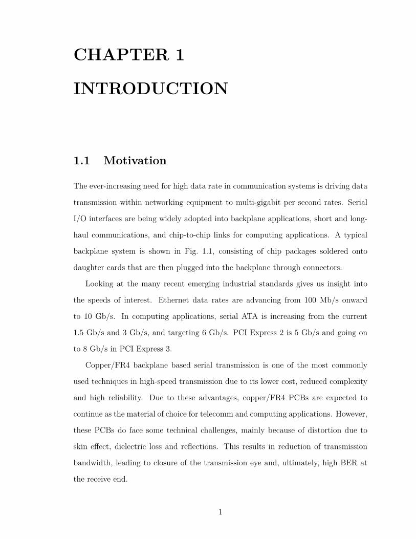
The ever-increasing need for high data rate in communication systems is driving data
transmission within networking equipment to multi-gigabit per second rates. Serial
I/O interfaces are being widely adopted into backplane applications, short and long-
haul communications, and chip-to-chip links for computing applications. A typical
backplane system is shown in Fig. 1.1, consisting of chip packages soldered onto
daughter cards that are then plugged into the backplane through connectors.
Looking at the many recent emerging industrial standards gives us insight into
the speeds of interest. Ethernet data rates are advancing from 100 Mb/s onward
to 10 Gb/s. In computing applications, serial ATA is increasing from the current
1.5 Gb/s and 3 Gb/s, and targeting 6 Gb/s. PCI Express 2 is 5 Gb/s and going on
to 8 Gb/s in PCI Express 3.
Copper/FR4 backplane based serial transmission is one of the most commonly
used techniques in high-speed transmission due to its lower cost, reduced complexity
and high reliability. Due to these advantages, copper/FR4 PCBs are expected to
continue as the material of choice for telecomm and computing applications. However,
these PCBs do face some technical challenges, mainly because of distortion due to
skin effect, dielectric loss and reflections. This results in reduction of transmission
bandwidth, leading to closure of the transmission eye and, ultimately, high BER at
the receive end.
1

Daughter Card Trace
Connector
Package
Backplane Trace
Figure 1.1: Backplane link diagram.
1.2 High Speed Data Links
A communication link typically consists of a transmitter, the communication channel,
and a receiver (Fig. 1.2). The transmitter takes the digital data and converts it
to analog waveforms on the channel. The channel is the communication medium
between the transmitter and the receiver, and can have physical realizations such as
free space for wireless communication, optical fibers for optical communication and
PCB traces, coaxial cables or twisted pair wires for off-chip electrical communication.
When a channel is implemented using electrical technologies, the implementation is
often referred to as an interconnect.
ChannelTransmitter Receiver
Figure 1.2: Communication link.
1.3 Challenges of Multi-Gigabit Backplane DataTransmission
The challenges of multi-gigabit data transmission can largely be divided into two
categories, the first being structural issues and the second being frequency dependent
2
loss due to material properties. One of the greatest structural challenges is overcoming
impedance mismatches due to connector-via transitions. Improved laminates and
optimized connector-via architectures can alleviate these issues, but as data rates
steadily rise, the frequency dependent loss of the channel which usually manifests as
low-pass nature becomes a serious threat to signal integrity.
Skin effect describes how high frequency currents tend to travel on the surface of
the conductor, rather than the whole cross section of the conductor. This reduces the
effective conductive area of the trace, increasing resistance which causes the signal
to be attenuated. As frequencies increase into the multi-gigabit per second rates,
dielectric loss emerges as the dominant factor in high frequency attenuation, since its
effect is proportional to frequency, whereas skin effect is proportional to the square
root of frequency. Dielectric loss can be defined as a ratio of conductivity to frequency,
known as loss tangent. Materials such as FR-4 with a high loss tangent will see a large
attenuation of signal at high frequency. The combined attenuation and dispersion due
to these effects causes the signal to spread over to adjacent signals. This is called
intersymbol interference (ISI).
From a circuit point of view, the limited bandwidth of the channel increases the
rise-time/fall-time of the signal, which causes the voltage level of a single bit to depend
on the bit pattern it resides in. The degradation of the signal due to ISI results in
two main issues on the receiver side: reduced voltage margin and timing errors due
to jitter in zero crossings. In order to reduce BER, transmitter pre-emphasis, receiver
equalization, or a combination of the two is generally used to compensate the channel.
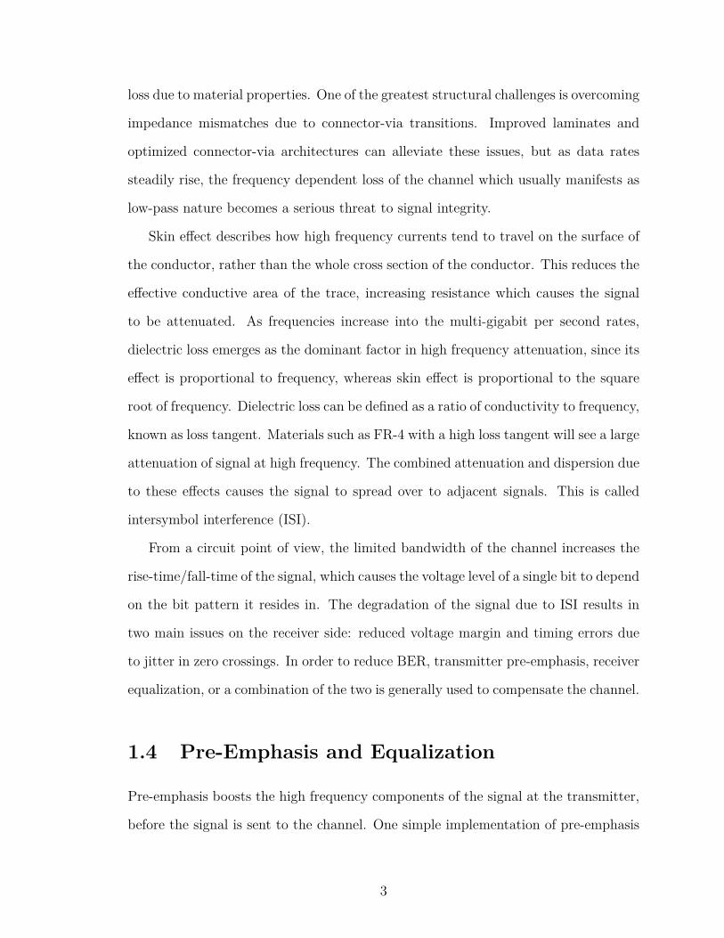
1.4 Pre-Emphasis and Equalization
Pre-emphasis boosts the high frequency components of the signal at the transmitter,
before the signal is sent to the channel. One simple implementation of pre-emphasis
3
is a 2-tap finite impulse response (FIR) filter, resulting in a boost of signal every time
there is a signal transition (Fig. 1.3).
Some of the disadvantages of pre-emphasis include higher power requirements
to boost the signal, aggravated crosstalk, and increased electromagnetic interference
(EMI) due to the overshoot and undershoot. Also, as the channel is usually not known
a priori, more focus is aimed at equalization design, while a simpler pre-emphasis
implementation is used.
D
X Z
a
Y
X
Y
Z
Figure 1.3: Simple pre-emphasis implementation.
Equalization is used at the receiver to flatten the channel frequency response
to overcome the high frequency signal loss during transmission. Receivers can be
implemented in discrete-time or continuous-time. Continuous-time receivers can be
designed using an analog equalizer, while discrete-time equalizers can be designed
using digital filters.
Several types of discrete-time designs can be considered. As introduced in the
literature [1], using a maximum-likelihood sequence estimation (MLSE) receiver is
optimum according to a probability of error criterion. However MLSE has a com-
plexity that grows exponentially with the length of the ISI channel time dispersion,
which makes implementation expensive. Other sub-optimum methods include using
a linear transversal equalizer (LE) or a decision feedback equalizer (DFE).
The linear transversal equalizer (LE), which can be viewed as being the same as a
FIR filter, is very versatile in that an infinite length LE can equalize any channelH(ω)
as long as H(ω) 6= 0, |ω| ≤ πT
. Also, it can be used to implement matched filtering
as well if the taps are spaced at Nyquist intervals instead of symbol intervals [2, 3].
4
One of the main disadvantages of using a common LE design is that the equalizer
usually has a high-pass characteristic due to the low-pass nature of the channel. This
can result in severe amplification of high frequency noise components, especially with
channels with spectral nulls.
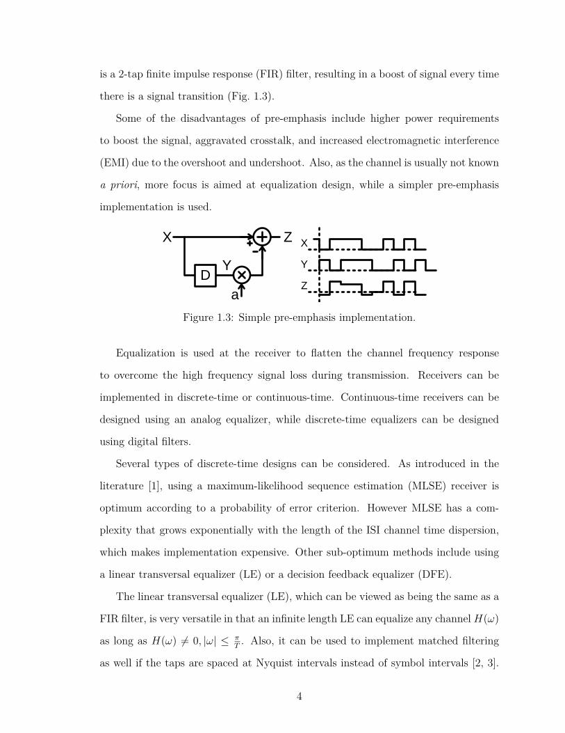
The decision feedback equalizer (DFE) is a non-linear filter which allows some of
the noise problems associated with linear equalizers to be overcome. By using a linear
combination of past decisions, the DFE compensates for the channel response while
eliminating noise amplification. While the DFE is vulnerable to ‘error propagation’
where an initial decision error will feed back and cause a sequence of errors, the system
will recover from the error events in relatively short order if the data is insured to be
random [4].
Figure 1.4 shows the operation of a DFE canceling postcursor ISI, in which the
pulse response of a channel is assumed to be a simple RC low-pass filter [5].
D
X Y
a1 D
D
D
a2
a3
a4
(a)
a1
a2 a3 a4
1
(b)
Figure 1.4: (a) Simple DFE system. (b) DFE removing postcursor ISI.
5
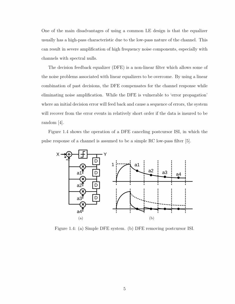
1.5 Receiver Design for AWGN ISI Channelsusing DFE
Figure 1.5 shows the optimum equalizer receiver design process for digital transmission
channels corrupted by AWGN and ISI [4, 6]. A matched filter is used for maximum
SNR before the sampler, and a noise whitening filter is selected so that the resulting
response is minimum phase. This creates a causal and stable output F (z), effectively
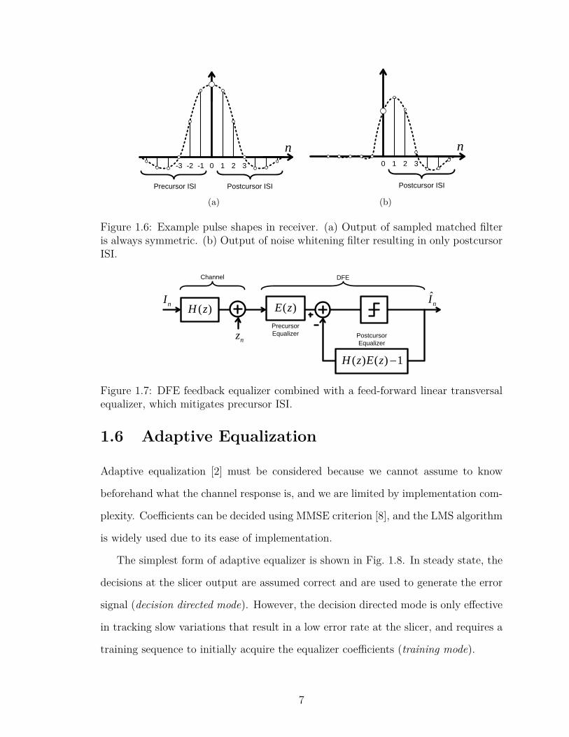
eliminating precursor ISI, as shown in Fig. 1.6. The matched filter, symbol-rate
sampler and noise whitening filter are collectively called the whitened matched filter
(WMF). As can be seen, the DFE front-end is equivalent to the WMF [7], which
ultimately operates as the precursor equalizer for a DFE (Fig. 1.7).
( )c t *( )h t( )g tnI
...10001001
( )h t
Transmitter
pulse shape
Channel freq
responseMatched filter
AWGN
( )z t
* 1
1
( )F z( )X z
Non-white
Gaussian Noise
nvNoise
whitening filter
nI...10001001
t kT
1
( )F z( )F z
AWGN
n Equalizer
Discrete-time model
of channel with ISI
( )r t
Received
Signal
Whitened-Matched Filtered
ISI channel model
AWGN ISI Channel
nI...10001001
Symbol-spaced
sampler
Figure 1.5: Optimum receiver design with equalizer.
6
n
0 1 2-1-2 3-3
0 1 2 3
n
Postcursor ISIPrecursor ISI
Postcursor ISI
(a)
n
0 1 2-1-2 3-3
0 1 2 3
n
Postcursor ISIPrecursor ISI
Postcursor ISI
(b)
Figure 1.6: Example pulse shapes in receiver. (a) Output of sampled matched filteris always symmetric. (b) Output of noise whitening filter resulting in only postcursorISI.
( )H z ( )E znI
Precursor
Equalizernz
Channel DFE
( ) ( ) 1H z E z
Postcursor
Equalizer
ˆnI
Figure 1.7: DFE feedback equalizer combined with a feed-forward linear transversalequalizer, which mitigates precursor ISI.
1.6 Adaptive Equalization
Adaptive equalization [2] must be considered because we cannot assume to know
beforehand what the channel response is, and we are limited by implementation com-
plexity. Coefficients can be decided using MMSE criterion [8], and the LMS algorithm
is widely used due to its ease of implementation.
The simplest form of adaptive equalizer is shown in Fig. 1.8. In steady state, the
decisions at the slicer output are assumed correct and are used to generate the error
signal (decision directed mode). However, the decision directed mode is only effective
in tracking slow variations that result in a low error rate at the slicer, and requires a
training sequence to initially acquire the equalizer coefficients (training mode).
7

Received
SignalReceive
Filter
Adaptive
Equalizer
Slicer
Training Signal
Sampler
Error Signal
Decisions
Training
mode
Decision
directed
mode
Figure 1.8: Adaptive receiver block diagram.
To avoid singularities from the zero of the channel transfer function inside the unit
circle, we can select an equalizer such that W (z)H(z) ∼= z−L, where the result is a
time-shifted version of the desired signal, as shown in Fig. 1.9. A more generalW (z) =
Y (z)/H(z) can also be used to reduce noise enhancement or to ease implementation,
in what is known as a partial-response signaling system [9].
( )H z ( )W z...10001001
Channel freq
response
Adaptive LMS
equalizer
( )n
Lz
( )I n
( ) ( )I n L d n
( )e n
Figure 1.9: Alternative training system.
1.7 Thesis Organization
This thesis documents all the effort devoted to design and improve upon a high-speed
serial link receiver. Chapter 2 describes the design of a continuous-time receiver
equalizer for use in 10 Gb/s data links. A discrete-time adaptive DFE receiver is
simulated using ADS and measured channel S-parameters in Chapter 3.
8
CHAPTER 2
CONTINUOUS-TIMEEQUALIZER DESIGN
2.1 Methodology
Compared with discrete-time equalizers, continuous-time equalizers have some attrac-
tive properties in terms of noise, jitter and potential power dissipation. The use of
passive networks is also gaining attention due to the low power and smaller size of
implementation. In this chapter, an analog equalizer is designed for use in a 10 Gb/s
data receiver.
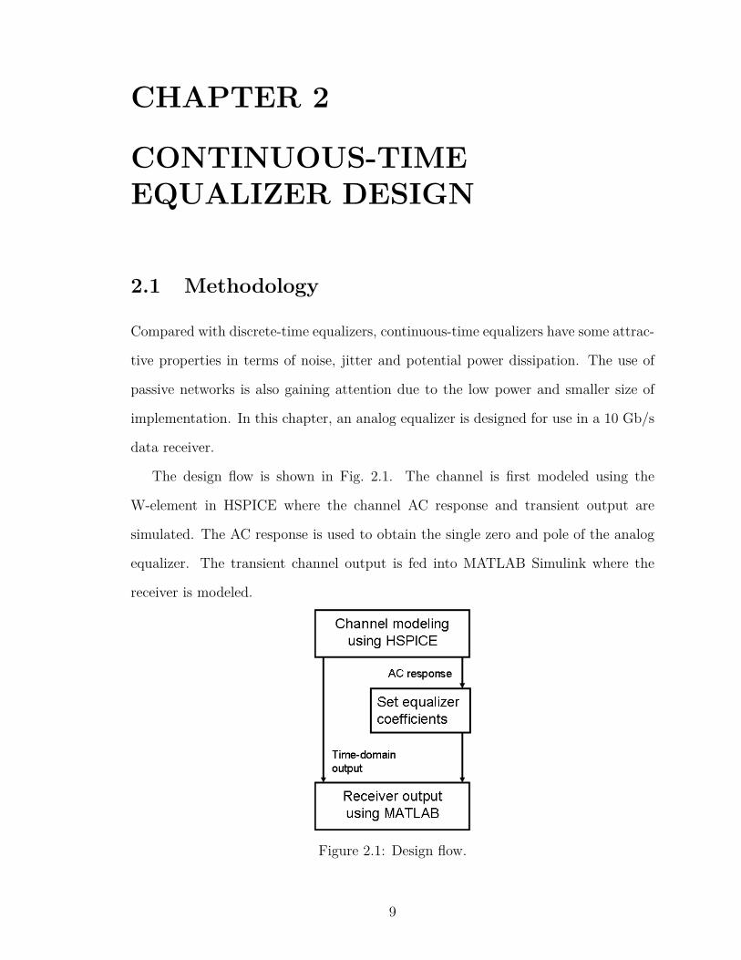
The design flow is shown in Fig. 2.1. The channel is first modeled using the
W-element in HSPICE where the channel AC response and transient output are
simulated. The AC response is used to obtain the single zero and pole of the analog
equalizer. The transient channel output is fed into MATLAB Simulink where the
receiver is modeled.
Figure 2.1: Design flow.
9
2.2 Channel Model
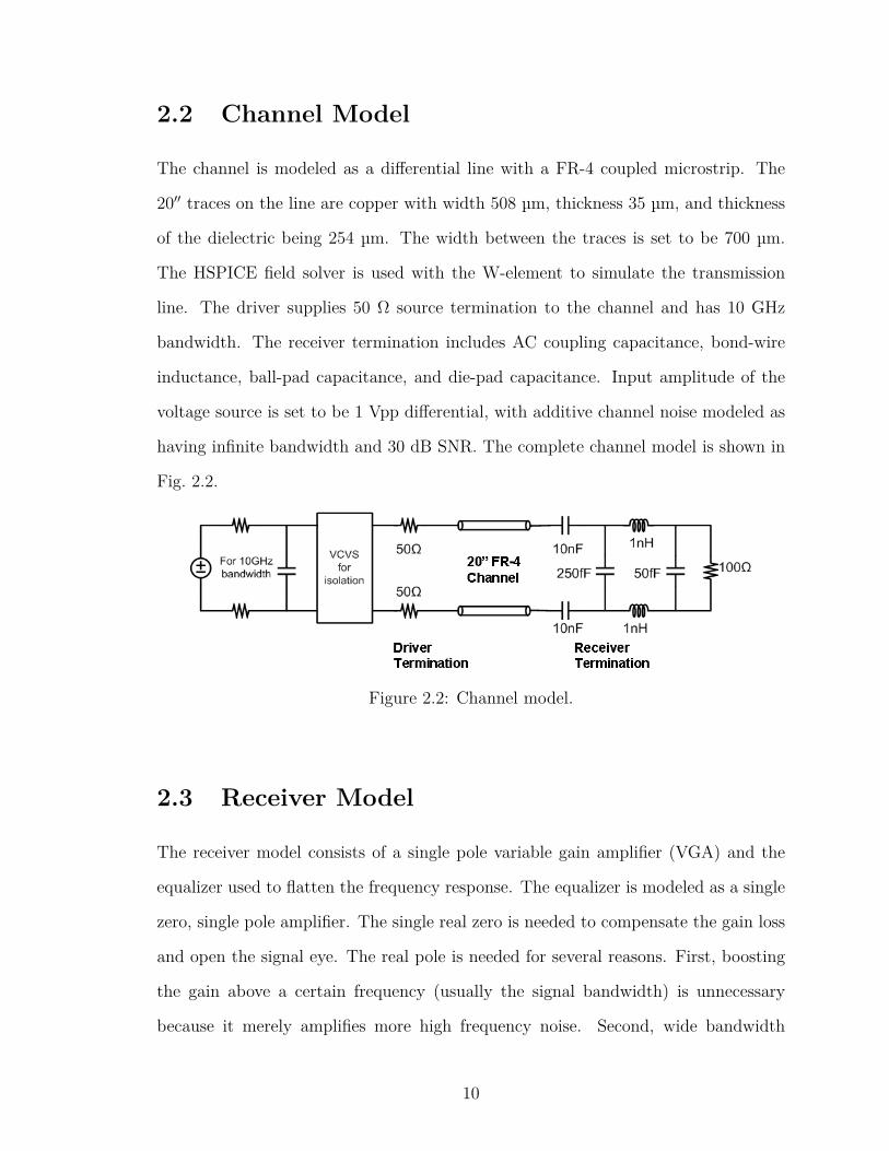
The channel is modeled as a differential line with a FR-4 coupled microstrip. The
20′′ traces on the line are copper with width 508 µm, thickness 35 µm, and thickness
of the dielectric being 254 µm. The width between the traces is set to be 700 µm.
The HSPICE field solver is used with the W-element to simulate the transmission
line. The driver supplies 50 W source termination to the channel and has 10 GHz
bandwidth. The receiver termination includes AC coupling capacitance, bond-wire
inductance, ball-pad capacitance, and die-pad capacitance. Input amplitude of the
voltage source is set to be 1 Vpp differential, with additive channel noise modeled as
having infinite bandwidth and 30 dB SNR. The complete channel model is shown in
Fig. 2.2.
Figure 2.2: Channel model.
2.3 Receiver Model
The receiver model consists of a single pole variable gain amplifier (VGA) and the
equalizer used to flatten the frequency response. The equalizer is modeled as a single
zero, single pole amplifier. The single real zero is needed to compensate the gain loss
and open the signal eye. The real pole is needed for several reasons. First, boosting
the gain above a certain frequency (usually the signal bandwidth) is unnecessary
because it merely amplifies more high frequency noise. Second, wide bandwidth
10
causes signal peaking in the middle of the eye, generating large jitter at zero crossing
points of the data signal. Signal peaking in the middle of the eye also decreases the
voltage margin at the middle of the eye, which increases BER. Finally, signal peaking
increases crosstalk between signal lines.
Thus the real pole is needed to limit the bandwidth. The pole location determines
the amount of boosting and the frequency range due to the zero. If the signal loss
is low, the zero and the pole can be close together. But, if the loss is high, the zero
and the pole should be separated further to get sufficient boosting. It is desirable to
have the zero and pole as close as possible to avoid adding excessive non-linear phase
response, for a symmetrical eye.
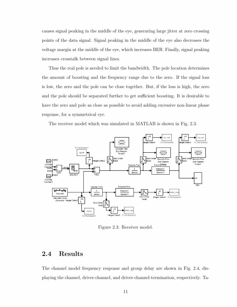
The receiver model which was simulated in MATLAB is shown in Fig. 2.3.
Figure 2.3: Receiver model.
2.4 Results
The channel model frequency response and group delay are shown in Fig. 2.4, dis-
playing the channel, driver-channel, and driver-channel-termination, respectively. Ta-
11
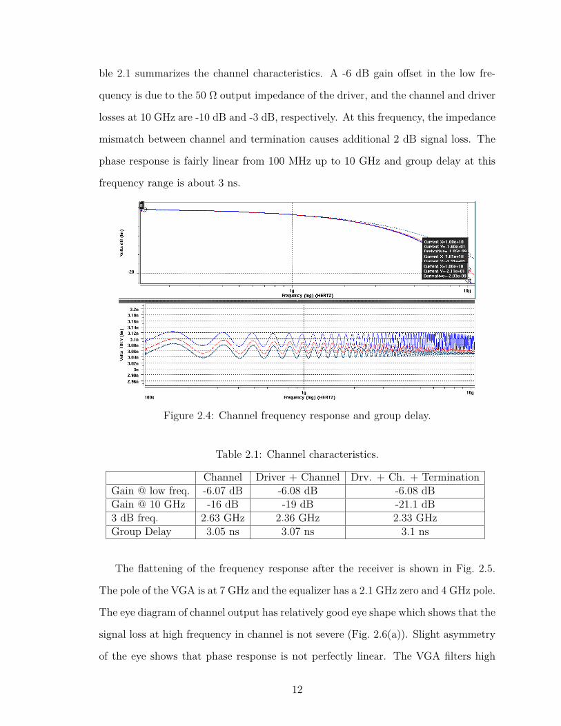
ble 2.1 summarizes the channel characteristics. A -6 dB gain offset in the low fre-
quency is due to the 50 W output impedance of the driver, and the channel and driver
losses at 10 GHz are -10 dB and -3 dB, respectively. At this frequency, the impedance
mismatch between channel and termination causes additional 2 dB signal loss. The
phase response is fairly linear from 100 MHz up to 10 GHz and group delay at this
frequency range is about 3 ns.
Figure 2.4: Channel frequency response and group delay.
Table 2.1: Channel characteristics.
Channel Driver + Channel Drv. + Ch. + TerminationGain @ low freq. -6.07 dB -6.08 dB -6.08 dBGain @ 10 GHz -16 dB -19 dB -21.1 dB3 dB freq. 2.63 GHz 2.36 GHz 2.33 GHzGroup Delay 3.05 ns 3.07 ns 3.1 ns
The flattening of the frequency response after the receiver is shown in Fig. 2.5.
The pole of the VGA is at 7 GHz and the equalizer has a 2.1 GHz zero and 4 GHz pole.
The eye diagram of channel output has relatively good eye shape which shows that the
signal loss at high frequency in channel is not severe (Fig. 2.6(a)). Slight asymmetry
of the eye shows that phase response is not perfectly linear. The VGA filters high
12
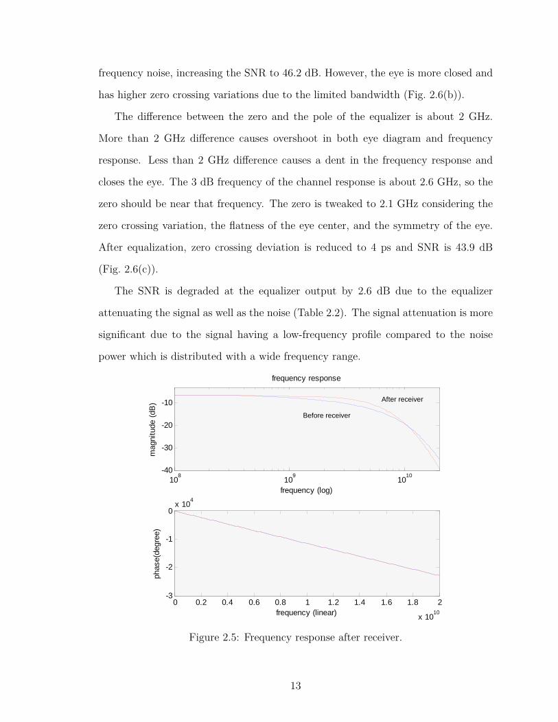
frequency noise, increasing the SNR to 46.2 dB. However, the eye is more closed and
has higher zero crossing variations due to the limited bandwidth (Fig. 2.6(b)).
The difference between the zero and the pole of the equalizer is about 2 GHz.
More than 2 GHz difference causes overshoot in both eye diagram and frequency
response. Less than 2 GHz difference causes a dent in the frequency response and
closes the eye. The 3 dB frequency of the channel response is about 2.6 GHz, so the
zero should be near that frequency. The zero is tweaked to 2.1 GHz considering the
zero crossing variation, the flatness of the eye center, and the symmetry of the eye.
After equalization, zero crossing deviation is reduced to 4 ps and SNR is 43.9 dB
(Fig. 2.6(c)).
The SNR is degraded at the equalizer output by 2.6 dB due to the equalizer
attenuating the signal as well as the noise (Table 2.2). The signal attenuation is more
significant due to the signal having a low-frequency profile compared to the noise
power which is distributed with a wide frequency range.
5
In addition to the flatness of the frequency response, the phase response should be linear to get the symmetric eye shape. In that sense, the zero and the pole should be close because the farther the zero and the pole are, the more nonlinear phase response is added to the channel phase response.
Another real pole is inserted in the variable gain amplifier (VGA). The channel noise is modeled after the channel with infinite bandwidth. The pole of VGA will attenuate the channel noise.
B. Specifications
• 20dB gain range linear VGA o Linearity : 25dB IMD worst case (250mVpp test tone at 5G and 6GHz)
• high frequency boosting filter (analog equalizer) for skin loss compensation o single real zero and single real pole
• <15ps spread in zero crossing after equalization • Zero should be tunable.
C. AFE modeling
• VGA is modeled with ideal amplifier with a real pole and infinite linearity. • Analog equalizer is modeled with s-domain transfer function in MATLAB, and
filter using ideal Rs and Cs in Verilog-A.
D. Simulation Results
The eye diagram of channel output has relatively good eye shape which shows the signal loss at high frequency in channel and termination is not severe. ZFE is a good choice as an equalizer because SNR of channel output is high, 30dB. A little asymmetry of eye tells that phase response is not perfectly linear. High frequency noise is filtered by the low-pass characteristic of VGA, thus SNR of VGA output is increased to 46dB. However, eye is closed more and zero crossing variation is higher because of the limited bandwidth.
108 109 1010-40
-30
-20
-10
frequency response
mag
nitu
de (d
B)
frequency (log)
0 0.2 0.4 0.6 0.8 1 1.2 1.4 1.6 1.8 2
x 1010
-3
-2
-1
0x 104
phas
e(de
gree
)
frequency (linear) Figure 5. frequency response after AFE.
Before receiver
After receiver
Figure 2.5: Frequency response after receiver.
13
6
SNR : 30.2dB SNR : 46.2dB zero crossing variation : 10ps zero crossing variation : 15ps
(a) channel output. (b) VGA output : 7GHz real pole.
zero : 2.1GHz, pole : 4GHz
SNR : 43.9dB zero crossing variation : 4ps
(c) eye diagram – equalizer output.
Figure 6. Eye Diagram.
The zero and pole of the analog equalizer are 2.1GHz and 4GHz, respectively, thus, the distance between the zero and the pole is about 2GHz. More than 2GHz distance causes overshoot in both eye diagram and frequency response. Less than 2GHz distance causes dent in the frequency response and closes the eye. 3dB frequency of channel response is about 2.6GHz, so, the zero should be around that frequency. After lost of simulation, the zero is set to 2.1GHz considering the zero crossing variation, the flatness of the eye center, and the symmetry of the eye. Although VGA and equalizer have the nonlinear phase response, the effect is not significant because the maximum phase deviation of equalizer is less than 20° (this is because the zero and pole of equalizer is close.) and the phase deviation of VGA at below 7GHz is 45° (the pole of VGA is 7GHz). Furthermore , the phase deviations of VGA and equalizer are opposite each other. After equalization, zero crossing deviation is only 4ps and SNR is 43.9dB.
Fig. 7 shows the discrete-time frequency response with 10GS/s. If the frequency response is flat in the entire frequency (DC~10GHz) the signal does not have ISI at the sampling points. Before the equalization, the frequency response has the maximum 2dB difference in magnitude. After equalization, the frequency response is much flatter especially above 1GHz as expected in zero-forcing equalizer.
(a) Channel output
6
SNR : 30.2dB SNR : 46.2dB zero crossing variation : 10ps zero crossing variation : 15ps
(a) channel output. (b) VGA output : 7GHz real pole.
zero : 2.1GHz, pole : 4GHz
SNR : 43.9dB zero crossing variation : 4ps
(c) eye diagram – equalizer output.
Figure 6. Eye Diagram.
The zero and pole of the analog equalizer are 2.1GHz and 4GHz, respectively, thus, the distance between the zero and the pole is about 2GHz. More than 2GHz distance causes overshoot in both eye diagram and frequency response. Less than 2GHz distance causes dent in the frequency response and closes the eye. 3dB frequency of channel response is about 2.6GHz, so, the zero should be around that frequency. After lost of simulation, the zero is set to 2.1GHz considering the zero crossing variation, the flatness of the eye center, and the symmetry of the eye. Although VGA and equalizer have the nonlinear phase response, the effect is not significant because the maximum phase deviation of equalizer is less than 20° (this is because the zero and pole of equalizer is close.) and the phase deviation of VGA at below 7GHz is 45° (the pole of VGA is 7GHz). Furthermore , the phase deviations of VGA and equalizer are opposite each other. After equalization, zero crossing deviation is only 4ps and SNR is 43.9dB.
Fig. 7 shows the discrete-time frequency response with 10GS/s. If the frequency response is flat in the entire frequency (DC~10GHz) the signal does not have ISI at the sampling points. Before the equalization, the frequency response has the maximum 2dB difference in magnitude. After equalization, the frequency response is much flatter especially above 1GHz as expected in zero-forcing equalizer.
(b) VGA output
6
SNR : 30.2dB SNR : 46.2dB zero crossing variation : 10ps zero crossing variation : 15ps
(a) channel output. (b) VGA output : 7GHz real pole.
zero : 2.1GHz, pole : 4GHz
SNR : 43.9dB zero crossing variation : 4ps
(c) eye diagram – equalizer output.
Figure 6. Eye Diagram.
The zero and pole of the analog equalizer are 2.1GHz and 4GHz, respectively, thus, the distance between the zero and the pole is about 2GHz. More than 2GHz distance causes overshoot in both eye diagram and frequency response. Less than 2GHz distance causes dent in the frequency response and closes the eye. 3dB frequency of channel response is about 2.6GHz, so, the zero should be around that frequency. After lost of simulation, the zero is set to 2.1GHz considering the zero crossing variation, the flatness of the eye center, and the symmetry of the eye. Although VGA and equalizer have the nonlinear phase response, the effect is not significant because the maximum phase deviation of equalizer is less than 20° (this is because the zero and pole of equalizer is close.) and the phase deviation of VGA at below 7GHz is 45° (the pole of VGA is 7GHz). Furthermore , the phase deviations of VGA and equalizer are opposite each other. After equalization, zero crossing deviation is only 4ps and SNR is 43.9dB.
Fig. 7 shows the discrete-time frequency response with 10GS/s. If the frequency response is flat in the entire frequency (DC~10GHz) the signal does not have ISI at the sampling points. Before the equalization, the frequency response has the maximum 2dB difference in magnitude. After equalization, the frequency response is much flatter especially above 1GHz as expected in zero-forcing equalizer.
(c) Equalizer output
Figure 2.6: Eye diagrams of receiver.
Table 2.2: Receiver output
Channel Output VGA Output Equalizer OutputSignal Power Sum 0.0358 W·Hz 0.0312 W·Hz 0.049 W·HzNoise Power Sum 3.44× 10⁻⁵ W·Hz 7.46× 10⁻⁷ W·Hz 2.02× 10⁻⁶ W·HzSNR 30.2 dB 46.2 dB 43.9 dBZero Crossing Variation 10 ps 15 ps 4 ps
14

CHAPTER 3
DISCRETE-TIME ADAPTIVEEQUALIZER DESIGN
3.1 Methodology
In many cases, the channel of interest is unknown or has characteristics that vary
over time and temperature. This is very common in backplanes where by design,
daughter cards are meant to be able to be installed or uninstalled according to the
user’s needs. In this case an adaptive method of updating the coefficients of the
equalizers is most desirable. Given the measured S-parameters from a backplane, we
design and simulate a discrete-time adaptive DFE to equalize a 10 Gb/s data link.
Using the Signal Integrity Workshop DesignGuide in Advanced Design System
(ADS), an adaptive DFE is modeled and simulated. The LMS algorithm [1, 9] is
used to adaptively find the equalizer coefficients for both precursor and postcursor
parts of the receiver. Unlike the system described in the previous chapter, this system
is simulated in discrete-time with a global clock, and so zero crossings are a non-issue
in this case.
The backplane of interest is a 1 m Nelco 4000 13-SI board having 2.5′′ traces
on each daughter card. The measured 4-port S-parameters of the backplane were
obtained from the IEEE 802.3ap Backplane Ethernet Task Force [10] (Fig. 3.1). The
frequency response of the channel is shown in Fig. 3.2.
15
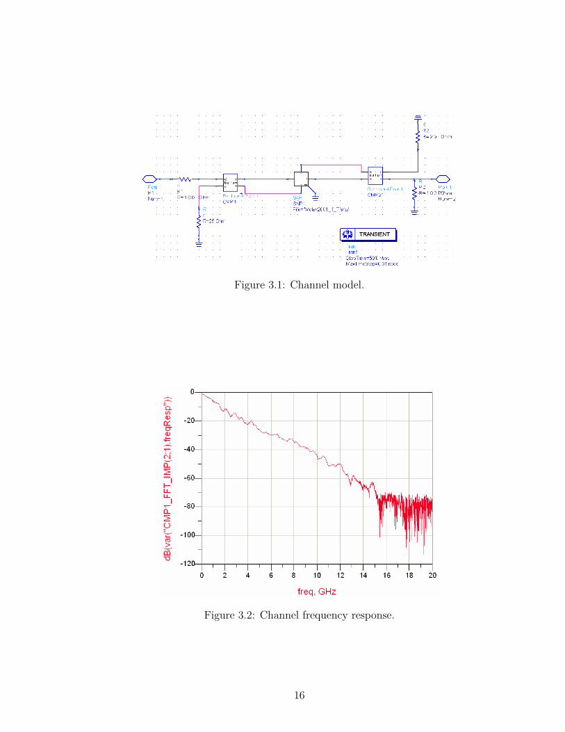
Figure 3.1: Channel model.
Figure 3.2: Channel frequency response.
16

3.2 Receiver Design
The receiver is modeled as a 7-tap precursor and 7-tap postcursor symbol-spaced
equalizer (Fig. 3.3). Transmit bits are generated using a pseudo-random bit sequence.
An initial training period using the correct transmitted data is required to converge
the DFE before the receiver is able to begin coefficient tracking, where the slicer
decisions are used instead.
Figure 3.3: System model.
3.3 Results
The LMS algorithm is seen to be successfully converged and the channel equalized.
As symbol-spaced sampling is used, an open discrete-time eye diagram is obtained
using the data at the input of the decision slicer (Fig. 3.4).
17
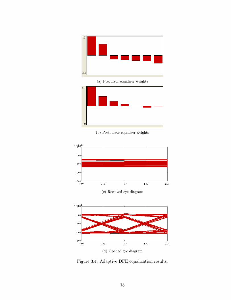
(a) Precursor equalizer weights
(b) Postcursor equalizer weights
(c) Received eye diagram
(d) Opened eye diagram
Figure 3.4: Adaptive DFE equalization results.
18
CHAPTER 4
CONCLUSION
We have presented two different equalizer architectures suitable for 10 Gb/s serial
data links. Design trade-offs in both transmit-side and receive-side equalizers were
described. A continuous-time equalizer was designed to equalize a channel with known
characteristics. An adaptive DFE for use in unknown or time-varying channels was
also presented. Future work could be extended to parallel architectures, and the use
of pre-computation or pipelining architectures such as unfolding could be included
for higher performance.
19

REFERENCES
[1] J. Proakis and D. Manolakis, Digital Signal Processing: Principles, Algorithms,and Applications. Upper Saddle River, NJ: Prentice-Hall, Inc., 1996.
[2] R. Lucky, J. Salz, and E. Weldon, Principles of Data Communication. NewYork, NY: McGraw-Hill, 1968.
[3] M. DiToro, “A new method of high-speed adaptive serial communication throughany time-variable and dispersive transmission medium,” in 1st IEEE AnnualCommunication Convention, 1965, pp. 763–767.
[4] J. Barry, E. Lee, and D. Messerschmitt, Digital Communication. Norwell, MA:Kluwer Academic Publishers, 2004.
[5] B. Song and D. Soo, “NRZ timing recovery technique for band-limited channels,”IEEE Journal of Solid-State Circuits, vol. 32, no. 4, pp. 514–520, 1997.
[6] J. Proakis, Digital Communications. New York, NY: McGraw Hill InternationalEditions, 2001.
[7] R. Price, “Nonlinearly feedback-equalized PAM vs. capacity,” in Proceedings ofIEEE International Conference on Communications, Philadephia, PA, 1972, pp.22.12–22.17.
[8] J. Cioffi, G. Eyuboglu, and M. Forney, “MMSE decision-feedback equalizers andcoding. Part I. Equalization results,” IEEE Transactions on Communications,vol. 43, no. 10, pp. 2582–2594, 1995.
[9] A. Poularikas and Z. Ramadan, Adaptive Filtering Primer with MATLAB. BocaRaton, FL: CRC Press, 2006.
[10] G. Oganessyan, “IEEE P802.3ap task force channel model material,”2006. [Online]. Available: http://grouper.ieee.org/groups/802/3/ap/public/channel model/index.html
20