high-throughput computational design of organic-inorganic
TRANSCRIPT

High-throughput Computational Design of Organic-inorganic Hybrid Halide Semiconductors Beyond Perovskites for
Optoelectronics
Journal: Energy & Environmental Science
Manuscript ID EE-ART-04-2019-001371.R1
Article Type: Paper
Date Submitted by the Author: 15-May-2019
Complete List of Authors: Li, Yuheng; University of California San Diego, NanoEngineeringYang, Kesong; University of California San Diego, NanoEngineering
Energy & Environmental Science

Journal Name
High-throughput Computational Design of Organic-inorganic Hybrid Halide Semiconductors beyond Per-ovskites for Optoelectronics†
Yuheng Lia and Kesong Yanga,b,c
Organic-inorganic lead halide perovskites show great promise in optoelectronic applications suchas light-emitting diodes and solar energy conversion. However, the poor stability and toxicityof lead halide perovskites severely limit their large-scale applications. Here we show a high-throughput design of lead-free hybrid halide semiconductors with robust materials stability and de-sired material properties beyond perovskites. On the basis of 24 prototype structures that includeperovskite and non-perovskite structures and several typical organic cations, a comprehensivequantum materials repository that contains 4507 hypothetical hybrid compounds was built usinglarge-scale first-principles calculations. After a high-throughput screening of this repository, wehave rapidly identified 23 candidates for light-emitting diodes and 13 candidates for solar energyconversion. Our work demonstrates a new avenue to design novel organic-inorganic functionalmaterials by exploring a great variety of prototype structures.
1 IntroductionOrganic-inorganic hybrid lead halide perovskites with a prototyp-ical formula of MAPbI3 (MA=CH3NH3) are one emerging classof semiconductor materials with promising optoelectronic ap-plications including solar energy conversion and light-emittingdiodes.1,2 This is mainly attributed to their excellent materialsproperties such as tunable band gaps3, high charge carrier mo-bility4, defect tolerance5, and low-temperature solution process-ability6. In spite of their promising optoelectronic applications,particularly for solar energy conversion, the hybrid lead halideperovskites are facing two major challenges including poor sta-bility and presence of toxic lead, which limits their large-scaleapplications.7,8 To overcome these challenges, one solution is tosearch for novel hybrid materials with potentially superior prop-erties beyond or like that of lead-based hybrid halide perovskites.
Some prior experimental and computational efforts both havebeen made to explore alternatives to lead halide perovskites.There are two major classes of candidates that are being exten-sively studied. One class of candidates are Ge- and Sn-basedhalide perovskites with various organic cations, but these ma-terials usually have even lower stability than lead halide per-
aDepartment of NanoEngineering, University of California San Diego, 9500 GilmanDrive, Mail Code 0448, La Jolla, California 92093-0448, USA. bProgram of Materi-als Science and Engineering, University of California San Diego, La Jolla, California92093-0418, USA. cCenter for Memory and Recording Research, University of Califor-nia San Diego, La Jolla, California 92093-0401, USA. Fax: +1-858-534-9553; Tel:+1-858-534-2514; E-mail: [email protected]
ovskites.9 To enhance stability of Sn-based perovskites, some ex-perimental approaches such as the fabrication of low-dimensionalstructures10 and the encapsulation of device11 have been pro-posed. In addition to Ge and Sn, Si mixed with other cationssuch as Ca/Si and Zn/Si with different ratios were also tried.12
The other class of candidates are called double perovskites witha chemical formula A2BB'X6 (A=Cs or organic cations; X=Cl,Br, or I), which can be regarded as derivatives of single per-ovskite MAPbX3 but with Pb replaced by two different metalcations (B=B+; B'=B3+).13–19 Early experimental demonstra-tion of double perovskites for optoelectronics include Cs-basedinorganic double perovskites with Ag-Bi composition13–15 andthe MA-based hybrid double perovskite with K-Bi composition.16
Nevertheless, most double perovskites that are predicted to havegood electronic properties often suffer from instability issues suchas phase separation or redox decomposition, e.g., Cs2InBiCl6 andCs2InSbCl6,20 while double perovskites that can be synthesizedusually show large indirect band gaps.13–16 Despite this, exten-sive research efforts are being made to search for novel doubleperovskites with desired electronic properties and high stability,such as using high-throughput materials design approach,17–19
towards lead-free perovskite optoelectronics.21–23
Notably, these prior efforts primarily focused on the single per-ovskite structure with a stoichiometry of 1:1:3 or on the doubleperovskite with a stoichiometry of 2:1:1:6. Besides perovskitestructures, there exist in principles other organic-inorganic hybridternary metal halide compounds with appropriate metal elementsand the stoichiometry of component elements that are more sta-
Journal Name, [year], [vol.],1–11 | 1
Page 1 of 12 Energy & Environmental Science

ble and even show better optoelectronic properties than the typi-cal perovskite structures.24 As a proof of concept, Sb-based hy-brid ternary compound, (MA)3Sb2ClxI9−x, has been prepared,and the solar cell based on this material reached a power con-version efficiency over 2%;25 the ternary silver bismuth iodidesshowed tunable optoelectronic properties upon sulfide modifica-tion for photovoltaics.26 Therefore, it is worthwhile to explorenon-perovskite ternary structures for searching for alternatives tolead halide perovskites.
In this work, we have carried out a high-throughput computa-tional design of novel lead-free organic-inorganic ternary halidesemiconductors for optoelectronic applications using large-scalefirst-principles electronic structure calculations and have success-fully identified 13 candidates for photovoltaic applications and 23candidates for light-emitting applications. The chemical formu-las of selected candidates include A2BX4, A3B2X9, and A2BX6, inwhich A = MA, FA, or AD, and X=Cl, Br, or I. All these candidateshave robust materials stability, appropriate band gaps, effectivemasses, and exciton binding energies for the optoelectronic ap-plications.
2 Methods
The high-throughput first-principles calculations were performedusing the automatic framework AFLOW27 based on the ViennaAb-initio Simulation Package (VASP).28 The projector augmentedwave potentials, and the generalized gradient approximation(GGA) of the exchange-correlation functional as parameterizedby Perdew, Burek, and Ernzerholf (PBE) are used in the DFT cal-culations.29 To properly describe the long-range dispersion inter-actions between the organic molecules in the hybrid materials,two types of van der Waals (vdW) functionals including DFT-D330 and optB86b31 were carefully assessed for the prototypecompound MASnBr3, along with the standard PBE functional. Asshown in Table S1 of Supporting Information, our test calcula-tions suggest that both vdW functionals give more accurate equi-librium lattice parameters than the PBE functional while the DFT-D3 method shows a better match with the experimental valuethan the optB86b and thus is used in our calculations. Structuresare fully relaxed with a convergence tolerance of 0.01 meV/atom.k-points grid of 0.05 Å−1 were automatically set for relaxationof different structures. Accurate charge densities and density ofstates are obtained in static calculations with a denser grid of 0.04Å−1. Other computational settings such as cutoff energy are man-aged by the AFLOW code that also generates appropriate entriesfor the structural relaxation, static calculations, and the electronicband structure calculations sequentially and automatically.27 Thehybrid DFT calculations within Heyd-Scuseria-Ernzerhof (HSE)formalism with 25% Hartree-Fock (HF) exchange are employedto predict accurate band gaps for the candidate compounds.32,33
The parameter of 25% HF mixing constant was derived from per-turbation theory,32,33 which can generally yield close band gapsto the experiment and is appropriate for a large number and va-riety of hypothetical compounds.17,18
Table 1 Structural properties of the CsxByXz compounds used to extractprototype structures. Original inorganic compound, space group, ICSDnumber, and Pearson symbol. All the prototype structures are availablein the AFLOWLIB and/or Materials Project.
B+n Stoichi- Original Space ICSD Pearsonometry Compound Group Number Symbol
B+1 1:1:2Cs4Ag4Br8 Cmcm 150301 oS16Cs2Ag2Cl4 P4/nmm 150300 tP8
1:2:3 Cs4Cu8Br12 Cmcm 49613 oS24
B+2
1:1:3
Cs1Sn1Br3 Pm3m 4071 cP5Cs1Ge1Br3 R3m 80317 hR5Cs3Mn3Cl9 R3m 2555 hR15Cs4Ag4Cl12 I4/mmm 66067 tI20Cs2Cd2Br6 P63mc 281176 hP10Cs2Dy2Br6 P4/mbm 300285 tP10Cs4Cr4I12 Pbcn 23383 oP20Cs4Sn4I12 P21/m 14070 mP20Cs4Cr4Cl12 C2/m 41802 mS20Cs4Pb4I12 Pnma 161480 oP20'
2:1:4
Cs4Cd2Cl8 I4/mmm 16576 tI14Cs8Pd4Cl16 Cmmm 95812 oS28Cs4Hg2I8 P21/m 63110 mP14Cs8Zn4Br16 Pnma 69139 oP28
2:3:8 Cs4Hg6I16 Cm 4074 mS261:2:5 Cs2Hg4Br10 P21/m 200751 mP16
B+3 3:2:9Cs3Bi2Br9 P3m1 1142 hP14Cs6Mo4Br18 P63/mmc 26213 hP28
B+4 2:1:6Cs4Pd2I12 I4/mmm 280189 tI18Cs8Pt4Br24 Fm3m 77381 cF36Cs2CeCl6 P3m1 14339 hP9
3 Results3.1 Building RepositoryAs the first step, we built a quantum materials repository thatcontains hybrid halide perovskites and perovskite derivatives. Todo this, we began by identifying all possible prototype structuresbased on existing ternary metal halide compounds with a for-mula of CsxByXz from the online quantum materials databasesAFLOWLIB34 and Materials Project.35 The reason for selectingCs-contained compounds is as follows. The Cs cation has a largeionic radius that is comparable with that of the organic cationssuch as MA, and thus it can be readily substituted by organiccations to form organic-inorganic hybrid compounds. Note thatone chemical formula may correspond to different crystal struc-tures, and only the most stable one was selected as a prototypestructure. As shown in Fig. S1 of the Supporting Information, atotal number of 24 unique prototype structures were identified.Their complete structural information is listed in Table 1, includ-ing space group, ICSD number, and Pearson symbol. The uniquePearson symbol is used to denote these prototype structures. Forexample, the structure generated from the compound CsSnBr3
with a space group of Pm3m and an ICSD number of 4071 (iden-tifed as CsSnBr3_ICSD_4071 in AFLOWLIB) is denoted using itsPearson symbol of cP5. The prototype structures cP5 and tI20(tP10) are the cubic and tetragonal perovskites, respectively, and
2 | 1–11Journal Name, [year], [vol.],
Page 2 of 12Energy & Environmental Science

Quantum Materials Repository
Prototype Structures
…#001 #002 #003 #023 #024
h𝒗
h𝒗
𝚫q
𝚫Hfdiff
0.0150
Electronic Structure Stability Other Descriptors
𝚫Hd stability w.r.t. decomposition 𝐸$ = 𝜇∗𝑅*𝑚,𝜀./Photovoltaic
Light-Emitting
𝚫Hfdiff ≤ 0.015 eV/atom
competing phases
𝚫Hd ≥ 0.03 eV/f.u.h𝒗
23 candidates
13candidates4507 hypothetical compounds
MA AD FA EA DMA
A-B-X Compositions
B 65 BI/BII/BIII/BIV I/Br/ClX
~800 candidates
not synthesizablesynthesizable
~200 candidates
AxByXz → AX + BXn,AxByXz → AX + BXm + X2, etc.
(𝜀. = 𝜀1)
BuildingRepository
High-ThroughputDFT Calculations
ScreeningProcess
FinalCandidates
A
Eg: 1.65 – 3 eVme*, mh* ≤ 1.5m0
Eg: 0.8 – 2.2 eVme*, mh* ≤ 1.5m0 AIMD thermal stability at 300 K
Exciton Binding Energy
Remove compounds with toxic elements (As, Cd, Hg, Tl, Pb)
Non-Toxicity
Fig. 1 Schematic diagram of the high-throughput screening process. A total number of 4507 compounds (AxByXz, A = MA/FA/AD/EA/DMA, X = I/Br/Cl)were generated from 65 kinds of B-site elements in 24 different crystal structures. Compounds with direct band gaps in the visible spectrum rangeare kept for light-emitting materials, and compounds with band gaps in 0.8-2.2 eV are kept for solar-cell materials. Compounds with effective massesgreater than 1.5m0 are excluded. Compounds with a formation enthalpy higher than its most energetically favorable competing phase by a value greaterthan 0.015 eV/atom are excluded. Compounds containing toxic B-site elements are also excluded. Compounds that cannot maintain structural integrityat room temperature are excluded. The selected candidates are all stable with respect to decomposition by at least 0.03 eV/formula unit. Compoundswith exciton binding energy greater than 130 meV are excluded for solar-cell materials. 23 candidates for light-emitting materials and 13 candidates forsolar-cell materials were selected.
the others are perovskite derivatives. Note that two prototypes,CsCrI3_ICSD_23383 and CsPbI3_ICSD_161480, share the samePearson symbol of oP20, and to distinguish them, we denote theformer with oP20, and the later with oP20'.
After identifying the structure prototypes, we next generate hy-pothetical compounds by placing various elements in the AxByXz
formula. At A site, we put relatively small organic cations, includ-ing MA (CH3NH3), FA (CH(NH2)2), AD ((CH2)2NH2)36, DMA(NH2(CH3)2), and EA (C2H5NH3). At B site, we select elementswith different valence states according to the different stoichiom-etry of AxByXz. As shown in Table 1, there are three structure pro-totypes for B+, 16 prototypes for B2+, two prototypes for B3+, andthree prototypes for B4+. B+-based prototypes have two differentstoichiometries (A:B:X=1:1:2 and 1:2:3); B2+-based prototypeshave four different stoichiometries (A:B:X=1:1:3, 2:1:4, 2:3:8,and 1:2:5); B3+-based prototypes only have one stoichiometry(A:B:X=3:2:9); and B4+-based prototypes also only have one sto-ichiometry (A:B:X=2:1:6). A total number of 65 possible B-siteelements with common valence states from +1 to +4 were placedin the corresponding prototypes. The X site is occupied by I, Br,or Cl ions. With the three sites combined in the 24 prototypes,a total number of 4507 hypothetical compounds were generated.The electronic structure of all the compounds is computed in ahigh-throughput fashion.
3.2 Screening Process
In terms of optoelectronic applications like solar cells and lightemitters, there are several common descriptors often used forhigh-throughput screening of target materials. These descriptors
include band gap, charge carrier effective masses, and decom-position enthalpy. Our detailed criteria for each descriptor arediscussed as below:
(i) Band gap (Eg). We obtained band gaps using DFT calcu-lations with two different types of functionals: One is calculatedwith the standard GGA functional (EGGA
g ), and the other is cal-culated with the hybrid functionals (EHSE
g )32. This is becausethe GGA functional often underestimate band gaps, thus EGGA
gcan only serve as a rough reference for screening; while EHSE
gis much closer to the experimental value, as shown from previ-ous calculations on halide perovskites,17,18,37 and thus it can beused to select promising compounds more accurately. For com-pounds that contain heavy elements with atomic number ≥ 72,we also incorporated spin-orbit coupling (SOC) to get more accu-rate Eg.38 Note that requirements for Eg are different in solar-celland light-emitter applications. For solar cells, the light-absorbingmaterials can have either direct or indirect band gaps. The op-timal band gap energy should be in the range from 0.8 to 2.2eV. This range is selected according to the relationship betweenShockley-Queisser efficiency limit and band gap energy.39 Forlight emitters, the energy of photons emitted by a light-emittingmaterial is approximately equal to the band gap energy of thematerial (Ephoton = Eg + kBT/2, kBT is thermal energy). There-fore, for visible-light emission excluding short-wavelength violetlight, we selected materials with EHSE
g in the range from 1.65to 3.0 eV. Note that this range partially overlap with the rangerequired for solar cell materials. The overlap demands discrimi-nation in exciton binding energy of the materials with Eg in 1.65- 2.2 eV to decide their proper applications, which will be dis-
Journal Name, [year], [vol.],1–11 | 3
Page 3 of 12 Energy & Environmental Science

cussed in (vii). In terms of band gap type, direct band gapsare required for a high photon-emission efficiency.2 This is be-cause a direct band gap greatly promotes radiative recombina-tion of electron-hole pairs, which results in more photons emit-ted. In contrast, for an indirect-band gap material, radiative re-combination is much less likely because phonons are required inthe process.40,41 Therefore, indirect transition is detrimental tolight-emitting materials. As the opposite process to the carrier-recombination and photon-emission in light-emitting materials,the light-absorption and electron-excitation process in solar-cellmaterials is also adversely affected by indirect transition with thesame mechanism. However, the poor absorption and excitationcan be compensated by increasing the thickness of absorbing layermade of indirect-band gap material, as long as the material has along minority carrier diffusion length to guarantee carrier separa-tion and collection across the solar cell device.41–43 For example,silicon (indirect band gap) absorbers are made much thicker thanGaAs (direct band gap) absorbers to absorb more light, and longminority diffusion length of Si ensures photogenerated carriers tocross the device before recombination.
(ii) Electron and hole effective masses (m∗e and m∗h). Small andbalanced carrier effective masses are required for both solar cellsand light emitters. This is because the photovoltaic and electro-luminescence processes both require efficient carrier transport,which is beneficial for charge separation in solar cells and chargerecombination in light emitters.44 m∗e and m∗h are calculated byfitting band structures near the band edges according to the equa-tions: 1
m∗e= 1
h2∂ 2EC∂k2 , and 1
m∗h= 1
h2∂ 2EV∂k2 . That is, m∗e is derived from
the curvature of the bottom conduction bands near the conduc-tion band minimum (CBM) and m∗h is derived from the curvatureof the top valence bands near the valence band maximum (VBM).Note that the CBM (VBM) involves two reciprocal paths in thehigh-throughput electronic structure calculations, and only thesmaller value of m∗e (m∗h) is used as the materials descriptor forthe anisotropic materials. This is because the such values can bestrepresent the charge transport potential that can be utilized inexperiments.10 Meanwhile, to provide more detailed informationon the effective masses near the band edges, we also listed effec-tive masses along the major directions for the anisotropic candi-dates in Table S2 of the Supporting Information. In addition, toobtain more accurate m∗e and m∗h for compounds containing heavyelements (atomic number ≥ 72), the spin-orbit-coupling was in-cluded in our electronic structure calculations. In this work, acommon upper limit of 1.5m0 was used as the screening criterion(m∗e ≤ 1.5m0, m∗h ≤ 1.5m0).19
(iii) Formation enthalpy difference (∆Hdi f ff ). As shown in Ta-
ble 1, one stoichiometry may correspond to several different pro-totype structures. This means that there might exist several com-peting phases for the same composition in the same stoichiom-etry. For example, the well-known MAPbI3 corresponds to 10hypothetical compounds as competing phases of each other. Toselect compounds that can be synthesized in experiments, we de-fine ∆Hdi f f
f as the calculated formation enthalpy difference be-tween each compound and its most energetically favorable com-peting phase of the same composition and stoichiometry. This
-590
-580
-570
1 2 3 4 5
(a)
To
tal
En
erg
y (
eV)
Time (ps)
-840
-830
-820
1 2 3 4 5
(b)
To
tal
En
erg
y (
eV)
Time (ps)
2ps 3ps 4ps
2ps 3ps 4ps
Fig. 2 Total energy during 5ps ab-initio molecular dynamics (AIMD) sim-ulations at 300K for two representative hybrid materials: (a) (MA)3In2I9(hP14) and (b) (MA)2ZrI6 (tI18).
is because different stoichiometries can usually be achieved byusing precursors of different molar ratios when synthesizing com-pounds .45–48 For example, both MACdBr3 and MA2CdBr4 havebeen synthesized via an appropriate control of stoichiometry.49
All compounds with ∆Hdi f ff ≤ 0.015 eV/atom were selected as
synthesizable compounds. This criterion comes from the MAPbI3
example. For MAPbI3, the tetragonal perovskite (tI20) phase is of-ten synthesized in experiments1,50, while our calculations showthat oP20' is the structure with the lowest energy instead of tI20.tI20 for MAPbI3 has a ∆H f higher than the most stable oP20' by∆Hdi f f
f = 0.015 eV/atom. This indicates that compounds with
such a small ∆Hdi f ff can be experimentally synthesized.
(iv) Decomposition enthalpy (∆Hd). To ensure stability of se-lected compounds with respect to decomposition, ∆Hd should bepositive for all possible decomposition pathways. In this work, wecalculated phase separation of compounds into binary products(AxByXz → AX + BXn), as well as redox decomposition pathways.The pathway with the lowest ∆Hd for each compound is used todetermine its stability. We set the criterion as ∆Hd > 0.03 eV/f.u.to ensure relatively high stability of selected compounds.
(v) Compounds with toxic B-site elements (As, Cd, Hg, Tl, Pb)were removed. In addition, because the compositions of our se-lected perovskite compounds (B = Ge/Sn/Au/Ag/Cu) have allbeen discovered in prior studies, we excluded all perovskites inthe final list.
(vi) Structural integrity at room temperature. To evaluateroom-temperature structural stability of candidate materials, ab-initio molecular dynamics (AIMD) calculations were carried outat 300K within the van der Waals correction using DFT-D3method.30 The entire molecular dynamics simulation lasted 5 pswith a time step of 1 fs using the Nose-Hoover method. The su-percells of 2×2×1 unit cell for the tI14, tI18, hP14, and hP28structures and the conventional unit cell for cF36 structure wereused. As shown in Figure 2 for two representative compounds(MA)3In2I9 and (MA)2ZrI6, the calculated total energies as a func-
4 | 1–11Journal Name, [year], [vol.],
Page 4 of 12Energy & Environmental Science
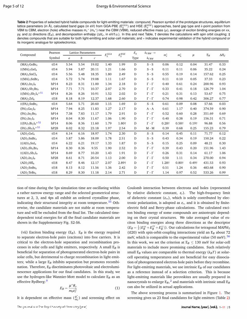
Table 2 Properties of selected hybrid halide compounds for light-emitting materials: compound, Pearson symbol of the prototype structures, equilibriumlattice parameters (in Å), calculated band gaps (in eV) from GGA-PBE (EGGA
g ) and HSE (EHSEg ) approaches, band gap type and k-point position from
VBM to CBM, electron (hole) effective masses me∗ (mh
∗) near the CBM (VBM), reduced effective mass (µ), average of exciton binding energies on xx,yy, and zz directions (EB), and decomposition enthalpy (∆Hd , in eV/f.u.). In this and next Table, † denotes the calculations with spin orbit coupling; ‡denotes compounds that are suitable for both light-emitting and solar-cell materials; and ∗ indicates experimental validation of the hybrid compound orits inorganic analogue for optoelectronics.
CompoundPearson Lattice Parameters
EGGAg EHSE
gEg kV BM → m∗e m∗h µ EB ∆Hd
Symbol a b c Type kCBM
(MA)2GeBr4 tI14 5.54 5.54 19.02 1.40 1.99 D S - S 0.06 0.12 0.04 31.47 0.33
‡(MA)2GeI4 tI14 5.94 5.87 20.11 1.21 1.66 D S - S 0.11 0.11 0.06 35.22 0.24
(MA)2SnCl4 tI14 5.56 5.48 18.35 1.80 2.49 D S - S 0.55 0.19 0.14 157.62 0.25
‡(MA)2SnBr4 tI14 5.72 5.74 19.08 1.11 1.67 D S - S 0.11 0.10 0.05 37.33 0.23
(MA)3In2I9 hP14 8.23 8.31 11.00 1.34 2.18 D Γ - Γ 0.40 0.61 0.24 200.96 0.93
(MA)3Sb2Br9 hP14 7.71 7.71 10.37 2.07 2.70 D Γ - Γ 0.33 0.41 0.18 126.79 1.04
‡(MA)3Sb2I9* 51 hP14 8.26 8.26 10.91 1.52 2.02 D Γ - Γ 0.21 0.31 0.13 53.67 0.75
(MA)2ZrI6 tI18 8.18 8.19 12.37 1.68 2.60 D Γ - Γ 0.74 0.98 0.42 306.27 0.77
‡(FA)2SnBr4 tI14 5.64 5.71 20.60 1.15 1.69 D S - S 0.61 0.09 0.08 57.66 0.03
(FA)3Ga2I9 hP14 7.94 8.25 11.83 1.27 2.17 D A - A 0.61 1.17 0.40 374.59 0.90
(FA)3In2Br9 hP14 7.38 7.83 11.17 1.79 2.91 D Γ - Γ 0.52 0.60 0.28 351.69 0.69
(FA)3In2I9 hP14 8.04 8.30 11.67 1.06 1.90 D Γ - Γ 0.40 0.38 0.19 156.31 0.71
‡(FA)3Bi2I9* 52 hP14 8.06 8.36 11.60 1.79 1.80† D Γ - Γ 0.28† 0.58† 0.19† 96.88 0.56
(FA)3Sb2I9* 53 hP28 8.02 8.32 23.18 1.97 2.54 D M - M 0.39 0.68 0.25 155.23 0.79
(AD)2GeI4 tI14 6.14 6.16 18.97 1.74 2.30 D S - S 0.14 0.45 0.11 71.77 0.12
(AD)2SnBr4 tI14 5.87 5.86 18.09 1.78 2.51 D S - S 0.43 0.34 0.19 150.24 0.22
‡(AD)2SnI4 tI14 6.22 6.21 19.17 1.33 1.87 D S - S 0.15 0.25 0.09 48.21 0.30
(AD)3Sb2Br9 hP14 8.30 8.36 9.55 1.90 2.52 D Γ - Γ 0.39 0.43 0.20 151.96 1.43
‡(AD)3Sb2I9 hP14 8.69 8.77 10.20 1.43 1.91 D Γ - Γ 0.26 0.31 0.14 61.17 1.06
(AD)3In2I9 hP28 8.61 8.71 20.54 1.13 2.00 D Γ - Γ 0.50 1.11 0.34 270.00 0.94
(AD)2HfI6 tI18 8.47 8.46 12.17 2.07 2.89† D Γ - Γ 1.28† 0.80† 0.49† 431.53 0.93
(AD)2SnBr6 tI18 8.13 8.12 11.56 1.36 2.42 D Γ - Γ 0.51 1.24 0.36 483.68 0.90
(AD)2TeBr6 tI18 8.29 8.30 11.18 2.14 2.71 D Γ - Γ 1.14 0.97 0.52 533.26 0.99
tion of time during the 5ps simulation time are oscillating withina rather narrow energy range and the selected geometrical struc-tures at 2, 3, and 4ps all exhibit an ordered crystalline phase,indicating their structural integrity at room temperature.55 Oth-erwise, the candidate materials are not stable at room tempera-ture and will be excluded from the final list. The calculated time-dependent total energies for all the final candidate materials areshown in the Supplementary Fig. S2-S6.
(vii) Exciton binding energy (EB). EB is the energy requiredto separate electron-hole pairs (excitons) into free carriers. It iscritical to the electron-hole separation and recombination pro-cesses in solar cells and light emitters, respectively. A small EB isbeneficial for separation of photogenerated electron-hole pairs insolar cells, but detrimental to charge recombination in light emit-ters; while a large EB inhibits separation but promotes recombi-nation. Therefore, EB discriminates photovoltaic and electrolumi-nescence applications for our final candidates. In this study, weuse the hydrogen-like Wannier-Mott model to calculate EB as aneffective Rydberg:9
EB =µ∗Ry
m0ε2r
(1)
It is dependent on effective mass ( µ∗
m0) and screening effect on
Coulomb interaction between electrons and holes (representedby relative dielectric constant, εr). The high-frequency limitof dielectric constant (ε∞), which is solely contributed by elec-tronic polarization, is adopted as εr, and it is obtained by finite-electric field and Berry-phase calculations. The calculated exci-ton binding energy of some compounds are anisotropic depend-ing on their crystal structures. We take averaged value of ex-citon binding energies along three directions as the descriptor(EB = 1
3 (ExxB +Eyy
B +EzzB )). Our calculations for tetragonal MAPbI3
(tI20) with spin-orbit-coupling interactions yield an EB about 72meV, which is comparable to the experimental value (50 meV).56
In this work, we set the criterion at EB ≤ 130 meV for solar-cellmaterials to include more promising candidates. Such relativelysmall EB values are comparable to thermal energy (kBT ) at solar-cell operating temperatures and are beneficial for easy dissocia-tion of photogenerated electron-hole pairs before they recombine.For light-emitting materials, we use intrinsic EB of our candidatesas a reference instead of a selection criterion. This is becauselight-emitting materials like perovskites are usually prepared innanocrystals to enlarge EB,2 and materials with intrinsic small EB
can also be utilized in actual applications.
The above screening process is summarized in Figure 1. Thescreening gives us 23 final candidates for light emitters (Table 2)
Journal Name, [year], [vol.],1–11 | 5
Page 5 of 12 Energy & Environmental Science

Table 3 Properties of selected hybrid halide compounds for solar-cell materials.
CompoundPearson Lattice Parameters
EGGAg EHSE
gEg kV BM → m∗e m∗h µ EB ∆Hd
Symbol a b c Type kCBM
‡(MA)2GeI4 tI14 5.94 5.87 20.11 1.21 1.66 D S - S 0.11 0.11 0.06 35.22 0.24
‡(MA)2SnBr4 tI14 5.72 5.74 19.08 1.11 1.67 D S - S 0.11 0.10 0.05 37.33 0.23
(MA)2SnI4 tI14 6.12 6.11 20.00 0.97 1.42 D S - S 0.18 0.10 0.06 33.81 0.30
‡(MA)3Sb2I9* 51 hP14 8.26 8.26 10.91 1.52 2.02 D Γ - Γ 0.21 0.31 0.13 53.67 0.75
(MA)3Bi2I9 hP14 8.35 8.35 11.00 1.85 1.82† I A - Γ 0.41† 0.62† 0.25† 124.88 0.59
(MA)2SnI6* 54 cF36 11.61 11.44 12.55 0.09 0.80 D Γ - Γ 0.22 1.16 0.18 94.82 0.43
(MA)2TeI6* 54 cF36 11.67 11.51 12.58 1.27 1.77 I Γ - L 0.25 1.24 0.21 104.21 0.78
‡(FA)2SnBr4 tI14 5.64 5.71 20.60 1.15 1.69 D S - S 0.61 0.09 0.08 57.66 0.03
‡(FA)3Bi2I9* 52 hP14 8.06 8.36 11.60 1.79 1.80† D Γ - Γ 0.28† 0.58† 0.19† 96.88 0.56
‡(AD)2SnI4 tI14 6.22 6.21 19.17 1.33 1.87 D S - S 0.15 0.25 0.09 48.21 0.30
‡(AD)3Sb2I9 hP14 8.69 8.77 10.20 1.43 1.91 D Γ - Γ 0.26 0.31 0.14 61.17 1.06
(AD)3Bi2I9 hP14 8.78 8.84 10.26 1.79 1.80† I M - Γ 0.38† 0.48† 0.21† 109.24 0.94
(AD)2TeI6 cF36 12.54 11.63 12.17 1.24 1.87 I Γ - L 0.27 1.09 0.22 120.85 0.93
and 13 final candidates for solar cells (Table 3). Among thesefinal candidates, 7 compounds are suitable for both applications.
Besides the seven materials descriptors discussed above, someother materials parameters such as defect tolerance and light ab-sorption are also closely related to the optoelectronic properties.An ideal defect tolerance should have following property: intrin-sic defects with low formation energies do not induce deep gapstates, while those creating deep gap states have high formationenergies.9,57–59 Such defect tolerance prevents the undesired re-combination of photoexcited electrons and holes. A completedefect property study requires considerations of all the possibledefects, such as various types of anionic and cationic vacancies,anti-sites defects, and interstitial defects, and even charged de-fects, in each candidate, which is beyond the scope of this high-throughput screening study. Moreover, our screening process al-ready limits the final candidates to a very small and specific struc-tural and compositional space out of the comprehensive materialsrepository of over 4500 compounds, and some predicted materi-als (including their inorganic analogues) have been demonstratedin recent experiments for optoelectronic applications (see Table2 and 3), indicating a robust credibility of our high-throughputscreening approach. As for the light absorption property, as dis-cussed in previous studies, it is largely dependent on the bond-ing characteristic, band-gap type and values, and band disper-sion,17,60 which have been partially addressed in the screeningprocess and will be discussed later with the electronic structuresfor the final candidates.
4 Discussion4.1 Composition and StructureIn this section, we discuss crystal structure and composition ofthe selected compounds. Table 2 and Table 3 show all the finalcandidates for light-emitting and photovoltaic materials, respec-tively. The final candidates based on different organic A cationstake the same structures and contain similar B and X elements.Note that EA- and DMA-based compounds are not included in thefinal lists, because they show relatively low decomposition en-
thalpy compared to their MA/FA/AD analogues according to ourcalculations. All the final candidates adopt five out of the 23 pro-totype structures, with their Pearson numbers being tI14, hP14,hP28, tI18, and cF36, see their structural illustrations in Figure3a-d and Figure S1 of Supporting Information. The B sites in thefive structures correspond to ions of different valence states from+2 to +4, and they greatly determine the compositions of the fi-nal candidates. Below we discuss the selected compounds in theorder of their B-site valence states.
The B2+ candidates all take the tI14 structure (Figure 3a) witha chemical formula of A2BX4. tI14 consists of corner-sharing oc-tahedra in a two-dimensional (2D) arrangement. B-site elementsof selected tI14 compounds include Ge and Sn. Note that Sn2+
or Ge2+ oxidation states are metastable and are prone to be ox-idized to +4, which could raise concerns about their oxidationstability. However, recent experimental10 and computational37
studies both indicate that the 2D hybrid perovskites based onSn2+ or Ge2+ show enhanced materials stability compared tothe 3D perovskites because of their low-dimensional structuralfeature, and the low-dimensional structure effectively preventsthe oxidation of Sn2+ during the film fabrication.10 Interestingly,unlike traditional perovskites, crystal structure of screened tI14compounds resemble that of the 2D hybrid perovskites, implyinga robust stability of these candidate materials. Moreover, evenfor traditional perovskites containing Sn2+ or Ge2+, some experi-mental techniques are actively proposed to improve their stabilityand to prevent the oxidation, such as using encapsulation of de-vices,11 and the solar cells based on MASnI3 perovskites havebeen demonstrated with an efficiency around 6%.61,62 In addi-ation, it is worth mentioning that some other tI14 compoundshave been synthesized and proposed for solar cells in prior ex-periments, including MA2CuX4
63 and MA2PdCl(Br)446,47. Our
calculations show that these compounds have large m∗h, and weexcluded them according to the m∗h ≤ 1.5m0 criterion. Our cal-culation results of large m∗h are also in good agreement with thereduced charge mobility and very low device efficiency observedin the above experimental studies. Notably, Zn and Mg-based
6 | 1–11Journal Name, [year], [vol.],
Page 6 of 12Energy & Environmental Science

(MA)2GeI4 (MA)3In2I9 (FA)3Sb2I9 (MA)2ZrI6(a) (b) (c) (d)
(a’) (b’) (c’) (d’)
(a’’) (b’’) (c’’) (d’’)
Ge In Sb Zr
I I I I
-1
0
1
2
3
Γ X S Y Γ Z U R T Z
Ener
gy (
eV)
Γ X Y Σ Γ Z Σ1 N P Y1 ZΓ M K Γ A L H A Γ M K Γ A L H A
0
2
4
PD
OS
(S
tate
s/eV
/Cel
l)
s p d
0
5
10
-4 -2 0 2 4 6
E (eV)
0
2
4s p d
0
5
10
-4 -2 0 2 4 6
E (eV)
0
10
20s p d
0
20
40
-4 -2 0 2 4 6
E (eV)
0
4
8s p d
0
20
40
-4 -2 0 2 4 6
E (eV)
Fig. 3 Representative candidates and their prototype structures: (a) (MA)2GeI4 in tI14, a tetragonal structure consisting of layers of corner-sharingBIIX6 octahedra, (b) (MA)3In2I9 in hP14, a hexagonal structure consisting of corrugated layers of corner-sharing BIIIX6 octahedra, (c) (FA)3Sb2I9 inhP28, a hexagonal structure consisting of dimers of face-sharing BIIIX6 octahedra, and (d) (MA)2ZrI6 in tI18, a tetragonal structure consisting of isolatedBIV X6 octahedra. Their calculated electronic band structures are shown in (a’-d’) and atomic orbital projected density of states with HSE06 correctionare shown in (a”-d”).
tI14 compounds show excellent optoelectronic properties in ourcalculations, but they were excluded due to large ∆Hdi f f
f .12
The B3+ candidates take two different crystal structures, hP14and hP28, both with the formula of A3B2X9 (Figure 3b and3c, respectively). Their difference lies in microscopic structureunits. hP14 consists of corner-sharing octahedra in 2D corrugatedlayers, while hP28 consists of face-sharing octahedra in zero-dimensional (0D) dimers. As competing phases of each other,hP14 and hP28 for the same composition usually have pretty closetotal energies. To decide which structure stays in the final list, wefirst followed our criterion for selecting stable competing phases(∆Hdi f f
f ≤ 0.015 eV/atom), and then kept the one with more suit-able electronic properties for light-emitter or solar-cell applica-tions. hP14 is usually more favorable due to higher electronicdimensionality64, but hP28 gives more appropriate properties forsome compositions according to our calculations. For example,hP28 MA3Sc2I9 yields a direct band gap of proper energy, whilehP14 yields an indirect band gap out of the optimal range. Infact, halogen substitution has been demonstrated to lead to phasetransition between hP14 and hP28 for A3B2X9 compounds25. The
B3+ elements of the selected compounds contain Ga, In, Sb, andBi. Interestingly, some compounds in hP28 (Cs3Bi2I9, MA3Bi2I9,and MA3Sb2I9) and hP14 (Cs3Sb2I9 and Rb3Sb2I9) have been fab-ricated for photovoltaic applications in prior experiments.24 Ac-cordingly, this class of materials, particularly the new compoundsdiscovered in this work, hold great promise with intrinsic highstability and non-toxicity for the optoelectronic applications.
The B4+ candidates adopt two very similar structures, tetrago-nal tI18 and cubic cF36 (Figure 3d and Figure S1p, respectively).These two structures have the same formula of A2BX6 and canconvert to each other through phase transition.65 They both con-sist of 0D isolated BX6 octahedra. According to our screening,promising B-site elements in these structures include Zr, Hf, Sn,and Te. Cs2SnI6 and Cs2TeI6 (cF36) have been incorporated in so-lar cell devices.54 These compounds were demonstrated to havehigh air and moisture stability, proper band gaps, and good elec-tron conductivity. Interestingly, it is noted that Cs2PdBr6 (cF36)has also been synthesized and shows promising properties andhigh stability;48 its hybrid analogue MA2PdBr6 (cF36) was notselected in our list because of a large m∗h of 1.98m0.
Journal Name, [year], [vol.],1–11 | 7
Page 7 of 12 Energy & Environmental Science

4.2 Electronic Structures
In this section, we discuss electronic band structures and atomicorbital projected density of states (PDOS) of representative can-didates to reveal electronic properties of all selected compounds.This is because compounds of each prototype structure have com-mon attributes in electronic structures. We selected (MA)2GeI4,(MA)3In2I9, (FA)3Sb2I9, and (MA)2ZrI6 to represent selectedcompounds of the prototype structures tI14, hP14, hP28, andtI18, respectively. Note that example of cF36 compounds is notshown here because cF36 is very similar to tI18. Figure 3a’-d’ and3a”-d” show the band structures and PDOS of the four represen-tative candidates. The calculated band gap and effective massesdata for all final candidates is listed in Table 2 and Table 3.
(MA)2GeI4, representing the tI14 candidates with B2+ cations,shows a direct band gap of 1.66 eV at S point (Figure 3a’). Bandsnear the conduction band minimum (CBM) and valence bandmaximum (VBM) are very dispersive, yielding small m∗e and m∗hof both 0.11m0. Its PDOS shows that conduction band (CB) ismainly contributed by Ge 4p orbitals while valence band (VB) ismostly derived from I 5p and Ge 4s orbitals (Figure 3a”).
(MA)3In2I9, as an example of the hP14 candidates, shows a di-rect band gap of 2.18 eV at Γ point (Figure 3b’). Near the bandedges, it has a m∗e of 0.40m0, and a m∗h of 0.61m0. Its VB is de-rived from In 4d and I 5p orbitals, and the CB is derived from In5s and I 5p orbitals (Figure 3b”). (FA)3Sb2I9, as an example ofhP28 candidates, shows a direct band gap of 2.54 eV at M point(Figure 3c’). The m∗e and m∗h were calculated to be 0.39m0 and0.68m0, respectively. Its VB consists of Sb 5s and I 5p orbitals,and the CB consists of Sb 5p and I 5p orbitals (Figure 3c”). Thesetwo candidates both contain B3+ cations but adopt different pro-totype structures. To discuss dependence of electronic structureson crystal structures, we compare the two candidates’ valencebands on two parts of the hexagonal k-path. On the Γ-A k-path,both the hP14 and hP28 candidates show non-dispersive valencebands and large m∗h. Γ-A corresponds to [001] direction for thehexagonal lattice in real space, and large calculated m∗h on Γ-Aindicates poor hole transport along [001]. This agrees well withpoor octahedral connectivity along [001] in the hP14 and hP28structures (Figure 3b and 3c). On the M-K k-path, valence bandsof the hP14 candidate is much more dispersive than those of hP28candidate. This is because M-K corresponds to real-space direc-tion in (001) plane, and the 2D connectivity in hP14 is much morebeneficial for hole transport than the 0D connectivity in hP28. No-tably, compounds in both of these structures have rather indistinctVBMs, making the band gap types ambiguous. For light-emittingapplications, the band gaps become more distinctly direct due toquantum confinement when the compounds are synthesized asnanocrystals.66,67
(MA)2ZrI6, representing the tI18 candidates with B4+ cations,shows a distinct direct band gap of 2.60 eV at Γ point, with verydispersive bands near the band edges (Figure 3d’). Its PDOSshows that both VB and CB are mainly contributed by Zr 4d andI 5p orbitals (Figure 3d”). As mentioned, B4+-based compoundsin the tI18 and cF36 structures consist of isolated octahedra, andtheir B-X bonds are not well connected in a 3D manner. However,
the BX6 octahedra are in close proximity to each other, makingit possible for tI18 and cF36 compounds to possess appropriateband gaps and effective masses for the optoelectronic applica-tions24. Interestingly, the previously synthesized Cs2SnI6 (cF36)shows large m∗h, which is not suitable for photovoltaics.54 Ourscreening results of novel tI18 and cF36 compounds show moresuitable properties, especially small and balanced carrier effectivemasses, and hold great promise for applications in light emittersand solar cells.
5 ConclusionIn summary, we have demonstrated a high-throughput approachto the discovery of hybrid halide compounds beyond perovskitesfor optoelectronic applications. The discovery process hasscreened a comprehensive quantum materials repository contain-ing 4507 hybrid compounds using a series of electronic and ener-getic descriptors including difference of formation enthalpy, de-composition enthalpy, band gap, charge carrier effective masses,and exciton binding energy to select promising candidates for op-toelectronic applications. A total number of 23 candidates forlight-emitting diodes and 13 candidates for solar energy conver-sion were selected. These candidates adopt five prototype struc-tures, including tetragonal structure consisting of layers of cor-ner sharing BIIX6 (tI14), hexagonal structure consisting of cor-rugated layers of corner-sharing BIIIX6 (hP14), hexagonal struc-ture consisting of dimers of face-sharing BIIIX6 (hP28), tetragonalstructure consisting of isolated BIV X6 (tI18), and cubic structureconsisiting of isolated BIV X6 (cF36). The tI14 candidates containBII=Ge, Sn; the hP14 and hP28 candidates contain BIII=Ga, In,Sb, Bi; and the tI18 and cF36 candidates contain BIV =Zr, Te, Sn,and Hf. It is important to note that this approach is transformativeto the discovery of other types of functional materials.
6 AcknowledgmentThis work was supported by the Global Research Outreach (GRO)Program of Samsung Advanced Institute of Technology under theaward number 20164974 and National Science Foundation un-der award number ACI-1550404. This work used the ExtremeScience and Engineering Discovery Environment (XSEDE), whichis supported by National Science Foundation grant number OCI-1053575, and computational resources supplied by the Depart-ment of Defense High Performance Computing ModernizationProgram (HPCMP).
References1 A. Kojima, K. Teshima, Y. Shirai, and T. Miyasaka,
Organometal Halide Perovskites as Visible-Light Sensitizersfor Photovoltaic Cells, J. Am. Chem. Soc. 131, 6050–6051(2009).
2 S. A. Veldhuis, P. P. Boix, N. Yantara, M. Li, T. C. Sum,N. Mathews, and S. G. Mhaisalkar, Perovskite Materials forLight-Emitting Diodes and Lasers, Adv. Mater. 28, 6804–6834(2016).
3 S. De Wolf, J. Holovsky, S.-J. Moon, P. Loper, B. Niesen,M. Ledinsky, F.-J. Haug, J.-H. Yum, and C. Ballif, Organometal-lic Halide Perovskites: Sharp Optical Absorption Edge and Its
8 | 1–11Journal Name, [year], [vol.],
Page 8 of 12Energy & Environmental Science

Relation to Photovoltaic Performance, J. Phys. Chem. Lett. 5,1035–1039 (2014).
4 C. Wehrenfennig, G. E. Eperon, M. B. Johnston, H. J. Snaith,and L. M. Herz, High Charge Carrier Mobilities and Lifetimes inOrganolead Trihalide Perovskites, Adv. Mater. 26, 1584–1589(2014).
5 A. Walsh, D. O. Scanlon, S. Chen, X. Gong, and S.-H. Wei,Self-Regulation Mechanism for Charged Point Defects in Hy-brid Halide Perovskites, Angew. Chem. Int. Ed. 54, 1791–1794(2015).
6 A. T. Barrows, A. J. Pearson, C. K. Kwak, A. D. Dunbar,A. R. Buckley, and D. G. Lidzey, Efficient Planar Heterojunc-tion Mixed-Halide Perovskite Solar Cells Deposited via Spray-Deposition, Energy Environ. Sci. 7, 2944–2950 (2014).
7 D. Bryant, N. Aristidou, S. Pont, I. Sanchez-Molina,T. Chotchunangatchaval, S. Wheeler, J. R. Durrant, and S. A.Haque, Light and Oxygen Induced Degradation Limits the Oper-ational Stability of Methylammonium Lead Triiodide PerovskiteSolar Cells, Energy Environ. Sci. 9, 1655–1660 (2016).
8 B. Conings, J. Drijkoningen, N. Gauquelin, A. Babayigit,J. D’Haen, L. D’Olieslaeger, A. Ethirajan, J. Verbeeck,J. Manca, E. Mosconi, et al., Intrinsic Thermal Instabilityof Methylammonium Lead Trihalide Perovskite, Adv. EnergyMater. 5, 1500477 (2015).
9 D. Yang, J. Lv, X. Zhao, Q. Xu, Y. Fu, Y. Zhan, A. Zunger,and L. Zhang, Functionality-Directed Screening of Pb-Free Hy-brid Organic–inorganic Perovskites with Desired Intrinsic Pho-tovoltaic Functionalities, Chem. Mater. 29, 524–538 (2017).
10 Y. Liao, H. Liu, W. Zhou, D. Yang, Y. Shang, Z. Shi, B. Li,X. Jiang, L. Zhang, L. N. Quan, et al., Highly Oriented Low-Dimensional Tin Halide Perovskites with Enhanced Stability andPhotovoltaic Performance, J. Am. Chem. Soc. 139, 6693–6699(2017).
11 F. Hao, C. C. Stoumpos, P. Guo, N. Zhou, T. J. Marks, R. P.Chang, and M. G. Kanatzidis, Solvent-Mediated Crystallizationof CH3NH3SnI3 Films for Heterojunction Depleted Perovskite So-lar Cells, J. Am. Chem. Soc. 137, 11445–11452 (2015).
12 R. Ali, G.-J. Hou, Z.-G. Zhu, Q.-B. Yan, Q.-R. Zheng, and G. Su,Predicted Lead-Free Perovskites for Solar Cells, Chem. Mater.30, 718–728 (2018).
13 M. R. Filip, S. Hillman, A. A. Haghighirad, H. J. Snaith, andF. Giustino, Band Gaps of the Lead-Free Halide Double Per-ovskites Cs2BiAgCl6 and Cs2BiAgBr6 from Theory and Experi-ment, J. Phys. Chem. Lett. 7, 2579–2585 (2016).
14 E. T. McClure, M. R. Ball, W. Windl, and P. M. Woodward,Cs2AgBiX6 (X= Br, Cl): New Visible Light Absorbing, Lead-FreeHalide Perovskite Semiconductors, Chem. Mater. 28, 1348–1354 (2016).
15 A. H. Slavney, T. Hu, A. M. Lindenberg, and H. I. Karunadasa,A Bismuth-Halide Double Perovskite with Long Carrier Recom-bination Lifetime for Photovoltaic Applications, J. Am. Chem.Soc. 138, 2138–2141 (2016).
16 F. Wei, Z. Deng, S. Sun, F. Xie, G. Kieslich, D. M. Evans, M. A.Carpenter, P. D. Bristowe, and A. K. Cheetham, The Synthe-sis, Structure and Electronic Properties of a Lead-Free Hybrid
Inorganic–organic Double Perovskite (MA2KBiCl6 (MA= Methy-lammonium), Mater. Horizons 3, 328–332 (2016).
17 X.-G. Zhao, J.-H. Yang, Y. Fu, D. Yang, Q. Xu, L. Yu, S.-H. Wei,and L. Zhang, Design of Lead-Free Inorganic Halide Perovskitesfor Solar Cells via Cation-Transmutation, J. Am. Chem. Soc.139, 2630–2638 (2017).
18 X.-G. Zhao, D. Yang, Y. Sun, T. Li, L. Zhang, L. Yu, andA. Zunger, Cu–In Halide Perovskite Solar Absorbers, J. Am.Chem. Soc. 139, 6718–6725 (2017).
19 T. Nakajima and K. Sawada, Discovery of Pb-Free PerovskiteSolar Cells via High-Throughput Simulation on the K Computer,J. Phys. Chem. Lett. 8, 4826–4831 (2017).
20 Z. Xiao, K.-Z. Du, W. Meng, J. Wang, D. B. Mitzi, and Y. Yan,Intrinsic Instability of Cs2In(I)M(III)X6 (M= Bi, Sb; X= Halo-gen) Double Perovskites: A Combined Density Functional Theoryand Experimental Study, J. Am. Chem. Soc. 139, 6054–6057(2017).
21 J. Luo, X. Wang, S. Li, J. Liu, Y. Guo, G. Niu, L. Yao, Y. Fu,L. Gao, Q. Dong, et al., Efficient and Stable Emission of Warm-White Light from Lead-Free Halide Double Perovskites, Nature563, 541 (2018).
22 X.-G. Zhao, D. Yang, J.-C. Ren, Y. Sun, Z. Xiao, and L. Zhang,Rational Design of Halide Double Perovskites for OptoelectronicApplications, Joule 2, 1662–1673 (2018).
23 M.-G. Ju, M. Chen, Y. Zhou, J. Dai, L. Ma, N. P. Padture, andX. C. Zeng, Toward Eco-Friendly and Stable Perovskite Materialsfor Photovoltaics, Joule 2, 1231–1241 (2018).
24 A. Jodlowski, D. Rodríguez-Padrón, R. Luque, andG. de Miguel, Alternative Perovskites for Photovoltaics,Adv. Energy Mater. 8, 1703120 (2018).
25 F. Jiang, D. Yang, Y. Jiang, T. Liu, X. Zhao, Y. Ming, B. Luo,F. Qin, J. Fan, H. Han, et al., Chlorine-Incorporation-InducedFormation of the Layered Phase for Antimony-Based Lead-FreePerovskite Solar Cells, J. Am. Chem. Soc. 140, 1019–1027(2018).
26 N. Pai, J. Lu, T. R. Gengenbach, A. Seeber, A. S. Chesman,L. Jiang, D. C. Senevirathna, P. C. Andrews, U. Bach, Y.-B.Cheng, et al., Silver Bismuth Sulfoiodide Solar Cells: TuningOptoelectronic Properties by Sulfide Modification for EnhancedPhotovoltaic Performance, Adv. Energy Mater. 9, 1803396(2019).
27 S. Curtarolo, W. Setyawan, G. L. W. Hart, M. Jahnatek, R. V.Chepulskii, R. H. Taylor, S. Wang, J. Xue, K. Yang, O. Levy,M. Mehl, H. T. Stokes, D. O. Demchenko, , and D. Morgan,AFLOW: an Automatic Framework for High-Throughput Mate-rials Discovery, Comput. Mater. Sci. 58, 218–226 (2012).
28 G. Kresse and D. Joubert, From Ultrasoft Pseudopotentials tothe Projector Augmented-Wave Method, Phys. Rev. B 59, 1758–1775 (1999).
29 J. P. Perdew, K. Burke, and M. Ernzerhof, Generalized GradientApproximation Made Simple, Phys. Rev. Lett. 77, 3865–3868(1996).
30 S. Grimme, J. Antony, S. Ehrlich, and H. Krieg, A Consistentand Accurate Ab Initio Parametrization of Density Functional
Journal Name, [year], [vol.],1–11 | 9
Page 9 of 12 Energy & Environmental Science

Dispersion Correction (DFT-D) for the 94 Elements H-Pu, J.Chem. Phys. 132, 154104 (2010).
31 J. Klimeš, D. R. Bowler, and A. Michaelides, Chemical Accuracyfor the van der Waals Density Functional, J. Phys.: Condens.Matter 22, 022201 (2009).
32 J. Heyd, G. E. Scuseria, and M. Ernzerhof, Hybrid Function-als Based on a Screened Coulomb Potential, Chem. Phys. 118,8207–8215 (2003).
33 A. V. Krukau, O. A. Vydrov, A. F. Izmaylov, and G. E. Scuse-ria, Influence of the Exchange Screening Parameter on the Per-formance of Screened Hybrid Functionals, J. Chem. Phys. 125,224106 (2006).
34 S. Curtarolo, W. Setyawan, S. Wang, J. Xue, K. Yang, R. H.Taylor, L. J. Nelson, G. L. W. Hart, S. Sanvito, M. B. Nardelli,N. Mingo, and O. Levy, AFLOWLIB.ORG: A Distributed Mate-rials Properties Repository from High-Throughput ab Initio Cal-culations, Comput. Mater. Sci. 58, 227–235 (2012).
35 A. Jain, S. P. Ong, G. Hautier, W. Chen, W. D. Richards,S. Dacek, S. Cholia, D. Gunter, D. Skinner, G. Ceder, andK. A. Persson, Commentary: The Materials Project: A Materi-als Genome Approach to Accelerating Materials Innovation, APLMaterials 1, 011002 (2013).
36 C. Zheng and O. Rubel, Aziridinium Lead Iodide: A Stable, Low-Band-Gap Hybrid Halide Perovskite for Photovoltaics, J. Phys.Chem. Lett. 9, 874–880 (2018).
37 L. Wu, P. Lu, Y. Li, Y. Sun, J. Wong, and K. Yang,First-Principles Characterization of Two-Dimensional(CH3(CH2)3NH3)2(CH3NH3)n−1GenI3n+1 Perovskite, J. Mater.Chem. A 6, 24389–24396 (2018).
38 J. Even, L. Pedesseau, J.-M. Jancu, and C. Katan, Importanceof Spin–Orbit Coupling in Hybrid Organic/Inorganic Perovskitesfor Photovoltaic Applications, J. Phys. Chem. Lett. 4, 2999–3005 (2013).
39 W. Shockley and H. J. Queisser, Detailed Balance Limit of Effi-ciency of P-N Junction Solar Cells, J. Appl. Phys. 32, 510–519(1961).
40 E. F. Schubert, Light-emitting diodes (E. Fred Schubert, 2018).41 J. Nelson, The physics of solar cells (World Scientific Publishing
Company, 2003).42 L. Zeng, Y. Yi, C. Hong, J. Liu, N. Feng, X. Duan, L. Kimerling,
and B. Alamariu, Efficiency Enhancement in Si Solar Cells byTextured Photonic Crystal Back Reflector, Appl. Phys. Lett. 89,111111 (2006).
43 S. D. Stranks, G. E. Eperon, G. Grancini, C. Menelaou, M. J.Alcocer, T. Leijtens, L. M. Herz, A. Petrozza, and H. J. Snaith,Electron-Hole Diffusion Lengths Exceeding 1 Micrometer in anOrganometal Trihalide Perovskite Absorber, Science 342, 341–344 (2013).
44 X. Y. Chin, D. Cortecchia, J. Yin, A. Bruno, and C. Soci, Lead Io-dide Perovskite Light-Emitting Field-Effect Transistor, Nat. Com-mun. 6, 7383 (2015).
45 S. Siegel and E. Gebert, The Structures of Hexagonal CsCdCl3and Tetragonal Cs2CdCl4, Acta Cryst. 17, 790–790 (1964).
46 T. J. Huang, Z. X. Thiang, X. Yin, C. Tang, G. Qi,
and H. Gong, (CH3NH3)2PdCl4: A Compound with Two-Dimensional Organic–Inorganic Layered Perovskite Structure,Chem. Eur. J. 22, 2146–2152 (2016).
47 X. Liu, T. J. Huang, L. Zhang, B. Tang, N. Zhang, D. Shi,and H. Gong, Highly Stable, New, Organic-Inorganic Perovskite(CH3NH3)2PdBr4: Synthesis, Structure, and Physical Proper-ties, Chem. Eur. J. 24, 4991–4998 (2018).
48 N. Sakai, A. A. Haghighirad, M. R. Filip, P. K. Nayak, S. Nayak,A. Ramadan, Z. Wang, F. Giustino, and H. J. Snaith, Solution-Processed Cesium Hexabromopalladate (IV), Cs2PdBr6, for Op-toelectronic Applications, J. Am. Chem. Soc. 139, 6030–6033(2017).
49 R. Roccanova, W. Ming, V. R. Whiteside, M. A. McGuire, I. R.Sellers, M.-H. Du, and B. Saparov, Synthesis, Crystal and Elec-tronic Structures, and Optical Properties of (CH3NH3)2CdX4
(X= Cl, Br, I), Inorg. Chem. 56, 13878–13888 (2017).50 M. A. Green, A. Ho-Baillie, and H. J. Snaith, The Emergence of
Perovskite Solar Cells, Nat. Photon. 8, 506–514 (2014).51 P. Harikesh, H. K. Mulmudi, B. Ghosh, T. W. Goh, Y. T. Teng,
K. Thirumal, M. Lockrey, K. Weber, T. M. Koh, S. Li, et al.,Rb as an Alternative Cation for Templating Inorganic Lead-FreePerovskites for Solution Processed Photovoltaics, Chem. Mater.28, 7496–7504 (2016).
52 A. J. Lehner, D. H. Fabini, H. A. Evans, C.-A. Hébert, S. R.Smock, J. Hu, H. Wang, J. W. Zwanziger, M. L. Chabinyc,and R. Seshadri, Crystal and Electronic Structures of ComplexBismuth Iodides A3Bi2I9 (A= K, Rb, Cs) Related to Perovskite:Aiding the Rational Design of Photovoltaics, Chem. Mater. 27,7137–7148 (2015).
53 K. M. Boopathi, P. Karuppuswamy, A. Singh, C. Hanmandlu,L. Lin, S. A. Abbas, C. C. Chang, P. C. Wang, G. Li,and C. W. Chu, Solution-Processable Antimony-Based Light-Absorbing Materials Beyond Lead Halide Perovskites, J. Mater.Chem. A 5, 20843–20850 (2017).
54 A. E. Maughan, A. M. Ganose, M. M. Bordelon, E. M. Miller,D. O. Scanlon, and J. R. Neilson, Defect Tolerance to Intol-erance in the Vacancy-Ordered Double Perovskite Semiconduc-tors Cs2SnI6 and Cs2TeI6, J. Am. Chem. Soc. 138, 8453–8464(2016).
55 S. Lu, Q. Zhou, Y. Ouyang, Y. Guo, Q. Li, and J. Wang, Accel-erated Discovery of Stable Lead-Free Hybrid Organic-InorganicPerovskites via Machine Learning, Nat. Commun. 9, 3405(2018).
56 K. Tanaka, T. Takahashi, T. Ban, T. Kondo, K. Uchida, andN. Miura, Comparative Study on the Excitons in Lead-Halide-Based Perovskite-Type Crystals CH3NH3PbBr3 CH3NH3PbI3,Solid State Commun. 127, 619–623 (2003).
57 W.-J. Yin, T. Shi, and Y. Yan, Unusual Defect Physics inCH3NH3PbI3 Perovskite Solar Cell Absorber, Appl. Phys. Lett.104, 063903 (2014).
58 Z. Xiao, W. Meng, J. Wang, and Y. Yan, Thermodynamic Sta-bility and Defect Chemistry of Bismuth-Based Lead-Free DoublePerovskites, ChemSusChem 9, 2628–2633 (2016).
59 T. Li, X. Zhao, D. Yang, M.-H. Du, and L. Zhang, Intrinsic De-fect Properties in Halide Double Perovskites for Optoelectronic
10 | 1–11Journal Name, [year], [vol.],
Page 10 of 12Energy & Environmental Science

Applications, Phys. Rev. Appl. 10, 041001 (2018).60 K. Kuhar, A. Crovetto, M. Pandey, K. S. Thygesen, B. Seger,
P. C. Vesborg, O. Hansen, I. Chorkendorff, and K. W. Jacobsen,Sulfide Perovskites for Solar Energy Conversion Applications:Computational Screening and Synthesis of the Selected Com-pound LaYS3, Energy Environ. Sci. 10, 2579–2593 (2017).
61 F. Hao, C. C. Stoumpos, D. H. Cao, R. P. Chang, and M. G.Kanatzidis, Lead-Free Solid-State Organic–Inorganic HalidePerovskite Solar Cells, Nat. Photon. 8, 489 (2014).
62 N. K. Noel, S. D. Stranks, A. Abate, C. Wehrenfennig,S. Guarnera, A.-A. Haghighirad, A. Sadhanala, G. E. Eperon,S. K. Pathak, M. B. Johnston, et al., Lead-Free Organic–Inorganic Tin Halide Perovskites for Photovoltaic Applications,Energy Environ. Sci. 7, 3061–3068 (2014).
63 A. M. Elseman, A. E. Shalan, S. Sajid, M. M. Rashad,A. M. Hassan, and M. Li, Copper-Substituted Lead Per-ovskite Materials Constructed with Different Halides for Work-ing (CH3NH3)2CuX4-Based Perovskite Solar Cells from Experi-mental and Theoretical View, ACS Appl. Mater. Interfaces 10,11699–11707 (2018).
64 Z. Xiao, W. Meng, J. Wang, D. B. Mitzi, and Y. Yan, Search-ing for Promising New Perovskite-Based Photovoltaic Absorbers:the Importance of Electronic Dimensionality, Mater. Horizons4, 206–216 (2017).
65 S. Abrahams, J. Ihringer, and P. Marsh, Structural and ThermalDependence of Normal-Mode Condensations in K2TeBr6, ActaCrystallogr. Sect. B 45, 26–34 (1989).
66 B. Delley and E. Steigmeier, Quantum Confinement in SiNanocrystals, Phys. Rev. B 47, 1397 (1993).
67 J. K. Ellis, M. J. Lucero, and G. E. Scuseria, The Indirect toDirect Band Gap Transition in Multilayered MoS2 as Predictedby Screened Hybrid Density Functional Theory, Appl. Phys. Lett.99, 261908 (2011).
Journal Name, [year], [vol.],1–11 | 11
Page 11 of 12 Energy & Environmental Science

1
Energy & Environmental Science: EE-ART-04-2019-001371.R1
TITLE: High-throughput Computational Design of Organic-inorganic Hybrid Halide Semiconductors Beyond Perovskites for Optoelectronics
Broader context:
Organic-inorganic lead halide perovskites are promising for the next-generation solar cells and light-emitting applications because of their exceptional optoelectronic properties and low-temperature solution processability. However, this class of materials are facing two major challenges including intrinsic poor stability and the presence of toxic lead for their practical applications. To overcome these challenges, great efforts are being devoted to the development of tin-based perovskites and double perovskites, as well as new approaches to protect devices like using encapsulation. In this work, instead of focusing on perovskites, we present a powerful approach to search for novel lead-free hybrid halide semiconductors beyond perovskites from a large variety of prototype structures using high-throughput computations and data-mining techniques. 23 candidates for light-emitting diodes and 13 candidates for solar cells were rapidly identified. All these candidates show appropriate electronic properties and robust stability from ab-initio molecular dynamics simulations. This work demonstrates a new pathway for the large-scale design of novel organic-inorganic optoelectronic materials at a high speed by exploring a large variety of prototype structures. It is important to highlight that this approach is transformative to the discovery of other types of functional materials.
Page 12 of 12Energy & Environmental Science