hip4086, hip4086a datasheet - intersil.com for switched reluctance applications. the hip4086/a have...
TRANSCRIPT

FN4220Rev 1.00
January 12, 2017
HIP4086, HIP4086A80V, 500mA, 3-Phase MOSFET Driver
DATASHEET
The HIP4086 and HIP4086A (referred to as the HIP4086/A) are 3-phase N-channel MOSFET drivers. Both parts are specifically targeted for PWM motor control. These drivers have flexible input protocol for driving every possible switch combination. The user can even override the shoot-through protection for switched reluctance applications.
The HIP4086/A have a wide range of programmable dead times (0.5µs to 4.5µs) which makes them very suitable for the low frequencies (up to 100kHz) typically used for motor drives.
The only difference between the HIP4086 and the HIP4086A is that the HIP4086A has the built-in charge pumps disabled. This is useful in applications that require very quiet EMI performance (the charge pumps operate at 10MHz). The advantage of the HIP4086 is that the built-in charge pumps allow indefinitely long on times for the high-side drivers.
To insure that the high-side driver boot capacitors are fully charged prior to turning on, a programmable bootstrap refresh pulse is activated when VDD is first applied. When active, the refresh pulse turns on all three of the low-side bridge FETs while holding off the three high-side bridge FETs to charge the high-side boot capacitors. After the refresh pulse clears, normal operation begins.
Another useful feature of the HIP4086/A is the programmable undervoltage set point. The set point range varies from 6.6V to 8.5V.
Features• Independently drives 6 N-channel MOSFETs in 3-phase
bridge configuration
• Bootstrap supply maximum voltage up to 95VDC with bias supply from 7V to 15V
• 1.25A peak turn-off current
• User programmable dead time (0.5µs to 4.5µs)
• Bootstrap and optional charge pump maintain the high-side driver bias voltage.
• Programmable bootstrap refresh time
• Drives 1000pF load with typical rise time of 20ns and fall time of 10ns
• Programmable undervoltage set point
Applications• Brushless Motors (BLDC)
• 3-phase AC motors
• Switched reluctance motor drives
• Battery powered vehicles
• Battery powered tools
Related Literature• AN9642, “HIP4086 3-Phase Bridge Driver Configurations
and Applications”
• AN1829, “HIP4086 3-Phase BLDC Motor Drive Demonstration Board, User Guide”
TABLE 1. KEY DIFFERENCES BETWEEN FAMILY OF PARTS
PART NUMBERCHARGE
PUMP
HIP4086 Yes
HIP4086A No
FIGURE 1. TYPICAL APPLICATION FIGURE 2. CHARGE PUMP OUTPUT CURRENT
Controller
AHO
CLO
BLO
ALO
CHO
BHO
CLI
BLI
ALI
CHI
BHI
AHICHS
AHS
BHS
CHB
AHB
BHB
VDD
RDEL
VDD
Speed
Brake
Battery24V...48V
HIP
408
6/A
VSS
-60 -40 -20 0 20 40 60 80 100 120 140 160
200
150
100
50
0
JUNCTION TEMPERATURE (°C)
OU
TP
UT
CU
RR
EN
T (
µA
)
VxHB - VxHS = 10V
FN4220 Rev 1.00 Page 1 of 17January 12, 2017
HIP4086, HIP4086A
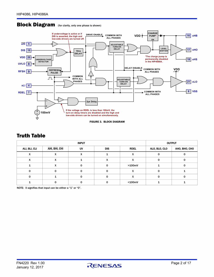
Block Diagram (for clarity, only one phase is shown)
FIGURE 3. BLOCK DIAGRAM
RDEL 7
xLI 4
RFSH 9
UVLO 8
VDD 20
DIS 10
xHI 5
2µs Delay
REFRESH PULSE
UNDERVOLTAGE DETECTOR
10ns DELAY
ADJUSTABLE TURN-ON
DELAY
LEVEL SHIFTER
CHARGE PUMP*
xHO17
xHB16
xHS18
xLO21
VSS6
VDD
100mV
VDD
*The charge pump is permanently disabled in the HIP4086A.
COMMON WITH ALL PHASES
COMMON WITH ALL PHASES
COMMON WITH ALL PHASES
COMMON WITH ALL PHASES
EN
If the voltage on RDEL is less than 100mV, the turn-on delay timers are disabled and the high and low-side drivers can be turned on simultaneously.
If undervoltage is active or if DIS is asserted, the high and low-side drivers are turned off.
ADJUSTABLE TURN-ON
DELAY
DELAY DISABLE
DRIVE ENABLE
Truth TableINPUT OUTPUT
ALI, BLI, CLI AHI, BHI, CHI UV DIS RDEL ALO, BLO, CLO AHO, BHO, CHO
X X X 1 X 0 0
X X 1 X X 0 0
1 X 0 0 >100mV 1 0
0 0 0 0 X 0 1
0 1 0 0 X 0 0
1 0 0 0 <100mV 1 1
NOTE: X signifies that input can be either a “1” or “0”.
FN4220 Rev 1.00 Page 2 of 17January 12, 2017

HIP4086, HIP4086A
Pin ConfigurationHIP4086, HIP4086A(24 LD PDIP, SOIC)
TOP VIEW
1BHB
2BHI
3BLI
4ALI
5AHI
6VSS
7RDEL
8UVLO
9RFSH
10DIS
11CLI
12CHI
24 BHO
23 BHS
22 BLO
21 ALO
20 VDD
19 CLO
18 AHS
17 AHO
16 AHB
15 CHS
14 CHO
13 CHB
Pin DescriptionsPIN NUMBER SYMBOL DESCRIPTION
161
13
AHBBHBCHB(xHB)
High-Side Bias Connections. One external bootstrap diode and one capacitor are required for each. Connect cathode of bootstrap diode and positive side of bootstrap capacitor to each xHB pin.
182315
AHSBHSCHS(xHS)
High-Side Source Connections. Connect the sources of the high-side power MOSFETs to these pins. The negative side of the bootstrap capacitors are also connected to these pins.
52
12
AHIBHICHI(xHI)
High-Side Logic Level Inputs. Logic at these three pins controls the three high-side output drivers, AHO (Pin 17), BHO (Pin 24) and CHO (Pin 14). When xHI is low, xHO is high. When xHI is high, xHO is low. Unless the dead time is disabled by connecting RDEL (Pin 7) to ground, the low-side input of each phase will override the corresponding high-side input on that phase - see “Truth Table” on page 2. If RDEL is tied to ground, dead time is disabled and the outputs follow the inputs with no shoot-through protection. DIS (Pin 10) also overrides the high-side inputs. xHI can be driven by signal levels of 0V to 15V (no greater than VDD).
43
11
ALIBLICLI(xLI)
Low-Side Logic Level Inputs. Logic at these three pins controls the three low-side output drivers ALO (Pin 21), BLO (Pin 22) and CLO (Pin 19). If the upper inputs are grounded then the lower inputs control both xLO and xHO drivers, with the dead time set by the resistor at RDEL (Pin 7). DIS (Pin 10) high level input overrides xLI, forcing all outputs low. xLI can be driven by signal levels of 0V to 15V (no greater than VDD).
6 VSS Ground. Connect the sources of the low-side power MOSFETs to this pin.
7 RDEL Delay Time Set Point. Connect a resistor from this pin to VDD to set timing current that defines the dead time between drivers - see Figure 19 on page 10. All drivers turn off with minimal delay, RDEL resistor prevents shoot-through by delaying the turn-on of all drivers. When RDEL is tied to VSS, both upper and lowers can be commanded on simultaneously. While not necessary in most applications, a decoupling capacitor of 0.1µF or smaller may be connected between RDEL and VSS.
8 UVLO Undervoltage Set Point. A resistor can be connected between this pin and VSS to program the undervoltage set point - see Figure 20 on page 10. With this pin not connected, the under voltage disable is typically 6.6V. When this pin is tied to VDD, the under voltage disable is typically 6.2V.
9 RFSH Refresh Pulse Setting. An external capacitor can be connected from this pin to VSS to increase the length of the start up refresh pulse - see Figure 18 on page 9. If this pin is not connected, the refresh pulse is typically 1.5µs.
FN4220 Rev 1.00 Page 3 of 17January 12, 2017

HIP4086, HIP4086A
10 DIS Disable Input. Logic level input that when taken high sets all six outputs low. DIS high overrides all other inputs. With DIS low, the outputs are controlled by the other inputs. DIS can be driven by signal levels of 0V to 15V (no greater than VDD).
172414
AHOBHOCHO(xHO)
High-Side Outputs. Connect to the gates of the high-side power MOSFETs in each phase.
20 VDD Positive Supply. Decouple this pin to VSS (Pin 6).
212219
ALOBLOCLO(xLO)
Low-Side Outputs. Connect the gates of the low-side power MOSFETs to these pins.
NOTE: x = A, B or C.
Pin Descriptions (Continued)
PIN NUMBER SYMBOL DESCRIPTION
Ordering InformationPART NUMBER
(Note 3)PART
MARKINGTEMP RANGE
(°C)CHARGE
PUMP PACKAGEPKG.
DWG. #
HIP4086AB (Note 1) HIP4086AB -40 to +125 Yes 24 Ld SOIC M24.3
HIP4086ABZ (Notes 1, 2) HIP4086ABZ -40 to +125 Yes 24 Ld SOIC (RoHS Compliant) M24.3
HIP4086APZ (Note 2) HIP4086APZ -40 to +125 Yes 24 Ld PDIP (RoHS Compliant) E24.3
HIP4086AABZ (Notes 1, 2) HIP4086AABZ -40 to +125 No 24 Ld SOIC (RoHS Compliant) M24.3
HIP4086DEMO1Z HIP4086 Demonstration Board
NOTES:
1. Add “T”, suffix for 1k unit tape and reel option. Please refer to TB347 for details on reel specifications.
2. These Intersil Pb-free plastic packaged products employ special Pb-free material sets, molding compounds/die attach materials, and 100% matte tin plate plus anneal (e3 termination finish, which is RoHS compliant and compatible with both SnPb and Pb-free soldering operations). Intersil Pb-free products are MSL classified at Pb-free peak reflow temperatures that meet or exceed the Pb-free requirements of IPC/JEDEC J STD-020.
3. For Moisture Sensitivity Level (MSL), please see device information page for HIP4086, HIP4086A. For more information on MSL, please see Technical Brief TB363.
FN4220 Rev 1.00 Page 4 of 17January 12, 2017
HIP4086, HIP4086A
Absolute Maximum Ratings (Note 7) Thermal InformationSupply Voltage, VDD Relative to GND. . . . . . . . . . . . . . . . . . . . . -0.3V to 16VLogic Inputs (xLI, xHI) . . . . . . . . . . . . . . . . . . . . . (GND - 0.3V) to VDD + 0.3VVoltage on xHS . . . . . . . . . . . . . . -6V (Transient) to 85V (-40°C to +150°C)Voltage on xHB . . . . . . . . . . . . . . . . . . . . . . . . . . . . (VxHS - 0.3V) to VxHS +VDDVoltage on xLO . . . . . . . . . . . . . . . . . . . . . . . . . . . . . (VSS - 0.3V) to VDD +0.3VVoltage on xHO . . . . . . . . . . . . . . . . . . . . . . . . . . . (VxHS - 0.3V) to VxHB +0.3VPhase Slew Rate (on xHS) . . . . . . . . . . . . . . . . . . . . . . . . . . . . . . . . . . 20V/ns
Maximum Recommended Operating ConditionsSupply Voltage, VDD Relative to GND. . . . . . . . . . . . . . . . . . . . . . . 7V to 15VLogic Inputs (xLI, xHI) . . . . . . . . . . . . . . . . . . . . . . . . . . . . . . . . . . . 0V to VDDVoltage on xHB . . . . . . . . . . . . . . . . . . . . . . . . . . . . . . . . . . . . . . . VxHS + VDDVoltage on xHS . . . . . . . . . . . . . . . . . . . . . . . . . . . . . . . . . . . . . . . . . 0V to 80VAmbient Temperature Range . . . . . . . . . . . . . . . . . . . . . . .-40°C to +125°CJunction Temperature Range . . . . . . . . . . . . . . . . . . . . . . .-40°C to +150°CRDEL range . . . . . . . . . . . . . . . . . . . . . . . . . . . . . . . . . . . . . . . 10kΩ to 100kΩ
Thermal Resistance (Typical) JA (°C/W) JC (°C/W)SOIC Package (Notes 4, 6) . . . . . . . . . . . . . 75 22SOIC Package HIP4086AABZ (Notes 5, 6) 51 22PDIP* Package (Notes 4, 6) . . . . . . . . . . . . 70 29
Storage Temperature Range. . . . . . . . . . . . . . . . . . . . . . . .-65°C to +150°COperating Junction Temp Range . . . . . . . . . . . . . . . . . . . .-40°C to +150°CPb-Free Reflow Profile . . . . . . . . . . . . . . . . . . . . . . . . . . . . . . . . . . see TB493
*Pb-free PDIPs can be used for through-hole wave solder processing only.They are not intended for use in Reflow solder processing applications.
CAUTION: Do not operate at or near the maximum ratings listed for extended periods of time. Exposure to such conditions may adversely impact productreliability and result in failures not covered by warranty.
NOTES:
4. JA is measured with the component mounted on a low effective thermal conductivity test board in free air. See Tech Brief TB379 for details.
5. JA is measured with the component mounted on a high effective thermal conductivity test board in free air. See Tech Brief TB379 for details.
6. For JC, the “case temp” location is taken at the package top center.
7. Replace x with A, B, or C.
DC Electrical Specifications VDD = VxHB = 12V, VSS = VxHS = 0V, RDEL = 20k, RUV = , Gate Capacitance (CGATE) = 1000pF, unless otherwise specified. Boldface limits apply across the operating junction temperature range, -40°C to +150°C.
PARAMETER TEST CONDITIONS
TJ = +25°C TJ = -40°C TO +150°C
UNITMIN
(Note 9) TYPMAX
(Note 9)MIN
(Note 9)MAX
(Note 9)
SUPPLY CURRENTS
VDD Quiescent Current xHI = 5V, xLI = 5V (HIP4086) 2.7 3.4 5.1 1.96 5.3 mA
xHI = 5V, xLI = 5V (HIP4086A) 2.3 2.8 3.1 1.8 3.3 mA
VDD Operating Current f = 20kHz, 50% Duty Cycle (HIP4086) 5.4 8.25 13 4 13.5 mA
f = 20kHz, 50% Duty Cycle (HIP4086A) 3.1 4.0 4.6 2.7 5.1 mA
xHB On Quiescent Current xHI = 0V (HIP4086) - 40 110 - 140 µA
xHI = 0V (HIP4086A) - 90 115 - 225 µA
xHB Off Quiescent Current xHI = VDD (HIP4086) 0.6 0.8 1.3 0.5 1.4 mA
xHI = VDD (HIP4086A) 0.8 1.0 1.2 0.7 1.25 mA
xHB Operating Current f = 20kHz, 50% Duty Cycle (HIP4086) 0.7 0.9 1.3 - 2.0 mA
f = 20kHz, 50% Duty Cycle (HIP4086A) 0.8 0.9 1.1 - 1.25 mA
xHB, xHS Leakage Current VxHS = 80V, VxHB = 93V 7 30 45 - 50 µA
Charge Pump, HIP4086 Only, (Note 8)
QPUMP Output Voltage No Load 11 12.5 14.6 10 14.75 V
QPUMP Output Current VxHS = 12V, VxHB = 22V 40 100 160 - 185 µA
UNDERVOLTAGE PROTECTION
VDD Rising Undervoltage Threshold RUV open 6.2 7.1 8.0 6.1 8.1 V
VDD Falling Undervoltage Threshold RUV open 5.75 6.6 7.5 5.6 7.6 V
Minimum Undervoltage Threshold RUV = VDD 5 6.2 6.8 4.8 6.9 V
FN4220 Rev 1.00 Page 5 of 17January 12, 2017

HIP4086, HIP4086A
INPUT PINS: ALI, BLI, CLI, AHI, BHI, CHI, AND DIS
Low Level Input Voltage - - 1.0 - 0.8 V
High Level Input Voltage 2.5 - - 2.7 - V
Input Voltage Hysteresis - 35 - - - mV
Low Level Input Current VIN = 0V -60 -100 -155 -55 -165 µA
High Level Input Current VIN = 5V -1 - +1 -10 +10 µA
GATE DRIVER OUTPUT PINS: ALO, BLO, CLO, AHO, BHO, AND CHO
Low Level Output Voltage (VOUT - VSS) ISINKING = 30mA - 100 - - 210 mV
Peak Turn-On Current VOUT = 0V 0.3 0.5 0.7 - 1.0 A
NOTES:
8. The specified charge pump current is the total amount available to drive external loads across xHO and xHS.
9. Compliance to datasheet limits is assured by one or more methods: production test, characterization and/or design.
AC Electrical Specifications VDD = VxHB = 12V, VSS = VxHS = 0V, CGATE = 1000pF, RDEL = 10k, unless otherwise specified. Boldface limits apply across the operating junction temperature range, -40°C to +150°C.
PARAMETER TEST CONDITIONS
TJ = +25°C TJ = -40°C TO +150°C
UNITMIN
(Note 9) TYPMAX
(Note 9)MIN
(Note 9)MAX
(Note 9)
TURN-ON DELAY AND PROPAGATION DELAY
Dead Time (Figure 4) RDEL = 100kΩ 3 4.5 7.2 3 8 µs
RDEL = 10kΩ 0.38 0.5 0.75 0.3 0.8 µs
Dead Time Channel Matching RDEL = 10kΩ - 7 15 - 20 %
Lower Turn-Off Propagation Delay(xLI to xLO Turn-Off) (Figures 4 or 5)
No load - 30 55 - 75 ns
Upper Turn-Off Propagation Delay(xHI to xHO Turn-Off) (Figures 4 or 5)
No load - 75 110 - 135 ns
Lower Turn-On Propagation Delay(xLI to xLO Turn-On) (Figures 4 or 5)
No load - 45 82 - 100 ns
Upper Turn-On Propagation Delay (xHI to xHO Turn-On) (Figures 4 or 5)
No load - 65 110 - 158 ns
Rise Time CGATE = 1000pF - 20 40 - 60 ns
Fall Time CGATE = 1000pF - 10 20 - 40 ns
Disable Lower Turn-Off Propagation Delay(DIS to xLO turn-off) (Figure 6)
- 55 80 - 104 ns
Disable Upper Turn-Off Propagation Delay(DIS to xHO turn-off) (Figure 6)
- 80 116 - 147 ns
Disable to Lower Turn-On Propagation Delay(DIS to xLO turn-on) (Figure 6)
- 55 85 - 120 ns
Disable to Upper Turn-On Propagation Delay(DIS to xHO turn-on) (Figure 6)
RDEL = 10kΩ, CRFSH open
- 2.0 - - - µs
DC Electrical Specifications VDD = VxHB = 12V, VSS = VxHS = 0V, RDEL = 20k, RUV = , Gate Capacitance (CGATE) = 1000pF, unless otherwise specified. Boldface limits apply across the operating junction temperature range, -40°C to +150°C. (Continued)
PARAMETER TEST CONDITIONS
TJ = +25°C TJ = -40°C TO +150°C
UNITMIN
(Note 9) TYPMAX
(Note 9)MIN
(Note 9)MAX
(Note 9)
FN4220 Rev 1.00 Page 6 of 17January 12, 2017

HIP4086, HIP4086A
Test Waveforms and Timing Diagrams
FIGURE 4. PROPAGATION DELAYS WITH PROGRAMMED TURN-ON DELAYS (RDEL CONNECTED TO VDD WITH A RESISTOR)
FIGURE 5. PROPAGATION DELAYS WITH NO PROGRAMMED TURN-ON DELAYS (RDEL CONNECTED TO VSS)
FIGURE 6. DISABLE FUNCTION
Dead time
xLI to xLO turn-on + delay
xLI to xLO turn-off
xLI
xLO
xHO
xHI to xHO turn-off
Dead time
xHI
xLI to xLO turn-off
xLI to xHO turn-off
xHI to xHO turn-on + delay
xLI to xLO turn-on
xLI to xLO turn-off
xLI
xLO
xHO
xHI
xLI to xLO turn-off
xLI to xLO turn-on
xLO and xHO are on simulateously
xHI to xHO turn-on
xHI to xHO turn-off
xHI to xHOturn-on
DIS or UV
xLO
xHO
xHI, xLI
DIS to xLO turn-on delay
xHO turn-on delay
refresh pulse
DIS to xHO turn-off delay
refresh pulse
DIS to xLO turn-on delay
FN4220 Rev 1.00 Page 7 of 17January 12, 2017

HIP4086, HIP4086A
Typical Performance Curves
FIGURE 7. VDD SUPPLY CURRENT vs VDD SUPPLY VOLTAGE FIGURE 8. VDD SUPPLY CURRENT vs SWITCHING FREQUENCY
FIGURE 9. FLOATING IXHB BIAS CURRENT FIGURE 10. OFF-STATE IXHB BIAS CURRENT
FIGURE 11. CHARGE PUMP OUTPUT CURRENT (HIP4086 only) FIGURE 12. CHARGE PUMP OUTPUT VOLTAGE (HIP4086 ONLY)
-60 -40 -20 0 20 40 60 80 100 120 140 1602
3
4
5
6
JUNCTION TEMPERATURE (°C)
VD
D S
UP
PLY
CU
RR
EN
T (
mA
)
VDD = 7V
VDD = 8V
VDD = 10V
VDD = 12V
VDD = 15V
VDD = 16V ALL GATE CONTROL INPUTS = 5V
-60 -40 -20 0 20 40 60 80 100 120 140 16010
15
20
25
30
JUNCTION TEMPERATURE (°C)
VD
D S
UP
PLY
CU
RR
EN
T (
mA
) 200kHz
CGATE = 1000pF
20kHz
50kHz
100kHz
10kHz
0 20 40 60 80 100 120 140 160 180 2000
1000
2000
3000
4000
SWITCHING FREQUENCY (kHz)
FL
OA
TIN
G B
IAS
CU
RR
EN
T (
µA
)
CGATE = NO LOAD
CGATE = 1000pF
TJ = +25°C
JUNCTION TEMPERATURE (°C)
-60 -40 -20 0 20 40 60 80 100 120 140 1600.6
0.8
1.0
1.2
1.4
1.6
1.8
BIA
S C
UR
RE
NT
(m
A)
VDD = 10V
VDD = 12V
VDD = 15V
VDD = 7V
VDD = 8V
-60 -40 -20 0 20 40 60 80 100 120 140 160
200
150
100
50
0
JUNCTION TEMPERATURE (°C)
OU
TP
UT
CU
RR
EN
T (
µA
)
VxHB - VxHS = 10V
-60 -40 -20 0 20 40 60 80 100 120 140 1606
7
8
9
10
11
12
13
14
JUNCTION TEMPERATURE (°C)
CH
AR
GE
PU
MP
OU
TP
UT
VO
LTA
GE
(V
)
VDD = 7V
VDD = 12VVDD = 10V
VDD = 8V
VDD = 15V
FN4220 Rev 1.00 Page 8 of 17January 12, 2017
HIP4086, HIP4086A
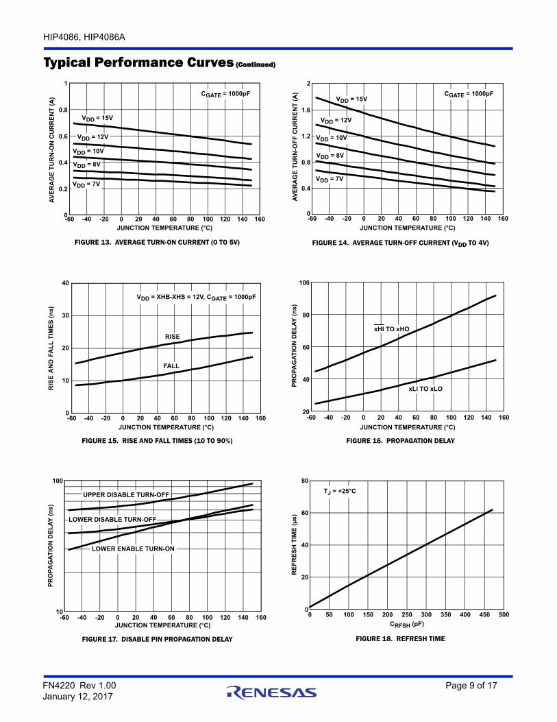
FIGURE 13. AVERAGE TURN-ON CURRENT (0 TO 5V) FIGURE 14. AVERAGE TURN-OFF CURRENT (VDD TO 4V)
FIGURE 15. RISE AND FALL TIMES (10 TO 90%) FIGURE 16. PROPAGATION DELAY
FIGURE 17. DISABLE PIN PROPAGATION DELAY FIGURE 18. REFRESH TIME
Typical Performance Curves (Continued)
-60 -40 -20 0 20 40 60 80 100 120 140 1600
0.2
0.4
0.6
0.8
1
JUNCTION TEMPERATURE (°C)
AV
ER
AG
E T
UR
N-O
N C
UR
RE
NT
(A
) CGATE = 1000pF
VDD = 15V
VDD = 8V
VDD = 10V
VDD = 12V
VDD = 7V
-60 -40 -20 0 20 40 60 80 100 120 140 1600
0.4
0.8
1.2
1.6
2
JUNCTION TEMPERATURE (°C)
AV
ER
AG
E T
UR
N-O
FF
CU
RR
EN
T (
A) CGATE = 1000pF
VDD = 15V
VDD = 8V
VDD = 10V
VDD = 12V
VDD = 7V
-60 -40 -20 0 20 40 60 80 100 120 140 1600
10
20
30
40
JUNCTION TEMPERATURE (°C)
RIS
E A
ND
FA
LL
TIM
ES
(n
s)
RISE
FALL
VDD = XHB-XHS = 12V, CGATE = 1000pF
-60 -40 -20 0 20 40 60 80 100 120 140 16020
40
60
80
100
JUNCTION TEMPERATURE (°C)
PR
OP
AG
AT
ION
DE
LA
Y (
ns
)
xHI TO xHO
xLI TO xLO
JUNCTION TEMPERATURE (°C)-60 -40 -20 0 20 40 60 80 100 120 140 160
10
100
PR
OP
AG
AT
ION
DE
LA
Y (
ns)
LOWER ENABLE TURN-ON
LOWER DISABLE TURN-OFF
UPPER DISABLE TURN-OFF
CRFSH (pF)
0 50 100 150 200 250 300 350 400 450 5000
20
40
60
80
RE
FR
ES
H T
IME
(µ
s)
TJ = +25°C
FN4220 Rev 1.00 Page 9 of 17January 12, 2017
HIP4086, HIP4086A
Functional DescriptionInput LogicNOTE: When appropriate for brevity, input and output pins will be prefixed with an “x” as a substitute for A, B, or C. For example, xHS refers to pins AHS, BHS, and CHS.
The HIP4086/A are 3-phase bridge drivers designed specifically for motor drive applications. Three identical half bridge sections, A, B and C, can be controlled individually by their input pins, ALI, AHI, BLI, BHI, and CLI, CHI (xLI, xHI) or the 2 corresponding input pins for each section can be tied together to form a PWM input (xLI connected to xHI = xPWM). When controlling individual inputs, the programmable dead time is optional but shoot-through protection must then be incorporated in the timing of the input signals. If the PWM mode is chosen, then the internal programmable dead time must be used.
Shoot-Through ProtectionDead time, to prevent shoot-through, is implemented by delaying the turn-on of the high-side and low-side drivers. The delay timers
are enabled if the voltage on the RDEL pin is greater than 100mV. The voltage on RDEL will be greater than 100mV for any value of programming resistor in the specified range. If the voltage on RDEL is less than 100mV, the delay timers are disabled and no shoot-through protection is provided by the internal logic of the HIP4086/A. When the dead time is to be disabled, RDEL should be shorted to VSS.
Refresh PulseTo insure that the boot capacitors are charged prior to turning on the high-side drivers, a refresh pulse is triggered when DIS is low or when the UV comparator transitions low (VDD is greater than the programmed undervoltage threshold). Please refer to the “Block Diagram” on page 2. When triggered, the refresh pulse turns on all of the low-side drivers (xLO = 1) and turns off all of the high-side drivers (xHO = 0) for a duration set by a resistor tied between RDEL and VSS. When xLO = 1, the low-side bridge FETs charge the boot capacitors from VDD through the boot diodes.
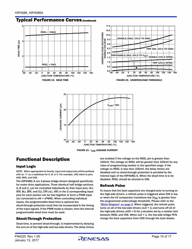
FIGURE 19. DEAD TIME FIGURE 20. UNDERVOLTAGE THRESHOLD
FIGURE 21. IxHS LEAKAGE CURRENT
Typical Performance Curves (Continued)
JUNCTION TEMPERATURE (°C)-60 -40 -20 0 20 40 60 80 100 120 140 1600
2
4
6
DE
AD
TIM
E (
µs
)
RDEL = 100kΩ
RDEL = 10kΩ
JUNCTION TEMPERATURE (°C)
UN
DE
RV
OLT
AG
E S
HU
TD
OW
N/
-60 -40 -20 0 20 40 60 80 100 120 140 1606.0
6.5
7.0
7.5
8.0
8.5
9.0
9.5
10.0
10.5
11.0
EN
AB
LE
VO
LTA
GE ENABLE (50kΩ, UVLO TO GND)
TRIP (50k, UVLO TO GND)
ENABLE (UVLO OPEN)
TRIP (UVLO OPEN)
TRIP/ENABLE (0kΩ, UVLO TO VDD)
JUNCTION TEMPERATURE (°C)-60 -40 -20 0 20 40 60 80 100 120 140 160
10
15
20
25
LE
AK
AG
E C
UR
RE
NT
(µ
A)
VxHS = 80V
FN4220 Rev 1.00 Page 10 of 17January 12, 2017

HIP4086, HIP4086A
Charge PumpThe internal charge pump of the HIP4086/A is used to maintain the bias on the boot capacitor for 100% duty cycle. There is no limit for the duration of this period. The user must understand that this charge pump is only intended to provide the static bias current of the high-side drivers and the gate leakage current of the high-side bridge FETs. It cannot provide in a reasonable time, the majority of the charge on the boot capacitor that is consumed, when the xHO drivers source the gate charge to turn on the high-side bridge FETs. The boot capacitors should be sized so that they do not discharge excessively when sourcing the gate charge. See “Application Information” for methods to size the boot capacitors.
The charge pump has sufficient capacity to source a worst-case minimum of 40µA to the external load. The gate leakage current of most power MOSFETs is about 100nA so there is more than sufficient current to maintain the charge on the boot capacitors. Because the charge pump current is small, a gate-to-source resistor on the high-side bridge FETs is not recommended. When calculating the leakage load on the outputs of xHS, also include the leakage current of the boot capacitor. This is rarely a problem but it could be an issue with electrolytic capacitors at high temperatures.
Application InformationSelecting the Boot Capacitor ValueThe boot capacitor value is chosen not only to supply the internal bias current of the high-side driver but also, and more significantly, to provide the gate charge of the driven FET without causing the boot voltage to sag excessively. In practice, the boot capacitor should have a total charge that is about 20 times the gate charge of the driven power FET for approximately a 5% drop in voltage after charge has been transferred from the boot capacitor to the gate capacitance.
The following parameters shown in Table 2 are required to calculate the value of the boot capacitor for a specific amount of voltage droop when using the HIP4086/A (no charge pump). In Table 2, the values used are arbitrary. They should be changed to comply with the actual application.
Equation 1 calculates the total charge required for the Period duration. This equation assumes that all of the parameters are constant during the Period duration. The error is insignificant if Ripple is small.
If the gate-to-source resistor is removed (RGS is usually not needed or recommended), then:
Cboot = 0.33µF
These values of Cboot will sustain the high-side driver bias during Period with only a small amount of Ripple. But in the case of the HIP4086, the charge pump reduces the value of Cboot even more. The specified charge pump current is a minimum of 40µA, which is more than sufficient to source Igate_leak. Also, because the specified charge pump current is in excess of what is needed for IHB, the total charge required to be sourced by the boot capacitor is shown by Equation 2.
Not only is the required boot capacitor smaller in value, there is no restriction on the duration of Period.
TABLE 2.
VDD = 10V VDD can be any value between 7 and 15VDC.
VHB = VDD - 0.6V = VHO
High-side driver bias voltage (VDD - boot diode voltage) referenced to VHS.
Period = 1ms This is the longest expected switching period.
IHB= 100µA Worst case high-side driver current when xHO = high (this value is specified for VDD = 12V but the error is not significant).
RGS = 100kΩ Gate-to-source resistor (usually not needed).
Ripple = 5% Desired ripple voltage on the boot capacitor (larger ripple is not recommended).
Igate_leak = 100nA From the FET vendor’s datasheet.
Qgate80V = 64nC From Figure 22.
QC Qgate80V= Period (IHB VHO RGS Igate_leak+ )+ +
(EQ. 1)
Cboot QC= RippleVDD
Cboot 0.52F=
QC Qgate80V= or Cboot 0.13F= (EQ. 2)
FIGURE 22. TYPICAL GATE VOLTAGE vs GATE CHARGE
FN4220 Rev 1.00 Page 11 of 17January 12, 2017

HIP4086, HIP4086A
Typical Application Circuit
Figure 23 is an example of how the HIP4086 and HIP4086A 3-phase drivers can be applied to drive a 3-phase motor.
Depending on the application, the switching speed of the bridge FETs can be reduced by adding series connected resistors between the xHO outputs and the FET gates. Gate-to-source resistors are recommended on the low-side FETs to prevent unexpected turn-on of the bridge should the bridge voltage be applied before VDD. Gate-to-source resistors on the high-side FETs are not usually required if low-side gate-to-source resistors are used. If relatively small gate-to-source resistors are used on the high-side FETs, be aware that they will load the charge pump of the HIP4086 negating the ability of the charge pump to keep the high-side driver biased during very long periods.
An important operating condition that is frequently overlooked by designers is the negative transient on the xHS pins that occurs when the high-side bridge FET turns off. The absolute maximum transient allowed on the xHS pin is -6V but it is wise to minimize the amplitude to lower levels. This transient is the result of the parasitic inductance of the low-side drain-to-source conductor on the PCB. Even the parasitic inductance of the low-side FET contributes to this transient.
When the high-side bridge FET turns off, because of the inductive characteristics of a motor load, the current that was flowing in
the high-side FET (blue) must rapidly commutate to flow through the low-side FET (red). The amplitude of the negative transient impressed on the xHS node is (di/dt x L) where L is the total parasitic inductance of the low-side FET drain-to-source path and di/dt is the rate at which the high-side FET is turned off. With the increasing power levels of new generation motor drives, clamping this transient becomes more and more significant for the proper operation of the HIP4086/A.
There are several ways of reducing the amplitude of this transient. If the bridge FETs are turned off more slowly to reduce di/dt, the amplitude will be reduced but at the expense of more switching losses in the FETs. Careful PCB design will also reduce the value of the parasitic inductance. However, these two solutions by themselves may not be sufficient. Figure 24 illustrates a simple method for clamping the negative transient. Two series connected, fast PN junction, 1A diodes are connected between xHS and VSS as shown. It is important that the components be placed as close as possible to the xHS and VSS pins to minimize the parasitic inductance of this current path. Two series connected diodes are required because they are in parallel with the body diode of the low-side FET. If only one diode is used for the clamp, it will conduct some of the negative load current that is flowing in the low-side FET. In severe cases, a small value resistor in series with the xHS pin as shown, will further reduce the amplitude of the negative transient.
Please note that a similar transient with a positive polarity occurs when the low-side FET turns off. This is less frequently a problem because xHS node is floating up toward the bridge bias voltage. The absolute maximum voltage rating for the xHS node does need to be observed when the positive transient occurs.
Controller
AHO
CLO
BLO
ALO
CHO
BHO
CLI
BLI
ALI
CHI
BHI
AHICHS
AHS
BHS
CHB
AHB
BHB
VDD
RDEL
VDD
Speed
Brake
Battery24V...48V
HIP
408
6/A
VSS
FIGURE 23. TYPICAL APPLICATION CIRCUIT
FIGURE 24. BRIDGE WITH PARASITIC INDUCTANCES
V S S
x H S
x L O
x H O IN D U C T IV E L O A D
+
-
+
-
FN4220 Rev 1.00 Page 12 of 17January 12, 2017

HIP4086, HIP4086A
General PCB Layout GuidelinesThe AC performance of the HIP4086/A depends significantly on the design of the PC board. The following layout design guidelines are recommended to achieve optimum performance:
• Place the driver as close as possible to the driven power FETs.
• Understand where the switching power currents flow. The high amplitude di/dt currents of the driven power FET will induce significant voltage transients on the associated traces.
• Keep power loops as short as possible by paralleling the source and return traces.
• Use planes where practical; they are usually more effective than parallel traces.
• Avoid paralleling high amplitude di/dt traces with low level signal lines. High di/dt will induce currents and consequently, noise voltages in the low level signal lines.
• When practical, minimize impedances in low level signal circuits. The noise, magnetically induced on a 10kΩ resistor, is 10x larger than the noise on a 1kΩ resistor.
• Be aware of magnetic fields emanating from motors, transformers and inductors. Gaps in these magnetic structures are especially bad for emitting flux.
• If you must have traces close to magnetic devices, align the traces so that they are parallel to the flux lines to minimize coupling.
• The use of low inductance components such as chip resistors and chip capacitors is highly recommended.
• Use decoupling capacitors to reduce the influence of parasitic inductance in the VDD and GND leads. To be effective, these
capacitors must also have the shortest possible conduction paths. If vias are used, connect several paralleled vias to reduce the inductance of the vias.
• It may be necessary to add resistance to dampen resonating parasitic circuits especially on xHO and xLO. If an external gate resistor is unacceptable, then the layout must be improved to minimize lead inductance.
• Keep high dv/dt nodes away from low level circuits. Guard banding can be used to shunt away dv/dt injected currents from sensitive circuits. This is especially true for control circuits that source the input signals to the HIP4086/A.
• Avoid having a signal ground plane under a high amplitude dv/dt circuit. This will inject di/dt currents into the signal ground paths.
• Do power dissipation and voltage drop calculations of the power traces. Many PCB/CAD programs have built in tools for calculation of trace resistance.
• Large power components (power FETs, electrolytic capacitors, power resistors, etc.) will have internal parasitic inductance which cannot be eliminated. This must be accounted for in the PCB layout and circuit design.
• If you simulate your circuits, consider including parasitic components especially parasitic lead inductance.
FN4220 Rev 1.00 Page 13 of 17January 12, 2017

HIP4086, HIP4086A
Revision History The revision history provided is for informational purposes only and is believed to be accurate, however, not warranted. Please go to the web to make sure that you have the latest revision.
DATE REVISION CHANGE
January 12, 2017 FN4220.11 The following revisions were made to the DC and AC Electrical Specifications:-VDD Quiescent Current (HIP4086): updated maximum (TJ = +25°C) from “4.2” to “5.1”, updated min and
max (TJ = -40°C to +150°C) from “2.1” to “1.96” and “4.3” to “5.3”, respectively.-VDD Quiescent Current (HIP4086A): updated max and typical (TJ = +25°C) from “2.6” to “3.1” and from “2.4”
to “2.8”, updated min and max (TJ = -40°C to +150°C) from “2.1” to “1.8” and from “2.7” to “3.3”, respectively.-VDD Operating Current (HIP4086): updated min and max (TJ = +25°C) from “6.3” to “5.4” and from “10.5”
to “13”, updated min and max (TJ = -40°C to +150°C) from “5” to “4” and “11” to 13.5”, respectively.-VDD Operating Current (HIP4086A): updated typical and max (TJ = +25°C) from “3.6” to “4.0” and from “4.1”
to “4.6”, updated min and max (TJ = -40°C to +150°C) from “2.8” to “2.7” and from “4.4” to “5.1”, respectively.-xHB On Quiescent Current (HIP4086): updated maximum (TJ = +25°C) from “80” to “110”, updated
maximum (TJ = -40°C to +150°C) from “100” to “140”.-xHB On Quiescent Current (HIP4086A): updated typical and max (TJ = +25°C) from “80” to “90” and from
“100” to “115”, updated maximum (TJ = -40°C to +150°C) from “200” to “225”.-xHB Off Quiescent Current (HIP4086A): updated typical and max (TJ = +25°C) from “0.9” to “1.0” and from
“1” to “1.2”, updated maximum (TJ = -40°C to +150°C) from “1.2” to “1.25”.-xHB Operating Current (HIP4086A): updated maximum (TJ = +25°C) from “1” to “1.1”, updated maximum
(TJ = -40°C to +150°C) from “1.2” to “1.25”.-xHB, xHS Leakage Current: updated typical (TJ = +25°C) from “24” to “30”.-Minimum Undervoltage Threshold: updated min (TJ = -40°C to +150°C) from “4.9” to “4.8”.-QPUMP Output Voltage: updated min and max (TJ = +25°C) from “11.5” to “11” and from “14” to “14.6”,
updated min and max (TJ = -40°C to +150°C) from “10.5” to “10” and “14.5” to “14.75”, respectively.-QPUMP Output Current: updated min and max (TJ = +25°C) from “50” to “40” and from “130” to “160”,
updated maximum (TJ = -40°C to +150°C) from “140” to “185”.-Low Level Input Current: updated maximum (TJ = +25°C) from “-135” to “-155”, updated maximum
(TJ = -40°C to +150°C) from “-140” to “-165”.-Low Level Output Voltage: updated maximum (TJ = -40°C to +150°C) from “200” to “210”.-Dead Time (RDEL = 100kΩ): updated min and max (TJ = +25°C) from “3.8” to “3” and from “6” to “7.2”,
updated maximum (TJ = -40°C to +150°C) from “7” to “8”.-Dead Time (RDEL = 10kΩ): updated maximum (TJ = +25°C) from “0.65” to “0.75”, updated maximum
(TJ = -40°C to +150°C) from “0.7” to “0.8”.-xLI to xLO turn-off: updated maximum (TJ = +25°C) from “45” to “55”, updated maximum
(TJ = -40°C to +150°C) from “65” to “75”.-xHI to xHO turn-off: updated maximum (TJ = +25°C) from “90” to “110”, updated maximum
(TJ = -40°C to +150°C) from “100” to “135”.-xLI to xLO turn-on: updated maximum (TJ = +25°C) from “75” to “82”, updated maximum
(TJ = -40°C to +150°C) from “90” to “100”.-xHI to xHO turn-on: updated maximum (TJ = +25°C) from “90” to “110”, updated maximum
(TJ = -40°C to +150°C) from “100” to “158”.-Rise Time: updated maximum (TJ = -40°C to +150°C) from “50” to “60”.-Fall Time: updated maximum (TJ = -40°C to +150°C) from “25” to “40”.-DIS to xLO turn-off: updated maximum (TJ = -40°C to +150°C) from “90” to “104”.-DIS to xHO turn-off: updated maximum (TJ = +25°C) from “90” to “116”, updated maximum
(TJ = -40°C to +150°C) from “100” to “147”.-DIS to xLO turn-on: updated maximum (TJ = +25°C) from “80” to “85”, updated maximum (TJ = -40°C to
+150°C) from “100” to “120”.Minor Parameter label changes to use consistent descriptions for related parameters.Updated from “50µA” to “40µA” in “Charge Pump” and “Selecting the Boot Capacitor Value” on page 11.
March 27, 2015 FN4220.10 Added AN1829, “HIP4086 3-Phase BLDC Motor Drive Demonstration Board, User Guide” bullet to the related literature section on page 1.On page 3:
In the Pin Configuration updated typo for Pin 17 Pin Name from “AHC” to “AHO”.In the Pin Description table:
Updated RDEL and UVLO Description to reference the correct Figures. RDEL - from “Figure 18” to “Figure 19” and UVLO - from “Figure 19”to “Figure 20”.
Updated typo-AHS pin number from “15” to “18”. Added “RDEL range10kΩ to 100kΩ” to the “Maximum Recommended Operating Conditions” on page 5.Updated the About Intersil verbiage.
January 28, 2013 FN4220.9 Corrected following typo in the second paragraph of page 1:From: (0.5ms to 4.5ms)To: (0.5µs to 4.5µs)
FN4220 Rev 1.00 Page 14 of 17January 12, 2017

HIP4086, HIP4086A
Intersil products are manufactured, assembled and tested utilizing ISO9001 quality systems as notedin the quality certifications found at www.intersil.com/en/support/qualandreliability.html
Intersil products are sold by description only. Intersil may modify the circuit design and/or specifications of products at any time without notice, provided that such modification does not, in Intersil's sole judgment, affect the form, fit or function of the product. Accordingly, the reader is cautioned to verify that datasheets are current before placing orders. Information furnished by Intersil is believed to be accurate and reliable. However, no responsibility is assumed by Intersil or its subsidiaries for its use; nor for any infringements of patents or other rights of third parties which may result from its use. No license is granted by implication or otherwise under any patent or patent rights of Intersil or its subsidiaries.
For information regarding Intersil Corporation and its products, see www.intersil.com
For additional products, see www.intersil.com/en/products.html
© Copyright Intersil Americas LLC 2011-2017. All Rights Reserved.All trademarks and registered trademarks are the property of their respective owners.
About IntersilIntersil Corporation is a leading provider of innovative power management and precision analog solutions. The company's products address some of the largest markets within the industrial and infrastructure, mobile computing and high-end consumer markets.
For the most updated datasheet, application notes, related documentation and related parts, please see the respective product information page found at www.intersil.com.
For a listing of definitions and abbreviations of common terms used in our documents, visit: www.intersil.com/glossary.
You may report errors or suggestions for improving this datasheet by visiting www.intersil.com/ask.
Reliability reports are also available from our website at www.intersil.com/support.
September 27, 2012 FN4220.8 Removed evaluation board from “Ordering Information” and “Related Literature” since it is inactive.
June 1, 2011 FN4220.7 Added alternate parameters for HIP4086A in DC Electrical Specifications Table Supply Currents on page 5.Added to Charge Pump Figures 11 and 12 in Typical Performance Curves “HIP4086 Only”-Converted to new Intersil datasheet template.-Changed Title from “80V, 500mA, 3-Phase Driver” to “80V, 500mA, 3-Phase MOSFET Driver”.-Rewrote description on page 1 by adding HIP4086A and stating the differences between parts.-Updated “Ordering Information” on page 4 by adding part number HIP4086AABZ and Eval Board. Added MSL note. Removed obsolete part HIP4086AP.-Updated “TYPICAL APPLICATION” on page 1.-Added Figure 2 on page 1.-Updated “Features” and “Applications” section on page 1.-Added “” on page 1.-Updated “Block Diagram” on page 2 by adding color and notes.-Updated “Thermal Information” and notes on page 5.-Added “Boldface limits apply..” to common conditions of Electrical Specifications tables. Added Note 9 to MIN and MAX columns of Electrical Specifications tables.-Updated all timing diagrams for better clarification on page 7.-Added “Functional Description”, “Application Information” and “General PCB Layout Guidelines” sections beginning on page 10.-Updated Package Outline Drawing M24.3 by removing table listing dimensions and putting dimensions on drawing. Added Land Pattern.-Added “Revision History” and “About Intersil” to page 15.
July 26, 2004 FN4220.6 Added Pb-Free parts to “Ordering Information” on page 4.
February 18, 2003 FN4220.5 Revised “Pin Descriptions” on page 3.Revised “Low Level Input Current” specs on page 6.
May, 1999 FN4220.4 Initial Release.
Revision History The revision history provided is for informational purposes only and is believed to be accurate, however, not warranted. Please go to the web to make sure that you have the latest revision. (Continued)
DATE REVISION CHANGE
FN4220 Rev 1.00 Page 15 of 17January 12, 2017
HIP4086, HIP4086A
FN4220 Rev 1.00 Page 16 of 17January 12, 2017
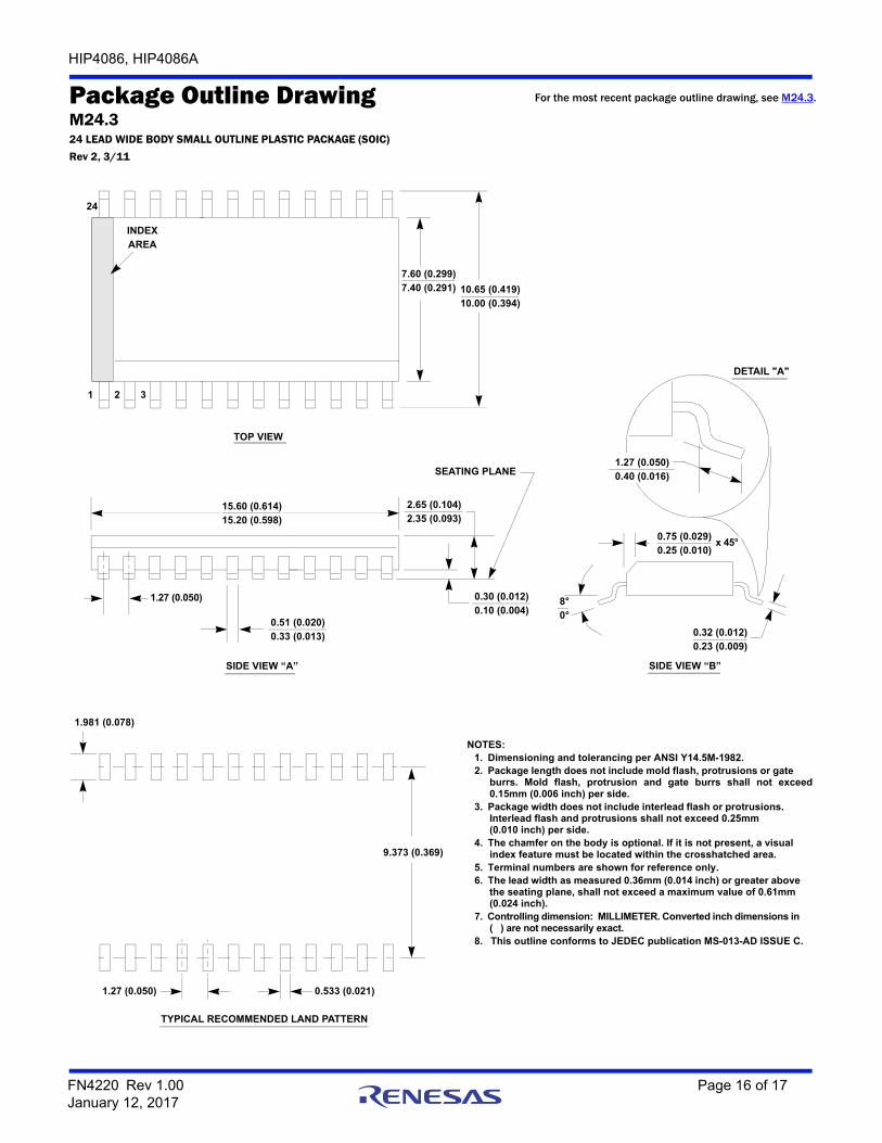
Package Outline DrawingM24.3 24 LEAD WIDE BODY SMALL OUTLINE PLASTIC PACKAGE (SOIC)
Rev 2, 3/11
TOP VIEW
NOTES:1. Dimensioning and tolerancing per ANSI Y14.5M-1982.2. Package length does not include mold flash, protrusions or gate
burrs. Mold flash, protrusion and gate burrs shall not exceed0.15mm (0.006 inch) per side.
3. Package width does not include interlead flash or protrusions. Interlead flash and protrusions shall not exceed 0.25mm (0.010 inch) per side.
4. The chamfer on the body is optional. If it is not present, a visualindex feature must be located within the crosshatched area.
5. Terminal numbers are shown for reference only.6. The lead width as measured 0.36mm (0.014 inch) or greater above
the seating plane, shall not exceed a maximum value of 0.61mm (0.024 inch).
7. Controlling dimension: MILLIMETER. Converted inch dimensions in ( ) are not necessarily exact.
8. This outline conforms to JEDEC publication MS-013-AD ISSUE C.
SIDE VIEW “A” SIDE VIEW “B”
TYPICAL RECOMMENDED LAND PATTERN
INDEXAREA
24
1 2 3
SEATING PLANE
DETAIL "A"
x 45°
7.60 (0.299)7.40 (0.291)
0.75 (0.029)0.25 (0.010)
10.65 (0.419)10.00 (0.394)
1.27 (0.050)0.40 (0.016)
15.60 (0.614)15.20 (0.598)
2.65 (0.104)2.35 (0.093)
0.30 (0.012)0.10 (0.004)
1.27 (0.050)
0.51 (0.020)0.33 (0.013) 0.32 (0.012)
0.23 (0.009)
8°0°
1.981 (0.078)
9.373 (0.369)
0.533 (0.021)1.27 (0.050)
For the most recent package outline drawing, see M24.3.

HIP4086, HIP4086A
FN4220 Rev 1.00 Page 17 of 17January 12, 2017
Dual-In-Line Plastic Packages (PDIP)
NOTES:
1. Controlling Dimensions: INCH. In case of conflict between English and Metric dimensions, the inch dimensions control.
2. Dimensioning and tolerancing per ANSI Y14.5M-1982.
3. Symbols are defined in the “MO Series Symbol List” in Section 2.2 of Publication No. 95.
4. Dimensions A, A1 and L are measured with the package seated in JEDEC seating plane gauge GS-3.
5. D, D1, and E1 dimensions do not include mold flash or protrusions. Mold flash or protrusions shall not exceed 0.010 inch (0.25mm).
6. E and are measured with the leads constrained to be perpendicular to datum .
7. eB and eC are measured at the lead tips with the leads unconstrained. eC must be zero or greater.
8. B1 maximum dimensions do not include dambar protrusions. Dambar protrusions shall not exceed 0.010 inch (0.25mm).
9. N is the maximum number of terminal positions.
10. Corner leads (1, N, N/2 and N/2 + 1) for E8.3, E16.3, E18.3, E28.3, E42.6 will have a B1 dimension of 0.030 - 0.045 inch (0.76 - 1.14mm).
eA-C-
CL
E
eA
C
eB
eC
-B-
E1INDEX
1 2 3 N/2
N
AREA
SEATING
BASEPLANE
PLANE
-C-
D1
B1B
e
D
D1
AA2
L
A1
-A-
0.010 (0.25) C AM B S
E24.3 (JEDEC MS-001-AF ISSUE D)
24 LEAD NARROW BODY DUAL-IN-LINE PLASTIC PACKAGE
SYMBOL
INCHES MILLIMETERS
NOTESMIN MAX MIN MAX
A - 0.210 - 5.33 4
A1 0.015 - 0.39 - 4
A2 0.115 0.195 2.93 4.95 -
B 0.014 0.022 0.356 0.558 -
B1 0.045 0.070 1.15 1.77 8
C 0.008 0.014 0.204 0.355 -
D 1.230 1.280 31.24 32.51 5
D1 0.005 - 0.13 - 5
E 0.300 0.325 7.62 8.25 6
E1 0.240 0.280 6.10 7.11 5
e 0.100 BSC 2.54 BSC -
eA 0.300 BSC 7.62 BSC 6
eB - 0.430 - 10.92 7
L 0.115 0.150 2.93 3.81 4
N 24 24 9
Rev. 0 12/93
For the most recent package outline drawing, see E24.3.