host-guest s elf-assembly in block copolymer blends
TRANSCRIPT

Host-Guest Self-assembly in Block Copolymer Blends
The MIT Faculty has made this article openly available. Please share how this access benefits you. Your story matters.
Citation Park, Woon Ik, YongJoo Kim, Jae Won Jeong, Kyungho Kim, Jung-Keun Yoo, Yoon Hyung Hur, Jong Min Kim, Edwin L. Thomas, AlfredoAlexander-Katz, and Yeon Sik Jung. “Host-Guest Self-assembly inBlock Copolymer Blends.” Scientific Reports 3 (November 12, 2013).
As Published http://dx.doi.org/10.1038/srep03190
Publisher Nature Publishing Group
Version Final published version
Citable link http://hdl.handle.net/1721.1/85012
Detailed Terms http://creativecommons.org/licenses/by-nc-sa/3.0/
Host-Guest Self-assembly in BlockCopolymer BlendsWoon Ik Park1, YongJoo Kim2, Jae Won Jeong1, Kyungho Kim1, Jung-Keun Yoo1, Yoon Hyung Hur1,Jong Min Kim1, Edwin L. Thomas3, Alfredo Alexander-Katz2 & Yeon Sik Jung1
1Department of Materials Science and Engineering, Korea Advanced Institute of Science and Technology (KAIST), 291 Daehak-ro,Yuseong-gu, Daejeon 305-701, Republic of Korea, 2Department of Materials Science and Engineering, Massachusetts Institute ofTechnology (MIT), Cambridge, MA 02139, USA, 3Department of Mechanical Engineering & Materials Science, Rice University,Houston, TX 77005, USA.
Ultrafine, uniform nanostructures with excellent functionalities can be formed by self-assembly of blockcopolymer (BCP) thin films. However, extension of their geometric variability is not straightforward due totheir limited thin film morphologies. Here, we report that unusual and spontaneous positioning betweenhost and guest BCP microdomains, even in the absence of H-bond linkages, can create hybridizedmorphologies that cannot be formed from a neat BCP. Our self-consistent field theory (SCFT) simulationresults theoretically support that the precise registration of a spherical BCP microdomain (guest, B-b-C) atthe center of a perforated lamellar BCP nanostructure (host, A-b-B) can energetically stabilize the blendedmorphology. As an exemplary application of the hybrid nanotemplate, a nanoring-type Ge2Sb2Te5 (GST)phase-change memory device with an extremely low switching current is demonstrated. These resultssuggest the possibility of a new pathway to construct more diverse and complex nanostructures usingcontrolled blending of various BCPs.
For the last several decades, self-assembled block copolymer (BCP) thin films have been extensively studiedfor applications involving the generation of functional nanostructures1–4. Moreover, excellent pattern reso-lution (5 – 20 nm), cost-effectiveness, and scalability of directed self-assembly (DSA) based on BCPs suggest
that this is a practical method to complement optical lithography5–19. However, extension of the available suite ofgeometries has been one of the critical challenges in the applications of those functional nanostructures becausepure diblock copolymer (di-BCP) thin films present restricted sets of self-assembled morphologies such asspheres, cylinders, gyroids and lamellae12. Various innovative approaches have recently been suggested as poten-tial solutions. For example, non-regular patterns with a wide range of geometric variability were demonstratedusing 2-dimensional (2D) dense guiding templates based on electron beam lithography20,21. Novel thin filmmicrodomain structures formed by A-B-C triblock copolymers have also been explored22,23. In addition, BCPdouble patterning can lead to the formation of hierarchical nanostructures24.
The blending of BCPs has also been widely investigated due to the advantages of simplicity and far moreextensive geometric ranges. A rich phase behavior with interesting bulk morphologies was already reported byprevious studies25–31. The governing parameters such as blend composition, volume fraction and molecularweight of each polymer component, and the Flory-Huggins segmental interaction parameter (x) have also beenextensively studied25,27,29. However, the frequent occurrence of macroscopic phase-separation between two di-BCPs often makes it difficult to achieve new and morphologically uniform nanostructures. One general criterionbased on the minimization of interfacial energy to ensure uniform microphase separation in blends of A-B and A-C BCPs is that the x between the B and C (xBC) blocks must be smaller than that between A and B (xAB) andbetween A and C (xAC), respectively25,26,29. In addition to considerations related to x, the other key parametersmentioned above also need to be precisely optimized in order to prevent macrophase-separation betweenconstituent BCPs. These strict requirements result in a very narrow process window for the formation of uniformmicrophase-separated morphologies at the nanoscale27.
In this article, we show how to effectively promote the formation of novel, uniformly microphase-separatedthin film morphologies from A-B/B-C BCP blends via host-guest self-assembly mechanism. For example, ahexagonally perforated lamellar (HPL) microdomain (host) formed by an A-B BCP can spontaneously accom-modate spherical morphology (guest) made from a B-C BCP, generating ring-shaped nanotemplates. Theminimization of free energy by the position-specific incorporation of spherical nano-spheres at the center of
OPEN
SUBJECT AREAS:NANOSCALE MATERIALS
POLYMERS
MOLECULAR SELF-ASSEMBLY
Received28 August 2013
Accepted22 October 2013
Published12 November 2013
Correspondence andrequests for materials
should be addressed toY.S.J. (ysjung@kaist.
ac.kr)
SCIENTIFIC REPORTS | 3 : 3190 | DOI: 10.1038/srep03190 1
the perforations in the HPL structure is theoretically supported byself-consistent field theory (SCFT). Furthermore, we show theformation of a ring-type hollow Ge2Sb2Te5 (GST) phase-changememory device with an extremely low switching current using theblended morphology as a practical nanotemplate.
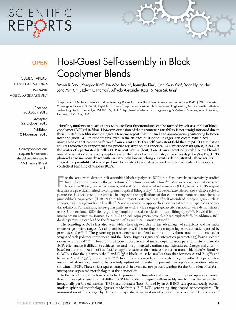
ResultsFigure 1 schematically conceptualizes an example of such hybridnanostructures: hexagonally perforated lamellae (HPL) of one di-BCP (A-b-B) combined with the spherical microdomains of anotherdi-BCP (B-b-C). The compositional choice was designed for thefabrication of nanoscale ring geometries, and the complex nano-structures can be realized by selectively removing the B polymerand reversing the remaining features comprised of the A and Cblocks. It should be noted that such complex nanostructures cannotbe prepared from a single di-BCP12,32,33. In order to fabricate thedesigned nanostructures, we chose poly(dimethylsiloxane-b-styr-ene) (PDMS-b-PS) and poly(styrene-b-ferrocenyldimethylsilane)
(PS-b-PFS) di-BCPs, where the pure organic PS (block B) are readilyselectively removed and the inorganic-containing PDMS (block A)and PFS (block C) can be oxidized to form robust inorganic nano-structures that can subsequently serve as a high-resolution etch maskas well as a removable template for the formation of functionalnanostructures.
As we demonstrated in our previous study34,35, an unusual degreeof geometrical tunability of BCP patterns can be achieved through anannealing treatment with mixed vapors composed of preferentiallyswelling solvent molecules. For PDMS-b-PS (DS45), with a molecu-
lar weight of 45.5 kg/mol and a minority volume fraction of f dryPDMS 5
33.7% in the dry state, the sample morphologies showed significantvariation depending on the ratio between heptane and toluene usedfor the solvent-annealing of the BCP, because heptane preferentiallyswells the PDMS block. Morphological transitions are due to select-ive swelling of PDMS by heptane and a consequent increase in its
effective volume fraction of PDMS (f effPDMS) during solvent anneal-
ing34. After the completion of the solvent vapor treatment, the rapid
Figure 1 | Host-guest self-assembly of blended BCPs. The chemical structures of the PDMS-b-PS and PS-b-PFS diblock copolymers (di-BCPs) used for
the self-assembly is shown. The schematics of the as-spun and self-assembled morphologies of the blended BCPs are also presented. A mixed solvent vapor
of heptane and toluene induces the formation of a perforated lamellar morphology of PDMS-b-PS that can precisely accommodate the spherical
morphology of PS-b-PFS because heptane is selectively segregated in the PDMS blocks, whereas toluene swells PS and PFS blocks more preferentially. An
inorganic dots-in-holes nanostructure is produced by oxidation of the hierarchically assembled BCP microdomains. Plasma oxidation selectively
removes the PS, while oxidizing PDMS and PFS into stable inorganic materials. The array of metallic nanorings can be obtained from pattern-reversal of
the dots-in-holes nanostructure.
www.nature.com/scientificreports
SCIENTIFIC REPORTS | 3 : 3190 | DOI: 10.1038/srep03190 2
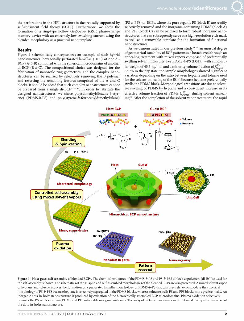
removal of solvent molecules from the BCP samples quenches in-plane morphologies36, due to predominant out-of-plane shrinkage ofthe film thickness and due to the rise of the effective glass transitiontemperature (Tg) of the matrix PS block above room temperature. Allthe solvent vapor treatments in this study were performed at 85uC foraccelerated self-assembly37. The morphologies were observed usingelectron microscopy after subjecting the BCP samples to a two-stepsequential CF4 plasma and oxygen plasma treatment process toremove the thin PDMS top layer and PS matrix, respectively38. Asshown in Figure 2a, the pure PDMS-b-PS BCP presented cylindricaland HPL morphologies when treated with vapors of pure toluene anda 151 mixture of heptane and toluene, respectively. In the HPL (orlamellar catenoid structure)39, the minority block (PDMS) forms alamellar sheet with well-aligned PS perforations having overall six-fold symmetry. Uniform thru-pores were generated by the removalof the PS domains, as can be seen in the SEM image (Figure 2a, top-middle). The average pore diameter and center-to-center distancewere 36 and 58 nm, respectively. In contrast, the morphologies ofPS-b-PFS (SF35), with a molecular weight of 35 kg/mol and a minor-
ity volume fraction of f dryPFS 5 11.5%, did not present any noticeable
change by varying the fraction of heptane in the treatment vapor, as
shown in Figure 2a (bottom). This can be attributed to the smalldifference in the solubility parameters between PS and PFS40,41, whichmay induce almost symmetric swelling for the two constituentblocks, thereby preserving the morphology regardless of the treat-ment conditions. These results on the respective di-BCPs suggest that
the effective volume fraction of PDMS (f dryPDMS) can be selectively
tunable in the blends of PDMS-b-PS and PS-b-PFS via the controlledincorporation of a preferential solvent (heptane).
As expected, simple mixtures of DS45 and SF35 treated with puretoluene vapor did not present uniformly assembled morphologies inany composition ranges. Based on the solubility parameters of PS (d5 18.5), PDMS (d 5 15.5), and PFS (d 5 18.6)40,41, the relationxPDMS/PFS $ xPDMS/PS ? xPS/PFS is obtained, and thus spatially nonuni-form microphase separation occurs due to the strong incompatibilitybetween the two BCPs. Indeed, all the blend samples with a relativemixing ratio of VDS455VSF35 5 151 to 351 showed local regions withcylindrical PDMS domains in PS and other regions of spherical PFSdomains in PS (as presented in Figure S1), confirming the macro-phase separation prediction based on x parameters. As opposed tothe PDMS cylindrical morphology shown in Figure 2a, in the 151blend (Figure S1), the PDMS forms spherical microdomains because
Figure 2 | Self-assembled morphologies of pure BCPs and blended BCPs treated by various mixed solvent vapors. (a) Morphologies of single-
component PDMS-b-PS (DS45) and PS-b-PFS (SF35) in response to different solvent vapors. Cylindrical (top-left), hexagonally perforated lamellar (top-
center), and lamellar (top-right) morphologies were obtained from the same PDMS-b-PS BCP by changing the volume ratio of heptane (VHep) and
toluene (VTol). PS-b-PFS maintained the same spherical morphology (bottom) for the different solvent vapor treatment conditions. (b) Morphological
variation of the BCP blends (PDMS-b-PS and PS-b-PFS) treated by mixed solvent vapors. The BCP blending ratio (VDS45/VSF35) was fixed at 2.5. Uniform
host-guest assembly between the two BCPs were achieved at VHep/VTol 5 1.2.
www.nature.com/scientificreports
SCIENTIFIC REPORTS | 3 : 3190 | DOI: 10.1038/srep03190 3
of the overall decrease of f effPDMS in the blend. As the fraction of DS45
in the blends increases, PDMS microdomains gradually transformedinto short cylinders (Figure S1). However, well-ordered microphase-separated morphologies were not obtained for any blending ratiowhen treated with pure toluene vapor. In addition, thermal annealingalso did not induce an ordered morphology of the blend, as shown inFigure S2.
We now demonstrate how mediation by mixed solvent vapors canlead to a new uniform microdomain pattern formed by the host-guest self-assembly of the nominally highly incompatible pair ofBCPs. Figure 2b shows how the morphology depends on the volu-metric mixture ratio of heptane and toluene (Vhep/Vtol) in the mixedsolvent vapors, while the volume ratio of DS45 and SF35 BCPs was
fixed at 2.5. With a small amount of heptane added to increase f effPDMS
in the blend, the PDMS cylinders formed a partial network structure(Figure 2b, Vhep/Vtol 5 0.33), similar to the mixed morphology ofcylinders and perforated lamellae. The expansion of the PDMS blockby heptane is supported by a gradual increase of the PDMS areafraction and a decrease of average area per PS perforation withincreasing Vhep/Vtol, as shown in Figure 4b. When Vhep/Vtol , 0.5,the PDMS network structures became more connected and continu-ous, and multiple PFS dots were isolated as a group inside the net-work. Further increase of the heptane fraction resulted in morecircular and regular perforations with reduced average diameters,although the variation in the shape and size of the perforationsresulted in a variation in the number of PFS spheres per pore.
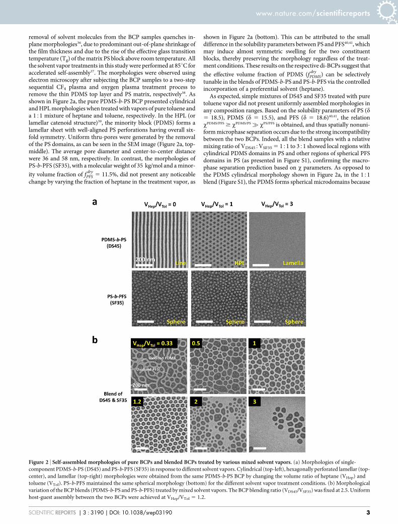
However, further tuning of Vhep/Vtol to approximately 1.2 inducedthe formation of uniform PS perforations. With the optimized vaportreatment conditions, one-to-one matched host-guest assemblybetween a PS perforation and a PFS sphere was obtained with max-imized pore number density, as presented in Figure 2b (bottom-left),Figure 3a, and Figure 4a. Atomic force microscopy (AFM) and trans-mission electron microscopy (TEM) images in Figures 3b–3d show thewell-defined morphology of the binary BCP blend. Elemental mappingof Fe (Figure 3d, center) and O (Figure 3d, right) confirm that the innerdomains are the PFS block. Additional TEM analysis and elementalmapping results are provided in Figures S3 and S4. At the optimizedprocessing conditions, small pores without a central PFS domain weredetected at a small fraction (, 4%). Most of the empty pores, with fiveneighboring pores, were observed at a tilt grain boundary where twopore lattices meet, as shown in Figure S5. This phenomenon is similarto the formation of considerably smaller central cylinders in the case ofa pentagonal arrangement compared to a hexagonal arrangement in acylinder-forming BCP42. This suggests that the spatial constraintimposed on such pores with five neighboring pores may suppressthe inclusion of spherical microdomains inside the pores. The removalof the grain boundary and the achievement of long-range orderingusing guiding templates are thus expected to eliminate the defects.
It should also be noted that there was a significant increase of poresize and pore-to-pore distance by the incorporation of the sphericalPFS microdomains in the PS perforations. The average pore diameterand periodicity with Vhep/Vtol , 1.2 were 65 nm and 82 nm, which
Figure 3 | SEM and TEM images of the host-guest self-assembly nanostructures. (a) A lower-magnification SEM image of the optimized hierarchical
morphology. (b) AFM image. (c) – (d) cross-sectional (c) and top-down (d, left) TEM images. EDS elemental mapping results for Fe (d, center) and O (d,
right). (d, center) The elemental map is overlapped with a dark field TEM image.
www.nature.com/scientificreports
SCIENTIFIC REPORTS | 3 : 3190 | DOI: 10.1038/srep03190 4
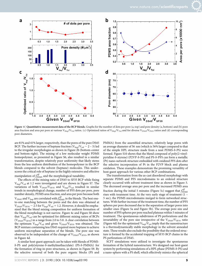
are 81% and 41% larger, respectively, than the pores of the pure DS45BCP. The further increase of heptane fraction (Vhep/Vtol , 2 – 3) ledto the irregular morphologies as shown in Figure 2b (bottom-centerand bottom-right). The mixing of a low molecular weight PDMShomopolymer, as presented in Figure S6, also resulted in a similartransformation, despite relatively poor uniformity that likely stemsfrom the less uniform distribution of the homopolymer in the BCPblends compared to the solvent (heptane) molecules. This under-scores the critical role of heptane in the highly extensive and effective
manipulation of f effPDMS and the morphological tunability.
The effects of the mixing ratio of DS45 to SF35 BCP while fixingVhep/Vtol at 1.2 were investigated and are shown in Figure S7. Thevariations of both VDS45/VSF35 and Vhep/Vtol resulted in similartrends in morphological change, number of PFS dots per pore, porenumber density, PDMS area fraction, and area per pore because both
VDS45 and Vhep are correlated with f effPDMS in the blends. The best one-
to-one matching between the pores and the dots was obtained atVDS45/VSF35 , 2.5 for Vhep/Vtol 5 1.2. However, it should be empha-sized that the blend mixing composition for uniform formation ofthe blend morphology is not narrow. Figure 4c and Figure S8 showthat Vhep/Vtol can be optimized for different mixing ratios of BCPs(VDS45/VSF35) in a range from 2.0 to 5.0. A clear correlation betweenthe optimum Vhep/Vtol and given VDS45/VSF35 was obtained. TheBCP mixture containing less DS45 required more heptane to achieveuniform microphase separation of the blends. The pore size wasobserved to be independent of the change of VDS45/VSF35, as shownin Figure 4d.
A similar host-guest approach can be taken with blends of PDMS-b-PS and poly(styrene-b-methylmethacrylate) (PS-b-PMMA) forthe formation of ring-in-pore structures, as shown in Figure S9. Bythe selective removal of both the pure organic blocks (PS and
PMMA) from the assembled structure, relatively large pores withan average diameter of 56 nm (which is 56% larger compared to thatof the simple HPL structure made from a neat PDMS-b-PS) wereformed. Figure S10 shows that the blend composed of poly(2-vinyl-pyridine-b-styrene) (P2VP-b-PS) and PS-b-PFS can form a metallic(Pt) nano-network structure embedded with oxidized PFS dots afterthe selective incorporation of Pt in the P2VP block and plasmaoxidation. These examples demonstrate the promising versatility ofhost-guest approach for various other BCP combinations.
The transformation from the as-cast disordered morphology withseparate PDMS and PFS microdomains to an ordered structureclearly occurred with solvent treatment time as shown in Figure 5.The decreased average area per pore and the increased PDMS area
fraction during the initial 5 minutes (Figure 5c) suggest that f effPDMS
rises with treatment time. At the very early stage of treatment (1 –5 sec), the PDMS microdomains merged to form networked struc-tures. With further increase of the treatment time, the number of PFSspheres per pore decreased due to the separation of larger pores intosmaller ones (Figure 5a and Figure 5b). The average pore size andnumber of PFS spheres per pore reached plateaus within 5 minutes oftreatment. The spontaneous subdivision of PS perforations and theinvariability of the pore size irrespective of the VDS45/VSF35 ratio(Figure 4d) for the optimized Vhep/Vtol imply that the nanostructureis a thermodynamically stable morphology in the solvent annealedstate. These results also exclude the possibility that the ordered struc-ture is formed by the accidental trapping of SF35 BCP chains in thePS perforations of DS45.
SCFT simulations were utilized to investigate the spontaneousformation of the hybrid nanostructure. We designed our host-guestsystem by performing simulations of a HPL phase (PDMS-b-PS) anda nano-sphere with a PS shell, which effectively mimics the spherical
Figure 4 | Quantitative measurement data of the BCP blends. Graphs for the number of dots per pore (a, top) and pore density (a, bottom) and (b) pore
area fraction and area per pore at various VHep/VTol ratios. (c) Optimized ratios of VHep/VTol and for diverse VDS45/VFS35 ratios and (d) corresponding
pore diameters.
www.nature.com/scientificreports
SCIENTIFIC REPORTS | 3 : 3190 | DOI: 10.1038/srep03190 5

nature of the PS-b-PFS corona. The unit cell of the hierarchicallyassembled structure obtained by the simulations was consistent withthe cross-sectional TEM image of the sample before plasma oxida-tion, as seen in Figures 6a and 6b. Previous hybrid-SCFT simulations,employed to study the effects of complex geometries on BCP systemscontaining defects and nano-spheres [Kim, Y., Chen, H. &Alexander-Katz, A. Unpublished data], revealed that the system isstabilized when a nano-sphere is positioned at a defect center byminimizing the chain stretching of the host BCP. Figure 6c showsthe free energy of the perforated lamellar phase of the PDMS-b-PSBCP as a function of the nano-sphere size and the position along thez-axis. For smaller nano-spheres (radius , 0.2 L0), the free energyminimization is achieved when the spheres are located at the junc-tions (Z , 6 0.2 L0) of the PS-lamellar plane and PS-perforation.However, when the radii of the nano-spheres are increased above0.2 L0, the nano-spheres eventually stabilize the system at the centerof the PS-perforations (Z 5 0) because larger nano-spheres canreduce PS chain stretching simultaneously at the upper and lowerjunctions, resulting in the minimum free energy at Z 5 0, as shown in
Figure 6c. The estimated radius of the PS-b-PFS nano-sphere of theSF35 BCP in the experiment is 0.216 L0 (,17.7 nm), which is con-sistent with the size that stabilizes the BCP blend system at Z 5 0 inthe SCFT calculation.
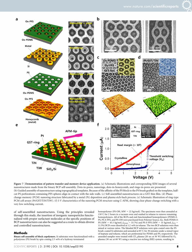
Figure 7a provides a set of the nanoscale geometries that can beobtained through the binary assembly and pattern transfer processes.Structures of dots-in-pores, nanorings, rings-in-pores, and dots-in-honeycomb are demonstrated in Figure 7a with corresponding SEMimages. The assembly of these nanostructures can be guided by topo-graphic templates, which control the position and orientation of themicrodomain lattice, as presented in Figure 7b. These patterns canalso be exploited as useful templates for making functional nano-structures. As an example, Ge2Sb2Te5 (GST) nanorings were fabri-cated by forming self-assembled structures on GST films (Figure 7c)followed by the use of a Damascene-like pattern reversal process,which was described in detail in Figure S12 and our previousreport43. Figure 7d and 7e illustrate a phase-change memory(PCM) cell array with a Pt/GST/TiN nanoring stacking structurewith outer and inner diameters of 45 nm and 20 nm, respectively.
Figure 5 | Time evolution of the self-assembled morphology. (a) SEM images of samples treated for various annealing times. Due to the use of
solvothermal treatment at 85uC, the morphological transition occurred rapidly. (b) Schematic representation of morphological development, showing
that the PS pores containing multiple PFS dots are spontaneously split into one-to-one matched microdomain structures. (c) Average pore-area (blue)
and PDMS area fraction (red) as a function of annealing time.
www.nature.com/scientificreports
SCIENTIFIC REPORTS | 3 : 3190 | DOI: 10.1038/srep03190 6

For measurement of the current-voltage (I-V) characteristics, aconductive atomic force microscope (C-AFM) tip with a radiusof 30 nm was used. The results show a clear switching behaviorfrom a high-resistance (amorphous) to a low-resistance (crystal-line) state at a threshold voltage of about 3.0 V with a sufficientsensing window (.103 at a read voltage of 2.5 V) (Figure 7f). It isnoteworthy that these nanoscale GST rings have a very lowswitching current of approximately 2 mA, which is close to thelowest programming current ever reported for nanostructures44.This is attributed to the hollow nature combined with the smalldimension of the GST nanorings, which significantly shrinks theirswitching volumes. The nanoring geometry can also be used forthe fabrication of multi-bit-storage magnetic memory elements45,46
without relying on high-resolution templates. Moreover, the sub-oxide nanostructures directly prepared from inorganic-containingBCPs without employing pattern-transfer processes can be appliedto high-density resistive memory applications, as we reportedpreviously47. This simple demonstration shows the promise ofbinary BCP blend nanostructures as useful lithographic templatesfor the fabrication of ordered functional nanostructures.
DiscussionThe uniform assembly of highly incompatible A-B/B-C di-BCPblends was shown to form useful hybrid nanotemplates by preciselytuning the volume fractions of constituent polymer blocks for con-trolled insertion of a guest BCP microdomain into a host BCPnanostructure. Our SCFT simulations as well as the experimentallyobserved morphological evolution of the BCP blends suggest that theposition-specific incorporation of the guest microdomain energet-ically stabilizes the host BCP nanostructure. This methodology issignificant in that uniform microphase separation between twoBCPs was obtained and it may allow the generation of diverse andcomplex self-assembly architectures. The host-guest self-assemblycombined with pattern reversal enabled the formation of unusualring-shape nanostructures including hollow phase-change memorynanostructures.
Furthermore, we anticipate the realization of other combinatorialmorphologies such as nanoscale line patterns with regularly chan-ging widths or alternatingly occurring dots and line patterns throughthe one-step binary assembly of various BCPs precisely manipulatedby controlled solvent vapor treatment. This will extend the geometry
Figure 6 | SCFT simulation. (a) Cross-section TEM image of the host-gest assembled BCP blend. (b) Unit cell structure for the SCFT calculation,
which is consistent with the TEM image. (c) Calculated free energy of the PDMS-b-PS HPL morphology depending on the position and size of the guest
PS-b-PFS nano-sphere incorporated in the PS perforation. For the particle radius of 0.2 – 0. 22 L0, the minimization of free energy is achieved by the
location of nano-sphere at the center. (d) The illustration of periodic configurations achieving the minimum free energy.
www.nature.com/scientificreports
SCIENTIFIC REPORTS | 3 : 3190 | DOI: 10.1038/srep03190 7
of self-assembled nanostructures. Using the principles revealedthrough this study, the insertion of inorganic nanoparticles functio-nalized with proper surfactant molecules at the specific positions ofBCP nanostructures can also be suggested as a route to obtain diverseand controlled nanostructures.
MethodsBinary self-assembly of block copolymers. Si substrates were functionalized with apolystyrene (PS) brush by spin-coating 2.5 wt% of a hydroxy-terminated
homopolymer (PS-OH, MW 5 22 kg/mol). The specimens were then annealed at150uC for 2 hours in a vacuum oven and washed in toluene to remove remaininghomopolymers. All of the BCPs and end-functionalized homopolymers (PDMS-b-PS, PS-b-PFS, and PS-OH were purchased from Polymer Source, Inc. Both PDMS-b-PS (MW 5 45.5 kg/mol, fPDMS 5 33.7%) and PS-b-PFS (MW 5 35 kg/mol, fPFS 5
11.5%) BCPs were dissolved at 1.2 wt% in toluene. The two BCP solutions were thenmixed at various ratios. The blended BCP solutions were spin-coated onto the PSbrush-coated Si substrates and annealed at 85uC for 30 minutes under a mixed vaporof heptane and toluene, which are preferential for PDMS and PS, respectively. Theannealed samples were treated with CF4 plasma (20 sec at 50 W) followed by O2
plasma (30 sec at 60 W) using a reactive ion etching (RIE) system, resulting in
Figure 7 | Demonstration of pattern transfer and memory device application. (a) Schematic illustrations and corresponding SEM images of several
nanostructures made from the binary BCP self-assembly. Dots-in-pores, nanorings, dots-in-honeycomb, and rings-in-pores are presented.
(b) Guided assembly of nanostructure using topographical templates. Because of the affinity of the PS block to the PS brush grafted on the templates, half-
cut PS perforations containing PFS spheres align in contact with the side-walls. (c) Self-assembled nanostructures on a GST thin film. (d) Phase-
change memory (PCM) nanoring structure fabricated by a metal (Pt) deposition and plasma etch-back process. (e) Schematic illustration of ring-type
PCM cell arrays (Pt/GST/TiN/TiW). (f) I-V characteristics of the nanoring PCM structure using C-AFM, showing clear phase-change switching with a
very low switching current.
www.nature.com/scientificreports
SCIENTIFIC REPORTS | 3 : 3190 | DOI: 10.1038/srep03190 8
complete removal of PS, oxidized PDMS and PFS nanostructures. Cross-sectionaland top-view TEM samples were prepared by mechanical polishing followed by ionmilling with Ar ions. TEM studies were performed using a JEOL JEM-ARM200Fmicroscope with energy dispersive X-ray spectroscopy (EDS) operated at 200 kV.
Fabrication of phase-change nanostructures and measurements. Si wafers with athermally-grown SiO2 layer (200 nm) were used as substrates. The bottom electrodeTiW (150 nm), heater TiN (100 nm), and phase-change material Ge2Sb2Te5
(20 nm) were deposited by radio-frequency (RF) sputtering. Pt was sputter-depositedonto the self-assembled nanostructures and then back-etched by CF4 and Cl2 plasmaat 200 W for 2 minutes. To obtain the final GST ring nanostructures, the GST filmwas patterned using CF4 plasma and Pt nanoring patterns as an etch-mask. Theresistive switching behaviors for PCM cell arrays were characterized by using aconductive atomic force microscope (C-AFM, SPA 400, Seiko) with a Pt-coated AFMtip (EFM tips, Nanosensors). While the bottom electrodes (TiW) were grounded, abias voltage was swept over the top electrode (Pt) from 0 to 5 V with a step size of0.01 V.
Self-consistent field theory (SCFT) simulations. We simulated the host blockcopolymer (perforated lamellar phase) and guest block copolymer (nano-sphereattracted to majority block) by utilizing a hybrid particle-field simulation, developedby Fredrickson and co-workers48. To obtain the perforated lamellar phase, the gyroidphase (f 5 0.675, xN 5 20) of the block copolymer was compressed to thin films withthicknesses comparable to the experiment. The top PDMS brush and bottom PSbrush successfully mimicked the experimental PDMS-air interface and Si substrate.To simulate the spherical PS-PFS phase, a nano-sphere with an affinity for the PSblocks and a Gaussian cavity function for the density field of nano-sphere wasinserted. Simulations were performed using the newly developed graphics processingunit (GPU) optimized Lattice-Boltzmann diffusion-equation solver49.
1. Thurn-Albrecht, T. et al. Ultrahigh-Density Nanowire Arrays Grown in Self-Assembled Diblock Copolymer Templates. Science 290, 2126–2129 (2000).
2. Cheng, J. Y. et al. Formation of a Cobalt Magnetic Dot Array via Block CopolymerLithography. Adv. Mater. 13, 1174–1178 (2001).
3. Warren, S. C. et al. Ordered Mesoporous Materials from Metal Nanoparticle–Block Copolymer Self-Assembly. Science 320, 1748–1752 (2008).
4. Zhao, Y. et al. Small-molecule-directed nanoparticle assembly towards stimuli-responsive nanocomposites. Nat. Mater. 8, 979–985 (2009).
5. Park, M., Harrison, C., Chaikin, P. M., Register, R. A. & Adamson, D. H. Blockcopolymer lithography: Periodic arrays of similar to 1011 holes in 1 squarecentimeter. Science 276, 1401–1404 (1997).
6. Segalman, R. A., Yokoyama, H. & Kramer, E. J. Graphoepitaxy of sphericaldomain block copolymer films. Adv. Mater. 13, 1152–1155 (2001).
7. Kim, S. O. et al. Epitaxial self-assembly of block copolymers on lithographicallydefined nanopatterned substrates. Nature 424, 411–414 (2003).
8. Cheng, J. Y., Mayes, A. M. & Ross, C. A. Nanostructure engineering by templatedself-assembly of block copolymers. Nat. Mater. 3, 823–828 (2004).
9. Cheng, J. Y., Ross, C. A., Smith, H. I. & Thomas, E. L. Templated self-assembly ofblock copolymers: Top-down helps bottom-up. Adv. Mater. 18, 2505–2521(2006).
10. Stoykovich, M. P. et al. Directed assembly of block copolymer blends intononregular device-oriented structures. Science 308, 1442–1446 (2005).
11. Chai, J., Wang, D., Fan, X. N. & Buriak, J. M. Assembly of aligned linear metallicpatterns on silicon. Nat. Nanotechnol. 2, 500–506 (2007).
12. Black, C. T. et al. Polymer self assembly in semiconductor microelectronics. IBMJournal of Research and Development 51, 605–633 (2007).
13. Darling, S. B. Directing the self-assembly of block copolymers. Progress in PolymerScience 32, 1152–1204 (2007).
14. Bita, I. et al. Graphoepitaxy of self-assembled block copolymers on two-dimensional periodic patterned templates. Science 321, 939–943 (2008).
15. Ruiz, R. et al. Density multiplication and improved lithography by directed blockcopolymer assembly. Science 321, 936–939 (2008).
16. Jeong, S. J. et al. Soft Graphoepitaxy of Block Copolymer Assembly withDisposable Photoresist Confinement. Nano Lett. 9, 2300–2305 (2009).
17. Tavakkoli, K. G. A. et al. Templating Three-Dimensional Self-AssembledStructures in Bilayer Block Copolymer Films. Science 336, 1294–1298 (2012).
18. Bates, C. M. et al. Polarity-Switching Top Coats Enable Orientation of Sub–10-nmBlock Copolymer Domains. Science 338, 775–779 (2012).
19. Jeong, J. W. et al. Nanotransfer Printing with sub-10 nm Resolution Realizedusing Directed Self-Assembly. Adv. Mater. 24, 3526–3531 (2012).
20. Stoykovich, M. P. et al. Directed self-assembly of block copolymers fornanolithography: Fabrication of isolated features and essential integrated circuitgeometries. ACS Nano 1, 168–175 (2007).
21. Yang, J. K. W. et al. Complex self-assembled patterns using sparse commensuratetemplates with locally varying motifs. Nat. Nanotechnol. 5, 256–260 (2010).
22. Chuang, V. P., Gwyther, J., Mickiewicz, R. A., Manners, I. & Ross, C. A. TemplatedSelf-Assembly of Square Symmetry Arrays from an ABC Triblock Terpolymer.Nano Lett. 9, 4364–4369 (2009).
23. Chuang, V. P., Ross, C. A., Bilalis, P. & Hadjichristidis, N. Nanoscale RingsFabricated Using Self-Assembled Triblock Terpolymer Templates. ACS Nano 2,2007–2014 (2008).
24. Son, J. G., Hannon, A. F., Gotrik, K. W., Alexander-Katz, A. & Ross, C. A.Hierarchical Nanostructures by Sequential Self-Assembly of Styrene-Dimethylsiloxane Block Copolymers of Different Periods. Adv. Mater. 23,634–639 (2011).
25. Kimishima, K., Jinnai, H. & Hashimoto, T. Control of Self-Assembled Structuresin Binary Mixtures of A2B Diblock Copolymer and A2C Diblock Copolymer byChanging the Interaction between B and C Block Chains{. Macromolecules 32,2585–2596 (1999).
26. Vaidya, N. Y. & Han, C. D. Temperature2Composition Phase Diagrams forBinary Blends Consisting of Chemically Dissimilar Diblock Copolymers.Macromolecules 33, 3009–3018 (2000).
27. Frielinghaus, H. et al. Blends of AB/BC Diblock Copolymers with a LargeInteraction Parameter x. Macromolecules 34, 4907–4916 (2001).
28. Asari, T., Matsuo, S., Takano, A. & Matsushita, Y. Three-Phase HierarchicalStructures from AB/CD Diblock Copolymer Blends with ComplementalHydrogen Bonding Interaction. Macromolecules 38, 8811–8815 (2005).
29. Mao, H. & Hillmyer, M. A. Morphological Behavior of Polystyrene-block-Polylactide/Polystyrene-block-Poly(ethylene oxide) Blends. MacromolecularChemistry and Physics 209, 1647–1656 (2008).
30. Tang, C. B., Lennon, E. M., Fredrickson, G. H., Kramer, E. J. & Hawker, C. J.Evolution of block copolymer lithography to highly ordered square arrays. Science322, 429–432 (2008).
31. Han, S. H., Kim, J. K., Pryamitsyn, V. & Ganesan, V. Phase Behavior of BinaryBlends of Block Copolymers Having Hydrogen Bonding. Macromolecules 44,4970–4976 (2011).
32. Bates, F. S. & Fredrickson, G. H. Block Copolymer Thermodynamics - Theory andExperiment. Annual Review of Physical Chemistry 41, 525–557 (1990).
33. Segalman, R. A. Patterning with block copolymer thin films. Materials Science &Engineering R-Reports 48, 191–226 (2005).
34. Jung, Y. S. & Ross, C. A. Solvent-Vapor-Induced Tunability of Self-AssembledBlock Copolymer Patterns. Adv. Mater. 21, 2540–2545 (2009).
35. Jeong, J. W., Park, W. I., Kim, M.-J., Ross, C. A. & Jung, Y. S. Highly Tunable Self-Assembled Nanostructures from a Poly(2-vinylpyridine-b-dimethylsiloxane)Block Copolymer. Nano Lett. 11, 4095–4101 (2011).
36. Paik, M. Y. et al. Reversible Morphology Control in Block Copolymer Films viaSolvent Vapor Processing: An in Situ GISAXS Study. Macromolecules 43,4253–4260 (2010).
37. Park, W. I. et al. Directed Self-Assembly with Sub-100 Degrees Celsius ProcessingTemperature, Sub-10 Nanometer Resolution, and Sub-1 Minute Assembly Time.Small 8, 3762–3768 (2012).
38. Jung, Y. S. & Ross, C. A. Orientation-controlled self-assembled nanolithographyusing a polystyrene-polydimethylsiloxane block copolymer. Nano Lett. 7,2046–2050 (2007).
39. Thomas, E. L., Anderson, D. M., Henkee, C. S. & Hoffman, D. Periodic area-minimizing surfaces in block copolymers. Nature 334, 598–601 (1988).
40. Barton, A. F. CRC Handbook of Solubility Parameters and Other CohesionParameters CRC Press, Boca Raton, FL. (1991).
41. Wang, X. et al. Shell-Cross-Linked Cylindrical Polyisoprene-b-Polyferrocenylsilane (PI-b-PFS) Block Copolymer Micelles: One-Dimensional(1D) Organometallic Nanocylinders. J. Am. Chem. Soc. 129, 5630–5639 (2007).
42. Park, C., Yoon, J. & Thomas, E. L. Enabling nanotechnology with self assembledblock copolymer patterns. Polymer 44, 6725–6760 (2003).
43. Jung, Y. S., Lee, J. H., Lee, J. Y. & Ross, C. A. Fabrication of Diverse MetallicNanowire Arrays Based on Block Copolymer Self-Assembly. Nano Lett. 10,3722–3726 (2010).
44. Xiong, F., Liao, A. D., Estrada, D. & Pop, E. Low-Power Switching of Phase-Change Materials with Carbon Nanotube Electrodes. Science 332, 568–570(2011).
45. Zhu, F. Q. et al. Ultrahigh-Density Arrays of Ferromagnetic Nanorings onMacroscopic Areas. Adv. Mater. 16, 2155–2159 (2004).
46. Jung, Y. S., Jung, W. & Ross, C. A. Nanofabricated concentric ring structures bytemplated self-assembly of a diblock copolymer. Nano Lett. 8, 2975–2981 (2008).
47. Park, W. I. et al. Self-Assembly-Induced Formation of High-Density Silicon OxideMemristor Nanostructures on Graphene and Metal Electrodes. Nano Lett. 12,1235–1240 (2012).
48. Sides, S. W., Kim, B. J., Kramer, E. J. & Fredrickson, G. H. Hybrid Particle-FieldSimulations of Polymer Nanocomposites. Phys. Rev. Lett. 96, 250601 (2006).
49. Chen, H., Kim, Y. & Alexander-Katz, A. Lattice Boltzmann method for multiscaleself-consistent field theory simulations of block copolymers. J. Chem. Phys. 138,104123 (2013).
AcknowledgmentsThis work was supported by the Center for Integrated Smart Sensors funded by the Ministryof Science, ICT & Future Planning as Global Frontier Project" (CISS-2011-0031848). A. A.acknowledges support by the Center for Excitonics, an Energy Frontier Research Centerfunded by the U.S. Department of Energy (DOE), Office of Science, Basic Energy Sciences(BES), under Award #DE-SC0001088 (SCFT of block copolymers).
www.nature.com/scientificreports
SCIENTIFIC REPORTS | 3 : 3190 | DOI: 10.1038/srep03190 9

Author contributionsW.I.P. and Y.S.J. conceived the experiments. W.I.P., J.W.J., K.H.K., J.K.Y., Y.H.H. andJ.M.K. did the self-assembly experiments. Y.J.K. and A.A. performed the SCFT simulations.W.I.P. fabricated and characterized the phase-change memory nanostructure. W.I.P., Y.S.J.,E.L.T., Y.J.K. and A.A. wrote the majority of the paper. All authors contributed todiscussions and writing of the paper.
Additional informationSupplementary information accompanies this paper at http://www.nature.com/scientificreports
Competing financial interests: The authors declare no competing financial interests.
How to cite this article: Park, W.I. et al. Host-Guest Self-assembly in Block CopolymerBlends. Sci. Rep. 3, 3190; DOI:10.1038/srep03190 (2013).
This work is licensed under a Creative Commons Attribution-NonCommercial-ShareAlike 3.0 Unported license. To view a copy of this license,
visit http://creativecommons.org/licenses/by-nc-sa/3.0
www.nature.com/scientificreports
SCIENTIFIC REPORTS | 3 : 3190 | DOI: 10.1038/srep03190 10